EP2270652B1 - Prioritätsschaltkreis zum Zuteilen von Befehlen in einem superskalaren Prozessor, welcher eine gemeinsam benutzte Reservation Station aufweist, sowie eine Verarbeitungsmethode - Google Patents
Prioritätsschaltkreis zum Zuteilen von Befehlen in einem superskalaren Prozessor, welcher eine gemeinsam benutzte Reservation Station aufweist, sowie eine Verarbeitungsmethode Download PDFInfo
- Publication number
- EP2270652B1 EP2270652B1 EP10167671A EP10167671A EP2270652B1 EP 2270652 B1 EP2270652 B1 EP 2270652B1 EP 10167671 A EP10167671 A EP 10167671A EP 10167671 A EP10167671 A EP 10167671A EP 2270652 B1 EP2270652 B1 EP 2270652B1
- Authority
- EP
- European Patent Office
- Prior art keywords
- instruction
- exa
- arithmetic unit
- priority circuit
- flag
- Prior art date
- Legal status (The legal status is an assumption and is not a legal conclusion. Google has not performed a legal analysis and makes no representation as to the accuracy of the status listed.)
- Not-in-force
Links
Images








Classifications
-
- G—PHYSICS
- G06—COMPUTING OR CALCULATING; COUNTING
- G06F—ELECTRIC DIGITAL DATA PROCESSING
- G06F9/00—Arrangements for program control, e.g. control units
- G06F9/06—Arrangements for program control, e.g. control units using stored programs, i.e. using an internal store of processing equipment to receive or retain programs
- G06F9/30—Arrangements for executing machine instructions, e.g. instruction decode
- G06F9/38—Concurrent instruction execution, e.g. pipeline or look ahead
- G06F9/3836—Instruction issuing, e.g. dynamic instruction scheduling or out of order instruction execution
-
- G—PHYSICS
- G06—COMPUTING OR CALCULATING; COUNTING
- G06F—ELECTRIC DIGITAL DATA PROCESSING
- G06F9/00—Arrangements for program control, e.g. control units
- G06F9/06—Arrangements for program control, e.g. control units using stored programs, i.e. using an internal store of processing equipment to receive or retain programs
- G06F9/30—Arrangements for executing machine instructions, e.g. instruction decode
- G06F9/30003—Arrangements for executing specific machine instructions
- G06F9/30007—Arrangements for executing specific machine instructions to perform operations on data operands
- G06F9/3001—Arithmetic instructions
-
- G—PHYSICS
- G06—COMPUTING OR CALCULATING; COUNTING
- G06F—ELECTRIC DIGITAL DATA PROCESSING
- G06F9/00—Arrangements for program control, e.g. control units
- G06F9/06—Arrangements for program control, e.g. control units using stored programs, i.e. using an internal store of processing equipment to receive or retain programs
- G06F9/30—Arrangements for executing machine instructions, e.g. instruction decode
- G06F9/38—Concurrent instruction execution, e.g. pipeline or look ahead
- G06F9/3885—Concurrent instruction execution, e.g. pipeline or look ahead using a plurality of independent parallel functional units
-
- G—PHYSICS
- G06—COMPUTING OR CALCULATING; COUNTING
- G06F—ELECTRIC DIGITAL DATA PROCESSING
- G06F9/00—Arrangements for program control, e.g. control units
- G06F9/06—Arrangements for program control, e.g. control units using stored programs, i.e. using an internal store of processing equipment to receive or retain programs
- G06F9/30—Arrangements for executing machine instructions, e.g. instruction decode
- G06F9/38—Concurrent instruction execution, e.g. pipeline or look ahead
- G06F9/3885—Concurrent instruction execution, e.g. pipeline or look ahead using a plurality of independent parallel functional units
- G06F9/3889—Concurrent instruction execution, e.g. pipeline or look ahead using a plurality of independent parallel functional units controlled by multiple instructions, e.g. MIMD, decoupled access or execute
- G06F9/3891—Concurrent instruction execution, e.g. pipeline or look ahead using a plurality of independent parallel functional units controlled by multiple instructions, e.g. MIMD, decoupled access or execute organised in groups of units sharing resources, e.g. clusters
Definitions
- the embodiments discussed herein are directed to a priority circuit, a processor, and a processing method.
- a processor such as CPU (Central Processing Unit) or MPU (Micro Processing Unit) is an arithmetic processing unit that is included in an information processor, a portable telephone, or the like and executes various types of arithmetic processing.
- CPU Central Processing Unit
- MPU Micro Processing Unit
- the application field of the processor has been various.
- FIG. 10 is a diagram illustrating a configuration example of a processor.
- FIG. 11 is a diagram illustrating an example of a pipelining of the processor.
- the processor sends an instruction from a primary instruction cache to an instruction decoder and decodes the instruction by the instruction decoder in a decode (D) cycle (see FIG. 11 ).
- the decode by the instruction decoder is performed on RS (Reservation Station) that functions as an execution queue that stores instructions to be executed and is performed in order (in a program sequence).
- RS includes RSA (Reservation Station for Address) for load and store instructions, RSE (Reservation Station for Execution) for fixed point arithmetic instructions (integer arithmetic instructions), RSF (Reservation Station for Floating point) for floating point arithmetic instructions, RSBR (Reservation Station for BRanch) for branch instructions, and the like.
- the processor registers all instructions decoded by the instruction decoder in CSE (Commit Stack Entry) that performs the management of all the instructions and registers all the instructions in the reservation stations that perform an out-of-order execution control in such a manner that an executable instruction is executed in first regardless of a program sequence.
- CSE Common Stack Entry
- the processor selects an instruction that can be executed in a priority (P) cycle (see FIG. 11 ) of each RS in an out-of-order manner.
- the processor reads out a register in a buffer (B) cycle (see FIG. 11 ) and executes arithmetic processing in an instruction execution (X) cycle (see FIG. 11 ).
- the execution result by the arithmetic processing is stored in an updating buffer in a register updating (U) cycle (see FIG. 11 ).
- the process waits a commit process that is an instruction completion process.
- the processor receives reports such as execution completion of arithmetic processing in CSE, completion of data transfer process from a primary data cache, and completion of branch determination process from a branch control mechanism, and performs a commit process in order.
- the processor writes information from the updating buffer to the register in a register writing (W) cycle (see FIG. 11 ) and performs updating on PC (Program Counter) and NPC (Next Program Counter) that is the next PC.
- W register writing
- FIG. 12 is a diagram explaining an out-of-order process performed by a super scalar method.
- the processor when a processor includes a plurality of arithmetic units, the processor includes reservation stations (RSs) corresponding to the respective arithmetic units.
- the assignment of instructions to the RSs is performed by a decoder.
- the arithmetic unit executes arithmetic processing that is first entered in each RS and that is dispatched (issued) in accordance with instruction priority of execution preparation completion (oldest ready).
- the processor includes four arithmetic units that can be simultaneously executed as the maximum number of processing to execute instructions in an out-of-order manner.
- the processor also performs the fetch, decode, and, commit of a plurality of instructions in order.
- the processor performs a commit process in order.
- FIG. 13 is a diagram explaining an example of RS that has a plurality of asymmetric fixed point arithmetic units.
- asymmetry means that operations that can be executed by the arithmetic units A and B are different.
- the arithmetic unit A can perform only addition and subtraction and the arithmetic unit B can perform only multiplication and division.
- a processor includes asymmetric fixed point arithmetic units (EX: EXecution unit) EXA and EXB
- EX EXecution unit
- the presence of an instruction that can be executed by only the EXA is determined by a decoder and the instruction is registered in the corresponding RSE (RSEA or RSEB) of EXA and EXB. Then, the instruction is dispatched to the EXA or the EXB in accordance with the priority of an instruction for each RSE.
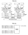
- FIG. 14 is a diagram explaining an example of the dispatch to an operational unit.
- FIG. 14 it will be explained about the case where four instructions are simultaneously decoded at a maximum.
- EXA_ONLY in FIG. 14 indicates an instruction that can be executed by only the EXA.
- the decoded instructions are assigned to RSEA or RSEB and the instructions are registered in "0 to 3" that are queues of RSEA or RSEB.
- instructions that can be executed by only the EXA are registered in RSEA.
- a priority circuit selects an oldest-ready instruction from each of RSEA and RSEB.
- "+INH_EXA(B)_P_TGR” that is a dispatch inhibition flag for each of the arithmetic units EXA and EXB is not on, the selected instruction is dispatched because "EXA(B)_VALID" of a priority selection signal of the arithmetic unit or that is a priority selection signal of the arithmetic unit becomes valid.
- the priority circuit after bubble up transmits and receives information such as various types of flags or conditions and resources such as real data and addresses required for operations are transmitted and received by a tag part illustrated at the right side of the priority circuit.
- the dispatch inhibition flag is not on (when the dispatch inhibition flag is "-INH_EXA(B)_P_TGR")
- the arithmetic unit EXA or EXB performs arithmetic processing of real data.
- FIG. 15 is a diagram explaining the functional block of the priority circuit of RSEA.
- the priority circuit sets only one bit of a signal "+P_EXA_SEL[0:9]” for selecting an entry to be dispatched to EXA to "1” by using a READY condition of each of nine instructions “+P_RSEA_0" to "+P_RSEA_9” that function as entries as an input condition.
- a READY condition of each entry includes, for example, "Condition 1: the entry is valid and is not dispatched”, "Condition 2: a source 1 register does not dependency relation or can be bypassed”, and "Condition 3: a source 2 register does not dependency relation or can be bypassed”.
- FIG. 16 is a diagram explaining the flow performed by the priority circuit of RSEA.
- the priority circuit decides the READY conditions of "P_RSEA_0" to "P_RSEA_9” from READY conditions (Step S1). Then, the priority circuit determines whether Condition 1 to Condition 3 are satisfied as the READY condition of "P_RSEA_9" (Step S2).
- the priority circuit in relation to the input of three conditions determines a queue from an old queue, i.e., the queue "9" among "0 to 9" when Condition 1 to Condition 3 are satisfied as illustrated in FIG. 17.
- FIG. 17 is a diagram illustrating the details of the priority circuit of RSEA.
- the priority circuit of RSEA selects "9” if it is “+P_RSEA_9_READY", for example.
- the priority circuit selects "8” if it is "+P_RSEA_8_READY”.
- FIG. 18 is a diagram illustrating the details of the priority circuit of RSEA. Furthermore, dispatch is performed on RSEB by a priority circuit similarly to RSEA.
- FIG. 19 is a diagram explaining an RSE sharing example.
- Patent Document 2 discloses a multi-threaded in-order superscalar processor having a fetch stage within which thread interleaving circuitry interleaves instructions taken from different program threads to form an interleaved stream of instructions which is then decoded and subject to issue. Hint generation circuitry within the fetch stage adds hint data to the threads indicating that parallel issue of an associated instruction is permitted with one or more other instructions.
- Patent Document 1 Japanese Laid-open Patent Publication No. 2000-105699
- Patent Document 2 US2008/0270749A1
- a processor comprising: an instruction decoder configured to decode an instruction and output the decoded instruction together with a flag which, when set, indicates that an instruction can be executed only by a specific arithmetic unit; a reservation station configured to receive and hold from the instruction decoder the decoded instruction and the flag and output the decoded instruction and the flag; a plurality of arithmetic units that each have an instruction queue configured to store a decoded instruction received from the reservation station and are each configured to execute a different operation based on the decoded instruction stored in the instruction queue; and a priority circuit configured to dispatch the decoded instruction from the reservation station to the specific arithmetic unit when the flag for the decoded instruction is set, and to dispatch the decoded instruction to the specific arithmetic unit or an arithmetic unit that is different from the specific arithmetic unit, and of which the instruction queue is vacant, when the flag for the decoded instruction is not set.
- a processing method of a processor that includes an instruction decoder, a reservation station, a plurality of arithmetic units that each have an instruction queue and each execute a different operation based on a decoded instruction stored in the instruction queue, and a priority circuit, the method comprising: decoding, using the instruction decoder, an instruction and outputting the decoded instruction together with a flag which, when set, indicates that an instruction can be executed only by a specific arithmetic unit; receiving and holding, using the reservation station, the decoded instruction and the flag output from the instruction decoder and outputting the decoded instruction and the flag; and dispatching, using the priority circuit, the decoded instruction output from the reservation station to the specific arithmetic unit when the flag output from the reservation station for the decoded instruction is set, and dispatching the decoded instruction output from the reservation station to the specific arithmetic unit or an arithmetic unit that is different from the specific arithmetic
- FIG. 1 is a diagram explaining an example of registration and dispatch to RSE according to the first embodiment.
- FIG. 1 will be explained about the case where four instructions can be simultaneously decoded at a maximum in order.
- an instruction decoder 100 registers a flag "EXA_ONLY" indicating an instruction that can be executed by only EXA as an entry tag of RSE. Then, a shared RSE 110 performs bubble up and inputs the registered flag "EXA_ONLY" information into a priority circuit 120. Moreover, the RSE 110 inputs corresponding real data "0 to 9" according to operations that are executed by an EXA 130 and an EXB 140 into the EXA 130 and the EXB 140.
- the priority circuit 120 determines the flag "EXA_ONLY" information and does not dispatch an entry of which the flag "EXA_ONLY" is on to the EXB 140 according to priority logic of dispatch.
- FIG. 2A is a diagram explaining an example of the dispatch to an arithmetic unit when the queue of RSEB is empty.
- Instruction 2 cannot be dispatched to EXB even if the EXB is vacant when RSE is divided into two like the conventional art. Therefore, in the present embodiment for sharing RSE, Instruction 2 is dispatched to the EXB when the flag EXA_ONLY is not on about Instruction 2.
- FIG. 2B is a diagram explaining an example of the dispatch to the arithmetic unit when a dispatch inhibition flag is on.
- FIG. 2C is a diagram explaining an example of the dispatch to the arithmetic unit when there is a dependency relation between Instruction 1 and Instruction 2.
- Instructions 1, 3, and 4 are assigned to the queues 9 to 7 of RSEA, and Instruction 2 is assigned to the queue 9 of RSEB, Instruction 3 cannot be issued from RSEB when RSE is divided into two like the conventional art. Therefore, in the present embodiment for sharing RSE, Instruction 2 is dispatched to the EXA and Instruction 3 and Instruction 4 are dispatched to the EXB when the flag EXA_ONLY is not on about Instruction 3 and instruction 4.
- FIG. 2D is a diagram explaining an example of the dispatch to the arithmetic unit when there is a dependency relation between Instruction 1, Instruction 2, and Instruction 3.
- Instruction 1 is assigned to the queue 9 of RSEA, and Instruction 2 and Instruction 3 are assigned to the queues 9 and 8 of RSEB, Instruction 2 is dispatched in the next cycle of Instruction 1 and Instruction 3 is dispatched in the next cycle of Instruction 2 when RSE is divided into two like the conventional art. Therefore, in the present embodiment for sharing RSE, when the flag EXA_ONLY is not on about Instruction 2 and Instruction 3, Instruction 2 is dispatched to EXA and Instruction 3 is dispatched to EXB at the same time in the next cycle of the cycle in which Instruction 1 is dispatched.
- FIG. 2E is a diagram explaining an example of the dispatch to the arithmetic unit when Instruction 1 and Instruction 2 are EXA_ONLY.
- Instructions 1 to 3 are respectively assigned to the queues 9 to 7 of RSEA, and the queue of RSEB is empty, Instruction 1 and Instruction 2 that are EXA_ONLY are clogged up and thus the following Instruction 3 that is not EXA_ONLY is not dispatched to the EXB when RSE is divided into two like the conventional art. Therefore, in the present embodiment for sharing RSE, Instruction 3 is dispatched to the EXB when the flag EXA_ONLY is not on about Instruction 3.
- the priority circuit dispatches an instruction to an arithmetic unit by sharing RSE on the basis of the dependency relation of instructions to be dispatched to the arithmetic unit, the flag EXA_ONLY, or the dispatch inhibition flag.
- the priority circuit dispatches an instruction to an arithmetic unit on the basis of the dependency relation of instructions or various types of flags, the efficiency of arithmetic processing can be promoted without errors in arithmetic processing.
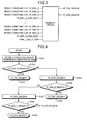
- FIG. 3 is a diagram explaining the functional block of the priority circuit of RSE according to the first embodiment.
- the priority circuit inputs READY conditions of nine instructions “+P_RSE_0" to "+P_RSE_9” that function as an entry, flags “+P_RSE_0_EXA_ONLY” to "+P_RSE_9_EXA_ONLY” depicting whether an instruction is EXA_ONLY, and a dispatch inhibition flag "+INH_EXA_P_TGR", and sets one bit of a signal "+P-EXA_SEL[0:9]” or "+P-EXB_SEL[0:9]" for selecting an entry to be dispatched to EXA or EXB to "1".
- the priority circuit depicted in FIG. 3 adds, to a priority condition according to the conventional art, a flag depicting that an instruction can be executed by only the EXA and a dispatch inhibition flag depicting that an instruction cannot be dispatched to EXA because an instruction that uses the EXA is being executed over multiple cycles.
- an output by the priority circuit is a signal for selecting an entry to be dispatched to the EXA or the EXB. In this case, because the READY condition of each entry is similar to the conventional art, their descriptions are omitted.
- FIG. 4 is a diagram explaining a flow of EXA_SEL performed by the priority circuit.
- the priority circuit decides the READY condition of "P_EXA_0" to "P_EXA_9” from the READY condition of RSE (Step S101). Then, the priority circuit determines whether Condition 1 to Condition 3 are satisfied as the READY condition of "P_EXA_9" (Step S102).
- FIG. 5 is a diagram explaining a flow of EXB_SEL[9] performed by the priority circuit.
- the priority circuit decides the READY condition of "P_EXA_9" from the READY condition of the RSE (Step S201). Then, the priority circuit determines whether Condition 1 to Condition 3 are satisfied as the READY condition of "P_EXA_9" (Step S202).
- FIG. 6 is a diagram explaining a flow of EXB_SEL[8] performed by the priority circuit.
- the priority circuit decides the READY conditions of "P_EXA_9" and "P_EXA_8" from the READY condition of RSE (Step S301). Then, the priority circuit determines whether Condition 1 to Condition 3 are satisfied as the READY condition of "P_EXA_8" (Step S302).
- Step S304 the priority circuit determines whether Condition 1 to Condition 3 are satisfied as the READY condition of "P_EXA_9" (Step S305).
- entries after "+P_EXB_SEL[8]" are selected in accordance with the READY conditions of all the preceding entries. It should be noted that the flows to EXA and EXB in FIGS. 4 to 6 are simultaneously executed.
- the priority circuit related to the input of three conditions does not dispatch an instruction that can be executed by only EXA to EXB by including, for example, "-P_RSE_0(0 to 9)_EXA_ONLY" in a logic for deciding the READY status of an entry of each EXA.
- FIG. 7 is a diagram illustrating the details of the priority circuit of RSE.
- FIG. 8 is a diagram illustrating an example of an EXA selection logic unit of the priority circuit of RSE.
- the EXA selection logic unit of the priority circuit of RSE in the flow selects "9” if it is “+P_EXA_9_READY” and selects "8” if it is “+P_EXA_8_READY” in a state where "9” is not selected "-P_EXA_9_READY".
- the EXA selection logic unit selects "7” in the case of "-P_EXA_9_READY", “-P_EXA_8_READY", and "+P_EXA_7_READY". In this way, the EXA selection logic unit selects "0” if it is "+P_EXA_0_READY” in the case of "-P_EXA_9_READY” to "-P_EXA_1_READY".
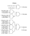
- FIG. 9 is a diagram illustrating an example of an EXB selection logic unit of the priority circuit of RSE.
- the EXB selection logic unit of the priority circuit of RSE in the flow dispatches a second oldest ready entry to the EXB on the basis of the READY signals of EXA and EXB.
- the dispatch inhibition flag "+INH_EXA_P_TGR" is "1"
- the EXB selection logic unit dispatches an oldest ready entry to the EXB.
- "EXA_VALID" becomes "0” due to "-INH_EXA_P_TGR" though an oldest ready entry is dispatched to the EXA, it leads to inhibit an operation in the EXA and thus the operation is not executed.
- the instruction decoder inputs EXA_ONLY indicating that an instruction can be executed by only an arithmetic unit A into one reservation station and the priority circuit dispatches an instruction to an arithmetic unit B if the queue of the arithmetic unit B is vacant when it is determined that the EXA_ONLY is on in accordance with the input of the EXA_ONLY performed by the reservation station. Therefore, it is possible to improve the efficiency of arithmetic processing performed by an arithmetic unit without errors.
- the priority circuit dispatches an instruction to the arithmetic unit B if the dispatch inhibition flag is on and the queue of the arithmetic unit B is vacant. Therefore, it is possible to promote the efficiency of arithmetic processing performed by an arithmetic unit.
- the present invention can be realized by an arithmetic processing unit (processor) that includes the priority circuit.
- the priority circuit may be applied to the processor illustrated in FIG. 10 .
- the arithmetic unit may be applied to a floating point arithmetic unit.
- processing procedures, control procedures, concrete titles, and information including various types of data and parameters for example, the concrete title of "dispatch inhibition flag” and the like), which are described in the document and the drawings, can be arbitrarily changed except that they are specially mentioned.
- each component of each circuit illustrated in the drawings is a functional concept. Therefore, these components are not necessarily constituted physically as illustrated in the drawings. In other words, the specific configuration of dispersion/integration of each circuit is not limited to the illustrated configuration. Therefore, all or a part of each circuit can dispersed or integrated functionally or physically in an optional unit in accordance with various types of loads or operating conditions.
- the invention also provides a computer program or a computer program product for carrying out any of the methods described herein, and a computer readable medium having stored thereon a program for carrying out any of the methods described herein.
- a computer program embodying the invention may be stored on a computer-readable medium, or it could, for example, be in the form of a signal such as a downloadable data signal provided from an Internet website, or it could be in any other form.
Landscapes
- Engineering & Computer Science (AREA)
- Software Systems (AREA)
- Theoretical Computer Science (AREA)
- Physics & Mathematics (AREA)
- General Physics & Mathematics (AREA)
- General Engineering & Computer Science (AREA)
- Computational Mathematics (AREA)
- Mathematical Analysis (AREA)
- Mathematical Optimization (AREA)
- Pure & Applied Mathematics (AREA)
- Advance Control (AREA)
Claims (4)
- Prozessor, welcher Folgendes umfasst:einen Befehlsdecoder (100), der zum Decodieren eines Befehls und Ausgeben des decodierten Befehls zusammen mit einem Flag (EXA ONLY), welches, wenn es gesetzt ist, anzeigt, dass ein Befehl nur durch ein spezifisches Rechenwerk (130) ausgeführt werden kann, konfiguriert ist;eine Reservierungsstation (110), welche zum Empfangen und Halten des decodierten Befehls und des Flags von dem Befehlsdecoder (100) und Ausgeben des decodierten Befehls und des Flags konfiguriert ist;mehrere Rechenwerke (130, 140), die jeweils eine Befehlswarteschlange aufweisen, die zum Speichern eines decodierten Befehls, der von der Reservierungsstation empfangen wurde, konfiguriert ist, und die jeweils zum Ausführen einer unterschiedlichen Operation basierend auf dem decodierten Befehl, der in der Befehlswarteschlange gespeichert ist, konfiguriert sind; undeine Prioritätsschaltung (120), die zum Versenden des decodierten Befehls von der Reservierungsstation an das spezifische Rechenwerk (130), wenn das Flag für den decodierten Befehl gesetzt ist, und zum Versenden des decodierten Befehls an das spezifische Rechenwerk (130) oder ein Rechenwerk (140), das sich von dem spezifischen Rechenwerk (130) unterscheidet und dessen Befehlswarteschlange leer ist, wenn das Flag für den decodierten Befehl nicht gesetzt ist, konfiguriert ist.
- Prozessor nach Anspruch 1, wobei die Prioritätsschaltung (120) zum Empfangen eines Versandverhinderungs-Flags, welches, wenn es gesetzt ist, anzeigt, dass der decodierte Befehl nicht an das spezifische Rechenwerk (130) versandt werden kann, und zum Versenden des decodierten Befehls an ein Rechenwerk (140), das sich von dem spezifischen Rechenwerk (130) unterscheidet und dessen Befehlswarteschlange leer ist, wenn das empfangene Versandverhinderungs-Flag für das spezifische Rechenwerk (130) gesetzt ist, konfiguriert ist.
- Verarbeitungsverfahren eines Prozessors, welcher einen Befehlsdecoder (100), eine Reservierungsstation (110), mehrere Rechenwerke (130, 140), die jeweils eine Befehlswarteschlange aufweisen und jeweils eine unterschiedliche Operation basierend auf einem decodierten Befehl, der in der Befehlswarteschlange gespeichert ist, ausführen, und eine Prioritätsschaltung (120) beinhaltet, wobei das Verfahren Folgendes umfasst:Decodieren, unter Verwendung des Befehlsdecoders (100), eines Befehls und Ausgeben des decodierten Befehls zusammen mit einem Flag, welches, wenn es gesetzt ist, anzeigt, dass ein Befehl nur durch ein spezifisches Rechenwerk (130) ausgeführt werden kann;Empfangen und Halten, unter Verwendung der Reservierungsstation (110), des decodierten Befehls und des Flags, die vom Befehlsdecoder (100) ausgegeben wurden, und Ausgeben des decodierten Befehls und des Flags; undVersenden, unter Verwendung der Prioritätsschaltung (120), des decodierten Befehls, der von der Reservierungsstation (110) ausgegeben wurde, an das spezifische Rechenwerk (130), wenn das Flag, das von der Reservierungsstation (110) für den decodierten Befehl ausgegeben wurde, gesetzt ist, und Versenden des decodierten Befehls, der von der Reservierungsstation (110) ausgegeben wurde, an das spezifische Rechenwerk (130) oder ein Rechenwerk (140), das sich von dem spezifischen Rechenwerk (130) unterscheidet und dessen Befehlswarteschlange leer ist, wenn das Flag, das von der Reservierungsstation (110) für den decodierten Befehl ausgegeben wurde, nicht gesetzt ist.
- Verarbeitungsverfahren nach Anspruch 3, wobei das Versenden das Empfangen eines Versandverhinderungs-Flags, welches, wenn es gesetzt ist, anzeigt, dass der decodierte Befehl nicht an das spezifische Rechenwerk (130) versandt werden kann, und das Versenden des decodierten Befehls an ein Rechenwerk (140), das sich von dem spezifischen Rechenwerk (130) unterscheidet und dessen Befehlswarteschlange leer ist, wenn das empfangene Versandverhinderungs-Flag für das spezifische Rechenwerk (130) gesetzt ist, beinhaltet.
Applications Claiming Priority (1)
| Application Number | Priority Date | Filing Date | Title |
|---|---|---|---|
| JP2009154374A JP2011008732A (ja) | 2009-06-29 | 2009-06-29 | プライオリティ回路、演算処理装置及び演算処理方法 |
Publications (2)
| Publication Number | Publication Date |
|---|---|
| EP2270652A1 EP2270652A1 (de) | 2011-01-05 |
| EP2270652B1 true EP2270652B1 (de) | 2013-03-27 |
Family
ID=42668277
Family Applications (1)
| Application Number | Title | Priority Date | Filing Date |
|---|---|---|---|
| EP10167671A Not-in-force EP2270652B1 (de) | 2009-06-29 | 2010-06-29 | Prioritätsschaltkreis zum Zuteilen von Befehlen in einem superskalaren Prozessor, welcher eine gemeinsam benutzte Reservation Station aufweist, sowie eine Verarbeitungsmethode |
Country Status (3)
| Country | Link |
|---|---|
| US (1) | US8516223B2 (de) |
| EP (1) | EP2270652B1 (de) |
| JP (1) | JP2011008732A (de) |
Families Citing this family (6)
| Publication number | Priority date | Publication date | Assignee | Title |
|---|---|---|---|---|
| JP2013206095A (ja) * | 2012-03-28 | 2013-10-07 | Fujitsu Ltd | データ処理装置及びデータ処理装置の制御方法 |
| JP2014002555A (ja) * | 2012-06-18 | 2014-01-09 | Fujitsu Ltd | プロセッサ |
| US9317294B2 (en) | 2012-12-06 | 2016-04-19 | International Business Machines Corporation | Concurrent multiple instruction issue of non-pipelined instructions using non-pipelined operation resources in another processing core |
| CN104657114B (zh) * | 2015-03-03 | 2019-09-06 | 上海兆芯集成电路有限公司 | 并行化的多分派系统和用于排序队列仲裁的方法 |
| JP6520416B2 (ja) | 2015-06-02 | 2019-05-29 | 富士通株式会社 | 演算処理装置および演算処理装置の処理方法 |
| US12039329B2 (en) * | 2020-12-24 | 2024-07-16 | Intel Corporation | Methods, systems, and apparatuses to optimize partial flag updating instructions via dynamic two-pass execution in a processor |
Family Cites Families (11)
| Publication number | Priority date | Publication date | Assignee | Title |
|---|---|---|---|---|
| GB2263565B (en) * | 1992-01-23 | 1995-08-30 | Intel Corp | Microprocessor with apparatus for parallel execution of instructions |
| US5592679A (en) * | 1994-11-14 | 1997-01-07 | Sun Microsystems, Inc. | Apparatus and method for distributed control in a processor architecture |
| US5809323A (en) * | 1995-09-19 | 1998-09-15 | International Business Machines Corporation | Method and apparatus for executing fixed-point instructions within idle execution units of a superscalar processor |
| US6105128A (en) * | 1998-04-30 | 2000-08-15 | Intel Corporation | Method and apparatus for dispatching instructions to execution units in waves |
| US6249855B1 (en) * | 1998-06-02 | 2001-06-19 | Compaq Computer Corporation | Arbiter system for central processing unit having dual dominoed encoders for four instruction issue per machine cycle |
| US6742111B2 (en) | 1998-08-31 | 2004-05-25 | Stmicroelectronics, Inc. | Reservation stations to increase instruction level parallelism |
| JP3560482B2 (ja) * | 1998-12-17 | 2004-09-02 | 富士通株式会社 | 命令制御装置 |
| JP4025493B2 (ja) * | 2000-08-08 | 2007-12-19 | 富士通株式会社 | 適切な発行先に命令を発行する命令発行装置 |
| JP3577052B2 (ja) * | 2002-03-19 | 2004-10-13 | 株式会社東芝 | 命令発行装置及び命令発行方法 |
| JP4952580B2 (ja) * | 2005-04-21 | 2012-06-13 | 富士通株式会社 | プロセッサ装置 |
| US7707390B2 (en) * | 2007-04-25 | 2010-04-27 | Arm Limited | Instruction issue control within a multi-threaded in-order superscalar processor |
-
2009
- 2009-06-29 JP JP2009154374A patent/JP2011008732A/ja active Pending
-
2010
- 2010-06-29 US US12/801,868 patent/US8516223B2/en not_active Expired - Fee Related
- 2010-06-29 EP EP10167671A patent/EP2270652B1/de not_active Not-in-force
Also Published As
| Publication number | Publication date |
|---|---|
| US8516223B2 (en) | 2013-08-20 |
| JP2011008732A (ja) | 2011-01-13 |
| US20100332802A1 (en) | 2010-12-30 |
| EP2270652A1 (de) | 2011-01-05 |
Similar Documents
| Publication | Publication Date | Title |
|---|---|---|
| US5699537A (en) | Processor microarchitecture for efficient dynamic scheduling and execution of chains of dependent instructions | |
| EP1152329B1 (de) | Verfahren, Computerprogrammprodukt und Vorrichtung zum Identifizieren von teilbaren Paketen in einem Multi-threaded VLIW Prozessor | |
| CA2337172C (en) | Method and apparatus for allocating functional units in a multithreaded vliw processor | |
| US6334182B2 (en) | Scheduling operations using a dependency matrix | |
| KR100464406B1 (ko) | 가변길이 vliw 명령어를 위한 디스패치 장치 및 방법 | |
| TWI497412B (zh) | 用於使用相依矩陣追蹤解除配置之載入指令之方法、處理器及裝置 | |
| CN101720460B (zh) | 紧凑指令组编码 | |
| CN101763251B (zh) | 含有译码缓冲装置的多线程的微处理器 | |
| CN112540789B (zh) | 一种指令处理装置、处理器及其处理方法 | |
| EP2270652B1 (de) | Prioritätsschaltkreis zum Zuteilen von Befehlen in einem superskalaren Prozessor, welcher eine gemeinsam benutzte Reservation Station aufweist, sowie eine Verarbeitungsmethode | |
| WO2017053045A1 (en) | CONFIGURING COARSE-GRAINED RECONFIGURABLE ARRAYS (CGRAs) FOR DATAFLOW INSTRUCTION BLOCK EXECUTION IN BLOCK-BASED DATAFLOW INSTRUCTION SET ARCHITECTURES (ISAs) | |
| CN112540796B (zh) | 一种指令处理装置、处理器及其处理方法 | |
| US7096343B1 (en) | Method and apparatus for splitting packets in multithreaded VLIW processor | |
| JP2008242647A (ja) | プロセッサ | |
| CN112379928B (zh) | 指令调度方法以及包括指令调度单元的处理器 | |
| JP4996945B2 (ja) | データ処理装置、データ処理方法 | |
| JP5093237B2 (ja) | 命令処理装置 | |
| US20150046689A1 (en) | Arithmetic processing unit and method for controlling arithmetic processing unit | |
| JP7004905B2 (ja) | 演算処理装置及び演算処理装置の制御方法 | |
| JP6307975B2 (ja) | 演算処理装置及び演算処理装置の制御方法 | |
| JP2025154190A (ja) | マトリクススケジューラを備えるプロセッサ及び情報処理装置 | |
| JP2011128672A (ja) | スーパースカラプロセッサ及びその命令処理方法 | |
| JP2012008622A (ja) | 演算ユニット |
Legal Events
| Date | Code | Title | Description |
|---|---|---|---|
| PUAI | Public reference made under article 153(3) epc to a published international application that has entered the european phase |
Free format text: ORIGINAL CODE: 0009012 |
|
| AK | Designated contracting states |
Kind code of ref document: A1 Designated state(s): AL AT BE BG CH CY CZ DE DK EE ES FI FR GB GR HR HU IE IS IT LI LT LU LV MC MK MT NL NO PL PT RO SE SI SK SM TR |
|
| AX | Request for extension of the european patent |
Extension state: BA ME RS |
|
| 17P | Request for examination filed |
Effective date: 20110629 |
|
| 17Q | First examination report despatched |
Effective date: 20110818 |
|
| GRAP | Despatch of communication of intention to grant a patent |
Free format text: ORIGINAL CODE: EPIDOSNIGR1 |
|
| GRAS | Grant fee paid |
Free format text: ORIGINAL CODE: EPIDOSNIGR3 |
|
| GRAA | (expected) grant |
Free format text: ORIGINAL CODE: 0009210 |
|
| AK | Designated contracting states |
Kind code of ref document: B1 Designated state(s): AL AT BE BG CH CY CZ DE DK EE ES FI FR GB GR HR HU IE IS IT LI LT LU LV MC MK MT NL NO PL PT RO SE SI SK SM TR |
|
| REG | Reference to a national code |
Ref country code: GB Ref legal event code: FG4D |
|
| REG | Reference to a national code |
Ref country code: CH Ref legal event code: EP |
|
| REG | Reference to a national code |
Ref country code: AT Ref legal event code: REF Ref document number: 603777 Country of ref document: AT Kind code of ref document: T Effective date: 20130415 |
|
| REG | Reference to a national code |
Ref country code: IE Ref legal event code: FG4D |
|
| REG | Reference to a national code |
Ref country code: DE Ref legal event code: R096 Ref document number: 602010005740 Country of ref document: DE Effective date: 20130523 |
|
| PG25 | Lapsed in a contracting state [announced via postgrant information from national office to epo] |
Ref country code: SE Free format text: LAPSE BECAUSE OF FAILURE TO SUBMIT A TRANSLATION OF THE DESCRIPTION OR TO PAY THE FEE WITHIN THE PRESCRIBED TIME-LIMIT Effective date: 20130327 Ref country code: NO Free format text: LAPSE BECAUSE OF FAILURE TO SUBMIT A TRANSLATION OF THE DESCRIPTION OR TO PAY THE FEE WITHIN THE PRESCRIBED TIME-LIMIT Effective date: 20130627 Ref country code: BG Free format text: LAPSE BECAUSE OF FAILURE TO SUBMIT A TRANSLATION OF THE DESCRIPTION OR TO PAY THE FEE WITHIN THE PRESCRIBED TIME-LIMIT Effective date: 20130627 Ref country code: LT Free format text: LAPSE BECAUSE OF FAILURE TO SUBMIT A TRANSLATION OF THE DESCRIPTION OR TO PAY THE FEE WITHIN THE PRESCRIBED TIME-LIMIT Effective date: 20130327 |
|
| REG | Reference to a national code |
Ref country code: AT Ref legal event code: MK05 Ref document number: 603777 Country of ref document: AT Kind code of ref document: T Effective date: 20130327 |
|
| REG | Reference to a national code |
Ref country code: LT Ref legal event code: MG4D |
|
| PG25 | Lapsed in a contracting state [announced via postgrant information from national office to epo] |
Ref country code: FI Free format text: LAPSE BECAUSE OF FAILURE TO SUBMIT A TRANSLATION OF THE DESCRIPTION OR TO PAY THE FEE WITHIN THE PRESCRIBED TIME-LIMIT Effective date: 20130327 Ref country code: LV Free format text: LAPSE BECAUSE OF FAILURE TO SUBMIT A TRANSLATION OF THE DESCRIPTION OR TO PAY THE FEE WITHIN THE PRESCRIBED TIME-LIMIT Effective date: 20130327 Ref country code: SI Free format text: LAPSE BECAUSE OF FAILURE TO SUBMIT A TRANSLATION OF THE DESCRIPTION OR TO PAY THE FEE WITHIN THE PRESCRIBED TIME-LIMIT Effective date: 20130327 Ref country code: GR Free format text: LAPSE BECAUSE OF FAILURE TO SUBMIT A TRANSLATION OF THE DESCRIPTION OR TO PAY THE FEE WITHIN THE PRESCRIBED TIME-LIMIT Effective date: 20130628 |
|
| REG | Reference to a national code |
Ref country code: NL Ref legal event code: VDEP Effective date: 20130327 |
|
| PG25 | Lapsed in a contracting state [announced via postgrant information from national office to epo] |
Ref country code: BE Free format text: LAPSE BECAUSE OF FAILURE TO SUBMIT A TRANSLATION OF THE DESCRIPTION OR TO PAY THE FEE WITHIN THE PRESCRIBED TIME-LIMIT Effective date: 20130327 Ref country code: HR Free format text: LAPSE BECAUSE OF FAILURE TO SUBMIT A TRANSLATION OF THE DESCRIPTION OR TO PAY THE FEE WITHIN THE PRESCRIBED TIME-LIMIT Effective date: 20130327 |
|
| PG25 | Lapsed in a contracting state [announced via postgrant information from national office to epo] |
Ref country code: CZ Free format text: LAPSE BECAUSE OF FAILURE TO SUBMIT A TRANSLATION OF THE DESCRIPTION OR TO PAY THE FEE WITHIN THE PRESCRIBED TIME-LIMIT Effective date: 20130327 Ref country code: RO Free format text: LAPSE BECAUSE OF FAILURE TO SUBMIT A TRANSLATION OF THE DESCRIPTION OR TO PAY THE FEE WITHIN THE PRESCRIBED TIME-LIMIT Effective date: 20130327 Ref country code: IS Free format text: LAPSE BECAUSE OF FAILURE TO SUBMIT A TRANSLATION OF THE DESCRIPTION OR TO PAY THE FEE WITHIN THE PRESCRIBED TIME-LIMIT Effective date: 20130727 Ref country code: SK Free format text: LAPSE BECAUSE OF FAILURE TO SUBMIT A TRANSLATION OF THE DESCRIPTION OR TO PAY THE FEE WITHIN THE PRESCRIBED TIME-LIMIT Effective date: 20130327 Ref country code: PT Free format text: LAPSE BECAUSE OF FAILURE TO SUBMIT A TRANSLATION OF THE DESCRIPTION OR TO PAY THE FEE WITHIN THE PRESCRIBED TIME-LIMIT Effective date: 20130729 Ref country code: ES Free format text: LAPSE BECAUSE OF FAILURE TO SUBMIT A TRANSLATION OF THE DESCRIPTION OR TO PAY THE FEE WITHIN THE PRESCRIBED TIME-LIMIT Effective date: 20130708 Ref country code: EE Free format text: LAPSE BECAUSE OF FAILURE TO SUBMIT A TRANSLATION OF THE DESCRIPTION OR TO PAY THE FEE WITHIN THE PRESCRIBED TIME-LIMIT Effective date: 20130327 Ref country code: NL Free format text: LAPSE BECAUSE OF FAILURE TO SUBMIT A TRANSLATION OF THE DESCRIPTION OR TO PAY THE FEE WITHIN THE PRESCRIBED TIME-LIMIT Effective date: 20130327 Ref country code: AT Free format text: LAPSE BECAUSE OF FAILURE TO SUBMIT A TRANSLATION OF THE DESCRIPTION OR TO PAY THE FEE WITHIN THE PRESCRIBED TIME-LIMIT Effective date: 20130327 |
|
| PG25 | Lapsed in a contracting state [announced via postgrant information from national office to epo] |
Ref country code: CY Free format text: LAPSE BECAUSE OF FAILURE TO SUBMIT A TRANSLATION OF THE DESCRIPTION OR TO PAY THE FEE WITHIN THE PRESCRIBED TIME-LIMIT Effective date: 20130327 Ref country code: PL Free format text: LAPSE BECAUSE OF FAILURE TO SUBMIT A TRANSLATION OF THE DESCRIPTION OR TO PAY THE FEE WITHIN THE PRESCRIBED TIME-LIMIT Effective date: 20130327 |
|
| PG25 | Lapsed in a contracting state [announced via postgrant information from national office to epo] |
Ref country code: MC Free format text: LAPSE BECAUSE OF FAILURE TO SUBMIT A TRANSLATION OF THE DESCRIPTION OR TO PAY THE FEE WITHIN THE PRESCRIBED TIME-LIMIT Effective date: 20130327 Ref country code: DK Free format text: LAPSE BECAUSE OF FAILURE TO SUBMIT A TRANSLATION OF THE DESCRIPTION OR TO PAY THE FEE WITHIN THE PRESCRIBED TIME-LIMIT Effective date: 20130327 |
|
| PLBE | No opposition filed within time limit |
Free format text: ORIGINAL CODE: 0009261 |
|
| STAA | Information on the status of an ep patent application or granted ep patent |
Free format text: STATUS: NO OPPOSITION FILED WITHIN TIME LIMIT |
|
| PG25 | Lapsed in a contracting state [announced via postgrant information from national office to epo] |
Ref country code: IT Free format text: LAPSE BECAUSE OF FAILURE TO SUBMIT A TRANSLATION OF THE DESCRIPTION OR TO PAY THE FEE WITHIN THE PRESCRIBED TIME-LIMIT Effective date: 20130327 |
|
| 26N | No opposition filed |
Effective date: 20140103 |
|
| REG | Reference to a national code |
Ref country code: IE Ref legal event code: MM4A |
|
| REG | Reference to a national code |
Ref country code: DE Ref legal event code: R097 Ref document number: 602010005740 Country of ref document: DE Effective date: 20140103 |
|
| PG25 | Lapsed in a contracting state [announced via postgrant information from national office to epo] |
Ref country code: IE Free format text: LAPSE BECAUSE OF NON-PAYMENT OF DUE FEES Effective date: 20130629 |
|
| PGFP | Annual fee paid to national office [announced via postgrant information from national office to epo] |
Ref country code: GB Payment date: 20140404 Year of fee payment: 5 |
|
| PGFP | Annual fee paid to national office [announced via postgrant information from national office to epo] |
Ref country code: DE Payment date: 20140625 Year of fee payment: 5 |
|
| PGFP | Annual fee paid to national office [announced via postgrant information from national office to epo] |
Ref country code: FR Payment date: 20140609 Year of fee payment: 5 |
|
| REG | Reference to a national code |
Ref country code: CH Ref legal event code: PL |
|
| PG25 | Lapsed in a contracting state [announced via postgrant information from national office to epo] |
Ref country code: MT Free format text: LAPSE BECAUSE OF FAILURE TO SUBMIT A TRANSLATION OF THE DESCRIPTION OR TO PAY THE FEE WITHIN THE PRESCRIBED TIME-LIMIT Effective date: 20130327 |
|
| PG25 | Lapsed in a contracting state [announced via postgrant information from national office to epo] |
Ref country code: CH Free format text: LAPSE BECAUSE OF NON-PAYMENT OF DUE FEES Effective date: 20140630 Ref country code: LI Free format text: LAPSE BECAUSE OF NON-PAYMENT OF DUE FEES Effective date: 20140630 |
|
| PG25 | Lapsed in a contracting state [announced via postgrant information from national office to epo] |
Ref country code: SM Free format text: LAPSE BECAUSE OF FAILURE TO SUBMIT A TRANSLATION OF THE DESCRIPTION OR TO PAY THE FEE WITHIN THE PRESCRIBED TIME-LIMIT Effective date: 20130327 |
|
| PG25 | Lapsed in a contracting state [announced via postgrant information from national office to epo] |
Ref country code: TR Free format text: LAPSE BECAUSE OF FAILURE TO SUBMIT A TRANSLATION OF THE DESCRIPTION OR TO PAY THE FEE WITHIN THE PRESCRIBED TIME-LIMIT Effective date: 20130327 |
|
| PG25 | Lapsed in a contracting state [announced via postgrant information from national office to epo] |
Ref country code: LU Free format text: LAPSE BECAUSE OF NON-PAYMENT OF DUE FEES Effective date: 20130629 Ref country code: MK Free format text: LAPSE BECAUSE OF FAILURE TO SUBMIT A TRANSLATION OF THE DESCRIPTION OR TO PAY THE FEE WITHIN THE PRESCRIBED TIME-LIMIT Effective date: 20130327 Ref country code: HU Free format text: LAPSE BECAUSE OF FAILURE TO SUBMIT A TRANSLATION OF THE DESCRIPTION OR TO PAY THE FEE WITHIN THE PRESCRIBED TIME-LIMIT; INVALID AB INITIO Effective date: 20100629 |
|
| REG | Reference to a national code |
Ref country code: DE Ref legal event code: R119 Ref document number: 602010005740 Country of ref document: DE |
|
| GBPC | Gb: european patent ceased through non-payment of renewal fee |
Effective date: 20150629 |
|
| REG | Reference to a national code |
Ref country code: FR Ref legal event code: ST Effective date: 20160229 |
|
| PG25 | Lapsed in a contracting state [announced via postgrant information from national office to epo] |
Ref country code: GB Free format text: LAPSE BECAUSE OF NON-PAYMENT OF DUE FEES Effective date: 20150629 Ref country code: DE Free format text: LAPSE BECAUSE OF NON-PAYMENT OF DUE FEES Effective date: 20160101 |
|
| PG25 | Lapsed in a contracting state [announced via postgrant information from national office to epo] |
Ref country code: FR Free format text: LAPSE BECAUSE OF NON-PAYMENT OF DUE FEES Effective date: 20150630 |
|
| PG25 | Lapsed in a contracting state [announced via postgrant information from national office to epo] |
Ref country code: AL Free format text: LAPSE BECAUSE OF FAILURE TO SUBMIT A TRANSLATION OF THE DESCRIPTION OR TO PAY THE FEE WITHIN THE PRESCRIBED TIME-LIMIT Effective date: 20130327 |