EP2267782A2 - Control of tunneling junction in a hetero tunnel field effect transistor - Google Patents
Control of tunneling junction in a hetero tunnel field effect transistor Download PDFInfo
- Publication number
- EP2267782A2 EP2267782A2 EP10166385A EP10166385A EP2267782A2 EP 2267782 A2 EP2267782 A2 EP 2267782A2 EP 10166385 A EP10166385 A EP 10166385A EP 10166385 A EP10166385 A EP 10166385A EP 2267782 A2 EP2267782 A2 EP 2267782A2
- Authority
- EP
- European Patent Office
- Prior art keywords
- source
- region
- channel
- semiconductor material
- tfet
- Prior art date
- Legal status (The legal status is an assumption and is not a legal conclusion. Google has not performed a legal analysis and makes no representation as to the accuracy of the status listed.)
- Withdrawn
Links
Images




Classifications
-
- H—ELECTRICITY
- H10—SEMICONDUCTOR DEVICES; ELECTRIC SOLID-STATE DEVICES NOT OTHERWISE PROVIDED FOR
- H10D—INORGANIC ELECTRIC SEMICONDUCTOR DEVICES
- H10D12/00—Bipolar devices controlled by the field effect, e.g. insulated-gate bipolar transistors [IGBT]
- H10D12/211—Gated diodes
-
- H—ELECTRICITY
- H10—SEMICONDUCTOR DEVICES; ELECTRIC SOLID-STATE DEVICES NOT OTHERWISE PROVIDED FOR
- H10D—INORGANIC ELECTRIC SEMICONDUCTOR DEVICES
- H10D62/00—Semiconductor bodies, or regions thereof, of devices having potential barriers
- H10D62/10—Shapes, relative sizes or dispositions of the regions of the semiconductor bodies; Shapes of the semiconductor bodies
- H10D62/117—Shapes of semiconductor bodies
- H10D62/118—Nanostructure semiconductor bodies
- H10D62/119—Nanowire, nanosheet or nanotube semiconductor bodies
- H10D62/122—Nanowire, nanosheet or nanotube semiconductor bodies oriented at angles to substrates, e.g. perpendicular to substrates
-
- H—ELECTRICITY
- H10—SEMICONDUCTOR DEVICES; ELECTRIC SOLID-STATE DEVICES NOT OTHERWISE PROVIDED FOR
- H10D—INORGANIC ELECTRIC SEMICONDUCTOR DEVICES
- H10D62/00—Semiconductor bodies, or regions thereof, of devices having potential barriers
- H10D62/80—Semiconductor bodies, or regions thereof, of devices having potential barriers characterised by the materials
- H10D62/82—Heterojunctions
- H10D62/822—Heterojunctions comprising only Group IV materials heterojunctions, e.g. Si/Ge heterojunctions
-
- H—ELECTRICITY
- H10—SEMICONDUCTOR DEVICES; ELECTRIC SOLID-STATE DEVICES NOT OTHERWISE PROVIDED FOR
- H10D—INORGANIC ELECTRIC SEMICONDUCTOR DEVICES
- H10D62/00—Semiconductor bodies, or regions thereof, of devices having potential barriers
- H10D62/80—Semiconductor bodies, or regions thereof, of devices having potential barriers characterised by the materials
- H10D62/83—Semiconductor bodies, or regions thereof, of devices having potential barriers characterised by the materials being Group IV materials, e.g. B-doped Si or undoped Ge
- H10D62/832—Semiconductor bodies, or regions thereof, of devices having potential barriers characterised by the materials being Group IV materials, e.g. B-doped Si or undoped Ge being Group IV materials comprising two or more elements, e.g. SiGe
Definitions
- the present invention relates to the field of semiconductor devices and nanotechnology.
- the invention relates to a nanostructure semiconductor device, more specifically to a tunnel field effect transistor having a segmented nanostructure (e.g. a heterostructure nanowire).
- a segmented nanostructure e.g. a heterostructure nanowire
- the invention relates to a method for manufacturing tunnel field effect transistor devices with integrated nanostructures such as nanowires having improved device properties.
- Microelectronic devices are generally fabricated on semiconductor substrates as integrated circuits.
- a complementary metal-oxide-semiconductor (CMOS) field effect transistor is one of the core elements of the integrated circuits.
- CMOS complementary metal-oxide-semiconductor
- Dimensions and operating voltages of CMOS transistors are continuously reduced, or scaled down, to obtain ever-higher performance and packaging density of the integrated circuits.
- CMOS transistors One of the problems due to the scaling down of CMOS transistors, is that the power consumption keeps increasing. This is partly because leakage currents are increasing (e.g. due to short channel effects) and because it becomes difficult to decrease the supply voltage. The latter is mainly due to the fact that the subthreshold slope is limited to minimally about 60 mV/decade, such that switching the transistor from ON to OFF needs a certain voltage variation and therefore a minimum supply voltage.
- Tunnel field-effect transistors are typically advertised as successors of metal-oxide semiconductor field-effect transistors (MOSFETs), because of their absence of short-channel effects and because of their resulting low off-currents.
- MOSFETs metal-oxide semiconductor field-effect transistors
- Another advantage of TFETs is that the subthreshold slope can be less than 60 mV/dec, the physical limit of conventional MOSFETs, such that potentially lower supply voltages can be used.
- TFETs typically suffer from low on-currents, a drawback related to the large resistance of the tunnel barrier.
- Verhulst et al [ A.S. Verhulst et al, J. Appl. Phys., 104(6):064514, 2008 ] have shown that the ON current of a tunnel field-effect transistor can be boosted by using a p-doped Ge (or p-doped SiGe) source in combination with a Si channel and n doped drain.
- the increase in ON current depends strongly on the abruptness of the (p) doping profile at the (Si)Ge/ intrinsic Si tunneling junction (see FIG. 1 ). This is a challenging task to achieve, as the p -type dopants (e.g. B dopants) readily diffuse into the Si channel due to the thermal budget during the device fabrication.
- TFET tunnel Field Effect transistor
- the problem to be solved is avoiding out-diffusion of the dopants from the doped source towards the channel region such that a steep dopant profile is achieved at the interface of the source and channel.
- the problem of out diffusion especially occurs in heterostructures where the dopant of the source has lower diffusion kinetics in the channel material than in the source material. Since the doped source is in direct contact with the intrinsic channel, a source made of Ge (or SiGe) having dopants such as B which have higher diffusivity in Si compared to Ge (or SiGe) will always diffuse towards the Si channel, especially due to the thermal budget during fabrication of the TFET.
- embodiments of the present invention disclose a method for providing a tunnel field effect transistor (TFET) comprising at least a source region and a channel region, with a heterojunction between the source and the channel region, thereby eliminating or at least reducing drastically the out-diffusion of the dopants of the source into the (intrinsic) channel region.
- the method comprises at least the steps of:
- a method according to embodiments the present invention has the advantage that the thickness of the transition layer can be engineered such that the transition layer coincides with a steep transition step from the doped source region to the lowly doped or undoped channel region, thereby maximizing the tunneling current.
- doping the source region and the drain region comprises selectively doping the as-deposited source and drain regions to a desired doping level with a desired dopant type, for example 10 18 /cc to 10 21 /cc, to form a highly doped source and drain region, for example the doping level of the source region and/or the drain region may be in the range of 10 19 /cc to 5x10 20 /cc.
- the dopant elements used for doping may be p-type dopants or alternatively n-type dopants.
- source and drain semiconductor material may be in situ doped during deposition.
- the semiconductor materials used in the TFET may be selected from at least one of group IV materials such as Si, Ge, C and binary compounds thereof, or group III/V materials such as In, Ga, As, Sb, Al, P, B, N and binary, tertiary and quaternary compounds thereof or group II/VI materials such as Cd, Zn, S, Se, Te, O and binary, tertiary and quaternary compounds thereof.
- group IV materials such as Si, Ge, C and binary compounds thereof
- group III/V materials such as In, Ga, As, Sb, Al, P, B, N and binary, tertiary and quaternary compounds thereof or group II/VI materials such as Cd, Zn, S, Se, Te, O and binary, tertiary and quaternary compounds thereof.
- said source semiconductor material may be germanium or Si (1-x) Ge x with x > 0.15.
- said channel semiconductor material may be silicon.
- said transition layer is made of the source semiconductor material or a combination of the source and the channel semiconductor material.
- Dopants of the source region have higher diffusivity in the channel semiconductor material (e.g. Si) compared to their diffusivity in the source semiconductor material (e.g. Ge or SiGe).
- the sequence of the drain region, the channel region and the source region may lay in a longitudinal direction of the TFET.
- the method for providing a tunnel field effect transistor (TFET) with a heterojunction may further comprise the steps of providing along the source-channel-drain regions a gate dielectric and a gate electrode, said gate dielectric covering along the longitudinal direction at least part of the source-channel-drain regions and said gate electrode being situated onto said gate dielectric, not extending beyond said gate dielectric, and the step of forming at least one source contact on the at least one source region.
- TFET tunnel field effect transistor
- a method according to embodiments of the present invention may comprise:
- the source and drain regions are selectively doped to a desired doping level with a desired dopant type.
- the gate dielectric and gate electrode form the gate structure and cover the source-channel-drain structure along the longitudinal direction thereof and extend at least up to the plane of the source-channel interface.
- the first semiconductor material is selected from at least one of group IV materials such as Si, Ge, C and binary compounds thereof, or group III/V materials such as In, Ga, As, Sb, Al, P, B, N and binary, tertiary and quaternary compounds thereof or group II/VI materials such as Cd, Zn, S, Se, Te, O and binary, tertiary and quaternary compounds thereof.
- group IV materials such as Si, Ge, C and binary compounds thereof
- group III/V materials such as In, Ga, As, Sb, Al, P, B, N and binary, tertiary and quaternary compounds thereof or group II/VI materials such as Cd, Zn, S, Se, Te, O and binary, tertiary and quaternary compounds thereof.
- group IV materials such as Si, Ge, C and binary compounds thereof
- group III/V materials such as In, Ga, As, Sb, Al, P, B, N and binary, tertiary and quaternary compounds thereof
- the second semiconductor material is selected from at least one of the group IV materials such as Si, Ge, C and binary compounds thereof, or group III/V materials such as In, Ga, As, Sb, Al, P, B, N and binary, tertiary and quaternary compounds thereof or group II/VI materials such as Cd, Zn, S, Se, Te, O and binary, tertiary and quaternary compounds thereof.
- the second semiconductor material may be germanium or Si (1-x) Ge x with x > 0.15.
- the transition layer may be made of the second semiconductor material or a combination of the first and the second semiconductor material and wherein the dopants of the source region, such as e.g. B, have higher diffusivity in the first semiconductor material (e.g. Si) compared to their diffusivity in the second semiconductor material (e.g. Ge or SiGe).
- the dopants of the source region such as e.g. B, have higher diffusivity in the first semiconductor material (e.g. Si) compared to their diffusivity in the second semiconductor material (e.g. Ge or SiGe).
- the gate dielectric is selected from at least one of silicon based oxide (e.g. silicon dioxide, silicon oxy nitride) aluminium oxide, high-k oxides (oxides, nitrided oxides), silicates and nitrided silicates of transition metals such as Hf, Ta, Ti, Nb, V, Y, Zr. More particular the gate oxide may be a high-k oxide such as hafnium oxide.
- silicon based oxide e.g. silicon dioxide, silicon oxy nitride
- high-k oxides oxides, nitrided oxides
- silicates and nitrided silicates of transition metals such as Hf, Ta, Ti, Nb, V, Y, Zr.
- the gate oxide may be a high-k oxide such as hafnium oxide.
- the gate electrode (contact) is made of a conductive material and is selected from at least one of poly silicon, poly germanium, metals such as Al, W, Ta, Ti, Ru, Pd, Rh, Re, Pt, and alloys thereof, metal-nitrides such as TaN and TiN, metal-silicon nitrides such as TaSiN, conductive oxides such as RuO 2 and ReO 3 , fully silicided metals (FUSI) such as CoSi 2 , NiSi and TiSi 2 , fully germanided metals (FUGE), workfunction tunable metals, engineered materials to obtain a particular gate workfunction. More particular the gate contact may be made of a metal of which the workfunction has been engineered specifically for the chosen TFET material (first and second semiconductor material).
- said source and drain contacts may be made from a conductive material which is selected from at least one of a silicide containing structure (NiSi, CoSi 2 , TiSi 2 , ...), a germanide containing structure, a metal containing structure, poly silicon or a combination thereof. More particularly said source and drain may be a combination of a metal with a silicide.
- TFET Tunnel Field Effect transistor
- TFET tunnel field effect transistor
- Said TFET is a segmented hetero-TFET made of at least following segments (regions):
- the TFET according to embodiments of the present invention may be a vertical device configuration and said vertical device may be of a nanostructure made of different segments (e.g. a segmented nanowire) wherein said segments form the source, channel and drain region of the TFET.
- segments e.g. a segmented nanowire
- a heterostructure TFET in which at least the source and the channel of the TFET structure are made of different semiconducting materials.
- the invention has surprising benefits if the source of the TFET is made of a semiconductor material which is highly doped and the channel is made of another lowly doped, e.g. having a doping level below 10 17 cm -3 , or undoped semiconductor material and wherein a transition layer is placed in between the highly doped source and lowly doped or undoped channel.
- significant surprising benefits are obtained if the source of the TFET is made of a Ge or SiGe semiconductor material which is highly doped, e.g.
- the channel is made of lowly doped, e.g. having a doping level below 10 17 cm -3 , or undoped Si semiconductor material and a Ge or SiGe transition layer is placed in between the highly doped source and lowly doped or undoped Si channel.
- the effect is most pronounced when the transition layer has higher Ge content (%).
- the effect of obtaining a steep doping profile is most pronounced if both a Ge source and Ge transition layer are used, such that the difference in dopant diffusivity with the Si channel is the largest. So also if a SiGe transition layer is used with a Ge source, the effect will be stronger if there is a higher Ge content in the transition layer.
- the problem of out-diffusion is solved by insertion of a transition layer in between the intrinsic channel and the doped source.
- the transition layer has a thickness of a few nm only, for example between 1 and 10 nm, depending on the choice of material for source region and channel region. A good choice is a thickness between 2 nm and 5 nm for a transistion layer made of SiGe with 15% Ge.
- the transition layer can contain the out-diffusion of dopants within a very limited region of a few nm, e.g. 1 to 10 nm, thus guaranteeing extremely good doping abruptness thanks to the lower diffusion of the dopants in the transition layer.
- the insertion of a transition layer between the source and the channel avoids the direct contact between the doped source and the intrinsic channel and allows preserving all of the dopants (e.g. B atoms) entirely within the source and transition layer.
- dopants e.g. B atoms
- the insertion of a transition layer in a heterostructure TFET has the purpose of achieving an abrupt source-channel interface and to engineer the doping profile to coincide with the hetero-interface.
- the segmented hetero-TFET is a vertical nanostructure, e.g. a nanowire wherein the different segments represent the source, channel and drain regions of the TFET.
- the source and drain regions in the segmented hetero-TFET are selectively doped to a desired doping level with a desired dopant type, for example said source and drain regions may be selectively doped to a dopant concentration of 10 18 /cc to 10 21 /cc to form a highly doped source and drain region.
- the semiconductor material of the hetero-TFET is selected from at least one of group IV materials such as Si, Ge, C and binary compounds thereof, or group III/V materials such as In, Ga, As, Sb, Al, P, B, N and binary, tertiary and quaternary compounds thereof or group II/VI materials such as Cd, Zn, S, Se, Te, O and binary, tertiary and quaternary compounds thereof.
- group IV materials such as Si, Ge, C and binary compounds thereof
- group III/V materials such as In, Ga, As, Sb, Al, P, B, N and binary, tertiary and quaternary compounds thereof or group II/VI materials such as Cd, Zn, S, Se, Te, O and binary, tertiary and quaternary compounds thereof.
- the source semiconductor material of the hetero-TFET is made of germanium or Si (1-x) Ge x with x > 0.15.
- the channel semiconductor material of the hetero-TFET is made of silicon.
- the transition layer of the hetero-TFET is made of the source semiconductor material or a combination of the source and the channel semiconductor material and wherein the dopants of the source have higher diffusivity in the channel semiconductor material (e.g. Si) compared to its diffusivity in the source semiconductor material (e.g. Ge or SiGe).
- the channel semiconductor material e.g. Si
- the source semiconductor material e.g. Ge or SiGe
- the TFET is a heterostructure TFET in which the source is made of highly doped Ge or SiGe with a p-type dopant selected from B, P,.. and the intrinsic channel is made of Si.
- the problem of out-diffusion of the p-type dopant towards the channel region is avoided by incorporation of a Ge or SiGe layer in between the source and channel region. Because the diffusion of p-type dopants such as B is much lower in Ge than in Si, the transition layer will act as a buffer layer. The thickness of said transition layer needs to be selected such that further diffusion of the dopant into the channel is eliminated.
- the hetero-TFET comprises along the source-channel-drain regions a gate dielectric and a gate electrode.
- the sequence of the drain region, the channel region and the source region may lay in a longitudinal direction of the TFET.
- the gate dielectric covers along the longitudinal direction at least part of the source-channel-drain regions and said gate electrode is situated onto said gate dielectric, not extending beyond said gate dielectric.
- the TFET may furthermore comprise at least one source contact on the at least one source region.
- Carbon atoms may be added to the transition layer (or in other words added to the second semiconductor material or the combination of first and second semiconductor material) to further retard the out-diffusion of the dopants from the source region and further avoid diffusion of said dopants into the channel region. Furthermore the addition of carbon may reduce the compressive stress of the second semiconductor material on the first semiconductor material, e.g. the compressive stress of Ge on Si. Said addition of Carbon atoms (also referred to as carbon doping) is such that a concentration of 0 up to a maximum of 3 % carbon in the transition layer is achieved, for example not more than 2%.
- a method for manufacturing a nanostructure (e.g. nanowire) TFET semiconductor device comprises the steps of:
- nanostructure any two-dimensionally confined pieces of solid material in the form of wires (nanowires), tubes (nanotubes), rods (nanorods) and similar elongated substantially cylindrical or polygonal nanostructures having a longitudinal axis.
- a cross-dimension of the elongated nanostructures preferably lies in the range of 1 nm to 500 nm, in the range of 3 nm to 300 nm, or below 100 nm.
- the step of selectively doping said source region and drain region may be performed during the step of growing the nanostructure (nanowire) TFET.
- the doping level of the source region and drain region may be in the range of 10 18 /cc to 10 21 /cc to form a highly doped source and drain region, for example the doping level of the source region and drain region may be in the range of 10 19 /cc to 5x10 20 /cc.
- the TFET device may be made of a nanostructure e.g. a nanowire wherein said nanostructure forms the channel and potentially also the source and drain regions of the TFET.
- a nanostructure e.g. a nanowire wherein said nanostructure forms the channel and potentially also the source and drain regions of the TFET.
- either the source or drain regions of the TFET are situated in the substrate whereby said substrate comprises highly doped regions acting as source and drain regions.
- the diameter of the nanostructure (nanowire) TFET is between 1 and 500 nm and a length between 5 nm and 10 ⁇ m, for example a diameter between 2 nm and 200 nm and a length between 10 nm and 5 ⁇ m, e.g. between 10 nm and 1 ⁇ m.
- the length of the channel region (referred to as L channel ) is in the range of 5 nm to 10 ⁇ m, for example in the range of 10 nm to 5 ⁇ m.
- the length of the transition layer is in the range of 1 nm to 10 nm, for example in the range of 2 nm to 5 nm.
- the optimal thickness of the transition layer depends on the composition of the transition layer and the thermal budget used during processing (influencing the mobility/diffusivity of the dopants). For example a good transition layer thickness for a SiGe (15% Ge) transition layer and thereby using a thermal budget during growth of around 750oC is in the range of 2 nm to 5 nm.
- TFET Tunnel Field Effect Transistor
- Particular embodiments of the present invention comprise the insertion of a transition layer with a thickness of only a few nm in between the source and channel region such that the out-diffusion occurs within a very limited region of a few nm, not more than the thickness of the transition layer.
- the material of the transition layer is selected such that it has lower diffusion kinetics for the source dopants than the channel material, thus guaranteeing extremely good doping abruptness thanks to the lower diffusion of the dopants in the transition layer.
- the transition layer avoids the direct contact between the highly doped (e.g. Ge or SiGe) source and the undoped (e.g. Si) channel and allows to contain the whole doping (e.g. B atoms) entirely within the source region and transition layer.
- the thickness of the transition layer can be engineered such that the transition layer coincides with the steep transition step from the highly doped source region to the intrinsic region (channel), hence maximizing the tunneling current.
- At least some of the embodiments of the present invention relate to the creation of semiconductor devices and more specifically to the creation of a Tunnel-Field Effect Transistor, for example a nanostructure TFET (e.g. a Nanowire-TFET (NW-TFET)) on a semiconductor substrate.
- a nanostructure TFET e.g. a Nanowire-TFET (NW-TFET)
- NW-TFET Nanowire-TFET
- a heterostructure TFET e.g. NW-TFET
- the TFET is made of at least a first and second semiconductor material which comprises a drain region (section) made of a first semiconductor material or a second semiconductor material having a first doping level of at least 10 18 cm -3 and first doping composition, a lowly doped, e.g.
- a p-doped section is situated at the one end of the TFET (NW-TFET), e.g. forming the source, and an n-doped section is situated in the other end of the TFET (NW-TFET), e.g. forming the drain.
- the TFET (NW-TFET) of embodiments of the present invention differs from all other state of the art TFET (NW-TFET) devices in the fact that a thin transition layer is situated at the interface of the highly doped source region, e.g. having a doping level of at least 10 18 cm -3 , and lowly doped, e.g. having a doping level below 10 17 cm -3 , or undoped channel region, the transition layer having a thickness of not more than 10 nm, wherein said transition layer is made of a material which is at least partly identical to the source semiconductor material and at least partly different from the channel semiconductor material and which has lower diffusion kinetics for the dopant than the channel material.
- the resulting TFET (NW-TFET) according to embodiments of the present invention has an improved performance, more specifically an improved tunneling efficiency compared to similar state of the art TFET devices without a transition layer. This is because the TFET according to embodiments of the present invention has a much sharper (steeper) doping profile and because of the coincidence of the heterojunction with the sharp doping transition (achieving a well-defined tunneling location).
- the TFET (NW-TFET) of some embodiments of the invention can further be characterized as a TFET having at least one nanostructure (nanowire).
- Said nanostructure comprises the source region, channel region and drain region of the TFET device as well as the novel transition layer according to embodiments of the present invention, being situated at the interface between the source and channel region. More specifically, in embodiments of the present invention said transition layer is situated in between the source region and the channel region of the nanostructure. The purpose of the transition layer is to get a well-defined tunneling region after the full fabrication process of the TFET.
- the nanostructure (nanowire) in the TFET of some embodiments of the present invention can be characterized as a semiconducting nanowire wherein the diameter of the nanowire is between 1 and 500 nm and the length of the nanowire is between 5 nm and 2 ⁇ m.
- the diameter of the nanowire may be between 2 nm and 200 nm and the length of the nanowire may be between 10 nm and 1 ⁇ m.
- FIG. 2A illustrates a cross-section of a state of the art TFET (NW-TFET) without a transition layer in between the source 2 and channel 5 region such that the dopants 3 of the highly doped source 2 region diffuse into the channel 5 region leading towards bad device characteristics.
- FIG. 2B illustrates the TFET (NW-TFET) according to particular embodiments of the invention whereby a transition layer 7 is present in between the source 2 and channel 5 region such that the dopants of the highly doped source region 2 cannot diffuse into the channel region 5 leading towards significantly improved device characteristics.
- a TFET according to embodiments of the invention is made of a segmented hetero-TFET made of at least a doped drain region 6 made of a drain semiconductor material, e.g. having a doping level of at least 10 18 cm -3 , a lowly doped, e.g.
- the segmented hetero-TFET is a vertical nanostructure e.g. a nanowire wherein the different segments represent the source, channel and drain regions of the TFET.
- the source 2 and drain 6 regions in the segmented hetero-TFET are selectively doped to a predetermined, desired, doping level with a predetermined, desired, dopant type, for example said source and drain regions are selectively doped to a dopant concentration of 10 18 /cc to 10 21 /cc to form a highly doped source region 2 and drain region 6.
- the semiconductor materials used in the hetero-TFET are selected from at least one of group IV materials such as Si, Ge, C and binary compounds thereof, or group III/V materials such as In, Ga, As, Sb, Al, P, B, N and binary, tertiary and quaternary compounds thereof or group II/VI materials such as Cd, Zn, S, Se, Te, O and binary, tertiary and quaternary compounds thereof.
- group IV materials such as Si, Ge, C and binary compounds thereof
- group III/V materials such as In, Ga, As, Sb, Al, P, B, N and binary, tertiary and quaternary compounds thereof or group II/VI materials such as Cd, Zn, S, Se, Te, O and binary, tertiary and quaternary compounds thereof.
- the source semiconductor material of the hetero-TFET may be germanium or Si (1-x) Ge x with x > 0.15.
- the channel semiconductor material of the hetero-TFET may be silicon.
- the transition layer 7 of the hetero-TFET is made of the source semiconductor material or a combination of the source and the channel semiconductor material.
- the transition layer 7 material is selected such that the dopants of the source 2 have higher diffusivity in the channel semiconductor material 5 (e.g. Si) compared to their diffusivity in the source semiconductor material 2 (e.g. Ge or SiGe).
- the hetero-TFET comprises along the source-channel-drain regions 2, 5, 6 a gate dielectric 4a and a gate electrode 4b, said gate dielectric 4a covering along the longitudinal direction L of the TFET at least part of the source-channel-drain regions 2, 5, 6 and said gate electrode 4b being situated onto said gate dielectric 4a, not extending beyond said gate dielectric 4a.
- the source region 2 may furthermore comprise at least one source contact 1.
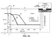
- FIG. 3A and 3B illustrate the evolution of B dopants (out-diffusion) from the source region 2 into the channel region 5 upon using a thermal budget of e.g. 350oC for a TFET with and without transition layer 7 in accordance with embodiments of the present invention.
- the thermal budget was applied to increase diffusion of the dopants (Boron), it is clear that the transition layer eliminates or at least drastically reduces the diffusion of the Boron dopants into the channel region 5.
- FIG. 3A It can be seen from FIG. 3A that, if the p+ doped source region 2 has a direct interface with the channel region 5, as illustrated by interface line 30, the source dopants out-diffuse into the channel region 5.
- graph 31 illustrates the dopant concentration in case a Boron doped Si source region 2 is in direct contact with an intrinsic Si channel region 5
- graph 32 illustrates the dopant concentration in case a Boron doped SiGe source region 2 is in direct contact with an intrinsic Si channel region 5
- graph 33 illustrates the dopant concentration in case a Boron doped Si 0.85 Ge 0.15 source region 2 is in direct contact with an intrinsic Si channel region 5.
- FIG. 3A Another situation illustrated in FIG. 3A is an embodiment of the present invention, where a Si 0.85 Ge 0.15 source region 2 ends at the location indicated by line 34. Between the source region 2 and the intrinsic Si channel region 5 a 10 nm thick undoped SiGe transition layer 7 is provided. It can be seen from graph 35 that the doping concentration has a steep profile in the transition layer 7. The profile illustrated in graph 35 shows a decay of about 16 decades over about 6 nm of the transition layer 7.
- FIG. 3B illustrates different dopant concentration graphs in function of transition layer 7 thickness.
- the Ge_SiGe curve 40 shows the Ge concentration with respect to position. In this way, the doping profile can be seen with respect to the material change.
- Graph 36 illustrates the dopant concentration for a Boron doped Si 0.85 Ge 0.15 source region 2 in case no transition layer 7 is present;
- graph 37 illustrates the dopant concentration for a Boron doped Si 0.85 Ge 0.15 source region 2 with a 2 nm thick transition layer 7;
- graph 38 illustrates the dopant concentration for a Boron doped Si 0.85 Ge 0.15 source region 2 with a 5 nm thick transition layer 7;
- graph 39 illustrates the dopant concentration for a Boron doped Si 0.85 Ge 0.15 source region 2 with a 10 nm thick transition layer 7. All the above graphs 36, 37, 38, 39 are measured at a thermal budget of growth of 750°C.
- transition layer 7 thicknesses between 2 nm and 5 nm are optimal. This result is specific for SiGe with 15% Ge. If full Ge is used, thicknesses between 2 nm and 10 nm, for example between 5 nm and 10 nm may be optimal.
- a processing method according to embodiments of the present invention is schematically illustrated in a flowchart 100 shown in FIG. 4 and will be described in detail below.
- the embodiment illustrated is for a nanostructure, e.g. nanowire TFET. It has, however, to be understood that this is only an example of a suitable method for forming a device according to embodiments of the present invention. The description of this particular embodiment is not intended to limit the present invention to the sequence of the process steps as described hereinafter.
- a substrate is provided (not illustrated in the drawings).
- said substrate may be a semiconductor substrate such as a silicon substrate or a silicon on insulator (SOI) substrate but any other suitable substrate can be used as well such as, for example, glass, ceramics, etc.
- a drain contact 8 is created in said substrate or alternatively on top of said substrate.
- the drain contact 8 may be made of a conductive material, e.g. said drain contact 8, may be a silicide containing structure (NiSi, CoSi 2 , TiSi 2 ...), a germanide containing structure, a metal containing structure, polysilicon or a combination thereof.
- drain contacts 8 formed of e.g.
- the drain contact 8 is a metal containing structure, all metals which form an ohmic contact with the material of a nanostructure, e.g. nanowire to be formed later on, should have a comparable work function with respect to the work function of the material of the nanostructure, e.g. nanowire.
- the drain contact 8 may be a silicide containing structure.
- the drain contact 8, can be the starting point for growing the nanostructure, e.g. nanowire and can, at the same time, act as the catalyst for the nanostructure, e.g. nanowire growth. However, the latter is not necessarily essential.
- the drain contact 8 cannot be used as a catalyst for the subsequent nanostructure, e.g. nanowire growth, a catalyst needs to be deposited onto the drain contact, step 111. Furthermore, the requirement of catalyst particles also depends on the technique used to form the nanostructure, e.g. nanowire.
- a nanostructure e.g. a nanowire is grown, e.g. by means of a VLS (Vapor-Liquid-Solid) process, but also any other suitable technique known by a person skilled in the art may be used to form the nanostructure, e.g. nanowire according to embodiments of the invention.
- the nanostructure, e.g. nanowire may be grown using techniques such as CVD (Chemical Vapour Deposition), MO-CVD (Metal Organic Chemical Vapour Deposition), or PECVD (plasma enhanced chemical vapour deposition) processes.
- CVD Chemical Vapour Deposition
- MO-CVD Metal Organic Chemical Vapour Deposition
- PECVD plasma enhanced chemical vapour deposition
- PLD Pulsed Laser Deposition
- ECD Electrochemical Deposition
- e-beam or MBE Molecular Beam Epitaxy
- the nanostructure e.g. nanowire
- different regions with different doping levels and different doping types need to be created to form the drain region 6, the channel region 5, the source region 2 and the transition layer 7 of the nanostructure, e.g. nanowire.
- the different regions in the nanostructure, e.g. nanowire can be doped during the growth process to obtain a n-type or p-type region.
- the doping of the different regions of the nanostructure, e.g. nanowire may be performed after growth of these regions by means of an additional doping step.
- the doping in one specific region, e.g. source region/drain region may for example be uniform, but may alternatively also have a non-uniform doping profile.
- a drain region 6 may be created.
- Said drain region 6 may be made of a first semiconductor material which is highly n doped in case of a p-type NW-TFET, or alternatively in case of a n-type NW-TFET said drain region 6 is highly p doped.
- the doping level of the drain region 6 may be in the range of 10 18 /cc to 10 21 /cc, for example in the range of 10 19 /cc to 5.10 20 /cc.
- the channel region 5 of the NW-TFET may be formed in the nanostructure, e.g. nanowire.
- Said channel region 5 may for example be made of the first semiconductor material, although other suitable/compatible materials can be used.
- the channel region may for example be lowly doped, e.g. having a doping level below 10 17 cm -3 or undoped.
- a transition layer 7 may be formed onto (above) the channel region 5.
- the transition layer 7 may be made of a material which is at least partly identical to the source semiconductor material to be applied later, and at least partly different from the channel semiconductor material.
- the transition layer material 7 has lower diffusion kinetics for the dopant of the source region 2 to be formed than the channel material.
- a source region 2 may be created onto the transition layer 7.
- Said source region 2 may be made of a second semiconductor material which is highly n doped in case of a n-type NW-TFET (or alternatively in case of a n-type NW-TFET said source region 2 is highly p doped).
- the doping level of the source region 2 may be in the range of 10 18 /cc to 10 21 /cc, for example in the range of 10 19 /cc to 5.10 20 /cc.
- a gate structure 4a+4b may be formed onto the sidewalls of the nanostructure, e.g. nanowire, more specifically at least onto the sidewalls of the channel region 5 of the nanostructure, e.g. nanowire.
- Said gate structure comprises a gate oxide 4a (also referred to as gate dielectric) and a gate electrode 4b (also referred to as gate contact).
- the gate oxide 4a is formed and deposited directly onto the channel region 5 of the nanostructure, e.g. nanowire.
- said gate oxide 4a completely covers the outer sidewalls of the channel region 5. To obtain a complete coverage of the channel region 5, a small overlap of the gate oxide 4a with the highly-doped drain region 6 and/or source region 2 may be desirable.
- a gate contact 4b (electrode) is deposited, step 114.
- said gate contact 4b may for example cover the whole gate oxide 4a.
- the gate dielectric 4a may for example be selected from at least one of silicon based oxide (e.g. silicon dioxide, silicon oxy nitride) aluminium oxide, high-k oxides (oxides, nitrided oxides), silicates and nitrided silicates of transition metals such as Hf, Ta, Ti, Nb, V, Y, Zr.
- silicon based oxide e.g. silicon dioxide, silicon oxy nitride
- high-k oxides oxides, nitrided oxides
- silicates and nitrided silicates of transition metals such as Hf, Ta, Ti, Nb, V, Y, Zr.
- said gate oxide 4a may be a high-k oxide such as hafnium oxide.
- the thickness of the gate oxide may for example be in the range of 0.5 nm to 20 nm.
- the gate contact 4b may for example be made of a conductive material, for example selected from at least one of poly silicon, poly germanium, metals such as Al, W, Ta, Ti, Ru, Pd, Rh, Re, Pt, and alloys thereof, metal-nitrides such as TaN and TiN, metal-silicon nitrides such as TaSiN, conductive oxides such as RuO 2 and ReO 3 , fully silicided metals (FUSI) such as CoSi 2 , NiSi and TiSi 2 , fully germanided metals (FUGE), workfunction tuneable metals, engineered materials to obtain a particular gate workfunction.
- said gate contact 4b may be made of a metal of which the workfunction has been engineered specifically for the chosen nanostructure, e.g. nanowire material, the gate oxide material and gate oxide thickness.
- an electrical contact 1 may be formed on the source region 2 (situated on top of the nanostructure, e.g. nanowire).
- Said electrical contact 1 may for example be made of a conductive material which is selected from at least one of a silicide containing structure (NiSi, CoSi 2 , TiSi 2 ,...), a germanide containing structure, a metal containing structure, poly silicon or a combination thereof.
- said electrical contact may be made of a combination of a metal with a silicide.
- an extra doping step may be advantageous.
- implantation of dopant elements followed by activation of the dopant elements by e.g. annealing can be applied to achieve n-type or p-type region in the nanostructure, e.g. nanowire.
- a layer, which is also referred to as dopant layer and which comprises dopant elements can be deposited or a dopant metal can be selectively deposited, e.g. with electrochemical deposition, onto the nanostructure, e.g. nanowire regions (not shown).
- An anneal step may then be applied so as to incorporate the dopant into the nanostructure, e.g. nanowire region, resulting in an n-type or p-type region.
Landscapes
- Insulated Gate Type Field-Effect Transistor (AREA)
- Thin Film Transistor (AREA)
Abstract
Description
- The present invention relates to the field of semiconductor devices and nanotechnology.
- More specifically, the invention relates to a nanostructure semiconductor device, more specifically to a tunnel field effect transistor having a segmented nanostructure (e.g. a heterostructure nanowire).
- Furthermore the invention relates to a method for manufacturing tunnel field effect transistor devices with integrated nanostructures such as nanowires having improved device properties.
- Microelectronic devices are generally fabricated on semiconductor substrates as integrated circuits. A complementary metal-oxide-semiconductor (CMOS) field effect transistor is one of the core elements of the integrated circuits. Dimensions and operating voltages of CMOS transistors are continuously reduced, or scaled down, to obtain ever-higher performance and packaging density of the integrated circuits.
- One of the problems due to the scaling down of CMOS transistors, is that the power consumption keeps increasing. This is partly because leakage currents are increasing (e.g. due to short channel effects) and because it becomes difficult to decrease the supply voltage. The latter is mainly due to the fact that the subthreshold slope is limited to minimally about 60 mV/decade, such that switching the transistor from ON to OFF needs a certain voltage variation and therefore a minimum supply voltage.
- Tunnel field-effect transistors (TFETs) are typically advertised as successors of metal-oxide semiconductor field-effect transistors (MOSFETs), because of their absence of short-channel effects and because of their resulting low off-currents. Another advantage of TFETs is that the subthreshold slope can be less than 60 mV/dec, the physical limit of conventional MOSFETs, such that potentially lower supply voltages can be used. However, TFETs typically suffer from low on-currents, a drawback related to the large resistance of the tunnel barrier.
- To increase the on-current of a silicon TFET, suggestions have been made in literature by Bhuwalka et al. (IEEE transactions on electron devices Vol. 52, ) to add a small (about 3 nm wide) section of highly-doped Si(1-x)Gex at the tunnel barrier. The Si(1-x)Gex has a smaller band gap than Si such that the effective tunnel barrier width decreases due to the presence of this section. However, these structures with the Si(1-x)Gex section can still not compete with conventional MOSFETs because of their low on-currents.
- Verhulst et al [A.S. Verhulst et al, J. Appl. Phys., 104(6):064514, 2008] have shown that the ON current of a tunnel field-effect transistor can be boosted by using a p-doped Ge (or p-doped SiGe) source in combination with a Si channel and n doped drain. However, the increase in ON current depends strongly on the abruptness of the (p) doping profile at the (Si)Ge/ intrinsic Si tunneling junction (see
FIG. 1 ). This is a challenging task to achieve, as the p -type dopants (e.g. B dopants) readily diffuse into the Si channel due to the thermal budget during the device fabrication. - It is an object of particular embodiments of the present invention to provide a method for achieving a tunnel Field Effect transistor (TFET) with a heterojunction thereby eliminating or at least reducing drastically the out-diffusion of the dopants of the source into the (intrinsic) channel region.
- It is another object of the present invention to provide a TFET with good properties, in particular for example a TFET with a high-quality heterojunction.
- The problem to be solved is avoiding out-diffusion of the dopants from the doped source towards the channel region such that a steep dopant profile is achieved at the interface of the source and channel. The problem of out diffusion especially occurs in heterostructures where the dopant of the source has lower diffusion kinetics in the channel material than in the source material. Since the doped source is in direct contact with the intrinsic channel, a source made of Ge (or SiGe) having dopants such as B which have higher diffusivity in Si compared to Ge (or SiGe) will always diffuse towards the Si channel, especially due to the thermal budget during fabrication of the TFET.
- The above objectives are accomplished by a method and a device according to embodiments of the present invention.
- Particular and preferred aspects of the invention are set out in the accompanying independent and dependent claims. Features from the dependent claims may be combined with features of the independent claims and with features of other independent claims as appropriate and not merely as explicitly set out in the claims.
- In a first aspect, embodiments of the present invention disclose a method for providing a tunnel field effect transistor (TFET) comprising at least a source region and a channel region, with a heterojunction between the source and the channel region, thereby eliminating or at least reducing drastically the out-diffusion of the dopants of the source into the (intrinsic) channel region. The method comprises at least the steps of:
- providing a substrate,
- providing onto said substrate a drain region made of a drain semiconductor material having a high doping level of e.g. 1018 cm-3 or higher,
- providing a channel region made of a channel semiconductor material onto said drain region, the channel region being lowly doped, e.g. having a doping level below 1017 cm-3, or undoped,
- providing a source region made of a source semiconductor material onto said channel region, and
- doping the source region and the drain region.
- A method according to embodiments the present invention has the advantage that the thickness of the transition layer can be engineered such that the transition layer coincides with a steep transition step from the doped source region to the lowly doped or undoped channel region, thereby maximizing the tunneling current.
- According to particular embodiments of the invention, doping the source region and the drain region comprises selectively doping the as-deposited source and drain regions to a desired doping level with a desired dopant type, for example 1018/cc to 1021/cc, to form a highly doped source and drain region, for example the doping level of the source region and/or the drain region may be in the range of 1019/cc to 5x10²⁰/cc. The dopant elements used for doping may be p-type dopants or alternatively n-type dopants. According to alternative embodiments, source and drain semiconductor material may be in situ doped during deposition.
- According to particular embodiments of the invention the semiconductor materials used in the TFET may be selected from at least one of group IV materials such as Si, Ge, C and binary compounds thereof, or group III/V materials such as In, Ga, As, Sb, Al, P, B, N and binary, tertiary and quaternary compounds thereof or group II/VI materials such as Cd, Zn, S, Se, Te, O and binary, tertiary and quaternary compounds thereof.
- According to particular embodiments of the invention said source semiconductor material may be germanium or Si(1-x)Gex with x > 0.15.
- According to particular embodiments of the invention said channel semiconductor material may be silicon.
- According to particular embodiments of the invention said transition layer is made of the source semiconductor material or a combination of the source and the channel semiconductor material. Dopants of the source region have higher diffusivity in the channel semiconductor material (e.g. Si) compared to their diffusivity in the source semiconductor material (e.g. Ge or SiGe).
- The sequence of the drain region, the channel region and the source region may lay in a longitudinal direction of the TFET. According to particular embodiments, the method for providing a tunnel field effect transistor (TFET) with a heterojunction may further comprise the steps of providing along the source-channel-drain regions a gate dielectric and a gate electrode, said gate dielectric covering along the longitudinal direction at least part of the source-channel-drain regions and said gate electrode being situated onto said gate dielectric, not extending beyond said gate dielectric, and the step of forming at least one source contact on the at least one source region.
- In alternative embodiments, a method according to embodiments of the present invention may comprise:
- providing a substrate with at least one drain contact
- providing on the drain contact a source-channel-drain structure made of at least two different semiconductor materials, said structure having at least one doped drain region, made of a first semiconductor material, at least one intrinsic channel region made of the first semiconductor material, and at least one highly doped source region made of a second semiconductor material different from the first semiconductor material, there being a source-channel interface and a drain-channel interface, the source-channel-drain structure having a longitudinal direction,
- providing a transition layer made of the second semiconductor material or a combination of the first and the second semiconductor material which is situated at the source-channel interface,
- providing on the source-channel-drain structure a gate dielectric, e.g. an oxide, and a gate electrode, said gate dielectric covering along the longitudinal direction at least part of the source-channel-drain structure and said gate electrode being situated on said gate dielectric, not extending beyond said gate dielectric, and
- forming at least one source contact on the at least one source region.
- According to particular embodiments, the source and drain regions are selectively doped to a desired doping level with a desired dopant type.
- According to particular embodiments, the gate dielectric and gate electrode form the gate structure and cover the source-channel-drain structure along the longitudinal direction thereof and extend at least up to the plane of the source-channel interface.
- According to particular embodiments, the first semiconductor material is selected from at least one of group IV materials such as Si, Ge, C and binary compounds thereof, or group III/V materials such as In, Ga, As, Sb, Al, P, B, N and binary, tertiary and quaternary compounds thereof or group II/VI materials such as Cd, Zn, S, Se, Te, O and binary, tertiary and quaternary compounds thereof. For example, the first semiconductor material may be silicon.
- According to particular embodiments, the second semiconductor material is selected from at least one of the group IV materials such as Si, Ge, C and binary compounds thereof, or group III/V materials such as In, Ga, As, Sb, Al, P, B, N and binary, tertiary and quaternary compounds thereof or group II/VI materials such as Cd, Zn, S, Se, Te, O and binary, tertiary and quaternary compounds thereof. For example, the second semiconductor material may be germanium or Si(1-x)Gex with x > 0.15.
- According to particular embodiments, the transition layer may be made of the second semiconductor material or a combination of the first and the second semiconductor material and wherein the dopants of the source region, such as e.g. B, have higher diffusivity in the first semiconductor material (e.g. Si) compared to their diffusivity in the second semiconductor material (e.g. Ge or SiGe).
- According to particular embodiments, the gate dielectric is selected from at least one of silicon based oxide (e.g. silicon dioxide, silicon oxy nitride) aluminium oxide, high-k oxides (oxides, nitrided oxides), silicates and nitrided silicates of transition metals such as Hf, Ta, Ti, Nb, V, Y, Zr. More particular the gate oxide may be a high-k oxide such as hafnium oxide.
- According to particular embodiments, the gate electrode (contact) is made of a conductive material and is selected from at least one of poly silicon, poly germanium, metals such as Al, W, Ta, Ti, Ru, Pd, Rh, Re, Pt, and alloys thereof, metal-nitrides such as TaN and TiN, metal-silicon nitrides such as TaSiN, conductive oxides such as RuO2 and ReO3, fully silicided metals (FUSI) such as CoSi2, NiSi and TiSi2, fully germanided metals (FUGE), workfunction tunable metals, engineered materials to obtain a particular gate workfunction. More particular the gate contact may be made of a metal of which the workfunction has been engineered specifically for the chosen TFET material (first and second semiconductor material).
- According to particular embodiments, said source and drain contacts may be made from a conductive material which is selected from at least one of a silicide containing structure (NiSi, CoSi2, TiSi2, ...), a germanide containing structure, a metal containing structure, poly silicon or a combination thereof. More particularly said source and drain may be a combination of a metal with a silicide.
- In a second aspect of the present invention, a heterostructure Tunnel Field Effect transistor (TFET) with a heterojunction is disclosed, which eliminates or at least drastically reduces the out-diffusion of the dopants of the source into the (intrinsic) channel region.
- In embodiments of this second aspect, a tunnel field effect transistor (TFET) is provided. Said TFET is a segmented hetero-TFET made of at least following segments (regions):
- A highly doped drain region made of a drain semiconductor material, e.g. with a doping level of 1018 cm-3 or higher,
- A channel region made of a lowly doped, e.g. doped at a doping level below 1017 cm-3, or undoped channel semiconductor material situated onto said drain region, and
- A doped source region made of a source semiconductor material onto said channel region.
- The TFET according to embodiments of the present invention may be a vertical device configuration and said vertical device may be of a nanostructure made of different segments (e.g. a segmented nanowire) wherein said segments form the source, channel and drain region of the TFET.
- According to particular embodiments a heterostructure TFET is disclosed in which at least the source and the channel of the TFET structure are made of different semiconducting materials. The invention has surprising benefits if the source of the TFET is made of a semiconductor material which is highly doped and the channel is made of another lowly doped, e.g. having a doping level below 1017 cm-3, or undoped semiconductor material and wherein a transition layer is placed in between the highly doped source and lowly doped or undoped channel. According to particular embodiments, significant surprising benefits are obtained if the source of the TFET is made of a Ge or SiGe semiconductor material which is highly doped, e.g. a highly doped Ge or SiGe with a Ge content higher than 15%, the channel is made of lowly doped, e.g. having a doping level below 1017 cm-3, or undoped Si semiconductor material and a Ge or SiGe transition layer is placed in between the highly doped source and lowly doped or undoped Si channel. The effect is most pronounced when the transition layer has higher Ge content (%). The effect of obtaining a steep doping profile is most pronounced if both a Ge source and Ge transition layer are used, such that the difference in dopant diffusivity with the Si channel is the largest. So also if a SiGe transition layer is used with a Ge source, the effect will be stronger if there is a higher Ge content in the transition layer. But also if a SiGe source and SiGe transition layer are used, the higher the Ge content the steeper the doping profile. Hence, in embodiments of the present invention it is especially the Ge content of the transition layer that matters. Alternatively, devices with a SiGe source, a Ge transition layer and a Si channel also result in a valuable device.
- Hence, in accordance with embodiments of the present invention, the problem of out-diffusion is solved by insertion of a transition layer in between the intrinsic channel and the doped source. The transition layer has a thickness of a few nm only, for example between 1 and 10 nm, depending on the choice of material for source region and channel region. A good choice is a thickness between 2 nm and 5 nm for a transistion layer made of SiGe with 15% Ge. The transition layer can contain the out-diffusion of dopants within a very limited region of a few nm, e.g. 1 to 10 nm, thus guaranteeing extremely good doping abruptness thanks to the lower diffusion of the dopants in the transition layer.
- According to particular embodiments of the present invention, the insertion of a transition layer between the source and the channel avoids the direct contact between the doped source and the intrinsic channel and allows preserving all of the dopants (e.g. B atoms) entirely within the source and transition layer.
- According to particular embodiments of the present invention, the insertion of a transition layer in a heterostructure TFET has the purpose of achieving an abrupt source-channel interface and to engineer the doping profile to coincide with the hetero-interface.
- According to particular embodiments of the invention, the segmented hetero-TFET is a vertical nanostructure, e.g. a nanowire wherein the different segments represent the source, channel and drain regions of the TFET.
- According to particular embodiments of the invention, the source and drain regions in the segmented hetero-TFET are selectively doped to a desired doping level with a desired dopant type, for example said source and drain regions may be selectively doped to a dopant concentration of 1018/cc to 1021/cc to form a highly doped source and drain region.
- According to particular embodiments of the invention, the semiconductor material of the hetero-TFET is selected from at least one of group IV materials such as Si, Ge, C and binary compounds thereof, or group III/V materials such as In, Ga, As, Sb, Al, P, B, N and binary, tertiary and quaternary compounds thereof or group II/VI materials such as Cd, Zn, S, Se, Te, O and binary, tertiary and quaternary compounds thereof.
- According to particular embodiments of the invention, the source semiconductor material of the hetero-TFET is made of germanium or Si(1-x)Gex with x > 0.15.
- According to particular embodiments of the invention, the channel semiconductor material of the hetero-TFET is made of silicon.
- According to particular embodiments of the invention, the transition layer of the hetero-TFET is made of the source semiconductor material or a combination of the source and the channel semiconductor material and wherein the dopants of the source have higher diffusivity in the channel semiconductor material (e.g. Si) compared to its diffusivity in the source semiconductor material (e.g. Ge or SiGe).
- According to particular embodiments, the TFET is a heterostructure TFET in which the source is made of highly doped Ge or SiGe with a p-type dopant selected from B, P,.. and the intrinsic channel is made of Si. The problem of out-diffusion of the p-type dopant towards the channel region is avoided by incorporation of a Ge or SiGe layer in between the source and channel region. Because the diffusion of p-type dopants such as B is much lower in Ge than in Si, the transition layer will act as a buffer layer. The thickness of said transition layer needs to be selected such that further diffusion of the dopant into the channel is eliminated.
- According to particular embodiments of the invention, the hetero-TFET comprises along the source-channel-drain regions a gate dielectric and a gate electrode. The sequence of the drain region, the channel region and the source region may lay in a longitudinal direction of the TFET. The gate dielectric covers along the longitudinal direction at least part of the source-channel-drain regions and said gate electrode is situated onto said gate dielectric, not extending beyond said gate dielectric. The TFET may furthermore comprise at least one source contact on the at least one source region.
- According to an alternative embodiment of the first or second aspect of the present invention, Carbon atoms may be added to the transition layer (or in other words added to the second semiconductor material or the combination of first and second semiconductor material) to further retard the out-diffusion of the dopants from the source region and further avoid diffusion of said dopants into the channel region. Furthermore the addition of carbon may reduce the compressive stress of the second semiconductor material on the first semiconductor material, e.g. the compressive stress of Ge on Si. Said addition of Carbon atoms (also referred to as carbon doping) is such that a concentration of 0 up to a maximum of 3 % carbon in the transition layer is achieved, for example not more than 2%.
- Furthermore a method for manufacturing a nanostructure (e.g. nanowire) TFET semiconductor device according to particular embodiments of the invention is disclosed. Said method comprises the steps of:
- providing on a substrate at least one drain contact onto which optionally a catalyst is deposited,
- growing a nanostructure, e.g. a nanowire, onto said substrate made of at least a first and a second semiconductor material, said nanostructure having an integrated drain region made of a first semiconductor material, an channel region made of the first semiconductor material, and a source region made of a second semiconductor material to form a TEFT structure, there being a source-channel interface and a drain-channel interface and,
- doping (selectively) said source region and drain region to a desired doping level and dopant type,
- depositing on at least part of the side walls of the nanostructure a gate dielectric (e.g. oxide),
- depositing on top of the gate dielectric (e.g. oxide) a gate electrode, said gate electrode being situated on said gate dielectric so as to not extend beyond said gate dielectric,
- forming a source contact at the source region of the nanostructure.
- With the term "nanostructure" is meant any two-dimensionally confined pieces of solid material in the form of wires (nanowires), tubes (nanotubes), rods (nanorods) and similar elongated substantially cylindrical or polygonal nanostructures having a longitudinal axis. A cross-dimension of the elongated nanostructures preferably lies in the range of 1 nm to 500 nm, in the range of 3 nm to 300 nm, or below 100 nm.
- According to particular embodiments of the present invention, the step of selectively doping said source region and drain region may be performed during the step of growing the nanostructure (nanowire) TFET.
- In a particular embodiment the doping level of the source region and drain region may be in the range of 1018/cc to 1021/cc to form a highly doped source and drain region, for example the doping level of the source region and drain region may be in the range of 1019/cc to 5x10²⁰/cc.
- According to particular embodiments, the TFET device may be made of a nanostructure e.g. a nanowire wherein said nanostructure forms the channel and potentially also the source and drain regions of the TFET. Alternatively, either the source or drain regions of the TFET are situated in the substrate whereby said substrate comprises highly doped regions acting as source and drain regions.
- According to particular embodiments, the diameter of the nanostructure (nanowire) TFET is between 1 and 500 nm and a length between 5 nm and 10 µm, for example a diameter between 2 nm and 200 nm and a length between 10 nm and 5 µm, e.g. between 10 nm and 1 µm.
- According to particular embodiments, the length of the channel region (referred to as Lchannel) is in the range of 5 nm to 10 µm, for example in the range of 10 nm to 5 µm.
- According to particular embodiments, the length of the transition layer is in the range of 1 nm to 10 nm, for example in the range of 2 nm to 5 nm. The optimal thickness of the transition layer depends on the composition of the transition layer and the thermal budget used during processing (influencing the mobility/diffusivity of the dopants). For example a good transition layer thickness for a SiGe (15% Ge) transition layer and thereby using a thermal budget during growth of around 750ºC is in the range of 2 nm to 5 nm.
- The above and other characteristics, features and advantages of the present invention will become apparent from the following detailed description, taken in conjunction with the accompanying drawings, which illustrate, by way of example, the principles of the invention. This description is given for the sake of example only, without limiting the scope of the invention, the scope of the invention being limited only by the claims. The reference figures quoted below refer to the attached drawings.
- All figures are intended to illustrate some aspects and particular embodiments of the present invention. The figures are depicted in a simplified way for reason of clarity. Not all alternatives and options are shown and therefore the invention is not limited to the content of the given drawings. Like numerals are employed to reference like parts in the different figures.
-
FIG. 1 illustrates that the increase in ON current strongly depends on the abruptness of the (p) doping profile at the (Si)Ge/ intrinsic Si tunneling junction. The legend illustrates the required thickness (nm) needed to reduce the dopant concentration by one decade in a Ge-source Si-channel TFET (whereby the doping gradient is illustrated within the Si channel). The curve with the highest ON-current is the curve with the most abrupt doping profile. -
FIG. 2A illustrates a state of the art TFET (NW-TFET) without a transition layer in between the source and channel region such that the dopants of the highly doped source region diffuse into the channel region leading to bad device characteristics.FIG. 2B illustrates the TFET (NW-TFET) according to particular embodiments of the invention whereby a transition layer is present in between the source and channel region such that the dopants of the highly doped source region cannot or not substantially diffuse into the channel region leading towards significantly improved device characteristics. -
FIG. 3A illustrates the evolution of the Boron out-diffusion from the B-doped source towards the intrinsic channel with and without the presence of a transition layer in accordance with embodiments of the present invention, upon high T activation step (900ºC). The transition layer used is a 10 nm undoped SiGe layer. -
FIG. 3B shows a graph illustrating the Boron out-diffusion for different transition layer thicknesses for SiGe (15% Ge) undergoing a thermal budget of growth at 750ºC. -
FIG. 4 illustrates a flow diagram of a particular method for fabricating a TFET (NW-TFET) according to embodiments of the present invention. - The present invention will be described with respect to particular embodiments and with reference to certain drawings but the invention is not limited thereto but only by the claims. The drawings described are only schematic and are non-limiting. In the drawings, the size of some of the elements may be exaggerated and not drawn on scale for illustrative purposes. The dimensions and the relative dimensions do not correspond to actual reductions to practice of the invention.
- Moreover, the term top and the like in the description and the claims are used for descriptive purposes and not necessarily for describing relative positions. It is to be understood that the terms so used are interchangeable under appropriate circumstances and that the particular embodiments described herein are capable of operation in other orientations than described or illustrated herein.
- It is to be noticed that the term "comprising", used in the claims, should not be interpreted as being restricted to the means listed thereafter; it does not exclude other elements or steps. It is thus to be interpreted as specifying the presence of the stated features, integers, steps or components as referred to, but does not preclude the presence or addition of one or more other features, integers, steps or components, or groups thereof. Thus, the scope of the expression "a device comprising means A and B" should not be limited to devices consisting only of components A and B. It means that with respect to the present invention, the only relevant components of the device are A and B.
- Reference throughout this specification to "one embodiment" or "an embodiment" means that a particular feature, structure or characteristic described in connection with the embodiment is included in at least one embodiment of the present invention. Thus, appearances of the phrases "in one embodiment" or "in an embodiment" in various places throughout this specification are not necessarily all referring to the same embodiment, but may. Furthermore, the particular features, structures or characteristics may be combined in any suitable manner, as would be apparent to one of ordinary skill in the art from this disclosure, in one or more embodiments.
- Similarly it should be appreciated that in the description of exemplary particular embodiments, various features of the invention are sometimes grouped together in a single embodiment, figure, or description thereof for the purpose of streamlining the disclosure and aiding in the understanding of one or more of the various inventive aspects. This method of disclosure, however, is not to be interpreted as reflecting an intention that the claimed invention requires more features than are expressly recited in each claim. Rather, as the following claims reflect, inventive aspects lie in less than all features of a single foregoing disclosed embodiment. Thus, the claims following the detailed description are hereby expressly incorporated into this detailed description, with each claim standing on its own as a separate embodiment of this invention.
- Furthermore, while some embodiments described herein include some but not other features included in other embodiments, combinations of features of different embodiments are meant to be within the scope of the invention, and form different embodiments, as would be understood by those in the art. For example, in the following claims, any of the claimed embodiments can be used in any combination.
- In the description provided herein, numerous specific details are set forth. However, it is understood that particular embodiments may be practiced without these specific details. In other instances, well-known methods, structures and techniques have not been shown in detail in order not to obscure an understanding of this description.
- The invention will now be described by a detailed description of several particular embodiments. It is clear that other particular embodiments can be configured according to the knowledge of persons skilled in the art without departing from the technical teaching of the invention as defined by the appended claims.
- Particular embodiments of the present invention provide a method to fabricate a hetero-junction in a Tunnel Field Effect Transistor (TFET) device configuration (e.g. in a segmented nanowire TFET). In prior art devices, since the highly doped source is in direct contact with the undoped channel, some amount of dopants will diffuse from the source into the channel, and this cannot be avoided due to the source deposition thermal budget. This out-diffusion reduces the steepness of the doping profile and hence deteriorates the device operation.
- Particular embodiments of the present invention comprise the insertion of a transition layer with a thickness of only a few nm in between the source and channel region such that the out-diffusion occurs within a very limited region of a few nm, not more than the thickness of the transition layer. The material of the transition layer is selected such that it has lower diffusion kinetics for the source dopants than the channel material, thus guaranteeing extremely good doping abruptness thanks to the lower diffusion of the dopants in the transition layer. The transition layer avoids the direct contact between the highly doped (e.g. Ge or SiGe) source and the undoped (e.g. Si) channel and allows to contain the whole doping (e.g. B atoms) entirely within the source region and transition layer. The thickness of the transition layer can be engineered such that the transition layer coincides with the steep transition step from the highly doped source region to the intrinsic region (channel), hence maximizing the tunneling current.
- At least some of the embodiments of the present invention relate to the creation of semiconductor devices and more specifically to the creation of a Tunnel-Field Effect Transistor, for example a nanostructure TFET (e.g. a Nanowire-TFET (NW-TFET)) on a semiconductor substrate. A heterostructure TFET (e.g. NW-TFET) is disclosed whereby the TFET is made of at least a first and second semiconductor material which comprises a drain region (section) made of a first semiconductor material or a second semiconductor material having a first doping level of at least 1018 cm-3 and first doping composition, a lowly doped, e.g. having a doping level below 1017 cm-3, or undoped channel region made of the first semiconductor material and a source region (section) made of the second semiconductor material having a second doping level and second doping composition. In particular embodiments, a p-doped section is situated at the one end of the TFET (NW-TFET), e.g. forming the source, and an n-doped section is situated in the other end of the TFET (NW-TFET), e.g. forming the drain.
- The TFET (NW-TFET) of embodiments of the present invention differs from all other state of the art TFET (NW-TFET) devices in the fact that a thin transition layer is situated at the interface of the highly doped source region, e.g. having a doping level of at least 1018 cm-3, and lowly doped, e.g. having a doping level below 1017 cm-3, or undoped channel region, the transition layer having a thickness of not more than 10 nm, wherein said transition layer is made of a material which is at least partly identical to the source semiconductor material and at least partly different from the channel semiconductor material and which has lower diffusion kinetics for the dopant than the channel material.
- The resulting TFET (NW-TFET) according to embodiments of the present invention has an improved performance, more specifically an improved tunneling efficiency compared to similar state of the art TFET devices without a transition layer. This is because the TFET according to embodiments of the present invention has a much sharper (steeper) doping profile and because of the coincidence of the heterojunction with the sharp doping transition (achieving a well-defined tunneling location).
- The TFET (NW-TFET) of some embodiments of the invention can further be characterized as a TFET having at least one nanostructure (nanowire). Said nanostructure comprises the source region, channel region and drain region of the TFET device as well as the novel transition layer according to embodiments of the present invention, being situated at the interface between the source and channel region. More specifically, in embodiments of the present invention said transition layer is situated in between the source region and the channel region of the nanostructure. The purpose of the transition layer is to get a well-defined tunneling region after the full fabrication process of the TFET.
- The nanostructure (nanowire) in the TFET of some embodiments of the present invention can be characterized as a semiconducting nanowire wherein the diameter of the nanowire is between 1 and 500 nm and the length of the nanowire is between 5 nm and 2 µm. In particular embodiments, the diameter of the nanowire may be between 2 nm and 200 nm and the length of the nanowire may be between 10 nm and 1 µm.
-
FIG. 2A illustrates a cross-section of a state of the art TFET (NW-TFET) without a transition layer in between thesource 2 andchannel 5 region such that the dopants 3 of the highlydoped source 2 region diffuse into thechannel 5 region leading towards bad device characteristics.FIG. 2B illustrates the TFET (NW-TFET) according to particular embodiments of the invention whereby atransition layer 7 is present in between thesource 2 andchannel 5 region such that the dopants of the highlydoped source region 2 cannot diffuse into thechannel region 5 leading towards significantly improved device characteristics. - According to particular embodiments as illustrated in
FIG. 2B , a TFET according to embodiments of the invention is made of a segmented hetero-TFET made of at least adoped drain region 6 made of a drain semiconductor material, e.g. having a doping level of at least 1018 cm-3, a lowly doped, e.g. having a doping level below 1017 cm-3 orundoped channel region 5 made of a channel semiconductor material situated onto saiddrain region 6, adoped source region 2 made of a source semiconductor material onto saidchannel region 5 and further comprising atransition layer 7 made of a material which is at least partly identical to the source semiconductor material and at least partly different from the channel semiconductor material and which is situated in between saidchannel region 5 and saiddoped source region 2. - According to particular embodiments of the invention, the segmented hetero-TFET is a vertical nanostructure e.g. a nanowire wherein the different segments represent the source, channel and drain regions of the TFET.
- According to particular embodiments of the invention, the
source 2 and drain 6 regions in the segmented hetero-TFET are selectively doped to a predetermined, desired, doping level with a predetermined, desired, dopant type, for example said source and drain regions are selectively doped to a dopant concentration of 1018/cc to 1021/cc to form a highlydoped source region 2 and drainregion 6. - According to particular embodiments of the invention, the semiconductor materials used in the hetero-TFET are selected from at least one of group IV materials such as Si, Ge, C and binary compounds thereof, or group III/V materials such as In, Ga, As, Sb, Al, P, B, N and binary, tertiary and quaternary compounds thereof or group II/VI materials such as Cd, Zn, S, Se, Te, O and binary, tertiary and quaternary compounds thereof.
- According to particular embodiments of the invention, the source semiconductor material of the hetero-TFET may be germanium or Si(1-x)Gex with x > 0.15.
- According to particular embodiments of the invention, the channel semiconductor material of the hetero-TFET may be silicon.
- According to particular embodiments of the invention, the
transition layer 7 of the hetero-TFET is made of the source semiconductor material or a combination of the source and the channel semiconductor material. Thetransition layer 7 material is selected such that the dopants of thesource 2 have higher diffusivity in the channel semiconductor material 5 (e.g. Si) compared to their diffusivity in the source semiconductor material 2 (e.g. Ge or SiGe). - According to particular embodiments of the invention, the hetero-TFET comprises along the source-channel-
drain regions gate dielectric 4a and agate electrode 4b, saidgate dielectric 4a covering along the longitudinal direction L of the TFET at least part of the source-channel-drain regions gate electrode 4b being situated onto saidgate dielectric 4a, not extending beyond saidgate dielectric 4a. Thesource region 2 may furthermore comprise at least onesource contact 1. -
FIG. 3A and3B illustrate the evolution of B dopants (out-diffusion) from thesource region 2 into thechannel region 5 upon using a thermal budget of e.g. 350ºC for a TFET with and withouttransition layer 7 in accordance with embodiments of the present invention. The thermal budget was applied to increase diffusion of the dopants (Boron), it is clear that the transition layer eliminates or at least drastically reduces the diffusion of the Boron dopants into thechannel region 5. - It can be seen from
FIG. 3A that, if the p+ dopedsource region 2 has a direct interface with thechannel region 5, as illustrated byinterface line 30, the source dopants out-diffuse into thechannel region 5. Different situations are illustrated inFIG. 3A :graph 31 illustrates the dopant concentration in case a Boron dopedSi source region 2 is in direct contact with an intrinsicSi channel region 5;graph 32 illustrates the dopant concentration in case a Boron dopedSiGe source region 2 is in direct contact with an intrinsicSi channel region 5;graph 33 illustrates the dopant concentration in case a Boron doped Si0.85Ge0.15 source region 2 is in direct contact with an intrinsicSi channel region 5. - Another situation illustrated in
FIG. 3A is an embodiment of the present invention, where a Si0.85Ge0.15 source region 2 ends at the location indicated byline 34. Between thesource region 2 and the intrinsic Si channel region 5 a 10 nm thick undopedSiGe transition layer 7 is provided. It can be seen from graph 35 that the doping concentration has a steep profile in thetransition layer 7. The profile illustrated in graph 35 shows a decay of about 16 decades over about 6 nm of thetransition layer 7. -
FIG. 3B illustrates different dopant concentration graphs in function oftransition layer 7 thickness. The B_SiGE... curves illustrate the B-concentration (= doping concentration) with respect to position. TheGe_SiGe curve 40 shows the Ge concentration with respect to position. In this way, the doping profile can be seen with respect to the material change.Graph 36 illustrates the dopant concentration for a Boron doped Si0.85Ge0.15 source region 2 in case notransition layer 7 is present;graph 37 illustrates the dopant concentration for a Boron doped Si0.85Ge0.15 source region 2 with a 2 nmthick transition layer 7;graph 38 illustrates the dopant concentration for a Boron doped Si0.85Ge0.15 source region 2 with a 5 nmthick transition layer 7; andgraph 39 illustrates the dopant concentration for a Boron doped Si0.85Ge0.15 source region 2 with a 10 nmthick transition layer 7. All theabove graphs graphs embodiment transition layer 7 thicknesses between 2 nm and 5 nm are optimal. This result is specific for SiGe with 15% Ge. If full Ge is used, thicknesses between 2 nm and 10 nm, for example between 5 nm and 10 nm may be optimal. - A processing method according to embodiments of the present invention is schematically illustrated in a
flowchart 100 shown inFIG. 4 and will be described in detail below. The embodiment illustrated is for a nanostructure, e.g. nanowire TFET. It has, however, to be understood that this is only an example of a suitable method for forming a device according to embodiments of the present invention. The description of this particular embodiment is not intended to limit the present invention to the sequence of the process steps as described hereinafter. - In a
first step 110, a substrate is provided (not illustrated in the drawings). For example said substrate may be a semiconductor substrate such as a silicon substrate or a silicon on insulator (SOI) substrate but any other suitable substrate can be used as well such as, for example, glass, ceramics, etc. According to an embodiment of the invention, in said substrate or alternatively on top of said substrate, adrain contact 8 is created. Thedrain contact 8 may be made of a conductive material, e.g. saiddrain contact 8, may be a silicide containing structure (NiSi, CoSi2, TiSi2...), a germanide containing structure, a metal containing structure, polysilicon or a combination thereof. Also disclosed aredrain contacts 8 formed of e.g. conductive oxides and even conductive polymers. In case thedrain contact 8 is a metal containing structure, all metals which form an ohmic contact with the material of a nanostructure, e.g. nanowire to be formed later on, should have a comparable work function with respect to the work function of the material of the nanostructure, e.g. nanowire. As an example only, thedrain contact 8 may be a silicide containing structure. Thedrain contact 8, can be the starting point for growing the nanostructure, e.g. nanowire and can, at the same time, act as the catalyst for the nanostructure, e.g. nanowire growth. However, the latter is not necessarily essential. - In case the
drain contact 8 cannot be used as a catalyst for the subsequent nanostructure, e.g. nanowire growth, a catalyst needs to be deposited onto the drain contact,step 111. Furthermore, the requirement of catalyst particles also depends on the technique used to form the nanostructure, e.g. nanowire. - In a
next step 112, a nanostructure, e.g. a nanowire is grown, e.g. by means of a VLS (Vapor-Liquid-Solid) process, but also any other suitable technique known by a person skilled in the art may be used to form the nanostructure, e.g. nanowire according to embodiments of the invention. For example, the nanostructure, e.g. nanowire may be grown using techniques such as CVD (Chemical Vapour Deposition), MO-CVD (Metal Organic Chemical Vapour Deposition), or PECVD (plasma enhanced chemical vapour deposition) processes. Alternatively, also PLD (Pulsed Laser Deposition), ECD (Electrochemical Deposition), e-beam or MBE (Molecular Beam Epitaxy) processes may be used to grow the nanostructure, e.g. nanowire. - During growth of the nanostructure, e.g. nanowire, different regions with different doping levels and different doping types need to be created to form the
drain region 6, thechannel region 5, thesource region 2 and thetransition layer 7 of the nanostructure, e.g. nanowire. The different regions in the nanostructure, e.g. nanowire, can be doped during the growth process to obtain a n-type or p-type region. Alternatively, the doping of the different regions of the nanostructure, e.g. nanowire may be performed after growth of these regions by means of an additional doping step. The doping in one specific region, e.g. source region/drain region may for example be uniform, but may alternatively also have a non-uniform doping profile. - During growth of the nanostructure, e.g. nanowire, first a
drain region 6 may be created. Saiddrain region 6 may be made of a first semiconductor material which is highly n doped in case of a p-type NW-TFET, or alternatively in case of a n-type NW-TFET saiddrain region 6 is highly p doped. The doping level of thedrain region 6 may be in the range of 1018/cc to 1021/cc, for example in the range of 1019/cc to 5.1020/cc. - Subsequently, the
channel region 5 of the NW-TFET may be formed in the nanostructure, e.g. nanowire. Saidchannel region 5 may for example be made of the first semiconductor material, although other suitable/compatible materials can be used. The channel region may for example be lowly doped, e.g. having a doping level below 1017 cm-3 or undoped. - In a next step, a
transition layer 7 may be formed onto (above) thechannel region 5. Thetransition layer 7 may be made of a material which is at least partly identical to the source semiconductor material to be applied later, and at least partly different from the channel semiconductor material. Thetransition layer material 7 has lower diffusion kinetics for the dopant of thesource region 2 to be formed than the channel material. - In a next step, a
source region 2 may be created onto thetransition layer 7.Said source region 2 may be made of a second semiconductor material which is highly n doped in case of a n-type NW-TFET (or alternatively in case of a n-type NW-TFET saidsource region 2 is highly p doped). The doping level of thesource region 2 may be in the range of 1018/cc to 1021/cc, for example in the range of 1019/cc to 5.1020/cc. - In a
next step gate structure 4a+4b may be formed onto the sidewalls of the nanostructure, e.g. nanowire, more specifically at least onto the sidewalls of thechannel region 5 of the nanostructure, e.g. nanowire. Said gate structure comprises agate oxide 4a (also referred to as gate dielectric) and agate electrode 4b (also referred to as gate contact). First thegate oxide 4a is formed and deposited directly onto thechannel region 5 of the nanostructure, e.g. nanowire. In particular embodiments, saidgate oxide 4a completely covers the outer sidewalls of thechannel region 5. To obtain a complete coverage of thechannel region 5, a small overlap of thegate oxide 4a with the highly-dopeddrain region 6 and/orsource region 2 may be desirable. - Onto the
gate dielectric 4a, e.g. gate oxide, agate contact 4b (electrode) is deposited,step 114. saidgate contact 4b may for example cover thewhole gate oxide 4a. - The
gate dielectric 4a may for example be selected from at least one of silicon based oxide (e.g. silicon dioxide, silicon oxy nitride) aluminium oxide, high-k oxides (oxides, nitrided oxides), silicates and nitrided silicates of transition metals such as Hf, Ta, Ti, Nb, V, Y, Zr. In particular embodiments, saidgate oxide 4a may be a high-k oxide such as hafnium oxide. The thickness of the gate oxide may for example be in the range of 0.5 nm to 20 nm. - The
gate contact 4b may for example be made of a conductive material, for example selected from at least one of poly silicon, poly germanium, metals such as Al, W, Ta, Ti, Ru, Pd, Rh, Re, Pt, and alloys thereof, metal-nitrides such as TaN and TiN, metal-silicon nitrides such as TaSiN, conductive oxides such as RuO2 and ReO3, fully silicided metals (FUSI) such as CoSi2, NiSi and TiSi2, fully germanided metals (FUGE), workfunction tuneable metals, engineered materials to obtain a particular gate workfunction. In particular embodiments, saidgate contact 4b may be made of a metal of which the workfunction has been engineered specifically for the chosen nanostructure, e.g. nanowire material, the gate oxide material and gate oxide thickness. - Finally, as illustrated in
step 115, anelectrical contact 1 may be formed on the source region 2 (situated on top of the nanostructure, e.g. nanowire). Saidelectrical contact 1 may for example be made of a conductive material which is selected from at least one of a silicide containing structure (NiSi, CoSi2, TiSi2,...), a germanide containing structure, a metal containing structure, poly silicon or a combination thereof. In particular embodiments, said electrical contact may be made of a combination of a metal with a silicide. - In case the nanostructure, e.g. nanowire, in particular the source and drain thereof, is not doped during the growth process, an extra doping step may be advantageous. For example, implantation of dopant elements followed by activation of the dopant elements by e.g. annealing can be applied to achieve n-type or p-type region in the nanostructure, e.g. nanowire. Alternatively, a layer, which is also referred to as dopant layer and which comprises dopant elements can be deposited or a dopant metal can be selectively deposited, e.g. with electrochemical deposition, onto the nanostructure, e.g. nanowire regions (not shown). An anneal step may then be applied so as to incorporate the dopant into the nanostructure, e.g. nanowire region, resulting in an n-type or p-type region.
- It is to be understood that although particular embodiments, specific constructions and configurations, as well as materials, have been discussed herein for devices according to the present invention, various changes or modifications in form and detail may be made without departing from the scope of this invention as defined by the appended claims.
Claims (15)
- A method for providing a tunnel field effect transistor (TFET) with a hetero-junction, said method comprising at least the steps of:- providing a substrate,- providing onto said substrate a drain region (6) made of a drain semiconductor material,- providing a channel region (5) made of a lowly doped or undoped channel semiconductor material onto said drain region (6),- providing a source region (2) made of a source semiconductor material onto said channel region, and- doping the source region (2) and the drain region (6),
the method being characterized in that before providing the source region (2) a transition layer (7) is provided made of a material which is at least partly identical to the source semiconductor material and at least partly different from the channel semiconductor material and which has lower diffusion kinetics for the dopants of the source region (2) than the channel material. - The method of claim 1 wherein doping the source region (2) and the drain region (6) comprises selectively doping these regions to a pre-determined doping level with a pre-determined dopant type.
- The method according to claim 2, wherein doping the source region (2) and the drain region (6) comprises doping these regions to a dopant concentration of 1018/cc to 1021/cc.
- The method of any of the foregoing claims wherein providing a drain region (6), a channel region (5) and/or a source region (2) comprises selecting semiconductor material from at least one of group IV materials and binary compounds thereof, group III/V materials and binary, tertiary and quaternary compounds thereof or group II/VI materials and binary, tertiary and quaternary compounds thereof.
- The method of claim 4 wherein providing a source region (2) comprises selecting germanium or Si(1-x)Gex with x > 0.15 as source semiconductor material.
- The method of claim 4, wherein providing a channel region (5) comprises selecting silicon as channel semiconductor material.
- The method of any of foregoing claims wherein providing the transition layer (7) comprises providing the transition layer (7) made of the source semiconductor material or a combination of the source and the channel semiconductor material.
- The method of any of foregoing claims, wherein the drain region (6), the channel region (5) and the source region (2) lay in a longitudinal direction (L) of the TFET, the method further comprising the steps of:- providing along the source-channel-drain regions a gate dielectric (4a) and a gate electrode (4b), said gate dielectric (4a) covering along the longitudinal direction (L) at least part of the source-channel-drain regions and said gate electrode (4b) being situated onto said gate dielectric (4a), not extending beyond said gate dielectric (4a), and- forming at least one source contact (1) on the at least one source region (2).
- The method of any of foregoing claims, furthermore comprising adding carbon atoms to said transition layer (7), said addition of carbon atoms being such that a concentration of 0 up to a maximum of 3 % carbon in the transition layer is achieved.
- A tunnel field effect transistor (TFET) comprising at least following segments:- a doped drain region (6) made of a drain semiconductor material,- a channel region (5) made of a lowly doped or undoped channel semiconductor material situated onto said drain region (6),- a doped source region (2) made of a source semiconductor material onto said channel region (5),
characterized in that a transition layer (7) made of a material which is at least partly identical to the source semiconductor material and at least partly different from the channel semiconductor material is situated in between said channel region (5) and said doped source region (2). - The TFET of claim 10 wherein the TFET is a segmented vertical nanostructure having a diameter between 1 and 500 nm and a length between 5 nm and 2 µm.
- The TFET of any of claims 10 or 11, wherein the transition layer has a thickness of not more than 10 nm.
- The TFET of any of foregoing claims 10 to 12, the drain region (6), channel region (5) and source region (2) lying in a longitudinal direction (L) of the TFET wherein on the source-channel-drain structure a gate dielectric (4a) and a gate electrode (4b) are provided, said gate dielectric (4a) covering along the longitudinal direction at least part of the source-channel-drain structure and said gate electrode being situated on said gate dielectric, not extending beyond said gate dielectric.
- The TFET of any of foregoing claims 10 to 13, wherein said transition layer (7) is made of the source semiconductor material or a combination of the source and the channel semiconductor material.
- The TFET of any of foregoing claims 10 to 14, further comprising at least one source contact on the at least one source region (2).
Applications Claiming Priority (1)
| Application Number | Priority Date | Filing Date | Title |
|---|---|---|---|
| US22009509P | 2009-06-24 | 2009-06-24 |
Publications (2)
| Publication Number | Publication Date |
|---|---|
| EP2267782A2 true EP2267782A2 (en) | 2010-12-29 |
| EP2267782A3 EP2267782A3 (en) | 2013-03-13 |
Family
ID=43027634
Family Applications (1)
| Application Number | Title | Priority Date | Filing Date |
|---|---|---|---|
| EP10166385A Withdrawn EP2267782A3 (en) | 2009-06-24 | 2010-06-17 | Control of tunneling junction in a hetero tunnel field effect transistor |
Country Status (2)
| Country | Link |
|---|---|
| US (2) | US8241983B2 (en) |
| EP (1) | EP2267782A3 (en) |
Cited By (2)
| Publication number | Priority date | Publication date | Assignee | Title |
|---|---|---|---|---|
| GB2518679A (en) * | 2013-09-30 | 2015-04-01 | Ibm | Reconfigurable tunnel field-effect transistors |
| US9245989B2 (en) | 2011-12-19 | 2016-01-26 | Intel Corporation | High voltage field effect transistors |
Families Citing this family (22)
| Publication number | Priority date | Publication date | Assignee | Title |
|---|---|---|---|---|
| CN101901837A (en) * | 2010-06-24 | 2010-12-01 | 复旦大学 | A gate-controlled PN field effect transistor and its control method |
| US8890118B2 (en) * | 2010-12-17 | 2014-11-18 | Intel Corporation | Tunnel field effect transistor |
| US8629480B2 (en) * | 2011-05-27 | 2014-01-14 | The United States Of America As Represented By The Secretary Of The Army | Hetero-junction tunneling transistor |
| JP2013038336A (en) * | 2011-08-10 | 2013-02-21 | Toshiba Corp | Semiconductor device |
| US8890119B2 (en) * | 2012-12-18 | 2014-11-18 | Intel Corporation | Vertical nanowire transistor with axially engineered semiconductor and gate metallization |
| US9209288B2 (en) * | 2012-12-21 | 2015-12-08 | Intel Corporation | Reduced scale resonant tunneling field effect transistor |
| CN103151391B (en) * | 2013-03-18 | 2015-08-12 | 北京大学 | The short grid tunneling field-effect transistor of vertical non-uniform doped channel and preparation method |
| EP3123520A4 (en) * | 2014-03-28 | 2017-11-22 | Intel Corporation | Selectively regrown top contact for vertical semiconductor devices |
| EP2993696B1 (en) | 2014-09-02 | 2020-08-05 | IMEC vzw | Heterosection tunnel field-effect transistor (TFET) |
| EP3010044B1 (en) * | 2014-10-13 | 2019-02-13 | IMEC vzw | Layered structure of a p-TFET |
| US10236345B2 (en) | 2015-06-22 | 2019-03-19 | Intel Corporation | Field effect transistor having a Fermi filter between a source and source contact thereof |
| US9548381B1 (en) * | 2015-12-14 | 2017-01-17 | Globalfoundries Inc. | Method and structure for III-V nanowire tunnel FETs |
| US10833193B2 (en) | 2016-09-30 | 2020-11-10 | Institute of Microelectronics, Chinese Academy of Sciences | Semiconductor device, method of manufacturing the same and electronic device including the device |
| CN106298778A (en) | 2016-09-30 | 2017-01-04 | 中国科学院微电子研究所 | Semiconductor device, manufacturing method thereof, and electronic equipment including the same |
| US10276714B2 (en) * | 2017-08-09 | 2019-04-30 | International Business Machines Corporation | Twin gate field effect diode |
| KR102314006B1 (en) * | 2017-09-11 | 2021-10-18 | 삼성전자주식회사 | Vertical field effect transistor and semiconductor device including the same |
| CN108074979A (en) * | 2017-11-30 | 2018-05-25 | 中国科学院上海微系统与信息技术研究所 | Field-effect transistor, biosensor based on vertical tunnelling and preparation method thereof |
| US10355046B1 (en) * | 2017-12-29 | 2019-07-16 | Spin Memory, Inc. | Steep slope field-effect transistor (FET) for a perpendicular magnetic tunnel junction (PMTJ) |
| WO2020076759A1 (en) | 2018-10-09 | 2020-04-16 | Micron Technology, Inc. | Transistors including heterogeneous channels, and related devices, electronic systems, and methods |
| US11211487B2 (en) | 2019-08-15 | 2021-12-28 | Micron Technology, Inc. | Transistors, memory structures and memory arrays containing two-dimensional materials between a source/drain region and a channel region |
| US20230268410A1 (en) * | 2022-02-22 | 2023-08-24 | Intel Corporation | Vertical tunneling field-effect transistor |
| CN115528104A (en) * | 2022-10-08 | 2022-12-27 | 西安邮电大学 | A dual-gate tunneling field-effect transistor based on a dual-material gate dielectric |
Family Cites Families (16)
| Publication number | Priority date | Publication date | Assignee | Title |
|---|---|---|---|---|
| US4994868A (en) * | 1988-12-06 | 1991-02-19 | Itt Corporation | Heterojunction confined channel FET |
| EP0809865B1 (en) | 1995-12-15 | 2000-07-12 | Koninklijke Philips Electronics N.V. | SEMICONDUCTOR FIELD EFFECT DEVICE COMPRISING A SiGe LAYER |
| US6723621B1 (en) * | 1997-06-30 | 2004-04-20 | International Business Machines Corporation | Abrupt delta-like doping in Si and SiGe films by UHV-CVD |
| US7297990B1 (en) * | 1999-05-07 | 2007-11-20 | The Ohio State University | Si/SiGe interband tunneling diode structures including SiGe diffusion barriers |
| US6706542B1 (en) * | 2000-01-07 | 2004-03-16 | Triquint Technology Holding Co. | Application of InAIAs double-layer to block dopant out-diffusion in III-V device Fabrication |
| US6316795B1 (en) | 2000-04-03 | 2001-11-13 | Hrl Laboratories, Llc | Silicon-carbon emitter for silicon-germanium heterojunction bipolar transistors |
| US6362065B1 (en) * | 2001-02-26 | 2002-03-26 | Texas Instruments Incorporated | Blocking of boron diffusion through the emitter-emitter poly interface in PNP HBTs through use of a SiC layer at the top of the emitter epi layer |
| US6670654B2 (en) * | 2002-01-09 | 2003-12-30 | International Business Machines Corporation | Silicon germanium heterojunction bipolar transistor with carbon incorporation |
| FR2868207B1 (en) * | 2004-03-25 | 2006-09-08 | Commissariat Energie Atomique | FIELD EFFECT TRANSISTOR WITH MATERIALS OF SOURCE, DRAIN AND ADAPTED CHANNEL AND INTEGRATED CIRCUIT COMPRISING SUCH A TRANSISTOR |
| US20060091490A1 (en) * | 2004-11-03 | 2006-05-04 | Hung-Wei Chen | Self-aligned gated p-i-n diode for ultra-fast switching |
| US7271457B2 (en) | 2005-03-04 | 2007-09-18 | Bae Systems Information And Electronic Systems Integration Inc. | Abrupt channel doping profile for fermi threshold field effect transistors |
| US8018003B2 (en) * | 2005-05-27 | 2011-09-13 | Synopsys, Inc. | Leakage power reduction in CMOS circuits |
| US20070148939A1 (en) * | 2005-12-22 | 2007-06-28 | International Business Machines Corporation | Low leakage heterojunction vertical transistors and high performance devices thereof |
| US7893476B2 (en) * | 2006-09-15 | 2011-02-22 | Imec | Tunnel effect transistors based on silicon nanowires |
| US20080308904A1 (en) * | 2007-06-15 | 2008-12-18 | Texas Instruments Incorporated | P-doped region with improved abruptness |
| US8026509B2 (en) * | 2008-12-30 | 2011-09-27 | Intel Corporation | Tunnel field effect transistor and method of manufacturing same |
-
2010
- 2010-06-17 EP EP10166385A patent/EP2267782A3/en not_active Withdrawn
- 2010-06-22 US US12/820,681 patent/US8241983B2/en active Active
-
2012
- 2012-07-25 US US13/558,184 patent/US8431924B2/en active Active
Non-Patent Citations (2)
| Title |
|---|
| A.S. VERHULST ET AL., J. APPL. PHYS., vol. 104, no. 6, 2008, pages 064514 |
| BHUWALKA ET AL., IEEE TRANSACTIONS ON ELECTRON DEVICES, vol. 52, no. 7, July 2005 (2005-07-01) |
Cited By (5)
| Publication number | Priority date | Publication date | Assignee | Title |
|---|---|---|---|---|
| US9245989B2 (en) | 2011-12-19 | 2016-01-26 | Intel Corporation | High voltage field effect transistors |
| US9685508B2 (en) | 2011-12-19 | 2017-06-20 | Intel Corporation | High voltage field effect transistors |
| US10263074B2 (en) | 2011-12-19 | 2019-04-16 | Intel Corporation | High voltage field effect transistors |
| GB2518679A (en) * | 2013-09-30 | 2015-04-01 | Ibm | Reconfigurable tunnel field-effect transistors |
| US9293467B2 (en) | 2013-09-30 | 2016-03-22 | Globalfoundries Inc. | Reconfigurable tunnel field-effect transistors |
Also Published As
| Publication number | Publication date |
|---|---|
| US8241983B2 (en) | 2012-08-14 |
| EP2267782A3 (en) | 2013-03-13 |
| US20100327319A1 (en) | 2010-12-30 |
| US8431924B2 (en) | 2013-04-30 |
| US20120298961A1 (en) | 2012-11-29 |
Similar Documents
| Publication | Publication Date | Title |
|---|---|---|
| US8431924B2 (en) | Control of tunneling junction in a hetero tunnel field effect transistor | |
| EP2309544B1 (en) | Tunnel field effect transistor with improved subthreshold swing | |
| US8148220B2 (en) | Tunnel effect transistors based on elongate monocrystalline nanostructures having a heterostructure | |
| US8120115B2 (en) | Tunnel field-effect transistor with gated tunnel barrier | |
| US7893476B2 (en) | Tunnel effect transistors based on silicon nanowires | |
| US9318583B2 (en) | Tunnel field effect transistor and method for making thereof | |
| US8629428B2 (en) | Line-tunneling tunnel field-effect transistor (TFET) and manufacturing method | |
| EP1901354B1 (en) | A tunnel field-effect transistor with gated tunnel barrier | |
| US20080318385A1 (en) | Tunneling field effect transistor using angled implants for forming asymmetric source/drain regions | |
| JP5171161B2 (en) | Nanowire tunnel field effect transistor semiconductor device and manufacturing method thereof | |
| CN102272933A (en) | Tunnel field effect transistor and method of manufacturing same | |
| WO2012152762A1 (en) | Tunnel field effect transistor device | |
| JP2009524923A (en) | Tunnel transistor with barrier | |
| US20080315183A1 (en) | Semiconductor device with carbon nanotube channel and manufacturing method thereof | |
| US8872230B2 (en) | Tunnel field-effect transistor and methods for manufacturing thereof | |
| EP1901355B1 (en) | Tunnel effect transistors based on monocrystalline nanowires having a heterostructure | |
| HK1175887B (en) | Techniques for forming contacts to quantum well transistors |
Legal Events
| Date | Code | Title | Description |
|---|---|---|---|
| PUAI | Public reference made under article 153(3) epc to a published international application that has entered the european phase |
Free format text: ORIGINAL CODE: 0009012 |
|
| AK | Designated contracting states |
Kind code of ref document: A2 Designated state(s): AL AT BE BG CH CY CZ DE DK EE ES FI FR GB GR HR HU IE IS IT LI LT LU LV MC MK MT NL NO PL PT RO SE SI SK SM TR |
|
| AX | Request for extension of the european patent |
Extension state: BA ME RS |
|
| PUAL | Search report despatched |
Free format text: ORIGINAL CODE: 0009013 |
|
| AK | Designated contracting states |
Kind code of ref document: A3 Designated state(s): AL AT BE BG CH CY CZ DE DK EE ES FI FR GB GR HR HU IE IS IT LI LT LU LV MC MK MT NL NO PL PT RO SE SI SK SM TR |
|
| AX | Request for extension of the european patent |
Extension state: BA ME RS |
|
| RIC1 | Information provided on ipc code assigned before grant |
Ipc: H01L 29/161 20060101ALN20130205BHEP Ipc: H01L 29/739 20060101AFI20130205BHEP Ipc: H01L 29/165 20060101ALN20130205BHEP Ipc: H01L 29/06 20060101ALI20130205BHEP |
|
| 17P | Request for examination filed |
Effective date: 20130913 |
|
| RBV | Designated contracting states (corrected) |
Designated state(s): AL AT BE BG CH CY CZ DE DK EE ES FI FR GB GR HR HU IE IS IT LI LT LU LV MC MK MT NL NO PL PT RO SE SI SK SM TR |
|
| 17Q | First examination report despatched |
Effective date: 20140304 |
|
| STAA | Information on the status of an ep patent application or granted ep patent |
Free format text: STATUS: THE APPLICATION IS DEEMED TO BE WITHDRAWN |
|
| 18D | Application deemed to be withdrawn |
Effective date: 20140916 |