EP2267183A1 - Atomic layer film-forming device - Google Patents
Atomic layer film-forming device Download PDFInfo
- Publication number
- EP2267183A1 EP2267183A1 EP09723417A EP09723417A EP2267183A1 EP 2267183 A1 EP2267183 A1 EP 2267183A1 EP 09723417 A EP09723417 A EP 09723417A EP 09723417 A EP09723417 A EP 09723417A EP 2267183 A1 EP2267183 A1 EP 2267183A1
- Authority
- EP
- European Patent Office
- Prior art keywords
- film forming
- forming chamber
- gas
- atomic layer
- measurement unit
- Prior art date
- Legal status (The legal status is an assumption and is not a legal conclusion. Google has not performed a legal analysis and makes no representation as to the accuracy of the status listed.)
- Withdrawn
Links
- 238000005259 measurement Methods 0.000 claims abstract description 36
- 239000010408 film Substances 0.000 claims description 128
- 239000000758 substrate Substances 0.000 claims description 39
- 239000010409 thin film Substances 0.000 claims description 20
- 239000002994 raw material Substances 0.000 claims description 7
- 239000000126 substance Substances 0.000 claims description 5
- 230000015572 biosynthetic process Effects 0.000 claims description 2
- 239000007789 gas Substances 0.000 description 82
- 238000000034 method Methods 0.000 description 12
- 238000000231 atomic layer deposition Methods 0.000 description 11
- 238000009826 distribution Methods 0.000 description 10
- 230000007423 decrease Effects 0.000 description 7
- 239000013078 crystal Substances 0.000 description 5
- 230000003247 decreasing effect Effects 0.000 description 5
- 238000004904 shortening Methods 0.000 description 5
- 239000000428 dust Substances 0.000 description 4
- 230000001590 oxidative effect Effects 0.000 description 4
- 230000010355 oscillation Effects 0.000 description 3
- 239000002245 particle Substances 0.000 description 3
- XKRFYHLGVUSROY-UHFFFAOYSA-N Argon Chemical compound [Ar] XKRFYHLGVUSROY-UHFFFAOYSA-N 0.000 description 2
- CBENFWSGALASAD-UHFFFAOYSA-N Ozone Chemical compound [O-][O+]=O CBENFWSGALASAD-UHFFFAOYSA-N 0.000 description 2
- 230000000694 effects Effects 0.000 description 2
- JLTRXTDYQLMHGR-UHFFFAOYSA-N trimethylaluminium Chemical compound C[Al](C)C JLTRXTDYQLMHGR-UHFFFAOYSA-N 0.000 description 2
- 229910052786 argon Inorganic materials 0.000 description 1
- 238000005229 chemical vapour deposition Methods 0.000 description 1
- 238000007796 conventional method Methods 0.000 description 1
- 238000001704 evaporation Methods 0.000 description 1
- 239000007788 liquid Substances 0.000 description 1
- 238000004519 manufacturing process Methods 0.000 description 1
- 238000010926 purge Methods 0.000 description 1
- 239000007921 spray Substances 0.000 description 1
Images
Classifications
-
- C—CHEMISTRY; METALLURGY
- C23—COATING METALLIC MATERIAL; COATING MATERIAL WITH METALLIC MATERIAL; CHEMICAL SURFACE TREATMENT; DIFFUSION TREATMENT OF METALLIC MATERIAL; COATING BY VACUUM EVAPORATION, BY SPUTTERING, BY ION IMPLANTATION OR BY CHEMICAL VAPOUR DEPOSITION, IN GENERAL; INHIBITING CORROSION OF METALLIC MATERIAL OR INCRUSTATION IN GENERAL
- C23C—COATING METALLIC MATERIAL; COATING MATERIAL WITH METALLIC MATERIAL; SURFACE TREATMENT OF METALLIC MATERIAL BY DIFFUSION INTO THE SURFACE, BY CHEMICAL CONVERSION OR SUBSTITUTION; COATING BY VACUUM EVAPORATION, BY SPUTTERING, BY ION IMPLANTATION OR BY CHEMICAL VAPOUR DEPOSITION, IN GENERAL
- C23C16/00—Chemical coating by decomposition of gaseous compounds, without leaving reaction products of surface material in the coating, i.e. chemical vapour deposition [CVD] processes
- C23C16/44—Chemical coating by decomposition of gaseous compounds, without leaving reaction products of surface material in the coating, i.e. chemical vapour deposition [CVD] processes characterised by the method of coating
- C23C16/455—Chemical coating by decomposition of gaseous compounds, without leaving reaction products of surface material in the coating, i.e. chemical vapour deposition [CVD] processes characterised by the method of coating characterised by the method used for introducing gases into reaction chamber or for modifying gas flows in reaction chamber
- C23C16/45523—Pulsed gas flow or change of composition over time
- C23C16/45525—Atomic layer deposition [ALD]
- C23C16/45544—Atomic layer deposition [ALD] characterized by the apparatus
-
- C—CHEMISTRY; METALLURGY
- C23—COATING METALLIC MATERIAL; COATING MATERIAL WITH METALLIC MATERIAL; CHEMICAL SURFACE TREATMENT; DIFFUSION TREATMENT OF METALLIC MATERIAL; COATING BY VACUUM EVAPORATION, BY SPUTTERING, BY ION IMPLANTATION OR BY CHEMICAL VAPOUR DEPOSITION, IN GENERAL; INHIBITING CORROSION OF METALLIC MATERIAL OR INCRUSTATION IN GENERAL
- C23C—COATING METALLIC MATERIAL; COATING MATERIAL WITH METALLIC MATERIAL; SURFACE TREATMENT OF METALLIC MATERIAL BY DIFFUSION INTO THE SURFACE, BY CHEMICAL CONVERSION OR SUBSTITUTION; COATING BY VACUUM EVAPORATION, BY SPUTTERING, BY ION IMPLANTATION OR BY CHEMICAL VAPOUR DEPOSITION, IN GENERAL
- C23C16/00—Chemical coating by decomposition of gaseous compounds, without leaving reaction products of surface material in the coating, i.e. chemical vapour deposition [CVD] processes
- C23C16/44—Chemical coating by decomposition of gaseous compounds, without leaving reaction products of surface material in the coating, i.e. chemical vapour deposition [CVD] processes characterised by the method of coating
- C23C16/455—Chemical coating by decomposition of gaseous compounds, without leaving reaction products of surface material in the coating, i.e. chemical vapour deposition [CVD] processes characterised by the method of coating characterised by the method used for introducing gases into reaction chamber or for modifying gas flows in reaction chamber
- C23C16/45561—Gas plumbing upstream of the reaction chamber
-
- C—CHEMISTRY; METALLURGY
- C23—COATING METALLIC MATERIAL; COATING MATERIAL WITH METALLIC MATERIAL; CHEMICAL SURFACE TREATMENT; DIFFUSION TREATMENT OF METALLIC MATERIAL; COATING BY VACUUM EVAPORATION, BY SPUTTERING, BY ION IMPLANTATION OR BY CHEMICAL VAPOUR DEPOSITION, IN GENERAL; INHIBITING CORROSION OF METALLIC MATERIAL OR INCRUSTATION IN GENERAL
- C23C—COATING METALLIC MATERIAL; COATING MATERIAL WITH METALLIC MATERIAL; SURFACE TREATMENT OF METALLIC MATERIAL BY DIFFUSION INTO THE SURFACE, BY CHEMICAL CONVERSION OR SUBSTITUTION; COATING BY VACUUM EVAPORATION, BY SPUTTERING, BY ION IMPLANTATION OR BY CHEMICAL VAPOUR DEPOSITION, IN GENERAL
- C23C16/00—Chemical coating by decomposition of gaseous compounds, without leaving reaction products of surface material in the coating, i.e. chemical vapour deposition [CVD] processes
- C23C16/44—Chemical coating by decomposition of gaseous compounds, without leaving reaction products of surface material in the coating, i.e. chemical vapour deposition [CVD] processes characterised by the method of coating
- C23C16/52—Controlling or regulating the coating process
Definitions
- the present invention relates to an atomic layer film forming apparatus capable of forming a thin film for each of atomic and molecular layers.
- ALD atomic Layer Deposition
- the ALD method is a technique of forming a thin film for each atomic layer by alternately supplying, to a substrate, raw materials of respective elements which constitute a film to be formed.
- the surface adsorbs only one or n (n is an integer of 2 or more) layers while supplying raw materials of respective elements so that no unwanted raw material contributes to the growth. This is called a growth self-limiting function.
- the ALD method has both very excellent shape adaptability and film thickness controllability, compared to general CVD.
- Applications of the ALD method to the manufacture of large-screen flat panel displays are being examined as a technique capable of forming a uniform thin film in a wider area at lower temperature with good reproducibility.
- the ALD method As an ALD apparatus which copes with large screens, there is proposed a lateral apparatus which supplies gas parallel to a substrate because the ALD apparatus targets a rectangular substrate more than several ten cm on a side.
- the lateral apparatus supplies gas parallel to a substrate, and thus has a simple arrangement and can be easily applied to large-size substrates.
- the ALD method has the growth self-limiting function, and the state of a formed film is not so affected by the distribution of supplied gas in comparison with other chemical vapor deposition methods. Hence, even if the distance from the gas supply port greatly changes along with the increase in substrate size, the ALD method can be expected to form a uniform film on the entire substrate.
- Japanese Patent Laid-Open No. 2007-157885 proposes a technique of increasing the number of gas supply ports to supply gas from a wider region on one side. This technique prevents nonuniformity by supplying gas uniformly.
- the present invention has been made to solve the above problems and has as its object to improve gas uniformity when a plurality of gas supply ports are used.
- An atomic layer film forming apparatus comprises a film forming chamber in which a substrate subjected to film formation is arranged, a plurality of gas supply pipes which supply, from a first side of the film forming chamber to the film forming chamber, a gas containing a raw material for forming a thin film on the substrate, a plurality of valves which are attached to the plurality of gas supply pipes, an exhaust portion which evacuates an inside of the film forming chamber from a second side of the film forming chamber that faces the first side, a film forming chamber state measurement unit which is arranged in the film forming chamber and measures a state on the substrate in the film forming chamber, and a controller which individually controls at least one of openings and opening times of the plurality of valves based on a result of measurement by the film forming chamber state measurement unit.
- the opening or opening time of each valve is individually controlled based on the result of measuring a state on a substrate in the film forming chamber.
- the present invention can therefore improve gas uniformity when a plurality of gas supply ports are used.
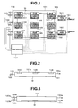
- Fig. 1 is a view showing the planar arrangement of an atomic layer film forming apparatus in the embodiment of the present invention.
- the atomic layer film forming apparatus in the embodiment includes a film forming chamber 101, gas supply pipes 121, 122, and 123, and valves 131, 132, and 133.
- a source gas or oxidizing gas e.g., ozone gas
- a gas containing a raw material for forming a thin film is supplied from one side (first side) of the film forming chamber 101 to a region in the film forming chamber 101 via the gas supply pipes 121, 122, and 123.
- the valves 131, 132, and 133 are attached to the gas supply pipes 121, 122, and 123, respectively.
- a gas supply mechanism including an evaporator for evaporating a liquid raw material is connected to the gas supply pipes 121 to 123 to be able to supply a source gas such as trimethylaluminum (TMA) gas, an oxidizing gas such as ozone gas, or a purge gas such as argon (Ar) gas.
- TMA trimethylaluminum
- Ar argon
- the atomic layer film forming apparatus includes film forming chamber monitors (film forming chamber state measurement units) 141, 142, 143, 144, 145, 146, 147, 148, and 149 which are arranged in the film forming chamber 101.
- film forming chamber monitors film forming chamber state measurement units
- the atomic layer film forming apparatus also includes exhaust pipes 151 and 152, and exhaust pipe monitors (exhaust pipe internal state measurement units) 161 and 162.
- the exhaust pipes 151 and 152 are used to evacuate the inside of the film forming chamber 101 from the other side (second side) of the film forming chamber 101.
- the exhaust pipe monitors 161 and 162 are arranged midway along the exhaust pipes 151 and 152, respectively.
- an exhaust mechanism such as a dry vacuum pump is connected to the exhaust pipes 151 and 152.
- the inside of the film forming chamber 101 can be evacuated using the dry vacuum pump and the exhaust pipes 151 and 152.
- a gas supply portion 102 formed from the gas supply pipes 121 to 123, and an exhaust portion 105 formed from the exhaust pipes 151 and 152 are arranged to face each other in the film forming chamber 101.
- the atomic layer film forming apparatus includes a controller 107 which individually controls the openings or opening times of the valves 131 to 133 based on the results of measurement by the film forming chamber monitors 141 to 149 and the exhaust pipe monitors 161 and 162.
- the film forming chamber monitors 141 to 149 are arranged on a ceiling 101a above the substrate W in the film forming chamber 101.
- the film forming chamber monitors 141, 142, and 143 are arranged on the side of the gas supply portion 102 in the film forming chamber 101.
- the film forming chamber monitors 147, 148, and 149 are arranged on the side of the exhaust portion 105 in the film forming chamber 101.
- the film forming chamber monitors 144, 145, and 146 are arranged at an intermediate position between the gas supply side and the exhaust side in the film forming chamber.
- the film forming chamber monitors 141, 144, and 147 are arrayed on the left side (left line) in the gas flow direction from the gas supply side to the exhaust side.
- the film forming chamber monitors 142, 145, and 148 are arrayed at the center (center line) in the gas flow direction from the gas supply side to the exhaust side.
- the film forming chamber monitors 143, 146, and 149 are arrayed on the right side (right line) in the gas flow direction from the gas supply side to the exhaust side.
- the film forming chamber monitors 141 to 149 can be crystal oscillation monitors (e.g., crystal oscillation film thickness monitor CRTM-9000 available from ULVAC).
- This monitor can measure the mass of a film which is deposited on a detector formed from a crystal oscillator, similarly to that deposited on the substrate W, and can measure the film thickness based on the measured mass.
- the monitor also indirectly measures the amount of gas flowing at a monitor arrangement location (on a substrate in the film forming chamber 101). Hence, the monitor functions as a film thickness measurement unit and gas amount measurement unit.
- the atomic layer film forming apparatus having the film forming chamber monitors 141 to 149, a thin film identical to one formed on the substrate W in the film forming chamber 101 is formed on the detector.
- the atomic layer film forming apparatus can, therefore, indirectly measure the thickness of the thin film formed on the substrate W.
- the film forming chamber monitors 141 to 149 indirectly measure the distribution of the thickness of the thin film formed on the substrate W. Also, the film forming chamber monitors 141 to 149 indirectly measure the distribution of the amount of gas flowing on the substrate W.
- the controller 107 individually controls the openings or opening times of the valves 131 to 133. For example, when film thicknesses measured by the film forming chamber monitors 141, 144, and 147 arrayed on the left line are larger than those measured by the film forming chamber monitors on the remaining lines, the controller 107 decreases the amount of gas supplied through the gas supply pipe 121 by decreasing the opening of the valve 131 or shortening its opening time.
- the controller 107 decreases the amount of gas supplied through the gas supply pipe 121 by decreasing the opening of the valve 131 or shortening its opening time.
- the film forming chamber monitors 141 to 149 can be ellipsometers.
- the ellipsometer can measure the film thickness and refractive index of a thin film formed on the substrate W.
- the ellipsometer functions as a film thickness measurement unit and refractive index measurement unit.
- the atomic layer film forming apparatus having the film forming chamber monitors 141 to 149 can directly measure the thickness of a thin film formed on the substrate W in the film forming chamber 101. Accordingly, the film forming chamber monitors 141 to 149 measure the distribution of the thickness of the thin film formed on the substrate W.
- the controller 107 individually controls the openings or opening times of the valves 131 to 133. For example, when film thicknesses measured by the film forming chamber monitors 141, 144, and 147 arrayed on the left line are larger than those measured by the film forming chamber monitors on the remaining lines, the controller 107 decreases the amount of gas supplied through the gas supply pipe 121 by decreasing the opening of the valve 131 or shortening its opening time.
- the film forming chamber monitors 141 to 149 can be particle monitors (foreign substance measurement units available from, e.g., HACH Ultra Analytics) which measure the state of a foreign substance (generated dust) generated in a space above the substrate W.
- the atomic layer film forming apparatus having the film forming chamber monitors 141 to 149 can measure the state of a particle (foreign substance or generated dust) generated above the substrate W in the film forming chamber 101.
- the state of generated dust is affected by the amount of gas flowing on the substrate W. For example, particles are readily generated in a region where gas is supplied more than necessary.
- the film forming chamber monitors 141 to 149 indirectly measure the distribution of gas flowing on the substrate W.
- the controller 107 individually controls the openings or opening times of the valves 131 to 133. For example, when generated dust amounts measured by the film forming chamber monitors 141, 144, and 147 arrayed on the left line are larger than those measured by the film forming chamber monitors on the remaining lines, the controller 107 decreases the amount of gas supplied through the gas supply pipe 121 by decreasing the opening of the valve 131 or shortening its opening time.
- the exhaust pipe monitor 161 measures a state in the exhaust pipe 151, whereas the exhaust pipe monitor 162 measures that in the exhaust pipe 152.
- the exhaust pipe monitors 161 and 162 can be crystal oscillation monitors. As described above, this monitor can measure the mass of a film which is deposited on a detector formed from a crystal oscillator, similarly to that deposited on the substrate W, and can measure the film thickness based on the measured mass.
- a thin film identical to one formed on the substrate W is formed on the detector from gases flowing through the exhaust pipes 151 and 152.
- the exhaust pipe monitors 161 and 162 indirectly measure the amounts of gases flowing through the exhaust pipes 151 and 152. In this manner, the exhaust pipe monitors 161 and 162 function as gas amount measurement units.
- the controller 107 individually controls the openings or opening times of the valves 131 to 133. For example, when a gas amount measured by the exhaust pipe monitor 161 is larger than that measured by the exhaust pipe monitor 162, the controller 107 decreases the amount of gas supplied through the gas supply pipe 121 by decreasing the opening of the valve 131 or shortening its opening time.
- the film forming chamber monitors 141 to 149 measure a state on the substrate W in the film forming chamber 101. Based on the measurement results, the controller 107 individually controls the openings or opening times of the valves 131 to 133. For example, if a distribution in which a film is formed thick on the left side in the widthwise direction with respect to a direction in which a supplied gas flows is confirmed from the measurement results of the film forming chamber monitors 141 to 149, the controller 107 decreases the opening of the valve 131 or shortens its opening time to decrease the gas flow rate on the left side.
- the controller 107 increases the opening of the valve 133 or prolongs its opening time to increase the gas flow rate on the right side.
- the atomic layer film forming apparatus copes with the distribution of the flow rate of gas in the film forming chamber 101 or that of the thickness of a film formed on the substrate W, which is measured by the film forming chamber monitors 141 to 149, canceling nonuniformity of the distribution.
- the three gas supply pipes 121, 122, and 123 are arranged on one side (first side) of the film forming chamber 101.
- the present invention is not limited to this, and two gas supply pipes may be arranged, or four or more gas supply pipes may be arranged.
- three film forming chamber monitors are arranged on each of the left, center, and right lines.
- one film forming chamber monitor may be arranged on each line.
- two film forming chamber monitors may be arranged at two, right and left portions. It is also possible to set four or more lines parallel in a direction in which gas flows, and arrange or array film forming chamber monitors on each line.
- a plurality of gas supply pipes such as gas supply pipes 122a and 122b may be arranged in the vertical direction of the film forming chamber 101 at the gas supply portion on one side (first side) of the film forming chamber 101. It suffices to supply, for example, an oxidizing gas through the gas supply pipe 122a and a source gas through the gas supply pipe 122b. Note that valves 132a and 132b are attached to the gas supply pipes 122a and 122b, respectively.
- a plurality of exhaust pipes such as exhaust pipes 152a and 152b may be arranged in the vertical direction of the film forming chamber 101 at the exhaust portion on the other side (second side) of the film forming chamber 101. It suffices to exhaust, for example, an oxidizing gas through the exhaust pipe 152a and a source gas through the exhaust pipe 152b.
- the controller 107 individually controls the openings or opening times of the valves 131 to 133 based on the results of measurement by the film forming chamber monitors 141 to 149 and the exhaust pipe monitors 161 and 162.
- the controller 107 may control both the openings and opening times of the valves 131 to 133.
- the controller 107 may control the openings or opening times of the valves 131 to 133 based on the results of measurement by the film forming chamber monitors 141 to 149 or the exhaust pipe monitors 161 and 162.
Landscapes
- Chemical & Material Sciences (AREA)
- General Chemical & Material Sciences (AREA)
- Chemical Kinetics & Catalysis (AREA)
- Engineering & Computer Science (AREA)
- Materials Engineering (AREA)
- Mechanical Engineering (AREA)
- Metallurgy (AREA)
- Organic Chemistry (AREA)
- Chemical Vapour Deposition (AREA)
Abstract
Description
- The present invention relates to an atomic layer film forming apparatus capable of forming a thin film for each of atomic and molecular layers.
- Recently, ALD (Atomic Layer Deposition) capable of forming a thin film for each of atomic and molecular layers is receiving attention as a technique having various features including one capable of forming a high-quality thin film more uniformly at a temperature as low as about 300°C or less. The ALD method is a technique of forming a thin film for each atomic layer by alternately supplying, to a substrate, raw materials of respective elements which constitute a film to be formed. In the ALD method, the surface adsorbs only one or n (n is an integer of 2 or more) layers while supplying raw materials of respective elements so that no unwanted raw material contributes to the growth. This is called a growth self-limiting function. The ALD method has both very excellent shape adaptability and film thickness controllability, compared to general CVD. Applications of the ALD method to the manufacture of large-screen flat panel displays are being examined as a technique capable of forming a uniform thin film in a wider area at lower temperature with good reproducibility.
- As an ALD apparatus which copes with large screens, there is proposed a lateral apparatus which supplies gas parallel to a substrate because the ALD apparatus targets a rectangular substrate more than several ten cm on a side. As is well known, the lateral apparatus supplies gas parallel to a substrate, and thus has a simple arrangement and can be easily applied to large-size substrates. As described above, the ALD method has the growth self-limiting function, and the state of a formed film is not so affected by the distribution of supplied gas in comparison with other chemical vapor deposition methods. Hence, even if the distance from the gas supply port greatly changes along with the increase in substrate size, the ALD method can be expected to form a uniform film on the entire substrate.
- The present inventors have confirmed that even when the lateral thin film forming apparatus executes atomic layer deposition, for example, the film state distribution appears between the center region of the substrate where gas flows, and a region at the end of the substrate that is spaced apart from the center region. This distribution stands out much more as the substrate size increases. To solve this, Japanese Patent Laid-Open No.
2007-157885 - However, the present inventors have also found out that no uniformity is sometimes ensured even if a plurality of gas supply ports are used to supply (spray) gas uniformly from them. In this way, the conventional technique cannot always ensure uniformity even using a plurality of gas supply ports.
- The present invention has been made to solve the above problems and has as its object to improve gas uniformity when a plurality of gas supply ports are used.
- An atomic layer film forming apparatus according to the present invention comprises a film forming chamber in which a substrate subjected to film formation is arranged, a plurality of gas supply pipes which supply, from a first side of the film forming chamber to the film forming chamber, a gas containing a raw material for forming a thin film on the substrate, a plurality of valves which are attached to the plurality of gas supply pipes, an exhaust portion which evacuates an inside of the film forming chamber from a second side of the film forming chamber that faces the first side, a film forming chamber state measurement unit which is arranged in the film forming chamber and measures a state on the substrate in the film forming chamber, and a controller which individually controls at least one of openings and opening times of the plurality of valves based on a result of measurement by the film forming chamber state measurement unit.
- According to the present invention, at least either the opening or opening time of each valve is individually controlled based on the result of measuring a state on a substrate in the film forming chamber. The present invention can therefore improve gas uniformity when a plurality of gas supply ports are used.
-
-
Fig. 1 is a view showing the planar arrangement of an atomic layer film forming apparatus in an embodiment of the present invention; -
Fig. 2 is a view showing the sectional arrangement of the atomic layer film forming apparatus shown inFig. 1 ; and -
Fig. 3 is a view showing the sectional arrangement of an atomic layer film forming apparatus in another embodiment of the present invention. - An embodiment of the present invention will now be described with reference to the accompanying drawings.
Fig. 1 is a view showing the planar arrangement of an atomic layer film forming apparatus in the embodiment of the present invention. - The atomic layer film forming apparatus in the embodiment includes a
film forming chamber 101,gas supply pipes valves film forming chamber 101 to form a thin film on a target substrate W. A gas containing a raw material for forming a thin film is supplied from one side (first side) of thefilm forming chamber 101 to a region in thefilm forming chamber 101 via thegas supply pipes valves gas supply pipes
Although not shown, as is well known, a gas supply mechanism including an evaporator for evaporating a liquid raw material is connected to thegas supply pipes 121 to 123 to be able to supply a source gas such as trimethylaluminum (TMA) gas, an oxidizing gas such as ozone gas, or a purge gas such as argon (Ar) gas. - Further, the atomic layer film forming apparatus includes film forming chamber monitors (film forming chamber state measurement units) 141, 142, 143, 144, 145, 146, 147, 148, and 149 which are arranged in the
film forming chamber 101. - The atomic layer film forming apparatus also includes
exhaust pipes exhaust pipes film forming chamber 101 from the other side (second side) of thefilm forming chamber 101. Theexhaust pipe monitors exhaust pipes exhaust pipes film forming chamber 101 can be evacuated using the dry vacuum pump and theexhaust pipes gas supply portion 102 formed from thegas supply pipes 121 to 123, and anexhaust portion 105 formed from theexhaust pipes film forming chamber 101. - In addition, the atomic layer film forming apparatus includes a
controller 107 which individually controls the openings or opening times of thevalves 131 to 133 based on the results of measurement by the film formingchamber monitors 141 to 149 and theexhaust pipe monitors - For example, as shown in
Fig. 2 , the film formingchamber monitors 141 to 149 are arranged on a ceiling 101a above the substrate W in thefilm forming chamber 101.
The film formingchamber monitors gas supply portion 102 in thefilm forming chamber 101. The film formingchamber monitors exhaust portion 105 in thefilm forming chamber 101. The film formingchamber monitors - For example, the film forming
chamber monitors chamber monitors chamber monitors
In thefilm forming chamber 101, 3 x 3 = 9 film formingchamber monitors 141 to 149 are arranged on the ceiling, and monitor a state on the substrate W, including a thin film formed on it, in thefilm forming chamber 101. - The film forming
chamber monitors 141 to 149 can be crystal oscillation monitors (e.g., crystal oscillation film thickness monitor CRTM-9000 available from ULVAC). This monitor can measure the mass of a film which is deposited on a detector formed from a crystal oscillator, similarly to that deposited on the substrate W, and can measure the film thickness based on the measured mass. Note that the monitor also indirectly measures the amount of gas flowing at a monitor arrangement location (on a substrate in the film forming chamber 101). Hence, the monitor functions as a film thickness measurement unit and gas amount measurement unit. - In the atomic layer film forming apparatus having the film forming
chamber monitors 141 to 149, a thin film identical to one formed on the substrate W in thefilm forming chamber 101 is formed on the detector. The atomic layer film forming apparatus can, therefore, indirectly measure the thickness of the thin film formed on the substrate W. The film forming chamber monitors 141 to 149 indirectly measure the distribution of the thickness of the thin film formed on the substrate W. Also, the film formingchamber monitors 141 to 149 indirectly measure the distribution of the amount of gas flowing on the substrate W. - Based on the measurement results, the
controller 107 individually controls the openings or opening times of thevalves 131 to 133. For example, when film thicknesses measured by the film formingchamber monitors controller 107 decreases the amount of gas supplied through thegas supply pipe 121 by decreasing the opening of thevalve 131 or shortening its opening time. - For example, when gas amounts measured by the film forming
chamber monitors controller 107 decreases the amount of gas supplied through thegas supply pipe 121 by decreasing the opening of thevalve 131 or shortening its opening time. - The film forming
chamber monitors 141 to 149 can be ellipsometers. The ellipsometer can measure the film thickness and refractive index of a thin film formed on the substrate W. Thus, the ellipsometer functions as a film thickness measurement unit and refractive index measurement unit. The atomic layer film forming apparatus having the film forming chamber monitors 141 to 149 can directly measure the thickness of a thin film formed on the substrate W in thefilm forming chamber 101. Accordingly, the film forming chamber monitors 141 to 149 measure the distribution of the thickness of the thin film formed on the substrate W. - Based on the measurement results, the
controller 107 individually controls the openings or opening times of thevalves 131 to 133. For example, when film thicknesses measured by the film forming chamber monitors 141, 144, and 147 arrayed on the left line are larger than those measured by the film forming chamber monitors on the remaining lines, thecontroller 107 decreases the amount of gas supplied through thegas supply pipe 121 by decreasing the opening of thevalve 131 or shortening its opening time. - Also, the film forming chamber monitors 141 to 149 can be particle monitors (foreign substance measurement units available from, e.g., HACH Ultra Analytics) which measure the state of a foreign substance (generated dust) generated in a space above the substrate W. The atomic layer film forming apparatus having the film forming chamber monitors 141 to 149 can measure the state of a particle (foreign substance or generated dust) generated above the substrate W in the
film forming chamber 101. The state of generated dust is affected by the amount of gas flowing on the substrate W. For example, particles are readily generated in a region where gas is supplied more than necessary. Hence, the film forming chamber monitors 141 to 149 indirectly measure the distribution of gas flowing on the substrate W. - Based on the measurement results, the
controller 107 individually controls the openings or opening times of thevalves 131 to 133. For example, when generated dust amounts measured by the film forming chamber monitors 141, 144, and 147 arrayed on the left line are larger than those measured by the film forming chamber monitors on the remaining lines, thecontroller 107 decreases the amount of gas supplied through thegas supply pipe 121 by decreasing the opening of thevalve 131 or shortening its opening time. - The exhaust pipe monitor 161 measures a state in the
exhaust pipe 151, whereas the exhaust pipe monitor 162 measures that in theexhaust pipe 152. - The exhaust pipe monitors 161 and 162 can be crystal oscillation monitors. As described above, this monitor can measure the mass of a film which is deposited on a detector formed from a crystal oscillator, similarly to that deposited on the substrate W, and can measure the film thickness based on the measured mass. In the atomic layer film forming apparatus having the exhaust pipe monitors 161 and 162, a thin film identical to one formed on the substrate W is formed on the detector from gases flowing through the
exhaust pipes exhaust pipes - Based on the measurement results, the
controller 107 individually controls the openings or opening times of thevalves 131 to 133. For example, when a gas amount measured by theexhaust pipe monitor 161 is larger than that measured by theexhaust pipe monitor 162, thecontroller 107 decreases the amount of gas supplied through thegas supply pipe 121 by decreasing the opening of thevalve 131 or shortening its opening time. - As described above, in the atomic layer film forming apparatus according to the embodiment, the film forming chamber monitors 141 to 149 measure a state on the substrate W in the
film forming chamber 101. Based on the measurement results, thecontroller 107 individually controls the openings or opening times of thevalves 131 to 133. For example, if a distribution in which a film is formed thick on the left side in the widthwise direction with respect to a direction in which a supplied gas flows is confirmed from the measurement results of the film forming chamber monitors 141 to 149, thecontroller 107 decreases the opening of thevalve 131 or shortens its opening time to decrease the gas flow rate on the left side. Also, thecontroller 107 increases the opening of thevalve 133 or prolongs its opening time to increase the gas flow rate on the right side. As a result, the atomic layer film forming apparatus copes with the distribution of the flow rate of gas in thefilm forming chamber 101 or that of the thickness of a film formed on the substrate W, which is measured by the film forming chamber monitors 141 to 149, canceling nonuniformity of the distribution. - In the above description, the three
gas supply pipes film forming chamber 101. However, the present invention is not limited to this, and two gas supply pipes may be arranged, or four or more gas supply pipes may be arranged.
In the above description, three film forming chamber monitors are arranged on each of the left, center, and right lines. However, the present invention is not limited to this, and for example, one film forming chamber monitor may be arranged on each line. Alternatively, two film forming chamber monitors may be arranged at two, right and left portions. It is also possible to set four or more lines parallel in a direction in which gas flows, and arrange or array film forming chamber monitors on each line. - As shown in
Fig. 3 , a plurality of gas supply pipes such as gas supply pipes 122a and 122b may be arranged in the vertical direction of thefilm forming chamber 101 at the gas supply portion on one side (first side) of thefilm forming chamber 101. It suffices to supply, for example, an oxidizing gas through the gas supply pipe 122a and a source gas through the gas supply pipe 122b. Note thatvalves
Similarly, a plurality of exhaust pipes such asexhaust pipes film forming chamber 101 at the exhaust portion on the other side (second side) of thefilm forming chamber 101. It suffices to exhaust, for example, an oxidizing gas through theexhaust pipe 152a and a source gas through theexhaust pipe 152b. - The same effects as those described above can also be obtained by individually controlling exhaust amounts through the
exhaust pipes controller 107.
In the above description, thecontroller 107 individually controls the openings or opening times of thevalves 131 to 133 based on the results of measurement by the film forming chamber monitors 141 to 149 and the exhaust pipe monitors 161 and 162. Alternatively, thecontroller 107 may control both the openings and opening times of thevalves 131 to 133. Further, thecontroller 107 may control the openings or opening times of thevalves 131 to 133 based on the results of measurement by the film forming chamber monitors 141 to 149 or the exhaust pipe monitors 161 and 162.
Claims (4)
- An atomic layer film forming apparatus comprising:a film forming chamber in which a substrate subjected to film formation is arranged;a plurality of gas supply pipes which supply, from a first side of said film forming chamber to said film forming chamber, a gas containing a raw material for forming a thin film on the substrate;a plurality of valves which are attached to said plurality of gas supply pipes;an exhaust portion which evacuates an inside of said film forming chamber from a second side of said film forming chamber that faces the first side;a film forming chamber state measurement unit which is arranged in said film forming chamber and measures a state on the substrate in said film forming chamber; anda controller which individually controls at least one of openings and opening times of said plurality of valves based on a result of measurement by said film forming chamber state measurement unit.
- An atomic layer film forming apparatus according to claim 1, wherein
said exhaust portion includes a plurality of exhaust pipes,
the atomic layer film forming apparatus further comprises a plurality of exhaust pipe internal state measurement units which are arranged on said plurality of exhaust pipes, respectively, and measure states in said plurality of exhaust pipes, and
said controller performs control based on results of measurement by said plurality of exhaust pipe internal state measurement units, in addition to the result of measurement by said film forming chamber state measurement unit. - An atomic layer film forming apparatus according to claim 1, wherein said film forming chamber state measurement unit includes at least one of a gas amount measurement unit which measures an amount of gas flowing on the substrate in said film forming chamber, a film thickness measurement unit which measures a thickness of the thin film, a refractive index measurement unit which measures a refractive index of the thin film, and a foreign substance measurement unit which measures a state of a foreign substance generated above the substrate.
- An atomic layer film forming apparatus according to claim 1, wherein said exhaust pipe internal state measurement unit includes a gas amount measurement unit which measures an amount of gas flowing through said exhaust pipe.
Applications Claiming Priority (2)
| Application Number | Priority Date | Filing Date | Title |
|---|---|---|---|
| JP2008074544A JP4430718B2 (en) | 2008-03-21 | 2008-03-21 | Atomic layer deposition system |
| PCT/JP2009/055297 WO2009116576A1 (en) | 2008-03-21 | 2009-03-18 | Atomic layer film-forming device |
Publications (2)
| Publication Number | Publication Date |
|---|---|
| EP2267183A1 true EP2267183A1 (en) | 2010-12-29 |
| EP2267183A4 EP2267183A4 (en) | 2012-01-11 |
Family
ID=41090975
Family Applications (1)
| Application Number | Title | Priority Date | Filing Date |
|---|---|---|---|
| EP09723417A Withdrawn EP2267183A4 (en) | 2008-03-21 | 2009-03-18 | Atomic layer film-forming device |
Country Status (6)
| Country | Link |
|---|---|
| US (1) | US20110017135A1 (en) |
| EP (1) | EP2267183A4 (en) |
| JP (1) | JP4430718B2 (en) |
| KR (1) | KR20100119807A (en) |
| TW (1) | TW200951245A (en) |
| WO (1) | WO2009116576A1 (en) |
Families Citing this family (9)
| Publication number | Priority date | Publication date | Assignee | Title |
|---|---|---|---|---|
| JP6359913B2 (en) * | 2014-08-12 | 2018-07-18 | 東京エレクトロン株式会社 | Processing equipment |
| US9695512B2 (en) * | 2014-09-02 | 2017-07-04 | Kabushiki Kaisha Toshiba | Semiconductor manufacturing system and semiconductor manufacturing method |
| JP6391171B2 (en) * | 2015-09-07 | 2018-09-19 | 東芝メモリ株式会社 | Semiconductor manufacturing system and operation method thereof |
| CN105386005B (en) * | 2015-11-11 | 2017-09-29 | 南通大学 | Method for preparing bismuth aluminogallate thin films whose components cross the quasi-isotype phase boundary |
| KR102770274B1 (en) * | 2019-08-06 | 2025-02-20 | 삼성전자주식회사 | Shower head and substrate treating apparatus having the same |
| TWI755979B (en) * | 2019-12-20 | 2022-02-21 | 台灣積體電路製造股份有限公司 | Thin film deposition system and method of thin film deposition |
| US12540396B2 (en) | 2019-12-20 | 2026-02-03 | Taiwan Semiconductor Manufacturing Co., Ltd. | System and method for monitoring and performing thin film deposition |
| KR102778483B1 (en) * | 2021-05-31 | 2025-03-06 | 어플라이드 머티어리얼스, 인코포레이티드 | In-situ EPI growth rate control of decision thickness micro balancing sensors |
| US12577673B2 (en) | 2022-07-18 | 2026-03-17 | Applied Materials, Inc. | In-situ EPI growth rate control of crystal thickness using parametric resonance sensing |
Family Cites Families (18)
| Publication number | Priority date | Publication date | Assignee | Title |
|---|---|---|---|---|
| JPH0718441Y2 (en) * | 1988-04-27 | 1995-05-01 | 株式会社小松製作所 | Door opening / closing device for scrap chute |
| JPH03281780A (en) * | 1990-03-30 | 1991-12-12 | Hitachi Ltd | CVD equipment |
| JP3362552B2 (en) * | 1995-03-10 | 2003-01-07 | 東京エレクトロン株式会社 | Film processing equipment |
| US5665214A (en) * | 1995-05-03 | 1997-09-09 | Sony Corporation | Automatic film deposition control method and system |
| KR100201386B1 (en) * | 1995-10-28 | 1999-06-15 | 구본준 | Reaction gas injecting apparatus of chemical vapor deposition apparatus |
| JP3341619B2 (en) * | 1997-03-04 | 2002-11-05 | 東京エレクトロン株式会社 | Film forming equipment |
| JP3830670B2 (en) * | 1998-09-03 | 2006-10-04 | 三菱電機株式会社 | Semiconductor manufacturing equipment |
| JP2000204478A (en) * | 1998-11-11 | 2000-07-25 | Canon Inc | Substrate processing apparatus and substrate processing method |
| US7515264B2 (en) * | 1999-06-15 | 2009-04-07 | Tokyo Electron Limited | Particle-measuring system and particle-measuring method |
| JP4819267B2 (en) * | 1999-08-17 | 2011-11-24 | 東京エレクトロン株式会社 | Pulse plasma processing method and apparatus |
| US6730367B2 (en) * | 2002-03-05 | 2004-05-04 | Micron Technology, Inc. | Atomic layer deposition method with point of use generated reactive gas species |
| US7153362B2 (en) * | 2002-04-30 | 2006-12-26 | Samsung Electronics Co., Ltd. | System and method for real time deposition process control based on resulting product detection |
| JP2004292852A (en) * | 2003-03-25 | 2004-10-21 | Denso Corp | Thin film forming apparatus and method |
| US20040261703A1 (en) * | 2003-06-27 | 2004-12-30 | Jeffrey D. Chinn | Apparatus and method for controlled application of reactive vapors to produce thin films and coatings |
| JP2005048208A (en) * | 2003-07-30 | 2005-02-24 | Hitachi Kokusai Electric Inc | Substrate processing equipment |
| TWI261313B (en) * | 2005-07-29 | 2006-09-01 | Ind Tech Res Inst | A method for a large dimension plasma enhanced atomic layer deposition cavity and an apparatus thereof |
| JP2007157885A (en) | 2005-12-02 | 2007-06-21 | Mitsui Eng & Shipbuild Co Ltd | Raw material gas supply device |
| KR100690177B1 (en) * | 2005-12-14 | 2007-03-08 | 동부일렉트로닉스 주식회사 | Atomic layer deposition equipment and atomic layer deposition method using the same |
-
2008
- 2008-03-21 JP JP2008074544A patent/JP4430718B2/en not_active Expired - Fee Related
-
2009
- 2009-03-18 US US12/933,677 patent/US20110017135A1/en not_active Abandoned
- 2009-03-18 WO PCT/JP2009/055297 patent/WO2009116576A1/en not_active Ceased
- 2009-03-18 KR KR1020107021219A patent/KR20100119807A/en not_active Ceased
- 2009-03-18 EP EP09723417A patent/EP2267183A4/en not_active Withdrawn
- 2009-03-20 TW TW098109130A patent/TW200951245A/en unknown
Also Published As
| Publication number | Publication date |
|---|---|
| KR20100119807A (en) | 2010-11-10 |
| US20110017135A1 (en) | 2011-01-27 |
| EP2267183A4 (en) | 2012-01-11 |
| TW200951245A (en) | 2009-12-16 |
| JP4430718B2 (en) | 2010-03-10 |
| JP2009228059A (en) | 2009-10-08 |
| WO2009116576A1 (en) | 2009-09-24 |
Similar Documents
| Publication | Publication Date | Title |
|---|---|---|
| EP2267183A1 (en) | Atomic layer film-forming device | |
| KR102718545B1 (en) | Gas distribution system and reactor system including same | |
| TWI897852B (en) | Multi-port gas injection system and reactor system including same | |
| US11208722B2 (en) | Vapor flow control apparatus for atomic layer deposition | |
| US20100092665A1 (en) | Evaporating apparatus, apparatus for controlling evaporating apparatus, method for controlling evaporating apparatus and method for using evaporating apparatus | |
| US20100326358A1 (en) | Batch type atomic layer deposition apparatus | |
| US7648578B1 (en) | Substrate processing apparatus, and method for manufacturing semiconductor device | |
| US20090304906A1 (en) | Evaporating apparatus, apparatus for controlling evaporating apparatus, method for controlling evaporating apparatus, method for using evaporating apparatus and method for manufacturing blowing port | |
| US20140209023A1 (en) | Gas supply device, processing apparatus, processing method, and storage medium | |
| US11725278B2 (en) | Systems and methods for a plasma enhanced deposition of material on a semiconductor substrate | |
| US20120328780A1 (en) | Dual Section Module Having Shared and Unshared Mass Flow Controllers | |
| CN1186873A (en) | Distribution plate for reaction chamber with multiple gas inlets and separate mass flow control loops | |
| US12614696B2 (en) | Ultra high purity conditions for atomic scale processing | |
| US20100316788A1 (en) | Deposition rate monitor device, evaporator, coating installation, method for applying vapor to a substrate and method of operating a deposition rate monitor device | |
| TWI721940B (en) | Apparatus and method for static deposition of material on a substrate | |
| TWI742632B (en) | Sputtering device | |
| TWI526568B (en) | Film forming apparatus | |
| US20160244870A1 (en) | Method for controlling a gas supply and controller | |
| JP3070728B2 (en) | Thin film vapor deposition equipment | |
| KR101573687B1 (en) | The apparatus for depositing the atomic layer | |
| KR20190096540A (en) | Atomic layer deposition system |
Legal Events
| Date | Code | Title | Description |
|---|---|---|---|
| PUAI | Public reference made under article 153(3) epc to a published international application that has entered the european phase |
Free format text: ORIGINAL CODE: 0009012 |
|
| 17P | Request for examination filed |
Effective date: 20100921 |
|
| AK | Designated contracting states |
Kind code of ref document: A1 Designated state(s): AT BE BG CH CY CZ DE DK EE ES FI FR GB GR HR HU IE IS IT LI LT LU LV MC MK MT NL NO PL PT RO SE SI SK TR |
|
| AX | Request for extension of the european patent |
Extension state: AL BA RS |
|
| DAX | Request for extension of the european patent (deleted) | ||
| A4 | Supplementary search report drawn up and despatched |
Effective date: 20111209 |
|
| RIC1 | Information provided on ipc code assigned before grant |
Ipc: C23C 16/455 20060101ALI20111205BHEP Ipc: C23C 16/52 20060101AFI20111205BHEP |
|
| STAA | Information on the status of an ep patent application or granted ep patent |
Free format text: STATUS: THE APPLICATION IS DEEMED TO BE WITHDRAWN |
|
| 18D | Application deemed to be withdrawn |
Effective date: 20120707 |