EP2265102B1 - Sensor device without housing - Google Patents
Sensor device without housing Download PDFInfo
- Publication number
- EP2265102B1 EP2265102B1 EP09014449.4A EP09014449A EP2265102B1 EP 2265102 B1 EP2265102 B1 EP 2265102B1 EP 09014449 A EP09014449 A EP 09014449A EP 2265102 B1 EP2265102 B1 EP 2265102B1
- Authority
- EP
- European Patent Office
- Prior art keywords
- circuit board
- sensor
- printed circuit
- accordance
- component parts
- Prior art date
- Legal status (The legal status is an assumption and is not a legal conclusion. Google has not performed a legal analysis and makes no representation as to the accuracy of the status listed.)
- Revoked
Links
Images

Classifications
-
- H—ELECTRICITY
- H05—ELECTRIC TECHNIQUES NOT OTHERWISE PROVIDED FOR
- H05K—PRINTED CIRCUITS; CASINGS OR CONSTRUCTIONAL DETAILS OF ELECTRIC APPARATUS; MANUFACTURE OF ASSEMBLAGES OF ELECTRICAL COMPONENTS
- H05K5/00—Casings, cabinets or drawers for electric apparatus
- H05K5/06—Hermetically-sealed casings
- H05K5/065—Hermetically-sealed casings sealed by encapsulation, e.g. waterproof resin forming an integral casing, injection moulding
-
- H—ELECTRICITY
- H05—ELECTRIC TECHNIQUES NOT OTHERWISE PROVIDED FOR
- H05K—PRINTED CIRCUITS; CASINGS OR CONSTRUCTIONAL DETAILS OF ELECTRIC APPARATUS; MANUFACTURE OF ASSEMBLAGES OF ELECTRICAL COMPONENTS
- H05K3/00—Apparatus or processes for manufacturing printed circuits
- H05K3/22—Secondary treatment of printed circuits
- H05K3/28—Applying non-metallic protective coatings
- H05K3/284—Applying non-metallic protective coatings for encapsulating mounted components
-
- H—ELECTRICITY
- H05—ELECTRIC TECHNIQUES NOT OTHERWISE PROVIDED FOR
- H05K—PRINTED CIRCUITS; CASINGS OR CONSTRUCTIONAL DETAILS OF ELECTRIC APPARATUS; MANUFACTURE OF ASSEMBLAGES OF ELECTRICAL COMPONENTS
- H05K2201/00—Indexing scheme relating to printed circuits covered by H05K1/00
- H05K2201/09—Shape and layout
- H05K2201/09818—Shape or layout details not covered by a single group of H05K2201/09009 - H05K2201/09809
- H05K2201/09872—Insulating conformal coating
-
- H—ELECTRICITY
- H05—ELECTRIC TECHNIQUES NOT OTHERWISE PROVIDED FOR
- H05K—PRINTED CIRCUITS; CASINGS OR CONSTRUCTIONAL DETAILS OF ELECTRIC APPARATUS; MANUFACTURE OF ASSEMBLAGES OF ELECTRICAL COMPONENTS
- H05K2203/00—Indexing scheme relating to apparatus or processes for manufacturing printed circuits covered by H05K3/00
- H05K2203/13—Moulding and encapsulation; Deposition techniques; Protective layers
- H05K2203/1305—Moulding and encapsulation
- H05K2203/1316—Moulded encapsulation of mounted components
Definitions
- the present invention relates to a method for the production of electronic sensors, in particular for encapsulation (in English packaging) of sensors, as well as the sensors produced by the method.
- Electronic sensors are generally used for the quantitative and / or qualitative detection of physical measured variables from their surroundings, wherein the acquired measured variables are converted and transmitted for further processing into electrical signals.
- active and passive sensors the active sensors, in addition to an actual measured value recorder, comprising additional primary electronics and being fed with an external auxiliary energy.
- inductive or capacitive proximity switches magnetic sensors, light sensors, photoelectric sensors, optical fiber sensors, inductive distance sensors, Triangulationsabstandssensoren, and phasenmesssender optical distance sensors are listed in non-exhaustive list.
- the technological structure of such sensors usually includes a robust housing which includes a Meßdorfnauf commentary and corresponding electronics on a circuit board, wherein a contacting of the sensor electronics is guided through the housing to the outside.
- a robust housing which includes a Meßdorfnauf commentary and corresponding electronics on a circuit board, wherein a contacting of the sensor electronics is guided through the housing to the outside.
- the housings are usually prefabricated of metal or plastic, so that the Meßdorfnaufsmelling, the sensor electronics and the contact, for example in the form of a cable or a plug contact can be installed in this.
- the built-in housing components of a sensor to protect against environmental influences and for mechanical stabilization of the sensor structure are poured into potting compounds.
- a respective Meß relienauf choir can consist of a single electronic, electromechanical or optoelectronic device, as well as a prefabricated group of electronic, mechanical and / or optical components.
- an angular sensor design is understood to mean a sensor having a generally polyhedral housing body, which as a rule essentially has the shape of a cuboid or several cuboids nested in one another.
- Corresponding angular sensor designs are particularly advantageous for mounting in T-slots of profile systems, which are widely used, for example, in the field of special machine construction.
- angular sensors can also be attached to any supporting elements of plants or machines.
- a disadvantage over the cylindrical sensor designs are the elaborately milled metal or plastic housing of the angular sensors whose production is relatively expensive.
- the housing can be angular Sensors are made of die-cast zinc, whereby the problem of expensive housing is shifted to high initial expenditures for the mold. In relation to small quantities, the problem of high production costs and limited flexibility in angular sensor designs remains.
- Another design is a so-called “housing-less” sensor whose electronic components are first contacted mechanically movable in the manufacturing process before they are inserted into an injection mold and held there by means of fixing in a fixed, predetermined position. The components are then completely encapsulated with a plastic compound, wherein from the plastic mass, a molded body is formed, the outer dimensions of which corresponds to the inner dimensions of the injection mold.
- a disadvantage of this method is that the individual components such as the Meßdorfnaufsmelling a sensor, a circuit board with the primary electronics and a contact individually in the injection mold must be placed consuming and precise and fixed. Furthermore, attachments must be provided on the molded body of a housing-less, angular sensor in order to assemble them at their place of use.
- the designed as threaded inserts, threaded bushings or threaded posts Fasteners must also be placed and fixed in the appropriate shape before injection molding.
- a method according to the preamble of claim 1 is disclosed in US 5,113,466 shown.
- the invention is therefore based on the object to provide a sensor that can be produced in particular in small quantities with low production costs and offers the customer an additional installation benefits.
- the present invention comprises a manufacturing method according to claim 1 for a sensor, wherein by at least partial encapsulation of a number of components with a plastic mass, a molded body, for example, is formed with angular shape whose outer dimensions correspond to the inner dimensions of an injection mold.
- a molded body for example, is formed with angular shape whose outer dimensions correspond to the inner dimensions of an injection mold.
- all optical, electronic, mechanical and / or hybrid-integrated components that are required for the function and manageability or assembly of a respective sensor can be understood as components.
- a measuring transducer designed for the respective measuring task is comprised by these components.
- the optical, electronic and / or mechanical components of the sensor are mechanically fixed on an upper side and / or rear side of a printed circuit board.
- the assembled printed circuit board inserted in the injection mold.
- the circuit board is held by means of support fingers in a defined position to the wall of the injection mold. Subsequently, the plastic mass is injected in the liquid state into the injection mold, so that the circuit board with the components in this fixed position are at least partially encapsulated.
- a transducer is preferably designed as a hybrid integrated component, which in turn comprises a number of electronic, mechanical and / or optical components corresponding to a respective measurement task, and thus forms a single prefabricated component with respect to the PCB assembly.
- the transducer is not covered by the plastic mass, or not completely embedded in the plastic mass. This may be the case, for example, in the case of optical sensors if the beam path up to the optical sensor is not to take place through the potting compound.
- the sensor is arranged in the shaft.
- the shaft element is fastened to the circuit board before encapsulation with the plastic compound, so that, viewed from above the circuit board, the shaft wall surrounds the sensor.
- the plastic mass When injecting the plastic, the plastic mass does not penetrate or at least not completely into the shaft interior, so that the shaft remains free of the plastic mass, or, so that after injection, the plastic mass through surrounds the shaft element formed shaft.
- the shaft may be sealed for sealing with a window of suitable material or an optical element.
- a sensor of an optical sensor may comprise an optoelectronic component mechanically fixed on the printed circuit board and a preassembled lens unit with a lens carrier and at least one lens.
- the lens carrier can be inserted into a groove of the printed circuit board and encapsulated in the injection mold and at least partially.
- the lens carrier preferably forms a shaft as mentioned above in the plastic mass.
- This two or more parts construction of an optical transducer allows the use of a standard optoelectronic device, e.g. a photodiode and an application-specific optics, so that it is possible to dispense with a special, prefabricated, hybrid-integrated component.
- a standard optoelectronic device e.g. a photodiode and an application-specific optics
- the lens carrier is preferably encapsulated only with its sides perpendicular to the printed circuit board, so that the outer side facing away from the optoelectronic component side of the lens carrier with the plastic molded body of the sensor can be substantially flush.
- the method according to the invention makes it possible to produce a "housing-less", for example, angular sensor, wherein a printed circuit board, which is generally required anyway for the primary electronics, is simultaneously used as a chassis, i. as an assembly platform, for the mechanical sensor structure can be shared.
- the mechanical components comprise according to the invention according to claim 1 at least one fastening element which is provided for the attachment of the sensor.
- a fastener a threaded insert or a threaded sleeve can be clipped into the circuit board, which is or completely or at least partially molded with the plastic mass by injection molding. This creates a non-positive and positive connection between the fastening element and the molded body of a sensor, whereby the forces occurring during assembly of the sensor are optimally absorbed distributed in the molded body.
- the electronic and mechanical components can be placed on the printed circuit board with a standard in electronics assembly technique, and can be fixed on the circuit board with conventional attachment methods, such as clipping, gluing and / or soldering.
- a sensor chassis can thus in a conventional pick and place machine equipped with all the components.
- circuit board benefits which includes a number of usually identical circuit boards, which are molded in the injection mold at the same time in use with the plastic compound.
- a complete or half PCB benefit as an assembly platform, a corresponding number of sensors can be provided simultaneously with an example, angular injection molded housing. The individual sensors are then separated out of the PCB benefit.
- a further embodiment of the invention provides that the assembled printed circuit board of a respective sensor are encapsulated with a transparent or semitransparent plastic compound. This allows the label of the sensor, e.g. To apply types and / or terminal designations directly on the PCB, which remains visible through the transparent body of the sensor. Thus, it is particularly advantageous to save an additional labeling imprint on the surface of the shaped body.
- the invention also includes a housing-less, for example, angular sensor according to claim 8, which could be produced by the method according to the invention.
- a sensor comprises a printed circuit board, on the upper side and / or rear side of which mechanical and electronic components are mounted, wherein the printed circuit board and the mechanical components are at least partially surrounded by a molded plastic body, wherein the molded body in Development of the invention may have, for example, a polygonal shape. All components including the Meßdorfnaufillon, which is designed as an example in an inductive proximity sensor as a coil, are thus arranged directly on the flat circuit board.
- At least one fastening element for the attachment of the sensor which may be designed as a threaded insert.
- Many sensor designs should as a rule have at least two screw connections with which a respective sensor housing is fastened to a machine or system component.
- additional dowel pins are provided on a mounting / rear side of the molded body of a sensor according to the invention, which serve for the exact positioning of the sensor, so that a second screw for mounting is dispensable.
- the dowel pins are preferably made easily removable, so that they can be broken off or cut off during assembly.
- the senor can be designed with a threaded sleeve on the back, which can also be used as a sensor attachment and for carrying out the electrical connections.
- the sensor connection is particularly advantageous in a protected machine or system part can be transferred.
- the shaped body of the sensor is made of a transparent or semitransparent Plastic running.
- a sensor lettering on the circuit board is possible and does not have to be specially applied to the surface of the molded body.
- a light-emitting diode or another display element can be arranged on the printed circuit board, which serves as a function display for the sensor.
- the display element can be fitted by machine during sensor production and can be seen at a large angle through the transparent or semitransparent shaped body of the sensor without additional components, such as light guides or transparent cover foils.
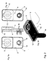
- FIG. 1 shows an inductive proximity sensor in a square sensor design with a threaded insert, which serves to attach the sensor at a designated location.
- a threaded insert could equally a threadless passage for a screw or rivet connection may be provided at this point.
- the sensor 1 comprises a printed circuit board 2, which has been equipped manually or preferably with a placement machine, wherein the components can be placed both on the top 3, and on the back 4 of the circuit board 2.
- the surfaces of the printed circuit board are provided with conventional interconnects for contacting a transducer 5, which essentially comprises a coil in the present example, the connecting cable 6 and the light-emitting diode 7, which are not explicitly shown in the present drawing.
- the printed circuit board contains additional mounting openings through which or in which the various components can be carried out or secured with a Sp Drossenietitati.
- the relevant components can additionally or alternatively be fixed by adhesive and / or solder joints on the circuit board.
- a threaded insert 8 is guided through an opening in the printed circuit board and serves to later receive a fastening screw during assembly of the sensor.
- the threaded insert can be made in one or two parts and clipped into the circuit board, riveted, glued and / or soldered.
- a strain relief (not shown in detail) for the connecting cable 6 can be integrated on the threaded insert 8.
- the connection cable 6 via a additional clamping device to be fixed to the circuit board, which is also not shown in the drawing.
- the circuit board is surrounded by a molded body 9 made of plastic, which can be produced in an injection molding process.
- the connecting cable 6 is led out through an end face of the substantially cuboid shaped body 9.
- the upper side 11 of the shaped body 9 has in the region of the high buildup coil 5 a greater distance from the circuit board in order to completely enclose the coil.
- the threaded insert 8 is flush with the surfaces on top 11 and bottom 12 of the shaped body 9 from.
- an additional dowel pin 10 is provided, which can be used for the exact positioning of the sensor during its assembly.
- the dowel pin 10 is designed so that it is easily removable by breaking off or cutting off, if this is not needed.
- the molded body 9 has on its upper side 11 and on its underside 12 recesses 13 in which the circuit board 2 has been held during injection molding of receiving finger of the injection mold.
- a light-emitting diode 7 provided on the rear side of the printed circuit board is also clearly visible from the upper side through a transparent or semitransparent shaped body of the sensor.
- a sensor shown in the figure may also comprise an electrode arrangement as a transducer 5, with which e.g. capacitive proximity sensors can be realized.
- FIG. 2 shows a further embodiment of an inductive proximity sensor shown, wherein the basic structure is substantially identical to the previously described sensor.
- the essential difference consists in the device for fastening the sensor, which is provided in the present case as a fastening sleeve 14 on the underside 12 of the shaped body 9.
- the fastening sleeve 14 is provided with two locking pins 15, which are guided through corresponding openings of the back 4 through the printed circuit board 2.
- the electrical connection of the sensor is preferably provided via the fastening sleeve 14, wherein, for example, a connection cable is guided through the interior of the fastening sleeve 14.
- a plug contact may be provided in the mounting sleeve 14.
- the electrical connections with the conductors, not shown further on the upper side 3 of the printed circuit board 2 are provided by contact legs 16, which are guided through corresponding contact holes from the back 4 through the circuit board and soldered on the top 3 with the conductor tracks.
- This embodiment is particularly advantageous for transferring the sensor connection through a housing wall into a protected machine part.
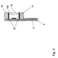
- FIG. 3 Another embodiment of the present invention is shown and shows an optical sensor.
- the sensor 1 in turn comprises a printed circuit board 2, which has been equipped with the transducer 5 and other mechanical and electronic, which have not been shown in detail repeatedly.
- To attach such a sensor come as in the FIGS. 1 and 2 shown, both the threaded inserts 8 and the mounting sleeves 14 into consideration.
- the transducer 5 comprises e.g. a photodiode 17 or other optoelectronic device soldered onto the printed circuit board 2.
- the electrical contacting of the photodiode 17 preferably takes place via the rear side 4 of the printed circuit board 2, wherein not shown in the drawing, known to the person skilled in the printed circuit board vias are used.
- the transducer additionally includes a lens unit containing a lens carrier 18 and at least one lens 19.
- the lens carrier has the shape of a tube, which is embedded in the after injection of the plastic and defines a slot 180 in the plastic mass, the inner shaft wall surrounds the transducer.
- the lens unit thus represents a prefabricated optical component that is placed above the photodiode 17 in a groove 20 on the printed circuit board 2 prior to injection molding.
- the groove 20 ensures with corresponding contact points in the injection molding tool, not shown, a mechanically sufficient fixation of the lens unit.
- a suitable contact pressure By a suitable contact pressure, a sufficient seal is ensured and thus a penetration of the plastic material between the printed circuit board 2 and lens carrier 18 is suppressed.
Description
Die vorliegende Erfindung betrifft ein Verfahren zur Fertigung von elektronischen Sensoren, insbesondere zur Kapselung (im englischen Packaging) von Sensoren, sowie die mit dem Verfahren hergestellten Sensoren.The present invention relates to a method for the production of electronic sensors, in particular for encapsulation (in English packaging) of sensors, as well as the sensors produced by the method.
Elektronische Sensoren dienen allgemein zum quantitativen und/oder qualitativen Erfassen physikalischer Messgrößen aus ihrer Umgebung, wobei die erfassten Messgrößen zur Weiterverarbeitung in elektrische Signale umgeformt und übertragen werden. Grundsätzlich kann zwischen aktiven und passiven Sensoren unterschieden werden, wobei die aktiven Sensoren neben einem eigentlichen Messgrößenaufnehmer eine zusätzliche Primärelektronik umfassen und mit einer äußeren Hilfsenergie gespeist werden. Als Beispiel für derartige elektronische Sensoren sind induktive bzw. kapazitive Näherungsschalter, Magnetsensoren, Lichttaster, Lichtschranken, Lichtwellenleitersensoren, induktive Abstandssensoren, Triangulationsabstandssensoren, und phasenmesssender optischer Abstandssensoren in nicht abschließender Aufzählung zu nennen.Electronic sensors are generally used for the quantitative and / or qualitative detection of physical measured variables from their surroundings, wherein the acquired measured variables are converted and transmitted for further processing into electrical signals. In principle, a distinction can be made between active and passive sensors, the active sensors, in addition to an actual measured value recorder, comprising additional primary electronics and being fed with an external auxiliary energy. As an example of such electronic sensors inductive or capacitive proximity switches, magnetic sensors, light sensors, photoelectric sensors, optical fiber sensors, inductive distance sensors, Triangulationsabstandssensoren, and phasenmesssender optical distance sensors are listed in non-exhaustive list.
Der technologische Aufbau solcher Sensoren umfasst in der Regel ein robustes Gehäuse, das einen Messgrößenaufnehmer und eine entsprechende Elektronik auf einer Leiterplatte beinhaltet, wobei eine Kontaktierung der Sensorelektronik durch das Gehäuse nach außen geführt ist. Als mögliche Sensorbauformen haben sich, je nach gewünschter technischer Anwendung, Sensoren sowohl mit zylindrischen als auch mit eckigen Gehäusetypen am Markt etabliert. Die Gehäuse sind in der Regel aus Metall oder Kunststoff vorgefertigt, so dass der Messgrößenaufnehmer, die Sensorelektronik sowie die Kontaktierung beispielsweise in Form eines Kabels oder eines Steckkontakts in diese eingebaut werden können. In der Regel werden die im Gehäuse eingebauten Bauelemente eines Sensors zum Schutz vor Umgebungseinflüssen und zur mechanischen Stabilisierung des Sensoraufbaus in Vergussmassen eingegossen.The technological structure of such sensors usually includes a robust housing which includes a Meßgrößenaufnehmer and corresponding electronics on a circuit board, wherein a contacting of the sensor electronics is guided through the housing to the outside. As possible sensor designs have, depending on the desired technical Application, sensors with both cylindrical and angular housing types established on the market. The housings are usually prefabricated of metal or plastic, so that the Meßgrößenaufnehmer, the sensor electronics and the contact, for example in the form of a cable or a plug contact can be installed in this. As a rule, the built-in housing components of a sensor to protect against environmental influences and for mechanical stabilization of the sensor structure are poured into potting compounds.
Ein jeweiliger Messgrößenaufnehmer kann sowohl aus einem einzelnen elektronischen, elektromechanischen oder optoelektronischen Bauelement, als auch aus einer vorgefertigten Gruppe von elektronischen, mechanischen und/oder optischen Komponenten bestehen.A respective Meßgrößenaufnehmer can consist of a single electronic, electromechanical or optoelectronic device, as well as a prefabricated group of electronic, mechanical and / or optical components.
Unter einer eckigen Sensorbauform wird im Rahmen der vorliegenden Erfindung ein Sensor mit einem im Allgemeinen polyederförmigen Gehäusekörper verstanden, der in der Regel im Wesentlichen die Form eines Quaders oder mehrerer ineinander verschachtelter Quader aufweist. Entsprechende eckige Sensorbauformen eignen sich besonders Vorteilhaft für die Montage in T-Nuten von Profilsystemen, die beispielsweise im Bereich des Sondermaschinenbaus weit verbreitet sind. Grundsätzlich können eckige Sensoren auch an beliebigen tragenden Elementen von Anlagen bzw. Maschinen befestigt werden.In the context of the present invention, an angular sensor design is understood to mean a sensor having a generally polyhedral housing body, which as a rule essentially has the shape of a cuboid or several cuboids nested in one another. Corresponding angular sensor designs are particularly advantageous for mounting in T-slots of profile systems, which are widely used, for example, in the field of special machine construction. In principle, angular sensors can also be attached to any supporting elements of plants or machines.
Nachteilig gegenüber den zylindrischen Sensorbauformen sind die aufwendig gefrästen Metall- oder Kunststoffgehäuse der eckigen Sensoren, deren Herstellung vergleichsweise kostenaufwendig ist. Alternativ können die Gehäuse eckiger Sensoren aus Zinkdruckguss hergestellt werden, wobei das Problem der teuren Gehäuse auf hohe Initialaufwendungen für die Gussform verlagert wird. Bezogen auf kleine Stückzahlen bleibt das Problem hoher Herstellkosten und eingeschränkter Flexibilität bei eckigen Sensorbauformen bestehen.A disadvantage over the cylindrical sensor designs are the elaborately milled metal or plastic housing of the angular sensors whose production is relatively expensive. Alternatively, the housing can be angular Sensors are made of die-cast zinc, whereby the problem of expensive housing is shifted to high initial expenditures for the mold. In relation to small quantities, the problem of high production costs and limited flexibility in angular sensor designs remains.
Ein weiterer Nachteil einer eckiger Sensorbauform ist, dass diese Sensoren an einer ebenen Fläche eines Maschinen- oder Anlagengehäuses mit wenigstens zwei Befestigungsschrauben montiert werden müssen, was ein gegenüber zylindrischen Sensoren einen erhöhten Aufwand darstellt.Another disadvantage of a rectangular sensor design is that these sensors must be mounted on a flat surface of a machine or plant housing with at least two mounting screws, which is an increased expense compared to cylindrical sensors.
Eine weitere Bauform stellt ein sogenannter "gehäuseloser" Sensor dar, dessen elektronische Bauelemente im Fertigungsprozess zunächst mechanisch zueinander bewegbar kontaktiert werden, bevor sie in eine Spritzgussform eingelegt und dort mittels Fixierelemente in einer festen, vorbestimmten Lage gehalten werden. Die Bauelemente werden anschließend mit einer Kunststoffmasse vollständig umspritzt, wobei aus der Kunststoffmasse ein Formkörper gebildet wird, dessen Außenabmessungen den Innenabmessungen der Spritzgussform entspricht.Another design is a so-called "housing-less" sensor whose electronic components are first contacted mechanically movable in the manufacturing process before they are inserted into an injection mold and held there by means of fixing in a fixed, predetermined position. The components are then completely encapsulated with a plastic compound, wherein from the plastic mass, a molded body is formed, the outer dimensions of which corresponds to the inner dimensions of the injection mold.
Nachteilig bei diesen Verfahren ist, dass die einzelnen Bauelemente wie der Messgrößenaufnehmer eines Sensors, eine Leiterplatte mit der Primärelektronik und einer Kontaktierung einzeln in der Spritzgussform aufwendig und präzise platziert und fixiert werden müssen. Des Weiteren müssen am Formkörper eines gehäuselosen, eckigen Sensors Befestigungen vorgesehen werden, um diese an ihrem Einsatzort montieren zu können. Die als Gewindeeinsätze, Gewindedurchführungen oder Gewindepfosten ausgeführten Befestigungen müssen ebenfalls vor dem Spritzgießen in der jeweiligen Form platziert und fixiert werden.A disadvantage of this method is that the individual components such as the Meßgrößenaufnehmer a sensor, a circuit board with the primary electronics and a contact individually in the injection mold must be placed consuming and precise and fixed. Furthermore, attachments must be provided on the molded body of a housing-less, angular sensor in order to assemble them at their place of use. The designed as threaded inserts, threaded bushings or threaded posts Fasteners must also be placed and fixed in the appropriate shape before injection molding.
Ein Verfahren nach dem Oberbegriff von Anspruch 1 wird in
Der Erfindung liegt daher die Aufgabe zugrunde, einen Sensor bereitzustellen, der insbesondere in kleinen Stückzahlen mit geringen Herstellungskosten produziert werden kann und für den Kunden einen zusätzlichen Montagenutzen bietet.The invention is therefore based on the object to provide a sensor that can be produced in particular in small quantities with low production costs and offers the customer an additional installation benefits.
Die Lösung dieser Aufgabe ist durch den Gegenstand gemäß dem unabhängigen Verfahrensanspruch und dem nebengeordneten Vorrichtungsanspruch gegeben.The solution to this problem is given by the subject matter according to the independent method claim and the independent device claim.
Bevorzugte und/oder vorteilhafte Ausführungen und Weiterbildungen sind Gegenstand der jeweiligen Unteransprüche.Preferred and / or advantageous embodiments and further developments are the subject of the respective subclaims.
Die vorliegende Erfindung umfasst ein Herstellungsverfahren nach Anspruch 1 für einen Sensor, wobei durch zumindest teilweises Umspritzen von einer Anzahl von Bauelementen mit einer Kunststoffmasse ein Formkörper, beispielsweise mit eckiger Form gebildet wird, dessen Außenabmessungen den Innenabmessungen einer Spritzgussform entsprechen. Als Bauelemente können allgemein alle optischen, elektronischen, mechanischen und/oder hybridintegrierten Bauelemente verstanden werden, die für die Funktion und Handhabbarkeit bzw. Montage eines jeweiligen Sensors erforderlich sind. Insbesondere ist ein für die jeweilige Messaufgabe ausgebildeter Messwertaufnehmer von diesen Bauelementen umfasst. In einem ersten Schritt werden die optischen, elektronischen und/oder mechanischen Bauelemente des Sensors auf einer Oberseite und/oder Rückseite einer Leiterplatte mechanisch fixiert. In einem weiteren Schritt wird die bestückte Leiterplatte in die Spritzgussform eingelegt. In der Spritzgussform wird die Leiterplatte mittels Auflagefingern in einer definierten Lage zur Wandung der Spritzgussform gehalten. Anschließend wird die Kunststoffmasse im flüssigen Zustand in die Spritzgussform gespritzt, so dass die Leiterplatte mit den Bauelementen in dieser fixierten Lage wenigstens teilweise umspritzt werden.The present invention comprises a manufacturing method according to claim 1 for a sensor, wherein by at least partial encapsulation of a number of components with a plastic mass, a molded body, for example, is formed with angular shape whose outer dimensions correspond to the inner dimensions of an injection mold. In general terms, all optical, electronic, mechanical and / or hybrid-integrated components that are required for the function and manageability or assembly of a respective sensor can be understood as components. In particular, a measuring transducer designed for the respective measuring task is comprised by these components. In a first step, the optical, electronic and / or mechanical components of the sensor are mechanically fixed on an upper side and / or rear side of a printed circuit board. In a further step, the assembled printed circuit board inserted in the injection mold. In the injection mold, the circuit board is held by means of support fingers in a defined position to the wall of the injection mold. Subsequently, the plastic mass is injected in the liquid state into the injection mold, so that the circuit board with the components in this fixed position are at least partially encapsulated.
Ein Messwertaufnehmer wird bevorzugt als ein hybridintegriertes Bauelement ausgeführt, das seinerseits entsprechend einer jeweiligen Messaufgabe eine Anzahl elektronischer, mechanischer und/oder optischer Bauelemente umfasst, und bezüglich der Leiterplattenmontage somit ein einzelnes vorgefertigtes Bauelement bildet.A transducer is preferably designed as a hybrid integrated component, which in turn comprises a number of electronic, mechanical and / or optical components corresponding to a respective measurement task, and thus forms a single prefabricated component with respect to the PCB assembly.
Gegebenenfalls kann es wünschenswert sein, dass der Messwertaufnehmer nicht von der Kunststoffmasse überdeckt, beziehungsweise nicht vollständig in der Kunststoffmasse eingebettet wird. Dies kann beispielsweise bei optischen Sensoren der Fall sein, wenn der Strahlengang bis zum optischen Sensor nicht durch die Vergussmasse erfolgen soll. Hierzu ist in Weiterbildung der Erfindung vorgesehen, ein Schachtelement in die Kunststoffmasse einzubetten, welches einen Schacht in der Kunststoffmasse bildet. Der Messwertaufnehmer ist dabei im Schacht angeordnet. Das Schachtelement wird vor dem Umspritzen mit der Kunststoffmasse auf der Platine befestigt, so dass in Aufsicht auf die Platine betrachtet die Schachtwandung den Messwertaufnehmer umgibt. Beim Einspritzen des Kunststoffs dringt die Kunststoffmasse nicht oder zumindest nicht vollständig in das Schachtinnere ein, so dass der Schacht frei von der Kunststoffmasse bleibt, beziehungsweise, so dass nach dem Einspritzen die Kunststoffmasse einen durch das Schachtelement gebildeten Schacht umgibt. Dazu ist es im allgemeinen günstig, das Schachtelement dichtend auf der Platine zu befestigen, so dass ein Eindringen der Kunststoffmasse beim Umspritzen zwischen dem zur Platine weisenden Ende des Schachtelements und der Platine verhindert wird. Im Schacht können dann auch weitere Elemente angeordnet sein. Beispielsweise kann der Schacht zur Abdichtung mit einem Fenster aus geeignetem Material oder einem optischen Element verschlossen sein.Optionally, it may be desirable that the transducer is not covered by the plastic mass, or not completely embedded in the plastic mass. This may be the case, for example, in the case of optical sensors if the beam path up to the optical sensor is not to take place through the potting compound. For this purpose, it is provided in a further development of the invention to embed a shaft element in the plastic mass, which forms a shaft in the plastic mass. The sensor is arranged in the shaft. The shaft element is fastened to the circuit board before encapsulation with the plastic compound, so that, viewed from above the circuit board, the shaft wall surrounds the sensor. When injecting the plastic, the plastic mass does not penetrate or at least not completely into the shaft interior, so that the shaft remains free of the plastic mass, or, so that after injection, the plastic mass through surrounds the shaft element formed shaft. For this purpose, it is generally advantageous to fasten the shaft element in a sealing manner on the circuit board, so that penetration of the plastic compound during encapsulation between the end of the shaft element facing the circuit board and the circuit board is prevented. In the shaft then other elements can be arranged. For example, the shaft may be sealed for sealing with a window of suitable material or an optical element.
In einer anderen, ebenfalls bevorzugten Ausführungsform oder Weiterbildung der Erfindung kann ein Messwertaufnehmer eines optischen Sensors ein auf der Leiterplatte mechanisch fixiertes optoelektronisches Bauelement sowie eine vormontierte Linseneinheit mit einem Linsenträger und wenigstens eine Linse umfassen. Der Linsenträger kann in eine Nut der Leiterplatte eingelegt und in der Spritzgussform und zumindest teilweise umspritzt werden. Hier bildet der Linsenträger vorzugsweise einen wie oben erwähnten Schacht in der Kunststoffmasse.In another, likewise preferred embodiment or development of the invention, a sensor of an optical sensor may comprise an optoelectronic component mechanically fixed on the printed circuit board and a preassembled lens unit with a lens carrier and at least one lens. The lens carrier can be inserted into a groove of the printed circuit board and encapsulated in the injection mold and at least partially. Here, the lens carrier preferably forms a shaft as mentioned above in the plastic mass.
Dieser zwei bzw. mehrteilige Aufbau eines optischen Messwertaufnehmers ermöglicht die Verwendung eines optoelektronischen Standardbauelements z.B. einer Fotodiode und einer anwendungsspezifischen Optik, so dass auf ein spezielles, vorgefertigtes, hybridintegriertes Bauelement verzichtet werden kann.This two or more parts construction of an optical transducer allows the use of a standard optoelectronic device, e.g. a photodiode and an application-specific optics, so that it is possible to dispense with a special, prefabricated, hybrid-integrated component.
Durch das Anpressen des Linsenträgers während des Spritzgießens wird verhindert, dass die noch flüssige Kunststoffmasse zwischen die Leiterplatte bzw. zwischen das optoelektronische Bauelement und der Optik eindringen kann und somit den optischen Strahlengang des Messwertaufnehmers behindert. Der Linsenträger wird bevorzugt nur mit seinen senkrecht zur Leiterplatte stehenden Seiten umspritzt, so dass die äußere, dem optoelektronischen Bauelement abgewandet Seite des Linsenträgers mit dem Kunststoffformkörper des Sensors im wesentlichen bündig abschließen kann.By pressing the lens carrier during injection molding is prevented that the still liquid plastic material between the circuit board or between the optoelectronic device and the optics can penetrate and thus the optical path of the transducer with special needs. The lens carrier is preferably encapsulated only with its sides perpendicular to the printed circuit board, so that the outer side facing away from the optoelectronic component side of the lens carrier with the plastic molded body of the sensor can be substantially flush.
Im Vergleich zum Stand der Technik ermöglicht das erfindungsgemäße Verfahren einen "gehäuselosen", beispielsweise eckigen Sensor zu fertigen, wobei eine in der Regel ohnehin für die Primärelektronik notwendige Leiterplatte gleichzeitig als Chassis, d.h. als Montageplattform, für den mechanischen Sensoraufbau mitbenutzt werden kann.In comparison to the prior art, the method according to the invention makes it possible to produce a "housing-less", for example, angular sensor, wherein a printed circuit board, which is generally required anyway for the primary electronics, is simultaneously used as a chassis, i. as an assembly platform, for the mechanical sensor structure can be shared.
Die mechanischen Bauelemente umfassen erfindungsgemäß nach Anspruch 1 wenigstens ein Befestigungselement, das für die Befestigung des Sensors vorgesehen ist. Als ein solche Befestigungselement kann ein Gewindeeinsatz oder ein Gewindehülse in die Leiterplatte eingeklippt werden, der oder die vollständig oder zumindest teilweise mit der Kunststoffmasse im Spritzgussverfahren umspritzt werden. Somit entsteht eine kraft- und formschlüssige Verbindung zwischen dem Befestigungselement und dem Formkörper eines Sensors, wodurch die bei einer Montage des Sensors auftretenden Kräfte optimal im Formkörper verteilt aufgenommen werden.The mechanical components comprise according to the invention according to claim 1 at least one fastening element which is provided for the attachment of the sensor. As such a fastener, a threaded insert or a threaded sleeve can be clipped into the circuit board, which is or completely or at least partially molded with the plastic mass by injection molding. This creates a non-positive and positive connection between the fastening element and the molded body of a sensor, whereby the forces occurring during assembly of the sensor are optimally absorbed distributed in the molded body.
Besonders vorteilhaft ist, dass die elektronischen und die mechanischen Bauelemente mit einer in der Elektronik üblichen Bestückungstechnik auf der Leiterplatte platziert werden können, und mit üblichen Befestigungsverfahren, wie einklippen, kleben und/oder löten, auf der Leiterplatte fixiert werden können. Ein Sensorchassis kann somit in einem herkömmlichen Bestückungsautomat mit den allen Bauelementen bestückt werden.It is particularly advantageous that the electronic and mechanical components can be placed on the printed circuit board with a standard in electronics assembly technique, and can be fixed on the circuit board with conventional attachment methods, such as clipping, gluing and / or soldering. A sensor chassis can thus in a conventional pick and place machine equipped with all the components.
In einer besonders vorteilhaften Weiterbildung der Erfindung kann auch ein Leiterplattennutzen, der eine Anzahl in der Regel identischer Leiterplatten umfasst, die in der Spritzgussform zeitgleich im Nutzen mit der Kunststoffmasse umspritzt werden. Mit einem kompletten oder auch halben Leiterplattennutzen als Montageplattform kann eine entsprechende Anzahl von Sensoren gleichzeitig mit einem beispielsweise eckigen Spritzgussgehäuse versehen werden. Die einzelnen Sensoren werden anschließend aus dem Leiterplattennutzen herausgetrennt.In a particularly advantageous embodiment of the invention may also be a circuit board benefits, which includes a number of usually identical circuit boards, which are molded in the injection mold at the same time in use with the plastic compound. With a complete or half PCB benefit as an assembly platform, a corresponding number of sensors can be provided simultaneously with an example, angular injection molded housing. The individual sensors are then separated out of the PCB benefit.
Eine weitere Ausgestaltung der Erfindung sieht vor, das die bestückte Leiterplatte eines jeweiligen Sensors mit einer transparenten oder halbtransparenten Kunststoffmasse umspritzt werden. Dadurch wird es ermöglicht, die Beschriftung des Sensors, z.B. Typen und/oder Anschlussbezeichnungen direkt auf der Leiterplatte aufzubringen, die durch den durchsichtigen Formkörper des Sensors sichtbar bleibt. Somit kann besonders vorteilhaft ein zusätzlicher Beschriftungsaufdruck auf der Oberfläche des Formkörpers eingespart werden.A further embodiment of the invention provides that the assembled printed circuit board of a respective sensor are encapsulated with a transparent or semitransparent plastic compound. This allows the label of the sensor, e.g. To apply types and / or terminal designations directly on the PCB, which remains visible through the transparent body of the sensor. Thus, it is particularly advantageous to save an additional labeling imprint on the surface of the shaped body.
Die Erfindung umfasst ebenfalls einen gehäuselosen, beispielsweise eckigen Sensor nach Anspruch 8, der mit dem erfindungsgemäßen Verfahren herstellbar wäre. Ein solcher Sensor umfasst eine Leiterplatte, auf dessen Oberseite und/oder Rückseite mechanische und elektronische Bauelemente montiert sind, wobei Leiterplatte und die mechanischen Bauelemente von einem Formkörper aus Kunststoff zumindest teilweise umgeben sind, wobei der Formkörper in Weiterbildung der Erfindung beispielsweise eine eckige Form aufweisen kann. Alle Bauelemente inklusive dem Messgrößenaufnehmer, der z.B. bei einem induktiven Näherungssensor als Spule ausgeführt ist, sind somit direkt auf der ebenen Leiterplatte angeordnet.The invention also includes a housing-less, for example, angular sensor according to
Auf der Leiterplatte ist unter den mechanischen Bauelementen wenigstens ein Befestigungselement für die Befestigung des Sensors vorgesehen, das als Gewindeeinsatz ausgeführt sein kann.On the circuit board is provided under the mechanical components at least one fastening element for the attachment of the sensor, which may be designed as a threaded insert.
Viele Sensorbauformen, insbesondere auch eckige Formen sollen in der Regel wenigstens zwei Schraubverbindungen, mit denen ein jeweiliges Sensorgehäuse an einem Maschinen oder Anlagenteil befestigt wird, aufweisen. Bevorzugter Weise sind an einer Montage-/Rückseite des Formkörpers eines erfindungsgemäßen Sensors zusätzliche Passstifte vorgesehen, die zur exakten Positionierung des Sensors dienen, so dass eine zweite Schraubverbindung zur Montage verzichtbar ist. Somit ist Anwenderseitig nur noch eine Bohrung an einer Maschine bzw. Anlage notwendig. Die Passstifte sind bevorzugter Weise leicht entfernbar ausgeführt, so dass sie bei der Montage abgebrochen oder abgeschnitten werden können.Many sensor designs, in particular also angular shapes, should as a rule have at least two screw connections with which a respective sensor housing is fastened to a machine or system component. Preferably, additional dowel pins are provided on a mounting / rear side of the molded body of a sensor according to the invention, which serve for the exact positioning of the sensor, so that a second screw for mounting is dispensable. Thus, only one hole on a machine or system is required by the user. The dowel pins are preferably made easily removable, so that they can be broken off or cut off during assembly.
Alternativ zum Gewindeeinsatz kann der Sensor rückseitig mit einer Gewindehülse ausgeführt sein, die gleichzeitig als Sensorbefestigung und zur Durchführung der elektrischen Anschlüsse einsetzbar ist. Somit ist der Sensoranschluss besonders vorteilhaft in einen geschützten Maschinen- bzw. Anlagenteil überführbar.As an alternative to the threaded insert, the sensor can be designed with a threaded sleeve on the back, which can also be used as a sensor attachment and for carrying out the electrical connections. Thus, the sensor connection is particularly advantageous in a protected machine or system part can be transferred.
In einer bevorzugten Ausführungsform ist der Formkörper des Sensors aus einem transparenten oder halbtransparenten Kunststoff ausgeführt. Dadurch ist eine Sensorbeschriftung auf der Leiterplatte möglich und muss nicht extra auf der Oberfläche des Formkörpers aufgebracht werden. Zusätzlich kann eine Leuchtdiode oder ein anderes Anzeigeelement auf der Leiterplatte angeordnet sein, welches als Funktionsanzeige für den Sensor dient. Das Anzeigeelement ist bei der Sensorfertigung maschinell bestückbar und ohne zusätzliche Komponenten, wie Lichtleiter oder transparente Abdeckfolien in einem großen Winkel durch den transparenten bzw. halbtransparenten Formkörper des Sensors sichtbar.In a preferred embodiment, the shaped body of the sensor is made of a transparent or semitransparent Plastic running. As a result, a sensor lettering on the circuit board is possible and does not have to be specially applied to the surface of the molded body. In addition, a light-emitting diode or another display element can be arranged on the printed circuit board, which serves as a function display for the sensor. The display element can be fitted by machine during sensor production and can be seen at a large angle through the transparent or semitransparent shaped body of the sensor without additional components, such as light guides or transparent cover foils.
Diese und weitere Merkmale sowie weitere damit einhergehende Vorteile der Erfindung ergeben sich aus der nachfolgenden näheren Beschreibung bevorzugter Ausführungsbeispiele unter Bezugnahme auf die beigefügte Zeichnungen. In den Zeichnungen zeigen:
- Fig. 1:
- einen gehäuselosen, induktiven Näherungssensor, mit einem eckigen Gehäuse und einem eingegossenen Gewindeeinsatz.
- Fig. 2:
- einen gehäuselosen, induktiven Näherungssensor, mit einem eckigen Gehäuse und einer rückseitig angeordneten Gewindehülse.
- Fig. 3:
- einen gehäuselosen, optischen Näherungssensor, mit einem eckigen Gehäuse und einem optischen Messwertaufnehmer.
- Fig. 1:
- a housing-less, inductive proximity sensor, with a square housing and a cast-in threaded insert.
- Fig. 2:
- a housing-less, inductive proximity sensor, with a square housing and a threaded sleeve on the back.
- 3:
- a caseless, optical proximity sensor, with a square housing and an optical transducer.
Die
Der Sensor 1 umfasst eine Leiterplatte 2, die manuell oder in bevorzugter Weise mit einem Bestückungsautomaten bestückt worden ist, wobei die Bauelementen sowohl auf der Oberseite 3, als auch auf der Rückseite 4 der Leiterplatte 2 platziert sein können. Die Oberflächen der Leiterplatte sind mit üblichen Leiterbahnen für die Kontaktierung eines Messwertaufnehmers 5, der im vorliegenden Beispiel im Wesentlichen eine Spule umfasst, des Anschlusskabels 6 und der Leuchtdiode 7 vorgesehen, die in der vorliegenden Zeichnung nicht explizit dargestellt sind.The sensor 1 comprises a printed
Neben den üblichen Kontaktlöchern einer Leiterplatte, die zur Kontaktierung von Spule 5 und Anschlusskabels 6 verwendbar sind, enthält die Leiterplatte zusätzliche Montageöffnungen, durch die bzw. in denen die verschiedenen Bauelemente mit einer Spreiznietverbindung durchführbar bzw. zu befestigen sind. Die betreffenden Bauelemente können zusätzlich oder alternativ durch Klebe- und/oder Lötverbindungen auf der Leiterplatte befestigt werden.In addition to the usual contact holes of a printed circuit board, which can be used for contacting
Ein Gewindeeinsatz 8 ist durch eine Öffnung in der Leiterplatte geführt und dient zur späteren Aufnahme einer Befestigungsschraube bei der Montage des Sensors. Der Gewindeeinsatz kann einteilig oder zweiteilig ausgeführt sein und in die Leiterplatte eingeklippt, aufgenietet, aufgeklebt und/oder aufgelötet sein. Des Weiteren kann an dem Gewindeeinsatz 8 eine im Detail nicht dargestellte Zugentlastung für das Anschlusskabel 6 integriert sein. Gegebenenfalls kann das Anschlusskabel 6 auch über eine zusätzliche Klemmvorrichtung an der Leiterplatte fixiert sein, die in der Zeichnung ebenfalls nicht gezeigt ist.A threaded
Die Leiterplatte ist von einem Formkörper 9 aus Kunststoff umschlossen, das in einem Spritzgussverfahren herstellbar ist. Das Anschlusskabel 6 ist dabei durch eine Stirnseite aus dem im Wesentlichen quaderförmigen Formkörper 9 herausgeführt.The circuit board is surrounded by a molded
Die Oberseite 11 des Formkörpers 9 weist im Bereich der hoch aufbauenden Spule 5 einen größeren Abstand zur Leiterplatte auf, um die Spule vollständig zu umschließen. Der Gewindeeinsatz 8 schließt bündig mit den Oberflächen auf Oberseite 11 und Unterseite 12 des Formkörpers 9 ab.The
Auf der Rückseite 12 des Formkörpers 9 ist ein zusätzlicher Passstift 10 vorgesehen, der zur exakten Positionierung des Sensors bei seiner Montage verwendet werden kann. Der Passstift 10 ist derart gestaltet, dass dieser durch Abbrechen oder Abschneiden leicht entfernbar ist, sofern dieser nicht benötigt wird.On the
Der Formkörper 9 weist auf seiner Oberseite 11 sowie auf seiner Unterseite 12 Vertiefungen 13, in denen die Leiterplatte 2 während des Spritzgießens von Aufnahmefinger der Spritzgussform gehalten worden ist.The molded
Eine auf der Rückseite der Leiterplatte vorgesehene Leuchtdiode 7, ist durch einen transparenten oder halbtransparenten Formkörper des Sensors auch von der Oberseite gut sichtbar.A light-emitting
Neben der Spule für einen induktiven Näherungssensors, kann ein in der Figur dargestellter Sensor auch eine Elektrodenanordnung als Messwertaufnehmer 5 umfassen, mit dem z.B. kapazitive Näherungssensoren realisiert werden.In addition to the coil for an inductive proximity sensor, a sensor shown in the figure may also comprise an electrode arrangement as a
Die
Der wesentliche Unterschied besteht in der Vorrichtung zur Befestigung des Sensors, die in dem vorliegenden Fall als eine Befestigungshülse 14 auf der Unterseite 12 des Formkörpers 9 vorgesehen ist.The essential difference consists in the device for fastening the sensor, which is provided in the present case as a
Die Befestigungshülse 14 ist mit zwei Verriegelungszapfen 15 versehen, die durch entsprechende Öffnungen von der Rückseite 4 durch die Leiterplatte 2 geführt sind. Der elektrische Anschluss des Sensors ist bevorzugt über die Befestigungshülse 14 bereitzustellen, wobei beispielsweise ein Anschlusskabel durch das Innere der Befestigungshülse 14 geführt ist. Alternativ kann in der Befestigungshülse 14 auch ein Steckkontakt vorgesehen sein. Die elektrischen Verbindungen mit den im weiteren nicht dargestellten Leiterbahnen auf der Oberseite 3 der Leiterplatte 2 werden durch Kontaktbeine 16 bereitgestellt, die durch entsprechende Kontaktlöcher von der Rückseite 4 durch die Leiterplatte geführt und auf der Oberseite 3 mit den Leiterbahnen verlötet sind.The
Diese Ausführung ist besonders vorteilhaft, um den Sensoranschluss durch eine Gehäusewand in einen geschützten Maschinenteil zu überführen.This embodiment is particularly advantageous for transferring the sensor connection through a housing wall into a protected machine part.
In der
Der Sensor 1 umfasst wiederum eine Leiterplatte 2, die mit dem Messwertaufnehmer 5 und weiteren mechanischen und elektronischen bestückt worden ist, die im Einzelnen nicht wiederholt dargestellt worden sind. Zur Befestigung eines solchen Sensors kommen, wie in den
The sensor 1 in turn comprises a printed
Der Messwertaufnehmer 5 umfasst z.B. eine Fotodiode 17 oder ein anderes optoelektronisches Bauelement, das auf der Leiterplatte 2 aufgelötet ist. Die elektrische Kontaktierung der Fotodiode 17 erfolgt bevorzugt über die Rückseite 4 der Leiterplatte 2, wobei in der Zeichnung nicht dargestellte, für den Fachmann der Leiterplattentechnik bekannte Durchkontaktierungen verwendet werden.The
Der Messwertaufnehmer umfasst zusätzlich eine Linseneinheit, die einem Linsenträger 18 und wenigstens eine Linse 19 enthält. Der Linsenträger hat die Gestalt eines Rohres, welches nach dem Einspritzen des Kunststoffs in die eingebettet ist und einen Schacht 180 in der Kunststoffmasse definiert, dessen innenseitige Schachtwandung den Messwertaufnehmer umgibt. Die Linseneinheit stellt somit ein vorgefertigtes optisches Bauelement dar, dass vor dem Spritzgießen in einer Nut 20 auf der Leiterplatte 2, über der Fotodiode 17 platziert wird.The transducer additionally includes a lens unit containing a
Die Nut 20 gewährleistet mit entsprechenden Auflagepunkten in dem nicht dargestellten Spritzgusswerkzeug eine mechanisch ausreichende Fixierung der Linseneinheit. Durch einen geeigneten Anpressdruck wird eine hinreichende Abdichtung gewährleistet und somit ein Durchdringen der Kunststoffmasse zwischen Leiterplatte 2 und Linsenträger 18 unterdrückt.The
Claims (15)
- Process for producing at least one sensor, whereby through the at least partial extrusion coating of a number of component parts, comprising optical, electronic, mechanical and/or hybrid component parts, but at least one measuring sensor, with a plastic compound, a preferably angular molding is formed, the outside dimensions of which correspond to the inside dimensions of an injection mold, characterized in that- the component parts (5-8, 14, 17-19) are mechanically fixed to a top side (3) and/or rear side (4) of at least one printed circuit board (2) before extrusion coating takes place,- whereby the at least one printed circuit board with the component parts mounted is inserted into the injection mold,- by means of locating fingers is held there in a defined position in relation to the walls of the injection mold,- the at least one printed circuit board with the component parts is extrusion-coated in this fixed position, and- the mechanical component parts comprise at least one fixing element (8, 14) for fixing the sensor (1), said element being at least partly extrusion-coated, so that a mechanically permanent connection is established with the molding (9).
- Process in accordance with Claim 1, characterized in that the component parts are placed, pressed, clipped, bonded and/or soldered onto the printed circuit board.
- Process in accordance with one of the above Claims, characterized in that a preassembled, hybrid-integrated component part is mechanically fixed to the printed circuit board as a measuring sensor, comprising optical, electronic and/or mechanical component parts and is at least partly extrusion-coated.
- Process in accordance with one of the above Claims, in which a shaft element is mounted on the printed circuit board before extrusion coating with the plastic compound takes place, so that when the printed circuit board is viewed from above, the shaft walls surround the measuring sensor, so that after injection molding the plastic compound surrounds a shaft formed by the shaft element.
- Process in accordance with one of the above Claims, characterized in that a measuring sensor comprises an optoelectronic component part mechanically fixed to the printed circuit board as well as a preassembled lens unit with a lens holder and at least one lens, whereby the lens holder is inserted into a groove in the printed circuit board and in the injection mold and is at least partly extrusion-coated.
- Process in accordance with one of the above Claims, characterized in that the printed circuit board is combined with a number of identical printed circuit boards to form a circuit board panel, the printed circuit boards in the circuit board panel are inserted into the injection mold and are extrusion-coated, and after the injection molding the extrusion-coated printed circuit boards are removed from the circuit board panel.
- Process in accordance with one of the above Claims, characterized in that a transparent or semi-transparent plastic is used as a plastic compound.
- Sensor comprising at least one printed circuit board (2) on the top side (3) and/or rear side (4) of which at least one optical, mechanical, electronic and/or hybrid-integrated component part (5-8, 14, 17-19) is mounted, whereby the at least one printed circuit board and the component parts are at least partly surrounded by a molding (9) made of plastic and that at least one mechanical component part is embodied on the printed circuit board as a fixing element (8, 14) for fixing the sensor (1).
- Sensor in accordance with Claim 8, characterized in that the fixing element comprises a threaded insert or a threaded sleeve.
- Sensor in accordance with the above Claim, characterized in that an electrical connection is routed through the threaded sleeve.
- Sensor in accordance with one of the Claims 8 to 10, characterized in that additional locating pins are provided for in the molding for the exact positioning of the sensor.
- Sensor in accordance with one of the Claims 8 to 11, characterized in that the component parts comprise at least one measuring sensor which is embodied as an electronic, mechanical and/or hybrid-integrated component part.
- Sensor in accordance with one of the Claims 8 to 12, characterized in that a shaft element embedded in the plastic compound is provided for, forming a shaft in the plastic compound, and whereby the measuring sensor is located in this shaft.
- Sensor in accordance with one of the Claims 8 to 13, characterized in that the component parts comprise an optical measuring sensor with an optoelectronic component part and with a lens unit extending over it with a lens holder and at least one lens.
- Sensor in accordance with one of the Claims 8 to 14, characterized in that the molding consists of a transparent or semi-transparent plastic and that preferably a light-emitting diode is provided for on the printed circuit board.
Applications Claiming Priority (1)
| Application Number | Priority Date | Filing Date | Title |
|---|---|---|---|
| DE102009029939 | 2009-06-19 |
Publications (2)
| Publication Number | Publication Date |
|---|---|
| EP2265102A1 EP2265102A1 (en) | 2010-12-22 |
| EP2265102B1 true EP2265102B1 (en) | 2014-06-25 |
Family
ID=42937336
Family Applications (1)
| Application Number | Title | Priority Date | Filing Date |
|---|---|---|---|
| EP09014449.4A Revoked EP2265102B1 (en) | 2009-06-19 | 2009-11-19 | Sensor device without housing |
Country Status (2)
| Country | Link |
|---|---|
| US (1) | US20100319470A1 (en) |
| EP (1) | EP2265102B1 (en) |
Families Citing this family (7)
| Publication number | Priority date | Publication date | Assignee | Title |
|---|---|---|---|---|
| CH699977A8 (en) * | 2008-11-25 | 2010-08-31 | Baumer Innotec Ag | Device and method for arranging a housing in a predetermined position relative to a reference object |
| US9059713B2 (en) | 2012-12-13 | 2015-06-16 | Master Lock Company Llc | Capacitive touch keypad assembly |
| US9626884B2 (en) * | 2013-03-15 | 2017-04-18 | General Led, Inc. | LED light engine for signage |
| US9464780B2 (en) * | 2013-03-15 | 2016-10-11 | General Led, Inc. | LED light engine for signage |
| DE102016211637A1 (en) * | 2016-06-28 | 2017-12-28 | Robert Bosch Gmbh | Electronic unit and method for forming an electronic unit |
| DE102017104893B4 (en) * | 2017-03-08 | 2022-01-13 | Sick Ag | Optoelectronics module and method for producing an optoelectronics module |
| IT202100030095A1 (en) * | 2021-11-29 | 2023-05-29 | B T S R Int S P A | METHOD OF MANUFACTURE OF AN OPTICAL SENSOR TO DETECT CHARACTERISTICS OF A YARN FEED TO A TEXTILE MACHINE AND RELATED OPTICAL SENSOR |
Family Cites Families (13)
| Publication number | Priority date | Publication date | Assignee | Title |
|---|---|---|---|---|
| US4911519A (en) * | 1989-02-01 | 1990-03-27 | At&T Bell Laboratories | Packaging techniques for optical transmitters/receivers |
| US5123066A (en) * | 1991-04-25 | 1992-06-16 | At&T Bell Laboratories | Molded optical package utilizing leadframe technology |
| US5113466A (en) * | 1991-04-25 | 1992-05-12 | At&T Bell Laboratories | Molded optical packaging arrangement |
| US7296345B1 (en) * | 2004-11-16 | 2007-11-20 | Super Talent Electronics, Inc. | Method for manufacturing a memory device |
| US6940058B2 (en) * | 2003-02-04 | 2005-09-06 | Kingpak Technology, Inc. | Injection molded image sensor module |
| US20050281009A1 (en) * | 2004-06-17 | 2005-12-22 | Kokusan Denki Co., Ltd. | Electronic circuit unit for internal combustion engine |
| JP2006303106A (en) * | 2005-04-19 | 2006-11-02 | Denso Corp | Electronic circuit device |
| DE502005002762D1 (en) * | 2005-06-22 | 2008-03-20 | Roche Diagnostics Gmbh | Analysis system for analyzing a sample on an analytical test element |
| WO2007131374A1 (en) * | 2006-05-12 | 2007-11-22 | Baumer Electric Ag | Proximity switch and method for contacting a sensor pcb |
| DE102007012335B4 (en) * | 2007-03-14 | 2013-10-31 | Infineon Technologies Ag | Sensor component and method for producing a sensor component |
| US20080230797A1 (en) * | 2007-03-21 | 2008-09-25 | Hui-Hung Chang | LED module and manufacturing method thereof |
| DE102008017871B4 (en) * | 2008-04-09 | 2014-09-25 | Hella Kgaa Hueck & Co. | Pressure sensor module and method for its production |
| US8234034B2 (en) * | 2009-06-26 | 2012-07-31 | Autoliv Asp, Inc. | Enhanced electronic assembly |
-
2009
- 2009-11-19 EP EP09014449.4A patent/EP2265102B1/en not_active Revoked
-
2010
- 2010-06-16 US US12/816,791 patent/US20100319470A1/en not_active Abandoned
Also Published As
| Publication number | Publication date |
|---|---|
| EP2265102A1 (en) | 2010-12-22 |
| US20100319470A1 (en) | 2010-12-23 |
Similar Documents
| Publication | Publication Date | Title |
|---|---|---|
| EP2265102B1 (en) | Sensor device without housing | |
| EP1718937B1 (en) | Sensor holder, and method for the production thereof | |
| DE102011087328B4 (en) | Method for producing an overmolded sensor assembly and a sensor assembly | |
| EP2366096B1 (en) | Assembly set for an electric motor with an angle sensor | |
| EP2406648B1 (en) | Surface-mountable magnetic field sensor having a semiconductor chip and method for producing a circuit board having a magnetic field sensor | |
| DE102010002765A1 (en) | Housing base of a multi-part housing and method for mounting a housing | |
| EP0977979B1 (en) | Method for producing a sensor module, and corresponding sensor module | |
| EP2520142B2 (en) | Sensor with a housing, and method for the production thereof | |
| EP2997645B1 (en) | Contacting part for a drive module, drive module, and method for producing a contacting part | |
| DE202005013344U1 (en) | Electrical module unit for sensor, e.g. inertia sensor, has two spraying bodies formed, so that each body surrounds number of conduction cables, and pressing grids freely running between spraying bodies and embedded in spraying bodies | |
| EP1985162B1 (en) | Holder for a flexible circuit board | |
| EP3597018B1 (en) | Electronic control module and process for manufacturing an electronic module | |
| DE102006041975A1 (en) | Ultrasonic sensor and method for producing an ultrasonic sensor | |
| EP0313956A2 (en) | Optoelectric component and manufacturing method therefore | |
| EP3289840B1 (en) | Electronics module for a transmission control unit | |
| EP3256820B1 (en) | Transmission control module | |
| DE102017104893B4 (en) | Optoelectronics module and method for producing an optoelectronics module | |
| DE102008037667B4 (en) | Process for embedding and protecting electronic circuits, and electronic component produced thereafter | |
| DE102007025890B4 (en) | Control unit for a motor vehicle and arrangement of the control unit on a system interface | |
| EP3459326A1 (en) | Method for covering an electric unit, and electric component | |
| DE102012222491A1 (en) | Electronic component with a molded component housing | |
| EP3461973B1 (en) | Handle assembly with light module and method of manufacturing | |
| DE202017101319U1 (en) | Photonics module | |
| EP3459325A1 (en) | Method for covering an electric unit, and electric component | |
| DE19742470A1 (en) | Method of manufacturing an electrical equipment with a housing, e.g. a revolution rate sensor |
Legal Events
| Date | Code | Title | Description |
|---|---|---|---|
| PUAI | Public reference made under article 153(3) epc to a published international application that has entered the european phase |
Free format text: ORIGINAL CODE: 0009012 |
|
| AK | Designated contracting states |
Kind code of ref document: A1 Designated state(s): AT BE BG CH CY CZ DE DK EE ES FI FR GB GR HR HU IE IS IT LI LT LU LV MC MK MT NL NO PL PT RO SE SI SK SM TR |
|
| AX | Request for extension of the european patent |
Extension state: AL BA RS |
|
| 17P | Request for examination filed |
Effective date: 20110610 |
|
| GRAP | Despatch of communication of intention to grant a patent |
Free format text: ORIGINAL CODE: EPIDOSNIGR1 |
|
| INTG | Intention to grant announced |
Effective date: 20140131 |
|
| RIC1 | Information provided on ipc code assigned before grant |
Ipc: H05K 5/06 20060101AFI20140117BHEP Ipc: H05K 3/28 20060101ALI20140117BHEP |
|
| RIN1 | Information on inventor provided before grant (corrected) |
Inventor name: JUERGENS, ALEXANDER Inventor name: WEHRLE, WOLFGANG |
|
| GRAS | Grant fee paid |
Free format text: ORIGINAL CODE: EPIDOSNIGR3 |
|
| GRAA | (expected) grant |
Free format text: ORIGINAL CODE: 0009210 |
|
| STAA | Information on the status of an ep patent application or granted ep patent |
Free format text: STATUS: THE PATENT HAS BEEN GRANTED |
|
| AK | Designated contracting states |
Kind code of ref document: B1 Designated state(s): AT BE BG CH CY CZ DE DK EE ES FI FR GB GR HR HU IE IS IT LI LT LU LV MC MK MT NL NO PL PT RO SE SI SK SM TR |
|
| REG | Reference to a national code |
Ref country code: GB Ref legal event code: FG4D Free format text: NOT ENGLISH |
|
| REG | Reference to a national code |
Ref country code: CH Ref legal event code: EP |
|
| REG | Reference to a national code |
Ref country code: AT Ref legal event code: REF Ref document number: 675357 Country of ref document: AT Kind code of ref document: T Effective date: 20140715 |
|
| REG | Reference to a national code |
Ref country code: IE Ref legal event code: FG4D Free format text: LANGUAGE OF EP DOCUMENT: GERMAN |
|
| REG | Reference to a national code |
Ref country code: DE Ref legal event code: R096 Ref document number: 502009009562 Country of ref document: DE Effective date: 20140807 |
|
| PG25 | Lapsed in a contracting state [announced via postgrant information from national office to epo] |
Ref country code: NO Free format text: LAPSE BECAUSE OF FAILURE TO SUBMIT A TRANSLATION OF THE DESCRIPTION OR TO PAY THE FEE WITHIN THE PRESCRIBED TIME-LIMIT Effective date: 20140925 Ref country code: CY Free format text: LAPSE BECAUSE OF FAILURE TO SUBMIT A TRANSLATION OF THE DESCRIPTION OR TO PAY THE FEE WITHIN THE PRESCRIBED TIME-LIMIT Effective date: 20140625 Ref country code: LT Free format text: LAPSE BECAUSE OF FAILURE TO SUBMIT A TRANSLATION OF THE DESCRIPTION OR TO PAY THE FEE WITHIN THE PRESCRIBED TIME-LIMIT Effective date: 20140625 Ref country code: GR Free format text: LAPSE BECAUSE OF FAILURE TO SUBMIT A TRANSLATION OF THE DESCRIPTION OR TO PAY THE FEE WITHIN THE PRESCRIBED TIME-LIMIT Effective date: 20140926 Ref country code: FI Free format text: LAPSE BECAUSE OF FAILURE TO SUBMIT A TRANSLATION OF THE DESCRIPTION OR TO PAY THE FEE WITHIN THE PRESCRIBED TIME-LIMIT Effective date: 20140625 |
|
| REG | Reference to a national code |
Ref country code: NL Ref legal event code: VDEP Effective date: 20140625 |
|
| REG | Reference to a national code |
Ref country code: LT Ref legal event code: MG4D |
|
| PG25 | Lapsed in a contracting state [announced via postgrant information from national office to epo] |
Ref country code: SE Free format text: LAPSE BECAUSE OF FAILURE TO SUBMIT A TRANSLATION OF THE DESCRIPTION OR TO PAY THE FEE WITHIN THE PRESCRIBED TIME-LIMIT Effective date: 20140625 Ref country code: HR Free format text: LAPSE BECAUSE OF FAILURE TO SUBMIT A TRANSLATION OF THE DESCRIPTION OR TO PAY THE FEE WITHIN THE PRESCRIBED TIME-LIMIT Effective date: 20140625 Ref country code: LV Free format text: LAPSE BECAUSE OF FAILURE TO SUBMIT A TRANSLATION OF THE DESCRIPTION OR TO PAY THE FEE WITHIN THE PRESCRIBED TIME-LIMIT Effective date: 20140625 |
|
| PG25 | Lapsed in a contracting state [announced via postgrant information from national office to epo] |
Ref country code: SK Free format text: LAPSE BECAUSE OF FAILURE TO SUBMIT A TRANSLATION OF THE DESCRIPTION OR TO PAY THE FEE WITHIN THE PRESCRIBED TIME-LIMIT Effective date: 20140625 Ref country code: RO Free format text: LAPSE BECAUSE OF FAILURE TO SUBMIT A TRANSLATION OF THE DESCRIPTION OR TO PAY THE FEE WITHIN THE PRESCRIBED TIME-LIMIT Effective date: 20140625 Ref country code: CZ Free format text: LAPSE BECAUSE OF FAILURE TO SUBMIT A TRANSLATION OF THE DESCRIPTION OR TO PAY THE FEE WITHIN THE PRESCRIBED TIME-LIMIT Effective date: 20140625 Ref country code: PT Free format text: LAPSE BECAUSE OF FAILURE TO SUBMIT A TRANSLATION OF THE DESCRIPTION OR TO PAY THE FEE WITHIN THE PRESCRIBED TIME-LIMIT Effective date: 20141027 Ref country code: EE Free format text: LAPSE BECAUSE OF FAILURE TO SUBMIT A TRANSLATION OF THE DESCRIPTION OR TO PAY THE FEE WITHIN THE PRESCRIBED TIME-LIMIT Effective date: 20140625 Ref country code: ES Free format text: LAPSE BECAUSE OF FAILURE TO SUBMIT A TRANSLATION OF THE DESCRIPTION OR TO PAY THE FEE WITHIN THE PRESCRIBED TIME-LIMIT Effective date: 20140625 |
|
| PG25 | Lapsed in a contracting state [announced via postgrant information from national office to epo] |
Ref country code: IS Free format text: LAPSE BECAUSE OF FAILURE TO SUBMIT A TRANSLATION OF THE DESCRIPTION OR TO PAY THE FEE WITHIN THE PRESCRIBED TIME-LIMIT Effective date: 20141025 Ref country code: NL Free format text: LAPSE BECAUSE OF FAILURE TO SUBMIT A TRANSLATION OF THE DESCRIPTION OR TO PAY THE FEE WITHIN THE PRESCRIBED TIME-LIMIT Effective date: 20140625 Ref country code: PL Free format text: LAPSE BECAUSE OF FAILURE TO SUBMIT A TRANSLATION OF THE DESCRIPTION OR TO PAY THE FEE WITHIN THE PRESCRIBED TIME-LIMIT Effective date: 20140625 |
|
| REG | Reference to a national code |
Ref country code: DE Ref legal event code: R026 Ref document number: 502009009562 Country of ref document: DE |
|
| PLBI | Opposition filed |
Free format text: ORIGINAL CODE: 0009260 |
|
| PLBI | Opposition filed |
Free format text: ORIGINAL CODE: 0009260 |
|
| PLAB | Opposition data, opponent's data or that of the opponent's representative modified |
Free format text: ORIGINAL CODE: 0009299OPPO |
|
| 26 | Opposition filed |
Opponent name: SICK AG Effective date: 20150227 |
|
| 26 | Opposition filed |
Opponent name: ASM AUTOMATION SENSORIK MESSTECHNIK GMBH Effective date: 20150325 Opponent name: LEUZE ELECTRONIC GMBH + CO. KG Effective date: 20150324 |
|
| PG25 | Lapsed in a contracting state [announced via postgrant information from national office to epo] |
Ref country code: DK Free format text: LAPSE BECAUSE OF FAILURE TO SUBMIT A TRANSLATION OF THE DESCRIPTION OR TO PAY THE FEE WITHIN THE PRESCRIBED TIME-LIMIT Effective date: 20140625 |
|
| PLAX | Notice of opposition and request to file observation + time limit sent |
Free format text: ORIGINAL CODE: EPIDOSNOBS2 |
|
| R26 | Opposition filed (corrected) |
Opponent name: ASM AUTOMATION SENSORIK MESSTECHNIK GMBH Effective date: 20150325 |
|
| REG | Reference to a national code |
Ref country code: DE Ref legal event code: R026 Ref document number: 502009009562 Country of ref document: DE Effective date: 20150227 |
|
| PG25 | Lapsed in a contracting state [announced via postgrant information from national office to epo] |
Ref country code: LU Free format text: LAPSE BECAUSE OF FAILURE TO SUBMIT A TRANSLATION OF THE DESCRIPTION OR TO PAY THE FEE WITHIN THE PRESCRIBED TIME-LIMIT Effective date: 20141119 Ref country code: MC Free format text: LAPSE BECAUSE OF FAILURE TO SUBMIT A TRANSLATION OF THE DESCRIPTION OR TO PAY THE FEE WITHIN THE PRESCRIBED TIME-LIMIT Effective date: 20140625 Ref country code: BE Free format text: LAPSE BECAUSE OF NON-PAYMENT OF DUE FEES Effective date: 20141130 |
|
| PLAF | Information modified related to communication of a notice of opposition and request to file observations + time limit |
Free format text: ORIGINAL CODE: EPIDOSCOBS2 |
|
| GBPC | Gb: european patent ceased through non-payment of renewal fee |
Effective date: 20141119 |
|
| REG | Reference to a national code |
Ref country code: IE Ref legal event code: MM4A |
|
| PG25 | Lapsed in a contracting state [announced via postgrant information from national office to epo] |
Ref country code: IE Free format text: LAPSE BECAUSE OF NON-PAYMENT OF DUE FEES Effective date: 20141119 Ref country code: GB Free format text: LAPSE BECAUSE OF NON-PAYMENT OF DUE FEES Effective date: 20141119 |
|
| PLBB | Reply of patent proprietor to notice(s) of opposition received |
Free format text: ORIGINAL CODE: EPIDOSNOBS3 |
|
| REG | Reference to a national code |
Ref country code: FR Ref legal event code: PLFP Year of fee payment: 7 |
|
| PG25 | Lapsed in a contracting state [announced via postgrant information from national office to epo] |
Ref country code: SI Free format text: LAPSE BECAUSE OF FAILURE TO SUBMIT A TRANSLATION OF THE DESCRIPTION OR TO PAY THE FEE WITHIN THE PRESCRIBED TIME-LIMIT Effective date: 20140625 |
|
| REG | Reference to a national code |
Ref country code: AT Ref legal event code: MM01 Ref document number: 675357 Country of ref document: AT Kind code of ref document: T Effective date: 20141119 |
|
| PG25 | Lapsed in a contracting state [announced via postgrant information from national office to epo] |
Ref country code: AT Free format text: LAPSE BECAUSE OF NON-PAYMENT OF DUE FEES Effective date: 20141119 |
|
| PG25 | Lapsed in a contracting state [announced via postgrant information from national office to epo] |
Ref country code: SM Free format text: LAPSE BECAUSE OF FAILURE TO SUBMIT A TRANSLATION OF THE DESCRIPTION OR TO PAY THE FEE WITHIN THE PRESCRIBED TIME-LIMIT Effective date: 20140625 |
|
| PG25 | Lapsed in a contracting state [announced via postgrant information from national office to epo] |
Ref country code: BG Free format text: LAPSE BECAUSE OF FAILURE TO SUBMIT A TRANSLATION OF THE DESCRIPTION OR TO PAY THE FEE WITHIN THE PRESCRIBED TIME-LIMIT Effective date: 20140625 |
|
| RDAF | Communication despatched that patent is revoked |
Free format text: ORIGINAL CODE: EPIDOSNREV1 |
|
| PG25 | Lapsed in a contracting state [announced via postgrant information from national office to epo] |
Ref country code: HU Free format text: LAPSE BECAUSE OF FAILURE TO SUBMIT A TRANSLATION OF THE DESCRIPTION OR TO PAY THE FEE WITHIN THE PRESCRIBED TIME-LIMIT; INVALID AB INITIO Effective date: 20091119 Ref country code: TR Free format text: LAPSE BECAUSE OF FAILURE TO SUBMIT A TRANSLATION OF THE DESCRIPTION OR TO PAY THE FEE WITHIN THE PRESCRIBED TIME-LIMIT Effective date: 20140625 Ref country code: MT Free format text: LAPSE BECAUSE OF FAILURE TO SUBMIT A TRANSLATION OF THE DESCRIPTION OR TO PAY THE FEE WITHIN THE PRESCRIBED TIME-LIMIT Effective date: 20140625 |
|
| APBM | Appeal reference recorded |
Free format text: ORIGINAL CODE: EPIDOSNREFNO |
|
| APBP | Date of receipt of notice of appeal recorded |
Free format text: ORIGINAL CODE: EPIDOSNNOA2O |
|
| APAH | Appeal reference modified |
Free format text: ORIGINAL CODE: EPIDOSCREFNO |
|
| REG | Reference to a national code |
Ref country code: FR Ref legal event code: PLFP Year of fee payment: 8 |
|
| APBQ | Date of receipt of statement of grounds of appeal recorded |
Free format text: ORIGINAL CODE: EPIDOSNNOA3O |
|
| PGFP | Annual fee paid to national office [announced via postgrant information from national office to epo] |
Ref country code: CH Payment date: 20161124 Year of fee payment: 8 |
|
| REG | Reference to a national code |
Ref country code: FR Ref legal event code: PLFP Year of fee payment: 9 |
|
| PG25 | Lapsed in a contracting state [announced via postgrant information from national office to epo] |
Ref country code: MK Free format text: LAPSE BECAUSE OF FAILURE TO SUBMIT A TRANSLATION OF THE DESCRIPTION OR TO PAY THE FEE WITHIN THE PRESCRIBED TIME-LIMIT Effective date: 20140625 |
|
| PG25 | Lapsed in a contracting state [announced via postgrant information from national office to epo] |
Ref country code: CH Free format text: LAPSE BECAUSE OF NON-PAYMENT OF DUE FEES Effective date: 20171130 Ref country code: LI Free format text: LAPSE BECAUSE OF NON-PAYMENT OF DUE FEES Effective date: 20171130 |
|
| PGFP | Annual fee paid to national office [announced via postgrant information from national office to epo] |
Ref country code: FR Payment date: 20181127 Year of fee payment: 10 |
|
| PG25 | Lapsed in a contracting state [announced via postgrant information from national office to epo] |
Ref country code: FR Free format text: LAPSE BECAUSE OF NON-PAYMENT OF DUE FEES Effective date: 20191130 |
|
| PGFP | Annual fee paid to national office [announced via postgrant information from national office to epo] |
Ref country code: IT Payment date: 20201130 Year of fee payment: 12 Ref country code: DE Payment date: 20201125 Year of fee payment: 12 |
|
| APBU | Appeal procedure closed |
Free format text: ORIGINAL CODE: EPIDOSNNOA9O |
|
| REG | Reference to a national code |
Ref country code: DE Ref legal event code: R064 Ref document number: 502009009562 Country of ref document: DE Ref country code: DE Ref legal event code: R103 Ref document number: 502009009562 Country of ref document: DE |
|
| RDAG | Patent revoked |
Free format text: ORIGINAL CODE: 0009271 |
|
| STAA | Information on the status of an ep patent application or granted ep patent |
Free format text: STATUS: PATENT REVOKED |
|
| REG | Reference to a national code |
Ref country code: FI Ref legal event code: MGE |
|
| 27W | Patent revoked |
Effective date: 20210326 |
|
| REG | Reference to a national code |
Ref country code: AT Ref legal event code: MA03 Ref document number: 675357 Country of ref document: AT Kind code of ref document: T Effective date: 20210326 |