EP2264740B1 - DRAM cell with magnetic capacitor - Google Patents
DRAM cell with magnetic capacitor Download PDFInfo
- Publication number
- EP2264740B1 EP2264740B1 EP09401012.1A EP09401012A EP2264740B1 EP 2264740 B1 EP2264740 B1 EP 2264740B1 EP 09401012 A EP09401012 A EP 09401012A EP 2264740 B1 EP2264740 B1 EP 2264740B1
- Authority
- EP
- European Patent Office
- Prior art keywords
- magnetic
- magnetic layer
- layer
- capacitor
- dram cell
- Prior art date
- Legal status (The legal status is an assumption and is not a legal conclusion. Google has not performed a legal analysis and makes no representation as to the accuracy of the status listed.)
- Not-in-force
Links
- 239000003990 capacitor Substances 0.000 title claims description 73
- 239000000758 substrate Substances 0.000 claims description 15
- 239000002184 metal Substances 0.000 claims description 11
- 239000000463 material Substances 0.000 claims description 9
- 239000004065 semiconductor Substances 0.000 claims description 7
- 239000010409 thin film Substances 0.000 claims description 7
- 230000000694 effects Effects 0.000 claims description 5
- 229910045601 alloy Inorganic materials 0.000 claims description 3
- 239000000956 alloy Substances 0.000 claims description 3
- 239000010410 layer Substances 0.000 description 78
- 230000015654 memory Effects 0.000 description 16
- 230000005855 radiation Effects 0.000 description 7
- VYPSYNLAJGMNEJ-UHFFFAOYSA-N Silicium dioxide Chemical compound O=[Si]=O VYPSYNLAJGMNEJ-UHFFFAOYSA-N 0.000 description 6
- 238000004519 manufacturing process Methods 0.000 description 5
- XUIMIQQOPSSXEZ-UHFFFAOYSA-N Silicon Chemical compound [Si] XUIMIQQOPSSXEZ-UHFFFAOYSA-N 0.000 description 4
- 229910052710 silicon Inorganic materials 0.000 description 4
- 239000010703 silicon Substances 0.000 description 4
- 239000013078 crystal Substances 0.000 description 3
- 239000000377 silicon dioxide Substances 0.000 description 3
- 238000010586 diagram Methods 0.000 description 2
- 239000003989 dielectric material Substances 0.000 description 2
- 238000009792 diffusion process Methods 0.000 description 2
- 239000000696 magnetic material Substances 0.000 description 2
- 239000012811 non-conductive material Substances 0.000 description 2
- 229910021420 polycrystalline silicon Inorganic materials 0.000 description 2
- 229920005591 polysilicon Polymers 0.000 description 2
- 235000012239 silicon dioxide Nutrition 0.000 description 2
- 239000002356 single layer Substances 0.000 description 2
- 230000003746 surface roughness Effects 0.000 description 2
- 229910052681 coesite Inorganic materials 0.000 description 1
- 230000002860 competitive effect Effects 0.000 description 1
- 229910052906 cristobalite Inorganic materials 0.000 description 1
- 230000001419 dependent effect Effects 0.000 description 1
- 238000012986 modification Methods 0.000 description 1
- 230000004048 modification Effects 0.000 description 1
- 229910052682 stishovite Inorganic materials 0.000 description 1
- 229910052905 tridymite Inorganic materials 0.000 description 1
Images


Classifications
-
- H—ELECTRICITY
- H01—ELECTRIC ELEMENTS
- H01F—MAGNETS; INDUCTANCES; TRANSFORMERS; SELECTION OF MATERIALS FOR THEIR MAGNETIC PROPERTIES
- H01F10/00—Thin magnetic films, e.g. of one-domain structure
- H01F10/32—Spin-exchange-coupled multilayers, e.g. nanostructured superlattices
- H01F10/324—Exchange coupling of magnetic film pairs via a very thin non-magnetic spacer, e.g. by exchange with conduction electrons of the spacer
- H01F10/3254—Exchange coupling of magnetic film pairs via a very thin non-magnetic spacer, e.g. by exchange with conduction electrons of the spacer the spacer being semiconducting or insulating, e.g. for spin tunnel junction [STJ]
-
- B—PERFORMING OPERATIONS; TRANSPORTING
- B82—NANOTECHNOLOGY
- B82Y—SPECIFIC USES OR APPLICATIONS OF NANOSTRUCTURES; MEASUREMENT OR ANALYSIS OF NANOSTRUCTURES; MANUFACTURE OR TREATMENT OF NANOSTRUCTURES
- B82Y25/00—Nanomagnetism, e.g. magnetoimpedance, anisotropic magnetoresistance, giant magnetoresistance or tunneling magnetoresistance
-
- G—PHYSICS
- G11—INFORMATION STORAGE
- G11C—STATIC STORES
- G11C11/00—Digital stores characterised by the use of particular electric or magnetic storage elements; Storage elements therefor
- G11C11/02—Digital stores characterised by the use of particular electric or magnetic storage elements; Storage elements therefor using magnetic elements
- G11C11/16—Digital stores characterised by the use of particular electric or magnetic storage elements; Storage elements therefor using magnetic elements using elements in which the storage effect is based on magnetic spin effect
-
- H—ELECTRICITY
- H01—ELECTRIC ELEMENTS
- H01G—CAPACITORS; CAPACITORS, RECTIFIERS, DETECTORS, SWITCHING DEVICES, LIGHT-SENSITIVE OR TEMPERATURE-SENSITIVE DEVICES OF THE ELECTROLYTIC TYPE
- H01G4/00—Fixed capacitors; Processes of their manufacture
- H01G4/002—Details
- H01G4/005—Electrodes
- H01G4/008—Selection of materials
-
- H—ELECTRICITY
- H01—ELECTRIC ELEMENTS
- H01G—CAPACITORS; CAPACITORS, RECTIFIERS, DETECTORS, SWITCHING DEVICES, LIGHT-SENSITIVE OR TEMPERATURE-SENSITIVE DEVICES OF THE ELECTROLYTIC TYPE
- H01G4/00—Fixed capacitors; Processes of their manufacture
- H01G4/33—Thin- or thick-film capacitors
-
- H—ELECTRICITY
- H01—ELECTRIC ELEMENTS
- H01L—SEMICONDUCTOR DEVICES NOT COVERED BY CLASS H10
- H01L28/00—Passive two-terminal components without a potential-jump or surface barrier for integrated circuits; Details thereof; Multistep manufacturing processes therefor
- H01L28/40—Capacitors
- H01L28/60—Electrodes
-
- H—ELECTRICITY
- H10—SEMICONDUCTOR DEVICES; ELECTRIC SOLID-STATE DEVICES NOT OTHERWISE PROVIDED FOR
- H10B—ELECTRONIC MEMORY DEVICES
- H10B12/00—Dynamic random access memory [DRAM] devices
- H10B12/01—Manufacture or treatment
- H10B12/02—Manufacture or treatment for one transistor one-capacitor [1T-1C] memory cells
- H10B12/03—Making the capacitor or connections thereto
- H10B12/033—Making the capacitor or connections thereto the capacitor extending over the transistor
-
- H—ELECTRICITY
- H10—SEMICONDUCTOR DEVICES; ELECTRIC SOLID-STATE DEVICES NOT OTHERWISE PROVIDED FOR
- H10B—ELECTRONIC MEMORY DEVICES
- H10B61/00—Magnetic memory devices, e.g. magnetoresistive RAM [MRAM] devices
- H10B61/20—Magnetic memory devices, e.g. magnetoresistive RAM [MRAM] devices comprising components having three or more electrodes, e.g. transistors
- H10B61/22—Magnetic memory devices, e.g. magnetoresistive RAM [MRAM] devices comprising components having three or more electrodes, e.g. transistors of the field-effect transistor [FET] type
Definitions
- the present invention relates to a DRAM cell. More particularly, the present invention relates to a DRAM cell with a magnetic capacitor in the metal layer. We name this device as “McRAM” (Magnetic Capcitor Random Access Memory).
- McRAM Magnetic Capcitor Random Access Memory
- a Dynamic Random Access Memory (DRAM) cell including a transistor and a storage capacitor per bit has become the most important storage element in electronic system, especially in computer and communication system.
- the output voltage of a DRAM cell is proportional to the capacitance value of the storage capacitor of the DRAM cell and, therefore, the storage capacitor must have a satisfactory capacitance value to have stable operation of the cell as the applied voltage is scaled.
- the capacitor is created in the crystal silicon layer because of the need for higher valued capacitance than is typically obtained in the other layers. Also, the capacitor is typically placed adjacent to the transistor and consumes a relatively large and valuable area on the wafer to obtain the needed capacitance values. This makes a DRAM cell large and affects the size of each bit.
- the main determinant of a DRAM's cost is the density of the memory cells.
- the goal is to have small-sized memory cells, which means that more of them can be produced at once from a single silicon wafer. This can improve yield, thus reduces the cost.
- DRAM memory cells There are several types of DRAM memory cells that are already available to increase the density, and these memory cells can be divided according to the structure of the capacitor for storing electric charge for information.
- a trench-type capacitor is formed by forming a deep trench in a semiconductor substrate without increasing the surface area of the semiconductor substrate.
- the trench-type capacitor can reduce the size of a DRAM cell, but the manufacturing process is difficult and complicated.
- US 2007/0247784 A1 relates to a magnetic capacitor used in a DRAM cell.
- the magnetic capacitor includes a dielectric which is disposed between electrodes comprising a magnetic material having a magnetic moment, wherein the magnetic moment of the opposed electrodes are anti-parallel to each other.
- GB 2 453 490 A relates to a DRAM cell with a magnetic capacitor including a substrate, a transistor and a magnetic capacitor, the capacitor being formed of two magnetic layers, between which a dielectric layer is sandwiched.
- the present invention is directed to a DRAM cell that satisfies this need of increasing the density of the memory device, simplifying the manufacturing process, and reducing the refresh rate.
- the DRAM cell includes a substrate, a transistor, and a magnetic capacitor.
- the substrate is composed of semiconductor material with a main surface
- the transistor is formed at the main surface
- the magnetic capacitor is formed in a metal layer.
- the magnetic capacitor includes a first magnetic layer, a dielectric layer formed on the surface of the first magnetic layer, and a second magnetic layer formed on the surface of the dielectric layer.
- the dielectric layer is a non-conductive material and the first magnetic layer and the second magnetic layer are formed by an alloy of CoNiFe.
- Fig. 1 is a side cross-sectional view of the DRAM cell according to a preferred embodiment of this present invention.
- Fig. 1 is a cross-sectional view of the DRAM cell according to an embodiment of the present invention.
- a DRAM cell includes a substrate 100, a transistor 120, and a magnetic capacitor 140.
- McRAM Magnetic Capcitor Random Access Memory.
- the substrate 100 is composed of semiconductor material with a main surface 102.
- the transistor 120 includes a source region 124 and a drain region 126 formed at the main surface 102 of the substrate 100.
- the transistor 120 also includes a control gate 122 placed between the source region 124 and the drain region 126, and separated from the substrate 100 by a thin control dielectric 123.
- the control gate 122 is polysilicon, and the thin control dielectric 123 may be silicon dioxide.
- the capacitor 140 is a magnetic capacitor.
- the capacitor includes a first magnetic layer 142, a dielectric layer 144 formed on the surface of the first magnetic layer 142, and a second magnetic layer 146 formed on the surface of the dielectric layer 144.
- the material for forming the dielectric layer 144 is a non-conductive material. In an embodiment, the material for forming the dielectric layer 144 is SiO 2 .
- the material for forming the first magnetic layer 142 and the second magnetic layer 146 is a magnetic material viz. an alloy of CoNiFe. The distance between the first magnetic layer 142 and the second magnetic layer 146 is larger than 100 Angstrom.
- C the capacitance of the capacitor 140
- ⁇ 0 is a constant (approximately 8.85e-12)
- ⁇ k is the dielectric constant of the material between the first magnetic layer 142 and the second magnetic layer 146
- A is the surface area of the first magnetic layer 142 and the second magnetic layer 146
- r is the distance between the first magnetic layer 142 and the second magnetic layer 146.
- GMC Gate Magnetic Capacitance
- the magnetic field is provided by the first magnetic layer 142 and the second magnetic layer 146.
- the magnetic field acts as a force to prevent escaping charges from the dielectric layer 144.
- Figure 1A is a schematic diagram to depict the magnetic field to prevent escaping charges from the dielectric layer. Since the direction of dipole 141 of the first magnetic layer 142 is opposite to that of the dipole 147 of the second magnetic layer 146, the first magnetic layer 142 and the second magnetic layer 146 generate a magnetic field 148 to prevent escaping charges from the dielectric layer 144. Therefore, the magnetic field 148 provides additional force to increase electron densities between the first magnetic layer 142 and the second magnetic layer 146. Moreover, capacitor leakage and self-discharge are essentially eliminated as electrons are "trapped" in the magnetic field 148.
- C the capacitance of the capacitor 140
- ⁇ 0 is a constant (approximately 8.85e-12)
- ⁇ k ' ⁇ k ⁇ f
- f is a modified factor
- the GMC effect factor ( ⁇ 10 6 -10 12 ) due to the magnetic field 148
- A is the surface area of the first magnetic layer 142 and the second magnetic layer 146
- r is the distance between the first magnetic layer 142 and the second magnetic layer 146.
- each of the first magnetic layer 142 and the second magnetic layer 146 is made from multiple thin film deposited layers each 1 nm thick. Therefore, the magnetic field 148 is increased by increasing the thin film deposited layers forming the first magnetic layer 142 and the second magnetic layer 146. That is that the magnetic field 148 is increased by forming additional thin film deposited layer over the original first magnetic layer 142 and the second magnetic layer 146
- the capacitance of the magnetic capacitor is significantly higher the conventional capacitor.
- the capacitor 140 is formed in the metal layer above the transistor 120.
- Conventional capacitors are created in the crystal silicon layer to obtain higher valued capacitance; however, modern capacitors are capable of obtaining the needed DRAM capacitance values when they are created in the metal layer.
- the magnetic capacitor 140 is formed above the transistor 120 in the metal layer 160.
- the magnetic capacitor 140 does not need to be created directly above the transistor 120.
- the necessary wiring connections for the DRAM cell can be placed in a routing area 180, located in between the transistor 120 and the magnetic capacitor 140, to achieve greater intensity.
- the magnetic capacitor 140 can store the information just like a standard capacitor, but has low to no leakage and high valued capacitance. Because of low to no leakage, the refresh rate is reduced to allow more time for system operation. The leakage may be so low as to eliminate the refresh altogether. This allows the removal of the refresh circuitry. Additionally, with no refresh, this memory maintains its values even after the power is removed. As a result, this invention turns DRAM into non-volatile memory, and can be used to replace Flash memories. Besides, the magnetic capacitor 140 is radiation hard in environments with high levels of radiation. This is because the energy needed to upset the magnetic capacitor 140 must be much higher than most radiation specifications to upset a bit. However, the capacitance the magnetic capacitor 140 stored to maintain memory is high enough to withstand significant radiation from environments, thus the magnetic capacitor 140 is radiation hard.
- the capacitance values of modern capacitors have increased dramatically, with dielectric constants over 3000, thinner dielectrics, and surface roughness. This allows that the magnetic capacitor 140 can take up less space than the transistor 120. Note that even though the gate length of the transistor 120 is very small, the magnetic capacitor 140 has the area for the entire transistor 120, including contacts 129 and 130, the control gate 122 and a diffusion area 121.
- a DRAM cell includes a substrate 200, a transistor 220, and a magnetic capacitor 240.
- the substrate 200 is composed of semiconductor material with a main surface 202.
- the transistor 220 includes a source region 224 and a drain region 226 formed at the main surface 202 of the substrate 200.
- the transistor 220 also includes a control gate 222 placed between the source region 224 and the drain region 226, and separated from the substrate 200 by a thin control dielectric 223.
- the control gate 222 is polysilicon, and the thin control dielectric 223 may be silicon dioxide.
- Modern capacitors are capable of obtaining the needed DRAM capacitance values when they are created in the metal layer.
- the magnetic capacitor 240 can be formed above the transistor 220.
- the magnetic capacitor 240 does not need to be created directly above the transistor 220.
- the overall area of the DRAM cell can be significantly reduced.
- the capacitor 240 is built in multiple layers with the first magnetic layer 241, the third magnetic layer 243, and the fifth magnetic layer 245.
- multiple layers can be placed to provide the desired capacitance.
- this allows for scaling to smaller dimensions because the capacitor size relative to the transistor size remains about the same. As the size of the transistor gets smaller, the amount of current it can handle also gets smaller. That is when the DRAM cell requires larger amount of capacitance relative to the size of the transistor.
- the capacitor can be built with multiple layers to provide the additional capacitance. So the first magnetic layer 241, the third magnetic layer 243, and the fifth magnetic layer 245 are placed to provide the desired capacitance for the transistor 220.
- the necessary wiring connections for the DRAM cell can be placed in a routing area 280, located in between the transistor 220 and the magnetic capacitor 240, to achieve greater intensity.
- the capacitance values of modern capacitors have increased dramatically, with dielectric constants over 3000, thinner dielectrics, and surface roughness. This allows that the magnetic capacitor 240 takes up less space than the transistor 220. Note that even though the gate length of the transistor 220 is very small, the magnetic capacitor 240 has the area for the entire transistor 220, including contacts 229 and 230, the control gate 222 and a diffusion area 221.
- the capacitor in figure 2 is built with multiple layers to provide the desired capacitance when the invention scales to small dimensions or one single layer does not provide sufficient capacitance.
- the DRAM become as Non-Volatile memory likes NAND and NOR flash when the magnetic capacitor into DRAM structure.
- this invention of a small-sized DRAM cell satisfies the need of increasing the density of the DRAM cells, thus lowers the cost of fabrication.
- the small-sized DRAM cell is achieved by creating the magnetic capacitor in the metal layer, and has the capability of increasing the speed of DRAM integrated circuits and reducing the power consumed by DRAM integrated circuits. Because of the improved speed, this memory cell can be used to replace SRAM. Furthermore, the magnetic capacitor has low to no leakage, so DRAM refresh rate can be reduced or eliminated. When DRAM refresh rate is eliminated, the refresh circuitry can be removed, and the DRAM cell becomes non-volatile. Therefore, this invention can replace other standard electronic forms of memory. Besides, the magnetic capacitor is radiation hard in environments with high levels of radiation.
Landscapes
- Engineering & Computer Science (AREA)
- Power Engineering (AREA)
- Chemical & Material Sciences (AREA)
- Microelectronics & Electronic Packaging (AREA)
- Manufacturing & Machinery (AREA)
- Crystallography & Structural Chemistry (AREA)
- Computer Hardware Design (AREA)
- Nanotechnology (AREA)
- Materials Engineering (AREA)
- Semiconductor Memories (AREA)
Description
- The present invention relates to a DRAM cell. More particularly, the present invention relates to a DRAM cell with a magnetic capacitor in the metal layer. We name this device as "McRAM" (Magnetic Capcitor Random Access Memory).
- A Dynamic Random Access Memory (DRAM) cell including a transistor and a storage capacitor per bit has become the most important storage element in electronic system, especially in computer and communication system. The output voltage of a DRAM cell is proportional to the capacitance value of the storage capacitor of the DRAM cell and, therefore, the storage capacitor must have a satisfactory capacitance value to have stable operation of the cell as the applied voltage is scaled.
- Furthermore, in a conventional DRAM cell structure, the capacitor is created in the crystal silicon layer because of the need for higher valued capacitance than is typically obtained in the other layers. Also, the capacitor is typically placed adjacent to the transistor and consumes a relatively large and valuable area on the wafer to obtain the needed capacitance values. This makes a DRAM cell large and affects the size of each bit.
- However, the main determinant of a DRAM's cost is the density of the memory cells. The goal is to have small-sized memory cells, which means that more of them can be produced at once from a single silicon wafer. This can improve yield, thus reduces the cost.
- There are several types of DRAM memory cells that are already available to increase the density, and these memory cells can be divided according to the structure of the capacitor for storing electric charge for information. For example, a trench-type capacitor is formed by forming a deep trench in a semiconductor substrate without increasing the surface area of the semiconductor substrate. The trench-type capacitor can reduce the size of a DRAM cell, but the manufacturing process is difficult and complicated.
- Besides, even though these already available memory cells have high density, it comes with the cost of having to refresh the memory periodically. Additional circuitry is required to read and re-write each bit in the memory. This makes the DRAM circuit more complicated, and this means that the memory was not always available for system use because it may be in a refresh cycle. Furthermore, the additional circuitry detracts from the density. DRAM memories are not scaling to remain competitive because of the high area taken by the capacitors used to store the value of the bit.
-
US 2007/0247784 A1 relates to a magnetic capacitor used in a DRAM cell. The magnetic capacitor includes a dielectric which is disposed between electrodes comprising a magnetic material having a magnetic moment, wherein the magnetic moment of the opposed electrodes are anti-parallel to each other. -
GB 2 453 490 A - Starting from the latter state of the art it is the object of the present application to provide a new DRAM cell, so that the density of a DRAM may be increased, the manufacturing process is simplified, and the refresh rate is reduced. Thus the cost of manufacturing is reduced.
- The above-mentioned object is solved by the DRAM cell according to claim 1. Advantageous improvements of the present invention are the subject matter of dependent claims.
- The present invention is directed to a DRAM cell that satisfies this need of increasing the density of the memory device, simplifying the manufacturing process, and reducing the refresh rate.
- The DRAM cell includes a substrate, a transistor, and a magnetic capacitor. The substrate is composed of semiconductor material with a main surface, the transistor is formed at the main surface, and the magnetic capacitor is formed in a metal layer. The magnetic capacitor includes a first magnetic layer, a dielectric layer formed on the surface of the first magnetic layer, and a second magnetic layer formed on the surface of the dielectric layer.
- The dielectric layer is a non-conductive material and the first magnetic layer and the second magnetic layer are formed by an alloy of CoNiFe.
- The accompanying drawings are included to provide a further understanding of the invention, and are incorporated in and constitute a part of this specification. The drawings illustrate an embodiment of the invention and, together with the description, serve to explain the principles of the invention. In the drawings,
Fig. 1 is a side cross-sectional view of the DRAM cell according to a preferred embodiment of this present invention. -
Figure 1A is a schematic diagram to depict the magnetic field to prevent escaping charges from the dielectric layer. -
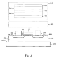
Fig. 2 is a side cross-sectional view of the DRAM cell according to an example not forming part of the claimed invention. - Reference will now be made in detail to the present preferred embodiment of the invention, an example of which is illustrated in the accompanying drawings. Wherever possible, the same reference numbers are used in the drawings and the description to refer to the same or like parts.
- Please refer to
Fig. 1. Fig. 1 is a cross-sectional view of the DRAM cell according to an embodiment of the present invention. A DRAM cell includes asubstrate 100, atransistor 120, and amagnetic capacitor 140. We name this device as "McRAM" (Magnetic Capcitor Random Access Memory. However, in the following paragraph, we still use DRAM to describe this invention. Thesubstrate 100 is composed of semiconductor material with amain surface 102. Thetransistor 120 includes asource region 124 and adrain region 126 formed at themain surface 102 of thesubstrate 100. Thetransistor 120 also includes acontrol gate 122 placed between thesource region 124 and thedrain region 126, and separated from thesubstrate 100 by a thin control dielectric 123. Thecontrol gate 122 is polysilicon, and the thin control dielectric 123 may be silicon dioxide. - The
capacitor 140 is a magnetic capacitor. The capacitor includes a firstmagnetic layer 142, adielectric layer 144 formed on the surface of the firstmagnetic layer 142, and a secondmagnetic layer 146 formed on the surface of thedielectric layer 144. The material for forming thedielectric layer 144 is a non-conductive material. In an embodiment, the material for forming thedielectric layer 144 is SiO2. The material for forming the firstmagnetic layer 142 and the secondmagnetic layer 146 is a magnetic material viz. an alloy of CoNiFe. The distance between the firstmagnetic layer 142 and the secondmagnetic layer 146 is larger than 100 Angstrom. Capacitors are generally governed by this equation (1):
capacitor 140, ε 0 is a constant (approximately 8.85e-12), ε k is the dielectric constant of the material between the firstmagnetic layer 142 and the secondmagnetic layer 146, A is the surface area of the firstmagnetic layer 142 and the secondmagnetic layer 146, and r is the distance between the firstmagnetic layer 142 and the secondmagnetic layer 146. From the equation (1), if the dielectric constant ε k of the material between the firstmagnetic layer 142 and the secondmagnetic layer 146 increases, the capacitance will increase. - A GMC (Giant Magnetic Capacitance) effect is used to increase the dielectric constant ε k . GMC acts, figuratively, like a charge trap that brings electrons to closer, thus increasing electron densities between the first
magnetic layer 142 and the secondmagnetic layer 146. - The magnetic field is provided by the first
magnetic layer 142 and the secondmagnetic layer 146. The magnetic field acts as a force to prevent escaping charges from thedielectric layer 144. -
Figure 1A is a schematic diagram to depict the magnetic field to prevent escaping charges from the dielectric layer. Since the direction ofdipole 141 of the firstmagnetic layer 142 is opposite to that of thedipole 147 of the secondmagnetic layer 146, the firstmagnetic layer 142 and the secondmagnetic layer 146 generate amagnetic field 148 to prevent escaping charges from thedielectric layer 144. Therefore, themagnetic field 148 provides additional force to increase electron densities between the firstmagnetic layer 142 and the secondmagnetic layer 146. Moreover, capacitor leakage and self-discharge are essentially eliminated as electrons are "trapped" in themagnetic field 148. - Thus, with the strong magnetic field, the capacitance is therefore governed by a modified equation:

capacitor 140,
ε 0 is a constant (approximately 8.85e-12),
ε k' = ε k × f, where f is a modified factor, the GMC effect factor (∼106-1012), due to themagnetic field 148, - A is the surface area of the first
magnetic layer 142 and the secondmagnetic layer 146,
r is the distance between the firstmagnetic layer 142 and the secondmagnetic layer 146. - In other words, when the
magnetic field 148 is increased, the capacitance is therefore increased. Each of the firstmagnetic layer 142 and the secondmagnetic layer 146 is made from multiple thin film deposited layers each 1 nm thick. Therefore, themagnetic field 148 is increased by increasing the thin film deposited layers forming the firstmagnetic layer 142 and the secondmagnetic layer 146. That is that themagnetic field 148 is increased by forming additional thin film deposited layer over the original firstmagnetic layer 142 and the secondmagnetic layer 146 - It is noted that the symbols '→' are arranged to represent the dipoles of the magnetic sections.
- The following table compares the capacitance of a magnetic capacitor with that of a conventional capacitor.
Magnetic capacitor #1 Magnetic capacitor #2 Mcap capacitance measured (Average) 1.2 nF (at 1kHz) 96 uF (at 1kHz) GMC factor (f) (Average) 2.0 x 10⁶ 1.6 x 10¹¹ Conventional capacitance* (i.e. no GMC effect) 0.6 fF (at k=3.4) 0.6 fF (at k=3.4) 
- Because of the f factor, GMC effect factor (∼106-1012), from the magnetic field generated by the first
magnetic layer 142 and the secondmagnetic layer 146, the capacitance of the magnetic capacitor is significantly higher the conventional capacitor. - Notice that the
capacitor 140 is formed in the metal layer above thetransistor 120. Conventional capacitors are created in the crystal silicon layer to obtain higher valued capacitance; however, modern capacitors are capable of obtaining the needed DRAM capacitance values when they are created in the metal layer. As a result, themagnetic capacitor 140 is formed above thetransistor 120 in the metal layer 160. However, themagnetic capacitor 140 does not need to be created directly above thetransistor 120. When themagnetic capacitor 140 is moved from the crystal silicon layer to the metal layer 160, the overall area of the DRAM cell can be significantly reduced. Besides, the necessary wiring connections for the DRAM cell can be placed in arouting area 180, located in between thetransistor 120 and themagnetic capacitor 140, to achieve greater intensity. - With the
magnetic capacitor 140 formed in the metal layer of semiconductors, it is now possible to reduce or eliminate the DRAM refresh rate. Themagnetic capacitor 140 can store the information just like a standard capacitor, but has low to no leakage and high valued capacitance. Because of low to no leakage, the refresh rate is reduced to allow more time for system operation. The leakage may be so low as to eliminate the refresh altogether. This allows the removal of the refresh circuitry. Additionally, with no refresh, this memory maintains its values even after the power is removed. As a result, this invention turns DRAM into non-volatile memory, and can be used to replace Flash memories. Besides, themagnetic capacitor 140 is radiation hard in environments with high levels of radiation. This is because the energy needed to upset themagnetic capacitor 140 must be much higher than most radiation specifications to upset a bit. However, the capacitance themagnetic capacitor 140 stored to maintain memory is high enough to withstand significant radiation from environments, thus themagnetic capacitor 140 is radiation hard. - Furthermore, the capacitance values of modern capacitors have increased dramatically, with dielectric constants over 3000, thinner dielectrics, and surface roughness. This allows that the
magnetic capacitor 140 can take up less space than thetransistor 120. Note that even though the gate length of thetransistor 120 is very small, themagnetic capacitor 140 has the area for theentire transistor 120, includingcontacts control gate 122 and adiffusion area 121. - Please refer to
Fig. 2 , a cross-sectional view of the DRAM cell according to an example not forming part of the claimed invention. A DRAM cell includes asubstrate 200, atransistor 220, and amagnetic capacitor 240. Thesubstrate 200 is composed of semiconductor material with amain surface 202. Thetransistor 220 includes asource region 224 and adrain region 226 formed at themain surface 202 of thesubstrate 200. Thetransistor 220 also includes acontrol gate 222 placed between thesource region 224 and thedrain region 226, and separated from thesubstrate 200 by athin control dielectric 223. Thecontrol gate 222 is polysilicon, and the thin control dielectric 223 may be silicon dioxide. - Modern capacitors are capable of obtaining the needed DRAM capacitance values when they are created in the metal layer. As a result, the
magnetic capacitor 240 can be formed above thetransistor 220. However, themagnetic capacitor 240 does not need to be created directly above thetransistor 220. When themagnetic capacitor 240 is created in the metal layer, the overall area of the DRAM cell can be significantly reduced. - Notice that the
capacitor 240 is built in multiple layers with the firstmagnetic layer 241, the thirdmagnetic layer 243, and the fifthmagnetic layer 245. When the capacitor does not provide sufficient capacitance with a single layer of capacitance, multiple layers can be placed to provide the desired capacitance. In addition, this allows for scaling to smaller dimensions because the capacitor size relative to the transistor size remains about the same. As the size of the transistor gets smaller, the amount of current it can handle also gets smaller. That is when the DRAM cell requires larger amount of capacitance relative to the size of the transistor. The capacitor can be built with multiple layers to provide the additional capacitance. So the firstmagnetic layer 241, the thirdmagnetic layer 243, and the fifthmagnetic layer 245 are placed to provide the desired capacitance for thetransistor 220. - Besides, the necessary wiring connections for the DRAM cell can be placed in a
routing area 280, located in between thetransistor 220 and themagnetic capacitor 240, to achieve greater intensity. Lastly, the capacitance values of modern capacitors have increased dramatically, with dielectric constants over 3000, thinner dielectrics, and surface roughness. This allows that themagnetic capacitor 240 takes up less space than thetransistor 220. Note that even though the gate length of thetransistor 220 is very small, themagnetic capacitor 240 has the area for theentire transistor 220, includingcontacts control gate 222 and adiffusion area 221. - The difference between the
figure 1 embodiment and thefigure 2 example is that the capacitor infigure 2 is built with multiple layers to provide the desired capacitance when the invention scales to small dimensions or one single layer does not provide sufficient capacitance. - Moreover, since the magnetic capacitor still can retain the electric charge when the power supplied to the magnetic capacitor is off, the DRAM become as Non-Volatile memory likes NAND and NOR flash when the magnetic capacitor into DRAM structure.
- From the description above, we can conclude that this invention of a small-sized DRAM cell satisfies the need of increasing the density of the DRAM cells, thus lowers the cost of fabrication. The small-sized DRAM cell is achieved by creating the magnetic capacitor in the metal layer, and has the capability of increasing the speed of DRAM integrated circuits and reducing the power consumed by DRAM integrated circuits. Because of the improved speed, this memory cell can be used to replace SRAM. Furthermore, the magnetic capacitor has low to no leakage, so DRAM refresh rate can be reduced or eliminated. When DRAM refresh rate is eliminated, the refresh circuitry can be removed, and the DRAM cell becomes non-volatile. Therefore, this invention can replace other standard electronic forms of memory. Besides, the magnetic capacitor is radiation hard in environments with high levels of radiation.
- It will be apparent to those skilled in the art that various modifications and variations can be made to the structure of the present invention whithin the scope of the claims.
Claims (4)
- A DRAM cell, comprising:a substrate (100) having semiconductor material with a main surface (102);a transistor (120) formed at the main surface (102); anda magnetic capacitor (140) formed in a metal layer located above the transistor (120), wherein the magnetic capacitor (140) includes:a first magnetic layer (142);a dielectric layer (144) formed on the surface of the first magnetic layer (142); anda second magnetic layer (146) formed on the surface of the dielectric layer (144), wherein a direction of the dipole (141) of the first magnetic layer (142) is opposite to that of the dipole (147) of the second magnetic layer (146) to generate a magnetic field to prevent escaping charges from the dielectric layer (144),wherein the first magnetic layer (142) and the second magnetic layer (146) are formed by an alloy of CoNiFe, characterised in that the distance between the first magnetic layer and the second magnetic layer is larger than 10 nanometers,wherein the first magnetic layer (142) is made from multiple thin film deposited layers and each thin film deposited layer is 1 nm thick, andwherein the second magnetic layer (146) is made from multiple thin film deposited layers and each thin film deposited layer is 1 nm thick.
- The DRAM cell of claim 1, wherein the transistor (120) includes:a source region (124);a drain region (126); anda control gate (122) placed between the source region (124) and the drain region (126) and separated from the substrate (100) by a thin control dielectric (123).
- The DRAM cell of claim 1, wherein the first magnetic layer (142) and the second magnetic layer (146) generate a Giant Magnetic Capacitance effect.
- The DRAM cell of claim 1, further comprising a routing area (180) between the transistor (120) and the magnetic capacitor (140) for the wiring connections of the DRAM cell.
Priority Applications (1)
| Application Number | Priority Date | Filing Date | Title |
|---|---|---|---|
| EP09401012.1A EP2264740B1 (en) | 2009-06-18 | 2009-06-18 | DRAM cell with magnetic capacitor |
Applications Claiming Priority (1)
| Application Number | Priority Date | Filing Date | Title |
|---|---|---|---|
| EP09401012.1A EP2264740B1 (en) | 2009-06-18 | 2009-06-18 | DRAM cell with magnetic capacitor |
Publications (2)
| Publication Number | Publication Date |
|---|---|
| EP2264740A1 EP2264740A1 (en) | 2010-12-22 |
| EP2264740B1 true EP2264740B1 (en) | 2014-04-02 |
Family
ID=41066749
Family Applications (1)
| Application Number | Title | Priority Date | Filing Date |
|---|---|---|---|
| EP09401012.1A Not-in-force EP2264740B1 (en) | 2009-06-18 | 2009-06-18 | DRAM cell with magnetic capacitor |
Country Status (1)
| Country | Link |
|---|---|
| EP (1) | EP2264740B1 (en) |
Family Cites Families (2)
| Publication number | Priority date | Publication date | Assignee | Title |
|---|---|---|---|---|
| US7529078B2 (en) * | 2006-04-20 | 2009-05-05 | Taiwan Semiconductor Manufacturing Company, Ltd. | Low tunneling current MIM structure and method of manufacturing same |
| US20090090946A1 (en) * | 2007-10-05 | 2009-04-09 | James Chyi Lai | Dram cell with magnetic capacitor |
-
2009
- 2009-06-18 EP EP09401012.1A patent/EP2264740B1/en not_active Not-in-force
Also Published As
| Publication number | Publication date |
|---|---|
| EP2264740A1 (en) | 2010-12-22 |
Similar Documents
| Publication | Publication Date | Title |
|---|---|---|
| US7271052B1 (en) | Long retention time single transistor vertical memory gain cell | |
| US7151024B1 (en) | Long retention time single transistor vertical memory gain cell | |
| TWI427706B (en) | Semiconductor device having nano-pillars and method therefor | |
| KR102432207B1 (en) | A device having memory strings compared to each other via a sense amplifier | |
| US5893728A (en) | Semiconductor device having a floating node that can maintain a predetermined potential for long time, a semiconductor memory device having high data maintenance performance, and a method of manufacturing thereof | |
| TWI278066B (en) | Method of integrating volatile and non-volatile memory devices in a single chip | |
| US20090090946A1 (en) | Dram cell with magnetic capacitor | |
| US6919647B2 (en) | SRAM cell | |
| US20080237678A1 (en) | On-chip memory cell and method of manufacturing same | |
| JPS6050065B2 (en) | memory cell | |
| US8143656B2 (en) | High performance one-transistor DRAM cell device and manufacturing method thereof | |
| US20080084731A1 (en) | DRAM devices including fin transistors and methods of operating the DRAM devices | |
| US20090289289A1 (en) | Dram cell with magnetic capacitor | |
| US6272039B1 (en) | Temperature insensitive capacitor load memory cell | |
| KR20100136423A (en) | Dram cell with magnetic capacitor | |
| JPS60189964A (en) | Semiconductor memory | |
| US20090085085A1 (en) | Dram cell with capacitor in the metal layer | |
| US7332418B1 (en) | High-density single transistor vertical memory gain cell | |
| EP1120836A1 (en) | Memory cell structure integrated on semiconductor | |
| EP2264740B1 (en) | DRAM cell with magnetic capacitor | |
| US11950409B2 (en) | Semiconductor device having diode connectedto memory device and circuit including the same | |
| US20230320064A1 (en) | Method for manufacturing semiconductor device having diode connectedto memory device | |
| CN114551599A (en) | Ferroelectric transistor device with reconfigurable logic and memory functions and preparation method thereof | |
| JP2003224204A (en) | Semiconductor device having capacitor | |
| CN116234298B (en) | Dynamic memory and SOC chip |
Legal Events
| Date | Code | Title | Description |
|---|---|---|---|
| PUAI | Public reference made under article 153(3) epc to a published international application that has entered the european phase |
Free format text: ORIGINAL CODE: 0009012 |
|
| 17P | Request for examination filed |
Effective date: 20090717 |
|
| AK | Designated contracting states |
Kind code of ref document: A1 Designated state(s): AT BE BG CH CY CZ DE DK EE ES FI FR GB GR HR HU IE IS IT LI LT LU LV MC MK MT NL NO PL PT RO SE SI SK TR |
|
| AX | Request for extension of the european patent |
Extension state: AL BA RS |
|
| 17Q | First examination report despatched |
Effective date: 20110725 |
|
| REG | Reference to a national code |
Ref country code: DE Ref legal event code: R079 Ref document number: 602009022918 Country of ref document: DE Free format text: PREVIOUS MAIN CLASS: H01L0021020000 Ipc: H01L0049020000 |
|
| RIC1 | Information provided on ipc code assigned before grant |
Ipc: G11C 11/16 20060101ALI20130902BHEP Ipc: G11C 11/401 20060101ALI20130902BHEP Ipc: H01G 4/008 20060101ALI20130902BHEP Ipc: H01L 49/02 20060101AFI20130902BHEP Ipc: H01L 27/22 20060101ALN20130902BHEP Ipc: B82Y 25/00 20110101ALI20130902BHEP Ipc: H01L 21/8242 20060101ALI20130902BHEP Ipc: H01F 10/32 20060101ALI20130902BHEP Ipc: H01L 27/108 20060101ALI20130902BHEP Ipc: H01G 4/33 20060101ALI20130902BHEP |
|
| GRAP | Despatch of communication of intention to grant a patent |
Free format text: ORIGINAL CODE: EPIDOSNIGR1 |
|
| INTG | Intention to grant announced |
Effective date: 20131023 |
|
| GRAS | Grant fee paid |
Free format text: ORIGINAL CODE: EPIDOSNIGR3 |
|
| GRAA | (expected) grant |
Free format text: ORIGINAL CODE: 0009210 |
|
| AK | Designated contracting states |
Kind code of ref document: B1 Designated state(s): AT BE BG CH CY CZ DE DK EE ES FI FR GB GR HR HU IE IS IT LI LT LU LV MC MK MT NL NO PL PT RO SE SI SK TR |
|
| REG | Reference to a national code |
Ref country code: GB Ref legal event code: FG4D |
|
| REG | Reference to a national code |
Ref country code: AT Ref legal event code: REF Ref document number: 660599 Country of ref document: AT Kind code of ref document: T Effective date: 20140415 Ref country code: CH Ref legal event code: EP |
|
| REG | Reference to a national code |
Ref country code: IE Ref legal event code: FG4D |
|
| REG | Reference to a national code |
Ref country code: DE Ref legal event code: R096 Ref document number: 602009022918 Country of ref document: DE Effective date: 20140515 |
|
| REG | Reference to a national code |
Ref country code: DE Ref legal event code: R082 Ref document number: 602009022918 Country of ref document: DE Representative=s name: LANGPATENT ANWALTSKANZLEI IP LAW FIRM, DE |
|
| REG | Reference to a national code |
Ref country code: AT Ref legal event code: MK05 Ref document number: 660599 Country of ref document: AT Kind code of ref document: T Effective date: 20140402 |
|
| REG | Reference to a national code |
Ref country code: NL Ref legal event code: VDEP Effective date: 20140402 |
|
| REG | Reference to a national code |
Ref country code: LT Ref legal event code: MG4D |
|
| PG25 | Lapsed in a contracting state [announced via postgrant information from national office to epo] |
Ref country code: FI Free format text: LAPSE BECAUSE OF FAILURE TO SUBMIT A TRANSLATION OF THE DESCRIPTION OR TO PAY THE FEE WITHIN THE PRESCRIBED TIME-LIMIT Effective date: 20140402 Ref country code: NO Free format text: LAPSE BECAUSE OF FAILURE TO SUBMIT A TRANSLATION OF THE DESCRIPTION OR TO PAY THE FEE WITHIN THE PRESCRIBED TIME-LIMIT Effective date: 20140702 Ref country code: CZ Free format text: LAPSE BECAUSE OF FAILURE TO SUBMIT A TRANSLATION OF THE DESCRIPTION OR TO PAY THE FEE WITHIN THE PRESCRIBED TIME-LIMIT Effective date: 20140402 Ref country code: GR Free format text: LAPSE BECAUSE OF FAILURE TO SUBMIT A TRANSLATION OF THE DESCRIPTION OR TO PAY THE FEE WITHIN THE PRESCRIBED TIME-LIMIT Effective date: 20140703 Ref country code: CY Free format text: LAPSE BECAUSE OF FAILURE TO SUBMIT A TRANSLATION OF THE DESCRIPTION OR TO PAY THE FEE WITHIN THE PRESCRIBED TIME-LIMIT Effective date: 20140402 Ref country code: IS Free format text: LAPSE BECAUSE OF FAILURE TO SUBMIT A TRANSLATION OF THE DESCRIPTION OR TO PAY THE FEE WITHIN THE PRESCRIBED TIME-LIMIT Effective date: 20140802 Ref country code: LT Free format text: LAPSE BECAUSE OF FAILURE TO SUBMIT A TRANSLATION OF THE DESCRIPTION OR TO PAY THE FEE WITHIN THE PRESCRIBED TIME-LIMIT Effective date: 20140402 Ref country code: BG Free format text: LAPSE BECAUSE OF FAILURE TO SUBMIT A TRANSLATION OF THE DESCRIPTION OR TO PAY THE FEE WITHIN THE PRESCRIBED TIME-LIMIT Effective date: 20140702 Ref country code: NL Free format text: LAPSE BECAUSE OF FAILURE TO SUBMIT A TRANSLATION OF THE DESCRIPTION OR TO PAY THE FEE WITHIN THE PRESCRIBED TIME-LIMIT Effective date: 20140402 |
|
| PGFP | Annual fee paid to national office [announced via postgrant information from national office to epo] |
Ref country code: DE Payment date: 20140723 Year of fee payment: 6 |
|
| PG25 | Lapsed in a contracting state [announced via postgrant information from national office to epo] |
Ref country code: AT Free format text: LAPSE BECAUSE OF FAILURE TO SUBMIT A TRANSLATION OF THE DESCRIPTION OR TO PAY THE FEE WITHIN THE PRESCRIBED TIME-LIMIT Effective date: 20140402 Ref country code: LV Free format text: LAPSE BECAUSE OF FAILURE TO SUBMIT A TRANSLATION OF THE DESCRIPTION OR TO PAY THE FEE WITHIN THE PRESCRIBED TIME-LIMIT Effective date: 20140402 Ref country code: ES Free format text: LAPSE BECAUSE OF FAILURE TO SUBMIT A TRANSLATION OF THE DESCRIPTION OR TO PAY THE FEE WITHIN THE PRESCRIBED TIME-LIMIT Effective date: 20140402 Ref country code: PL Free format text: LAPSE BECAUSE OF FAILURE TO SUBMIT A TRANSLATION OF THE DESCRIPTION OR TO PAY THE FEE WITHIN THE PRESCRIBED TIME-LIMIT Effective date: 20140402 Ref country code: SE Free format text: LAPSE BECAUSE OF FAILURE TO SUBMIT A TRANSLATION OF THE DESCRIPTION OR TO PAY THE FEE WITHIN THE PRESCRIBED TIME-LIMIT Effective date: 20140402 Ref country code: HR Free format text: LAPSE BECAUSE OF FAILURE TO SUBMIT A TRANSLATION OF THE DESCRIPTION OR TO PAY THE FEE WITHIN THE PRESCRIBED TIME-LIMIT Effective date: 20140402 |
|
| PGFP | Annual fee paid to national office [announced via postgrant information from national office to epo] |
Ref country code: FR Payment date: 20140730 Year of fee payment: 6 Ref country code: GB Payment date: 20140721 Year of fee payment: 6 |
|
| PG25 | Lapsed in a contracting state [announced via postgrant information from national office to epo] |
Ref country code: PT Free format text: LAPSE BECAUSE OF FAILURE TO SUBMIT A TRANSLATION OF THE DESCRIPTION OR TO PAY THE FEE WITHIN THE PRESCRIBED TIME-LIMIT Effective date: 20140804 |
|
| REG | Reference to a national code |
Ref country code: DE Ref legal event code: R097 Ref document number: 602009022918 Country of ref document: DE |
|
| PG25 | Lapsed in a contracting state [announced via postgrant information from national office to epo] |
Ref country code: DK Free format text: LAPSE BECAUSE OF FAILURE TO SUBMIT A TRANSLATION OF THE DESCRIPTION OR TO PAY THE FEE WITHIN THE PRESCRIBED TIME-LIMIT Effective date: 20140402 Ref country code: MC Free format text: LAPSE BECAUSE OF FAILURE TO SUBMIT A TRANSLATION OF THE DESCRIPTION OR TO PAY THE FEE WITHIN THE PRESCRIBED TIME-LIMIT Effective date: 20140402 Ref country code: SK Free format text: LAPSE BECAUSE OF FAILURE TO SUBMIT A TRANSLATION OF THE DESCRIPTION OR TO PAY THE FEE WITHIN THE PRESCRIBED TIME-LIMIT Effective date: 20140402 Ref country code: LU Free format text: LAPSE BECAUSE OF FAILURE TO SUBMIT A TRANSLATION OF THE DESCRIPTION OR TO PAY THE FEE WITHIN THE PRESCRIBED TIME-LIMIT Effective date: 20140618 Ref country code: BE Free format text: LAPSE BECAUSE OF FAILURE TO SUBMIT A TRANSLATION OF THE DESCRIPTION OR TO PAY THE FEE WITHIN THE PRESCRIBED TIME-LIMIT Effective date: 20140402 Ref country code: RO Free format text: LAPSE BECAUSE OF FAILURE TO SUBMIT A TRANSLATION OF THE DESCRIPTION OR TO PAY THE FEE WITHIN THE PRESCRIBED TIME-LIMIT Effective date: 20140402 Ref country code: EE Free format text: LAPSE BECAUSE OF FAILURE TO SUBMIT A TRANSLATION OF THE DESCRIPTION OR TO PAY THE FEE WITHIN THE PRESCRIBED TIME-LIMIT Effective date: 20140402 |
|
| REG | Reference to a national code |
Ref country code: CH Ref legal event code: PL |
|
| PLBE | No opposition filed within time limit |
Free format text: ORIGINAL CODE: 0009261 |
|
| STAA | Information on the status of an ep patent application or granted ep patent |
Free format text: STATUS: NO OPPOSITION FILED WITHIN TIME LIMIT |
|
| 26N | No opposition filed |
Effective date: 20150106 |
|
| REG | Reference to a national code |
Ref country code: IE Ref legal event code: MM4A |
|
| PG25 | Lapsed in a contracting state [announced via postgrant information from national office to epo] |
Ref country code: IT Free format text: LAPSE BECAUSE OF FAILURE TO SUBMIT A TRANSLATION OF THE DESCRIPTION OR TO PAY THE FEE WITHIN THE PRESCRIBED TIME-LIMIT Effective date: 20140402 |
|
| REG | Reference to a national code |
Ref country code: DE Ref legal event code: R097 Ref document number: 602009022918 Country of ref document: DE Effective date: 20150106 |
|
| PG25 | Lapsed in a contracting state [announced via postgrant information from national office to epo] |
Ref country code: IE Free format text: LAPSE BECAUSE OF NON-PAYMENT OF DUE FEES Effective date: 20140618 Ref country code: CH Free format text: LAPSE BECAUSE OF NON-PAYMENT OF DUE FEES Effective date: 20140630 Ref country code: LI Free format text: LAPSE BECAUSE OF NON-PAYMENT OF DUE FEES Effective date: 20140630 |
|
| PG25 | Lapsed in a contracting state [announced via postgrant information from national office to epo] |
Ref country code: SI Free format text: LAPSE BECAUSE OF FAILURE TO SUBMIT A TRANSLATION OF THE DESCRIPTION OR TO PAY THE FEE WITHIN THE PRESCRIBED TIME-LIMIT Effective date: 20140402 |
|
| REG | Reference to a national code |
Ref country code: DE Ref legal event code: R119 Ref document number: 602009022918 Country of ref document: DE |
|
| GBPC | Gb: european patent ceased through non-payment of renewal fee |
Effective date: 20150618 |
|
| PG25 | Lapsed in a contracting state [announced via postgrant information from national office to epo] |
Ref country code: MT Free format text: LAPSE BECAUSE OF FAILURE TO SUBMIT A TRANSLATION OF THE DESCRIPTION OR TO PAY THE FEE WITHIN THE PRESCRIBED TIME-LIMIT Effective date: 20140402 |
|
| REG | Reference to a national code |
Ref country code: FR Ref legal event code: ST Effective date: 20160229 |
|
| PG25 | Lapsed in a contracting state [announced via postgrant information from national office to epo] |
Ref country code: GB Free format text: LAPSE BECAUSE OF NON-PAYMENT OF DUE FEES Effective date: 20150618 Ref country code: DE Free format text: LAPSE BECAUSE OF NON-PAYMENT OF DUE FEES Effective date: 20160101 |
|
| PG25 | Lapsed in a contracting state [announced via postgrant information from national office to epo] |
Ref country code: FR Free format text: LAPSE BECAUSE OF NON-PAYMENT OF DUE FEES Effective date: 20150630 |
|
| PG25 | Lapsed in a contracting state [announced via postgrant information from national office to epo] |
Ref country code: TR Free format text: LAPSE BECAUSE OF FAILURE TO SUBMIT A TRANSLATION OF THE DESCRIPTION OR TO PAY THE FEE WITHIN THE PRESCRIBED TIME-LIMIT Effective date: 20140402 Ref country code: HU Free format text: LAPSE BECAUSE OF FAILURE TO SUBMIT A TRANSLATION OF THE DESCRIPTION OR TO PAY THE FEE WITHIN THE PRESCRIBED TIME-LIMIT; INVALID AB INITIO Effective date: 20090618 |
|
| PG25 | Lapsed in a contracting state [announced via postgrant information from national office to epo] |
Ref country code: MK Free format text: LAPSE BECAUSE OF FAILURE TO SUBMIT A TRANSLATION OF THE DESCRIPTION OR TO PAY THE FEE WITHIN THE PRESCRIBED TIME-LIMIT Effective date: 20140402 |