EP2262139A1 - Variable bitrate equipment - Google Patents
Variable bitrate equipment Download PDFInfo
- Publication number
- EP2262139A1 EP2262139A1 EP09290441A EP09290441A EP2262139A1 EP 2262139 A1 EP2262139 A1 EP 2262139A1 EP 09290441 A EP09290441 A EP 09290441A EP 09290441 A EP09290441 A EP 09290441A EP 2262139 A1 EP2262139 A1 EP 2262139A1
- Authority
- EP
- European Patent Office
- Prior art keywords
- parallel
- signal
- serial
- bitrate
- conversion device
- Prior art date
- Legal status (The legal status is an assumption and is not a legal conclusion. Google has not performed a legal analysis and makes no representation as to the accuracy of the status listed.)
- Withdrawn
Links
Images

Classifications
-
- H—ELECTRICITY
- H04—ELECTRIC COMMUNICATION TECHNIQUE
- H04J—MULTIPLEX COMMUNICATION
- H04J3/00—Time-division multiplex systems
- H04J3/16—Time-division multiplex systems in which the time allocation to individual channels within a transmission cycle is variable, e.g. to accommodate varying complexity of signals, to vary number of channels transmitted
- H04J3/1682—Allocation of channels according to the instantaneous demands of the users, e.g. concentrated multiplexers, statistical multiplexers
-
- H—ELECTRICITY
- H04—ELECTRIC COMMUNICATION TECHNIQUE
- H04L—TRANSMISSION OF DIGITAL INFORMATION, e.g. TELEGRAPHIC COMMUNICATION
- H04L65/00—Network arrangements, protocols or services for supporting real-time applications in data packet communication
-
- H—ELECTRICITY
- H04—ELECTRIC COMMUNICATION TECHNIQUE
- H04L—TRANSMISSION OF DIGITAL INFORMATION, e.g. TELEGRAPHIC COMMUNICATION
- H04L12/00—Data switching networks
- H04L12/28—Data switching networks characterised by path configuration, e.g. LAN [Local Area Networks] or WAN [Wide Area Networks]
Definitions
- the present invention relates to the field of communication networks and in particular to dynamic networks with bitrate agility.
- Current communication networks comprises different types of transmission links having different bitrates.
- an idea is to aggregate a plurality of low bitrate data streams into a high bitrate data stream for high speed communications.
- concentrators allowing to aggregate several signals are known but the bitrate of the output transmission link is always the same whatever the number of received signals. Indeed, in case of inactive inputs, bit padding is achieved in order to compensate for the missing signal. Thus, useless signals are transmitted which maximizes the required amount of energy and may lead to a reduced signal quality.
- IP Internet Protocol
- the present invention refers to a signal concentrator comprising:
- the controlling means comprise a clock signal generator for generating a clock signal in function of the activity of said plurality of parallel inputs, said clock signal allowing the setting of the operating bitrate.
- the plurality of parallel inputs of the parallel to serial conversion device are coupled to a plurality of fixed bitrate transmission lines and the activity detection of a parallel input comprises the detection of a received data signal at said parallel input.
- the transmission lines have the same bitrate.
- the operating bitrate of the serial output is determined by detecting the number of active parallel inputs.
- the signals received by the parallel inputs have different bitrates and the control unit comprises determination means adapted to determine the bitrate of the received signals.
- the clock signal corresponds to the sum of the clock rates of the active parallel inputs.
- the parallel to serial conversion device comprises a First In First Out (FIFO) queue
- the active parallel inputs are sequentially scanned and a predetermined number of bits of the signals received on said active parallel inputs is transmitted to the FIFO queue the output of which corresponds to the output of the parallel to serial conversion device.
- FIFO First In First Out
- the predetermined number of bits is equal to one.
- the predetermined number of bits corresponds to a byte.
- the predetermined number of bits corresponds to a frame.
- the present invention also refers to an optical transmission system comprising:
- the present invention also refers to a signal distributor comprising
- the present invention also refers to an optical reception system comprising:
- active input refers to an input receiving data signals
- Gb/s refers to the unit gigabit per second
- the term "GHz" refers to the unit gigahertz;
- An embodiment of the present invention refers to a concentrator or transmission system 1 as described in Fig.1 allowing to aggregate the signals received on a plurality of parallel input channels 3 onto a serial output channel 5 having a bitrate equal to the sum of the bitrates of the input channels 3.
- the transmission system comprises four input channels 3 having each a 10Gb/s bitrate such that the output channel 5 has a 40Gb/s bitrate.
- a clock signal 7 corresponding to the bitrate of the output channel (40 GHz in the present case) is provided.
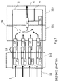
- Fig.3 represents a possible embodiment of a transmission system 1 according to the present invention.
- Said transmission system 1 comprises four input channels 3, also called tributaries, having each a bit rate of 10Gb/s. It has to be noted that the value of 10Gb/s and the number of four input channels 3 are given as examples (because of the general use of 10 and 40 Gb/s transmission links in the current communication networks) but any value may be used in the scope of the present invention.
- Said tributaries 3 are connected to parallel First In First Out (FIFO) inputs 9.
- An additional control data channel 11 provides the status (active or idle) of the input channels 3.
- Said control data channel 11 is connected to the activity detection means 15 of each FIFO inputs 9.
- the data of the active streams transmitted on the input channels 3 are received in the corresponding queues of the FIFO inputs 9.
- a predetermined number of bits 13, corresponding to the slot size, of each active FIFO queue is copied to the corresponding input 17 of a switch 19 at a clock rate of 10GHz.
- Said predetermined number of bits 13 depends on the configuration chosen and allow to select the optimal trade-off between buffer size (queue length) and clock frequency.
- the switch 19 scans sequentially the selected predetermined number of bits of each active input 17 and write said bits in an output FIFO queue 21.
- the scanning rate is equal to (40/n)GHz where n is the predetermined number of bits 13.
- the control data channel 11 is also connected to a frequency generator 23.
- the frequency generator 23 generates a clock signal 7 corresponding to the actual total bitrate, for example, in the present example with four active input streams of 10Gb/s, the generated clock signal is 4*10GHz, that is to say 40GHz.
- the data of the output FIFO queue 21 are therefore read out, multiplexed and transmitted to the output channel 5 at a 40Gb/s bitrate. If one of the input channels 3 becomes inactive, as it is the case in Fig.2 , the information of such inactivity (idle status) is brought by the control data channel to the transmission system 1. As a consequence, the switch 21 will only scan the three remaining active inputs 17 and the frequency generator 23 will generate a clock signal of 30GHz such that the data of the output FIFO queue 21 will be read out and transmitted to the output channel 5 at a 30Gb/s bitrate.
- variable bitrate optical transponder may be coupled to the output channel 5 in order to convert the electronic signal into a corresponding optical signal having the same bitrate.
- bitrate of the transmitted optical signal varies in function of the amount of data needed to be transmitted through the optical network.
- the signal After transmission through the communication network, the signal is received at the egress node.
- the signal In the case of an optical transmission network, the signal is converted to an electronic signal thanks to an optical transponder located at the input of the egress node.
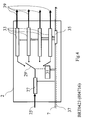
- Fig.4 represents a possible embodiment of a distributor or reception system 2.
- the operation achieved by said reception system 2 corresponds to the converse operation with respect to the transmission system 1 presented in Fig.3 .
- the transmitted signal is received on a FIFO input 27 through an input channel 25.
- the clock signal 7 is also transmitted and received at the reception system 2. Said clock signal 7 is transmitted to the FIFO input 27 in order to allow said input to process the received data.
- a control data channel 37 comprising information required for demultiplexing the received signals is connected to the reception system 2.
- Said information comprises, for example, the total bitrate, the number of active input channels and the slot size (number of bits used for the multiplexing).
- a switch controller 31 manages the position of the switch 29 in order to distribute the signal among the FIFO outputs 33.
- a clock signal (for example of 10GHz) generated by a clock generator 35 is distributed to the different FIFO outputs 33 in order to transmit the demultiplexed signals at the required bitrate (for example 10Gb/s) to the output channels 39.
- the switch controller 31 will send the first received byte to the first FIFO output 33, the second byte to the second FIFO output 33 and so on sequentially such that the four initial signals received at the four input channels 3 of the transmission system 1 will be recreated at the FIFO outputs 33.
- the signal received on the input channel 25 has a bitrate of 30 Gb/s and is composed of three active input channels. Said information is transmitted through the control data channel 37 and in the same way, the three signals will be recreated at the three corresponding output channels 39.
- the signals received on the different input channels 3 have different bitrates (for example 10Gb/s for the first two input channels and 5 Gb/s for the two following input channels) or different format corresponding to slightly different bitrates.
- the position of the switch 19 will be monitored in order to take into account the different bitrates such that the time spent by the switch in a position corresponds to the time required in function of the bitrate of the corresponding input channel 3.
- additional data (such as the individual bitrates) will be added in the control data signal 37 in order to allow the switch controller 31 and the switch 29 to correctly demultiplex the received signal.
- the clock generator 35 will have to generate individual clock signal for each signal in order to recreate the initial signal at the FIFO outputs 33.
- the operating bitrate of the output channel 5 is 30Gb/s and comprises four tributaries.
- the control data channel will then transmit said information to the reception system 2 in order to recreate the four signals with two signals having a 10Gb/s bitrate and two signals having a 5Gb/s bitrate at the output channels 39.
- the embodiments of the present invention allow to adapt the bitrate of transmitted signals in function of the number of active input channel signals.
- Such bitrate agility reduces the power consumption, allows adaptation of the network to the customers needs and eases the upgrade of the current networks to improved capacities.
- the reduction of the bitrate of the transmitted signal reduces signal impairments and therefore leads to a better signal quality.
Landscapes
- Engineering & Computer Science (AREA)
- Computer Networks & Wireless Communication (AREA)
- Signal Processing (AREA)
- Multimedia (AREA)
- Communication Control (AREA)
- Time-Division Multiplex Systems (AREA)
- Synchronisation In Digital Transmission Systems (AREA)
Abstract
- a parallel to serial conversion device comprising a plurality of parallel inputs and a serial output,
- a control unit comprising detection means adapted for detecting the activity of said plurality of parallel inputs of said parallel to serial conversion device, indication means adapted for indicating the active parallel inputs to the parallel to serial conversion device and controlling means adapted for setting an operating bitrate of the serial output in function of said activity of said plurality of parallel inputs.
Description
- The present invention relates to the field of communication networks and in particular to dynamic networks with bitrate agility.
Current communication networks comprises different types of transmission links having different bitrates. Thus, in order to reduce transmission costs while providing enhanced services, an idea is to aggregate a plurality of low bitrate data streams into a high bitrate data stream for high speed communications.
In the state of the art, concentrators allowing to aggregate several signals are known but the bitrate of the output transmission link is always the same whatever the number of received signals. Indeed, in case of inactive inputs, bit padding is achieved in order to compensate for the missing signal.
Thus, useless signals are transmitted which maximizes the required amount of energy and may lead to a reduced signal quality.
Besides, another solution for adapting the bitrate of the output port of a concentrator is to modify the Internet Protocol (IP) router so that it can deliver variable bitrates. However, such solution requires significant and expensive modifications and may lead to compatibility issues with existing routers. - It is therefore an object of the present invention to overcome the above cited drawbacks of the state of the art and provide a method allowing to aggregate a variable number of input low bitrate signals into an output signal with a variable high birate without requiring important modifications in the network design.
- Thus, the present invention refers to a signal concentrator comprising:
- a parallel to serial conversion device comprising a plurality of parallel inputs and a serial output,
- a control unit comprising detection means adapted for detecting the activity of said plurality of parallel inputs of said parallel to serial conversion device, indication means adapted for indicating the active parallel inputs to the parallel to serial conversion device and controlling means adapted for setting an operating bitrate of the serial output in function of said activity of said plurality of parallel inputs.
- According to another embodiment, the controlling means comprise a clock signal generator for generating a clock signal in function of the activity of said plurality of parallel inputs, said clock signal allowing the setting of the operating bitrate.
- According to a further embodiment, the plurality of parallel inputs of the parallel to serial conversion device are coupled to a plurality of fixed bitrate transmission lines and the activity detection of a parallel input comprises the detection of a received data signal at said parallel input.
- According to an additional embodiment, the transmission lines have the same bitrate.
- According to another embodiment, the operating bitrate of the serial output is determined by detecting the number of active parallel inputs.
- According to a further embodiment, the signals received by the parallel inputs have different bitrates and the control unit comprises determination means adapted to determine the bitrate of the received signals.
- According to an additional embodiment, the clock signal corresponds to the sum of the clock rates of the active parallel inputs.
- According to another embodiment, the parallel to serial conversion device comprises a First In First Out (FIFO) queue, the active parallel inputs are sequentially scanned and a predetermined number of bits of the signals received on said active parallel inputs is transmitted to the FIFO queue the output of which corresponds to the output of the parallel to serial conversion device.
- According to a further embodiment, the predetermined number of bits is equal to one.
- According to an additional embodiment, the predetermined number of bits corresponds to a byte.
- According to another embodiment, the predetermined number of bits corresponds to a frame.
- The present invention also refers to an optical transmission system comprising:
- a signal concentrator,
- a variable bitrate optical transponder coupled to the serial output of the parallel to serial conversion device.
- The present invention also refers to a signal distributor comprising
- a serial to parallel conversion device comprising a serial input and a plurality of parallel outputs,
- a control unit comprising detection means adapted for detecting the number of independent data signal comprised in the signal received at the serial input and the organization of said signals and controlling means adapted for distributing the signal received at the serial input towards said plurality of parallel inputs.
- The present invention also refers to an optical reception system comprising:
- a signal distributor,
- a variable bitrate optical transponder coupled to the serial input of the parallel to serial conversion device.
-
-
FIG.1 is a diagram representing a concentrator; -
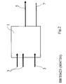
FIG.2 is a diagram representing a concentrator with an inactive input; -
FIG.3 is a diagram representing a possible embodiment of a concentrator according to the invention; -
FIG.4 is a diagram representing a possible embodiment of a receiver according to the invention; - As used herein, the term "active input" refers to an input receiving data signals;
- As used herein, the term "Gb/s" refers to the unit gigabit per second;
- As used herein, the term "GHz" refers to the unit gigahertz;
An embodiment of the present invention refers to a concentrator ortransmission system 1 as described inFig.1 allowing to aggregate the signals received on a plurality ofparallel input channels 3 onto aserial output channel 5 having a bitrate equal to the sum of the bitrates of theinput channels 3. InFig. 1 , the transmission system comprises fourinput channels 3 having each a 10Gb/s bitrate such that theoutput channel 5 has a 40Gb/s bitrate. Moreover, aclock signal 7 corresponding to the bitrate of the output channel (40 GHz in the present case) is provided. Besides, if only three of theinput channels 3 are active as represented inFig.2 , the bitrate of theoutput channel 5 becomes 30Gb/s corresponding to aclock signal 7 of 30GHz. In addition, an adaptation of the bitrate to the actual needs allows to save energy and to improve the signal quality when the bit rate is reduced.
Fig.3 represents a possible embodiment of atransmission system 1 according to the present invention. Saidtransmission system 1 comprises fourinput channels 3, also called tributaries, having each a bit rate of 10Gb/s.
It has to be noted that the value of 10Gb/s and the number of fourinput channels 3 are given as examples (because of the general use of 10 and 40 Gb/s transmission links in the current communication networks) but any value may be used in the scope of the present invention.
Saidtributaries 3 are connected to parallel First In First Out (FIFO)inputs 9. An additionalcontrol data channel 11 provides the status (active or idle) of theinput channels 3. Saidcontrol data channel 11 is connected to the activity detection means 15 of eachFIFO inputs 9. In thefirst section 101 of thetransmission system 1, the data of the active streams transmitted on theinput channels 3 are received in the corresponding queues of theFIFO inputs 9. Then, a predetermined number ofbits 13, corresponding to the slot size, of each active FIFO queue is copied to thecorresponding input 17 of aswitch 19 at a clock rate of 10GHz.
Said predetermined number ofbits 13 depends on the configuration chosen and allow to select the optimal trade-off between buffer size (queue length) and clock frequency. It can be, for example, a bit per bit, a byte per byte or a frame per frame selection.
Insection 102, theswitch 19 scans sequentially the selected predetermined number of bits of eachactive input 17 and write said bits in anoutput FIFO queue 21. The scanning rate is equal to (40/n)GHz where n is the predetermined number ofbits 13.
Besides, thecontrol data channel 11 is also connected to afrequency generator 23. Thus, atstep 103, thefrequency generator 23 generates aclock signal 7 corresponding to the actual total bitrate, for example, in the present example with four active input streams of 10Gb/s, the generated clock signal is 4*10GHz, that is to say 40GHz.
The data of theoutput FIFO queue 21 are therefore read out, multiplexed and transmitted to theoutput channel 5 at a 40Gb/s bitrate.
If one of theinput channels 3 becomes inactive, as it is the case inFig.2 , the information of such inactivity (idle status) is brought by the control data channel to thetransmission system 1. As a consequence, theswitch 21 will only scan the three remainingactive inputs 17 and thefrequency generator 23 will generate a clock signal of 30GHz such that the data of theoutput FIFO queue 21 will be read out and transmitted to theoutput channel 5 at a 30Gb/s bitrate. - Besides, in the case of an optical network, a variable bitrate optical transponder may be coupled to the
output channel 5 in order to convert the electronic signal into a corresponding optical signal having the same bitrate. Thus, the bitrate of the transmitted optical signal varies in function of the amount of data needed to be transmitted through the optical network. - After transmission through the communication network, the signal is received at the egress node. In the case of an optical transmission network, the signal is converted to an electronic signal thanks to an optical transponder located at the input of the egress node.
Fig.4 represents a possible embodiment of a distributor orreception system 2. The operation achieved by saidreception system 2 corresponds to the converse operation with respect to thetransmission system 1 presented inFig.3 .
The transmitted signal is received on aFIFO input 27 through aninput channel 25. Theclock signal 7 is also transmitted and received at thereception system 2. Saidclock signal 7 is transmitted to theFIFO input 27 in order to allow said input to process the received data. In addition, acontrol data channel 37 comprising information required for demultiplexing the received signals is connected to thereception system 2. Said information comprises, for example, the total bitrate, the number of active input channels and the slot size (number of bits used for the multiplexing). Based on this information and using theclock signal 7, aswitch controller 31 manages the position of theswitch 29 in order to distribute the signal among the FIFO outputs 33. A clock signal (for example of 10GHz) generated by aclock generator 35 is distributed to the different FIFO outputs 33 in order to transmit the demultiplexed signals at the required bitrate (for example 10Gb/s) to theoutput channels 39. - Based on the previous example, if the received signal has a bitrate of 40Gb/s and is composed of four active input channels which have a slot size of one byte, then the
switch controller 31 will send the first received byte to thefirst FIFO output 33, the second byte to thesecond FIFO output 33 and so on sequentially such that the four initial signals received at the fourinput channels 3 of thetransmission system 1 will be recreated at the FIFO outputs 33. In the case described inFig.2 , the signal received on theinput channel 25 has a bitrate of 30 Gb/s and is composed of three active input channels. Said information is transmitted through thecontrol data channel 37 and in the same way, the three signals will be recreated at the threecorresponding output channels 39. - According to another embodiment, the signals received on the
different input channels 3 have different bitrates (for example 10Gb/s for the first two input channels and 5 Gb/s for the two following input channels) or different format corresponding to slightly different bitrates. In such situation, the position of theswitch 19 will be monitored in order to take into account the different bitrates such that the time spent by the switch in a position corresponds to the time required in function of the bitrate of thecorresponding input channel 3. Moreover, additional data (such as the individual bitrates) will be added in the control data signal 37 in order to allow theswitch controller 31 and theswitch 29 to correctly demultiplex the received signal. Besides, theclock generator 35 will have to generate individual clock signal for each signal in order to recreate the initial signal at the FIFO outputs 33. Thus with two input channels of 10Gb/s and two channels of 5Gb/s, when all theinput channels 3 are active, the operating bitrate of theoutput channel 5 is 30Gb/s and comprises four tributaries. The control data channel will then transmit said information to thereception system 2 in order to recreate the four signals with two signals having a 10Gb/s bitrate and two signals having a 5Gb/s bitrate at theoutput channels 39. - As a conclusion, the embodiments of the present invention allow to adapt the bitrate of transmitted signals in function of the number of active input channel signals. Such bitrate agility reduces the power consumption, allows adaptation of the network to the customers needs and eases the upgrade of the current networks to improved capacities. Moreover, the reduction of the bitrate of the transmitted signal reduces signal impairments and therefore leads to a better signal quality.
Claims (14)
- Signal concentrator (1) comprising:- a parallel to serial conversion device comprising a plurality of parallel inputs (3) and a serial output (5),- a control unit comprising detection means adapted for detecting the activity of said plurality of parallel inputs of said parallel to serial conversion device, indication means adapted for indicating the active parallel inputs to the parallel to serial conversion device and controlling means adapted for setting an operating bitrate of the serial output in function of said activity of said plurality of parallel inputs.
- Signal concentrator (1) in accordance with claim 1 wherein said controlling means comprise a clock signal generator (23) for generating a clock signal in function of the activity of said plurality of parallel inputs, said clock signal allowing the setting of the operating bitrate.
- Signal concentrator (1) in accordance with claim 1 or 2 wherein the plurality of parallel inputs (3) of the parallel to serial conversion device are coupled to a plurality of fixed bitrate transmission lines and wherein the activity detection of a parallel input comprises the detection of a received data signal at said parallel input.
- Signal concentrator (1) in accordance with claim 3 wherein the transmission lines have the same bitrate.
- Signal concentrator (1) in accordance with claim 4 wherein the operating bitrate of the serial output (5) is determined by detecting the number of active parallel inputs (3).
- Signal concentrator (1) in accordance with claim 2 wherein the signals received by the parallel inputs (3) have different bitrates and wherein the control unit comprises determination means adapted to determine the bitrate of the received signals.
- Signal concentrator (1) in accordance with claims 2 and 6 wherein the clock signal corresponds to the sum of the clock rates of the active parallel inputs.
- Signal concentrator (1) in accordance with one of the previous claims wherein the parallel to serial conversion device comprises a First In First Out (FIFO) queue and wherein the active parallel inputs are sequentially scanned and a predetermined number of bits of the signals received on said active parallel inputs is transmitted to the FIFO queue the output of which corresponds to the output of the parallel to serial conversion device.
- Signal concentrator (1) in accordance with claim 8 wherein the predetermined number of bits is equal to one.
- Signal concentrator (1) in accordance with claim 8 wherein the predetermined number of bits corresponds to a byte.
- Signal concentrator (1) in accordance with claim 8 wherein the predetermined number of bits corresponds to a frame.
- Optical transmission system comprising:- a signal concentrator (1) according to one of the previous claims,- a variable bitrate optical transponder coupled to the serial output of the parallel to serial conversion device.
- Signal distributor 2 comprising- a serial to parallel conversion device comprising a serial input and a plurality of parallel outputs,- a control unit comprising detection means adapted for detecting the number of independent data signal comprised in the signal received at the serial input and the organization of said signals and controlling means adapted for distributing the signal received at the serial input towards said plurality of parallel inputs.
- Optical reception system comprising:- a signal distributor according to claim 13,- a variable bitrate optical transponder coupled to the serial input of the parallel to serial conversion device.
Priority Applications (6)
| Application Number | Priority Date | Filing Date | Title |
|---|---|---|---|
| EP09290441A EP2262139A1 (en) | 2009-06-12 | 2009-06-12 | Variable bitrate equipment |
| CN201080025892.0A CN102804653B (en) | 2009-06-12 | 2010-03-03 | Variable bitrate equipment |
| US13/319,236 US8624762B2 (en) | 2009-06-12 | 2010-03-03 | Variable bitrate equipment |
| KR1020117029478A KR20120026531A (en) | 2009-06-12 | 2010-03-03 | Variable bitrate device |
| JP2012514399A JP5558564B2 (en) | 2009-06-12 | 2010-03-03 | Variable bit rate equipment |
| PCT/EP2010/052664 WO2010142472A1 (en) | 2009-06-12 | 2010-03-03 | Variable bitrate equipment |
Applications Claiming Priority (1)
| Application Number | Priority Date | Filing Date | Title |
|---|---|---|---|
| EP09290441A EP2262139A1 (en) | 2009-06-12 | 2009-06-12 | Variable bitrate equipment |
Publications (1)
| Publication Number | Publication Date |
|---|---|
| EP2262139A1 true EP2262139A1 (en) | 2010-12-15 |
Family
ID=41278116
Family Applications (1)
| Application Number | Title | Priority Date | Filing Date |
|---|---|---|---|
| EP09290441A Withdrawn EP2262139A1 (en) | 2009-06-12 | 2009-06-12 | Variable bitrate equipment |
Country Status (6)
| Country | Link |
|---|---|
| US (1) | US8624762B2 (en) |
| EP (1) | EP2262139A1 (en) |
| JP (1) | JP5558564B2 (en) |
| KR (1) | KR20120026531A (en) |
| CN (1) | CN102804653B (en) |
| WO (1) | WO2010142472A1 (en) |
Families Citing this family (6)
| Publication number | Priority date | Publication date | Assignee | Title |
|---|---|---|---|---|
| US9088422B2 (en) * | 2010-06-04 | 2015-07-21 | Broadcom Corporation | Method and system for energy efficient based service optimization by a broadband gateway |
| KR20110129823A (en) * | 2010-05-26 | 2011-12-02 | 한국전자통신연구원 | Device for transmitting and receiving data in communication system |
| EP2912893B1 (en) * | 2012-10-25 | 2019-09-04 | Telefonaktiebolaget LM Ericsson (publ) | Method and power adaptation device arranged to adjust power consumption in a network node |
| US9438369B2 (en) | 2014-05-19 | 2016-09-06 | Ciena Corporation | Margin-based optimization systems and methods in optical networks for capacity boosting |
| US11476949B2 (en) | 2018-03-29 | 2022-10-18 | Cable Television Laboratories, Inc. | Systems and methods for coherent optics in an access network |
| US10587339B1 (en) | 2018-11-27 | 2020-03-10 | Ciena Corporation | Systems and methods for achieving best effort home route capacity on protection paths during optical restoration |
Citations (4)
| Publication number | Priority date | Publication date | Assignee | Title |
|---|---|---|---|---|
| US4429383A (en) * | 1980-01-16 | 1984-01-31 | Siemens Aktiengesellschaft | Method for seizing time slots of a time-division multiplex system with dynamic multiplexers |
| DE19536025C1 (en) * | 1995-09-27 | 1997-02-20 | Siemens Ag | Method and data transmission system for selectively transmitting one or more data signal streams over a time-division multiplex transmission medium |
| WO2000027060A1 (en) * | 1998-11-02 | 2000-05-11 | Koninklijke Philips Electronics N.V. | Communication system using a multiplex signal carrying an auxiliary signal |
| WO2000044175A1 (en) * | 1999-01-22 | 2000-07-27 | Scientific-Atlanta, Inc. | Method and apparatus for delivering reference signal information within a specified time interval |
Family Cites Families (20)
| Publication number | Priority date | Publication date | Assignee | Title |
|---|---|---|---|---|
| US4685101A (en) * | 1984-12-20 | 1987-08-04 | Siemens Aktiengesellschaft | Digital multiplexer for PCM voice channels having a cross-connect capability |
| JPH0427230A (en) * | 1990-05-22 | 1992-01-30 | Nec Corp | Communication equipment for digital auxiliary signal |
| JPH0575566A (en) * | 1991-09-10 | 1993-03-26 | Fujitsu Ltd | Signal multiplexer |
| SE503702C2 (en) * | 1993-10-12 | 1996-08-05 | Ericsson Telefon Ab L M | Signal processing unit which converts input transmission rate to a separate output transmission rate therefrom |
| JP2933480B2 (en) * | 1993-12-21 | 1999-08-16 | 日本電気株式会社 | Time division multiplex signal transmission equipment |
| JPH11331305A (en) * | 1998-05-08 | 1999-11-30 | Sony Corp | Transmission device and transmission method, reception device and reception method, and providing medium |
| JP3299933B2 (en) * | 1998-11-16 | 2002-07-08 | 日本電信電話株式会社 | Optical time division multiplex terminal equipment |
| US6631144B1 (en) * | 1999-12-21 | 2003-10-07 | Intel Corporation | Multi-rate transponder system and chip set |
| US7366267B1 (en) * | 2001-03-07 | 2008-04-29 | Altera Corporation | Clock data recovery with double edge clocking based phase detector and serializer/deserializer |
| US20040102874A1 (en) * | 2002-11-27 | 2004-05-27 | Crosby Philip S. | Method and apparatus for controlling an optical transponder |
| JP4062522B2 (en) * | 2003-03-11 | 2008-03-19 | 横河電機株式会社 | Optical signal processing device |
| JP4364068B2 (en) * | 2003-11-14 | 2009-11-11 | 富士通株式会社 | Signal distribution method and apparatus |
| US7342520B1 (en) * | 2004-01-08 | 2008-03-11 | Vladimir Katzman | Method and system for multilevel serializer/deserializer |
| US7817068B2 (en) * | 2006-06-30 | 2010-10-19 | Intel Corporation | Low power serial link bus architecture |
| JP5076454B2 (en) * | 2006-11-15 | 2012-11-21 | 富士通セミコンダクター株式会社 | Serial data receiving circuit, serial data receiving device, and serial data receiving method |
| US7835393B2 (en) * | 2008-01-16 | 2010-11-16 | Applied Micro Circuits Corporation | System and method for converting multichannel time division multiplexed data into packets |
| US7986878B2 (en) * | 2008-02-05 | 2011-07-26 | Opnext Subsystems, Inc. | Adjustable bit rate optical transmission using programmable signal modulation |
| WO2010053070A1 (en) * | 2008-11-05 | 2010-05-14 | 日本電気株式会社 | Electronic circuit system, track hold circuit module, electronic circuit operation control method, and program thereof |
| US8188894B2 (en) * | 2009-06-30 | 2012-05-29 | Infinera Corporation | Devices for conversion between serial and parallel data |
| JP5426604B2 (en) * | 2011-04-26 | 2014-02-26 | 富士通テレコムネットワークス株式会社 | Optical packet switching system |
-
2009
- 2009-06-12 EP EP09290441A patent/EP2262139A1/en not_active Withdrawn
-
2010
- 2010-03-03 JP JP2012514399A patent/JP5558564B2/en not_active Expired - Fee Related
- 2010-03-03 KR KR1020117029478A patent/KR20120026531A/en not_active Ceased
- 2010-03-03 WO PCT/EP2010/052664 patent/WO2010142472A1/en not_active Ceased
- 2010-03-03 US US13/319,236 patent/US8624762B2/en not_active Expired - Fee Related
- 2010-03-03 CN CN201080025892.0A patent/CN102804653B/en not_active Expired - Fee Related
Patent Citations (4)
| Publication number | Priority date | Publication date | Assignee | Title |
|---|---|---|---|---|
| US4429383A (en) * | 1980-01-16 | 1984-01-31 | Siemens Aktiengesellschaft | Method for seizing time slots of a time-division multiplex system with dynamic multiplexers |
| DE19536025C1 (en) * | 1995-09-27 | 1997-02-20 | Siemens Ag | Method and data transmission system for selectively transmitting one or more data signal streams over a time-division multiplex transmission medium |
| WO2000027060A1 (en) * | 1998-11-02 | 2000-05-11 | Koninklijke Philips Electronics N.V. | Communication system using a multiplex signal carrying an auxiliary signal |
| WO2000044175A1 (en) * | 1999-01-22 | 2000-07-27 | Scientific-Atlanta, Inc. | Method and apparatus for delivering reference signal information within a specified time interval |
Also Published As
| Publication number | Publication date |
|---|---|
| US20120249347A1 (en) | 2012-10-04 |
| KR20120026531A (en) | 2012-03-19 |
| WO2010142472A1 (en) | 2010-12-16 |
| CN102804653A (en) | 2012-11-28 |
| JP2012529817A (en) | 2012-11-22 |
| US8624762B2 (en) | 2014-01-07 |
| CN102804653B (en) | 2016-06-29 |
| JP5558564B2 (en) | 2014-07-23 |
Similar Documents
| Publication | Publication Date | Title |
|---|---|---|
| EP3036869B1 (en) | Reconfigurable and variable-rate shared multi-transponder architecture for flexible ethernet-based optical networks | |
| EP2683102B1 (en) | Device and Method for transmitting samples of a digital baseband signal | |
| US20210243668A1 (en) | Radio Link Aggregation | |
| US8624762B2 (en) | Variable bitrate equipment | |
| JP4844219B2 (en) | Optical network and node | |
| US8867538B2 (en) | Ethernet media converter supporting high-speed wireless access | |
| JP6126598B2 (en) | Circuit apparatus and method for transmitting signals | |
| JP5806408B2 (en) | Access node for communication network | |
| EP4412239B1 (en) | Control of onu activation in high bit rate pons | |
| WO2021057363A1 (en) | State control method, data sending method, and terminal | |
| WO2002098162A1 (en) | A method based on backboard transmitting time division multiplexing circuit data and a bridge connector | |
| KR20130048091A (en) | Apparatus and method for operating multi lane in high-rate ethernet optical link interface | |
| JP2008502192A (en) | Backpressure method for multiplexed links | |
| JP2001103028A (en) | Signal multiplexing method | |
| WO2019122881A1 (en) | Data communication | |
| JP5071693B2 (en) | Communication apparatus, communication system, and communication speed switching method | |
| US8730792B2 (en) | Switching device and switching method | |
| EP2273702A1 (en) | Adaptive optical transmission equipment | |
| GB2422497A (en) | Asymmetric bidirectional wavelength division multiplexing | |
| JP2006067354A (en) | PON system and TDM signal transmission method | |
| KR100498939B1 (en) | TDM Method of Broadcasting Signals and Telecommunication Signals in Broadcasting and Communication Convergence System | |
| CN101997631A (en) | Method and system for transmitting non-service information as well as equipment for sending and receiving non-service information | |
| WO2025248768A1 (en) | Communication system and communication method | |
| CN106559353A (en) | The transmit queue dynamic adjusting method of many CES channels in a kind of PTN | |
| KR100452514B1 (en) | A matching device of dual mode ds3 circuit network for atm exchange |
Legal Events
| Date | Code | Title | Description |
|---|---|---|---|
| PUAI | Public reference made under article 153(3) epc to a published international application that has entered the european phase |
Free format text: ORIGINAL CODE: 0009012 |
|
| AK | Designated contracting states |
Kind code of ref document: A1 Designated state(s): AT BE BG CH CY CZ DE DK EE ES FI FR GB GR HR HU IE IS IT LI LT LU LV MC MK MT NL NO PL PT RO SE SI SK TR |
|
| AX | Request for extension of the european patent |
Extension state: AL BA RS |
|
| 17P | Request for examination filed |
Effective date: 20110615 |
|
| RAP1 | Party data changed (applicant data changed or rights of an application transferred) |
Owner name: ALCATEL LUCENT |
|
| 111Z | Information provided on other rights and legal means of execution |
Free format text: AT BE BG CH CY CZ DE DK EE ES FI FR GB GR HR HU IE IS IT LI LT LU LV MC MK MT NL NO PL PT RO SE SI SK TR Effective date: 20130410 |
|
| RAP1 | Party data changed (applicant data changed or rights of an application transferred) |
Owner name: ALCATEL LUCENT |
|
| D11X | Information provided on other rights and legal means of execution (deleted) | ||
| 17Q | First examination report despatched |
Effective date: 20170614 |
|
| GRAP | Despatch of communication of intention to grant a patent |
Free format text: ORIGINAL CODE: EPIDOSNIGR1 |
|
| INTG | Intention to grant announced |
Effective date: 20180205 |
|
| RAP1 | Party data changed (applicant data changed or rights of an application transferred) |
Owner name: ALCATEL LUCENT |
|
| STAA | Information on the status of an ep patent application or granted ep patent |
Free format text: STATUS: THE APPLICATION IS DEEMED TO BE WITHDRAWN |
|
| 18D | Application deemed to be withdrawn |
Effective date: 20180616 |