EP2261617A1 - Photodetector - Google Patents
Photodetector Download PDFInfo
- Publication number
- EP2261617A1 EP2261617A1 EP09723540A EP09723540A EP2261617A1 EP 2261617 A1 EP2261617 A1 EP 2261617A1 EP 09723540 A EP09723540 A EP 09723540A EP 09723540 A EP09723540 A EP 09723540A EP 2261617 A1 EP2261617 A1 EP 2261617A1
- Authority
- EP
- European Patent Office
- Prior art keywords
- substrate
- film
- bolometer
- metal
- metal film
- Prior art date
- Legal status (The legal status is an assumption and is not a legal conclusion. Google has not performed a legal analysis and makes no representation as to the accuracy of the status listed.)
- Granted
Links
Images







Classifications
-
- G—PHYSICS
- G01—MEASURING; TESTING
- G01J—MEASUREMENT OF INTENSITY, VELOCITY, SPECTRAL CONTENT, POLARISATION, PHASE OR PULSE CHARACTERISTICS OF INFRARED, VISIBLE OR ULTRAVIOLET LIGHT; COLORIMETRY; RADIATION PYROMETRY
- G01J5/00—Radiation pyrometry, e.g. infrared or optical thermometry
- G01J5/02—Constructional details
- G01J5/08—Optical arrangements
- G01J5/0853—Optical arrangements having infrared absorbers other than the usual absorber layers deposited on infrared detectors like bolometers, wherein the heat propagation between the absorber and the detecting element occurs within a solid
-
- H—ELECTRICITY
- H10—SEMICONDUCTOR DEVICES; ELECTRIC SOLID-STATE DEVICES NOT OTHERWISE PROVIDED FOR
- H10F—INORGANIC SEMICONDUCTOR DEVICES SENSITIVE TO INFRARED RADIATION, LIGHT, ELECTROMAGNETIC RADIATION OF SHORTER WAVELENGTH OR CORPUSCULAR RADIATION
- H10F39/00—Integrated devices, or assemblies of multiple devices, comprising at least one element covered by group H10F30/00, e.g. radiation detectors comprising photodiode arrays
- H10F39/10—Integrated devices
- H10F39/107—Integrated devices having multiple elements covered by H10F30/00 in a repetitive configuration, e.g. radiation detectors comprising photodiode arrays
-
- G—PHYSICS
- G01—MEASURING; TESTING
- G01J—MEASUREMENT OF INTENSITY, VELOCITY, SPECTRAL CONTENT, POLARISATION, PHASE OR PULSE CHARACTERISTICS OF INFRARED, VISIBLE OR ULTRAVIOLET LIGHT; COLORIMETRY; RADIATION PYROMETRY
- G01J5/00—Radiation pyrometry, e.g. infrared or optical thermometry
- G01J5/10—Radiation pyrometry, e.g. infrared or optical thermometry using electric radiation detectors
- G01J5/20—Radiation pyrometry, e.g. infrared or optical thermometry using electric radiation detectors using resistors, thermistors or semiconductors sensitive to radiation, e.g. photoconductive devices
-
- G—PHYSICS
- G01—MEASURING; TESTING
- G01J—MEASUREMENT OF INTENSITY, VELOCITY, SPECTRAL CONTENT, POLARISATION, PHASE OR PULSE CHARACTERISTICS OF INFRARED, VISIBLE OR ULTRAVIOLET LIGHT; COLORIMETRY; RADIATION PYROMETRY
- G01J5/00—Radiation pyrometry, e.g. infrared or optical thermometry
- G01J5/10—Radiation pyrometry, e.g. infrared or optical thermometry using electric radiation detectors
- G01J5/20—Radiation pyrometry, e.g. infrared or optical thermometry using electric radiation detectors using resistors, thermistors or semiconductors sensitive to radiation, e.g. photoconductive devices
- G01J5/22—Electrical features thereof
- G01J5/24—Use of specially adapted circuits, e.g. bridge circuits
-
- H—ELECTRICITY
- H10—SEMICONDUCTOR DEVICES; ELECTRIC SOLID-STATE DEVICES NOT OTHERWISE PROVIDED FOR
- H10F—INORGANIC SEMICONDUCTOR DEVICES SENSITIVE TO INFRARED RADIATION, LIGHT, ELECTROMAGNETIC RADIATION OF SHORTER WAVELENGTH OR CORPUSCULAR RADIATION
- H10F39/00—Integrated devices, or assemblies of multiple devices, comprising at least one element covered by group H10F30/00, e.g. radiation detectors comprising photodiode arrays
- H10F39/10—Integrated devices
- H10F39/12—Image sensors
- H10F39/191—Photoconductor image sensors
- H10F39/193—Infrared image sensors
-
- H—ELECTRICITY
- H10—SEMICONDUCTOR DEVICES; ELECTRIC SOLID-STATE DEVICES NOT OTHERWISE PROVIDED FOR
- H10F—INORGANIC SEMICONDUCTOR DEVICES SENSITIVE TO INFRARED RADIATION, LIGHT, ELECTROMAGNETIC RADIATION OF SHORTER WAVELENGTH OR CORPUSCULAR RADIATION
- H10F99/00—Subject matter not provided for in other groups of this subclass
-
- H—ELECTRICITY
- H10—SEMICONDUCTOR DEVICES; ELECTRIC SOLID-STATE DEVICES NOT OTHERWISE PROVIDED FOR
- H10N—ELECTRIC SOLID-STATE DEVICES NOT OTHERWISE PROVIDED FOR
- H10N15/00—Thermoelectric devices without a junction of dissimilar materials; Thermomagnetic devices, e.g. using the Nernst-Ettingshausen effect
Definitions
- the present invention relates to a photodetector.
- Patent Document 1 has disclosed that which is provided with a bolometer element for detecting infrared rays made incident and a reference element for detecting temperature variation caused by variation in use environment, in which signals output by these elements are used to calculate signals excluding the influence of temperature variation caused by variation in use environment, thereby detecting infrared rays.
- Patent Document 1 Japanese Unexamined Patent Application Publication No. 10-227689*2 ( JP10227689A )
- the sacrifice layer of the reference element is made thin in an attempt to enhance response to temperature variation in use environment, such a constitution is obtained that is greatly different in height between the bolometer element and the reference element.
- depth of focus is difficult to control and formation of minute patterns is made difficult, which may hinder downsizing of the infrared detector.
- the present invention has been made in order to solve the above-described technical problems, an object of which is to provide a photodetector capable of achieving downsizing while sufficiently reducing the influence of temperature variation in use environment.
- a photodetector of the present invention is constituted with a first bolometer film which is supported on a surface of a substrate while spaced apart from the surface of the substrate, a second bolometer film which is supported on the surface of the substrate while spaced apart from the surface of the substrate and, a metal film for heat dissipation formed on a surface of the bolometer thin film via an insulating film, wherein the surface of the bolometer thin film faces the substrate, and a plurality of metal columns connected thermally with the first metal film and the substrate.
- the second bolometer film is connected with the substrate. Therefore, where the second bolometer film is adopted as a bolometer film of the reference element, heat of the second bolometer film generated by infrared rays is efficiently dissipated to the substrate via the insulating film, the first metal film and the metal columns, thus making it possible to measure accurately only the temperature variation caused by variation in use environment. As a result, it is possible to efficiently reduce the influence of temperature variation in use environment. Further, there is no need to make the sacrifice layer thickness thin for efficiently dissipating heat of the reference element to the substrate. Thereby, for example, upon patterning by exposure to light, depth of focus is controlled easily and minute patterning is formed easily, consequently making it possible to achieve downsizing.
- the second metal film is formed at a region facing the second bolometer film on the surface of the substrate and the metal columns are connected with the first metal film and the second metal film.
- the second metal film is placed between the metal columns and the substrate, thereby where the second bolometer film is adopted as a bolometer film of the reference element, it is possible to increase a thermal contact area of the metal columns with the substrate.
- infrared rays made incident can be used to dissipate more efficiently heat generated at the second bolometer film to the substrate.
- a third metal film is formed at a region facing the first bolometer film on the surface of the substrate. This constitution is obtained, thereby where the first bolometer film is adopted as a bolometer film of the bolometer element, infrared rays transmitted through the first bolometer film are reflected on the first bolometer film by the third metal film and made incident again to the first bolometer film. Therefore, it is possible to efficiently measure heat generated by infrared rays.
- first bolometer film and the second bolometer film are located so as to be approximately in parallel with the surface of the substrate and approximately flush with each other.
- the above constitution is obtained, by which, for example, upon patterning by exposure to light, depth of focus can be controlled more easily.
- a photodetector capable of achieving downsizing while efficiently reducing the influence of temperature variation in use environment.
- a photodetector of the embodiment of the present invention is a so-called bolometer-type infrared detector for detecting infrared rays by the use of a material, the resistance value of which will vary depending on a temperature and favorably used in an infrared imager, thermography etc.
- Fig. 1 is a plan view of an infrared detector which is one embodiment of a photodetector according to the present invention.
- Fig. 2 is a partially enlarged plan view of a pixel portion of the infrared detector of Fig. 1 .
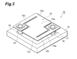
- FIG. 3 is a perspective view showing a constitution of one pixel of the infrared detector of Fig. 1 .
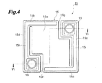
- Fig. 4 is a plan view showing a constitution of one pixel at a pixel portion of the infrared detector of Fig. 1 .
- Fig. 5 is a plan view showing a constitution of one pixel at a reference pixel portion of the infrared detector given in Fig. 1 .
- Fig. 6 is a schematic cross sectional view of the infrared detector in combination of a cross section taken along line VI - VI of Fig. 4 with that taken along line VI - VI of Fig. 5 .
- an infrared detector 1 is a detector for detecting infrared rays by thermal variation and constituted with a substrate 10, a pixel portion 12 which is formed on the substrate 10 to function as an infrared rays receiving unit, a reference pixel portion 13 which is formed on the substrate 10 to measure the influence by use environment, and a signal processing circuit portion 14.
- the pixel portion 12 and the reference pixel portion 13 are respectively connected electrically with the signal processing circuit portion 14.
- the substrate 10 for example, a Si substrate is used. It is noted that hereinafter, where a thermally oxidized layer and a base layer are formed on the surface of the Si substrate, the substrate containing these layers is referred to as the substrate 10.
- the pixel portion 12 is formed by arraying two-dimensionally a plurality of pixels (bolometer element 11) on the substrate 10 and referred to as a so-called surface micro-machine.
- the bolometer element 11 constituting pixels is, as shown in Fig. 3 and Fig. 4 , provided with ROIC (Read Only IC) pads 16, 17 formed on the surface of substrate 10, electrode plugs 18, 19 respectively formed on the ROIC pads 16, 17 and a bolometer thin film (first bolometer film) 15 arranged apart from the surface of the substrate 10.
- ROIC Read Only IC
- the ROIC pads 16, 17 are rectangular pads having electrical conductivity and connected electrically with the signal processing circuit portion 14.
- the electrode plugs 18, 19 are formed on the ROIC pads 16, 17 approximately in a column shape so as to extend in a laminated direction, and electrically connected with the ROIC pads 16, 17.
- the electrode plugs 18, 19 are made with a material with electrical conductivity, for example, Al is used.
- the bolometer thin film 15 is a thin film arranged approximately in parallel with the substrate 10 and provided with a photodetecting portion 15a which receives infrared rays and is formed in a rectangular planar-surface shape, and beam portions 15d, 15e formed at corners 15b, 15c of the photodetecting portion 15a.
- the beam portions 15d, 15e extend from the corners 15b, 15c along an outer periphery of the photodetecting portion 15a and formed so as to face each other. Then, clearances between the photodetecting portion 15a and the beam portions 15d, 15e are spatially apart via slits 15f, 15g respectively and thermally separated.
- the bolometer thin film 15 is made with a material great in specific resistance variation caused by temperature variation, for example, amorphous silicon is used.
- the bolometer thin film 15 is supported on the surface of the substrate 10 by one-end portions of the beam portions 15d, 15e which are respectively connected with the electrode plugs 18, 19. Between the bolometer thin film 15 and the substrate 10, there is formed a void space 11a. Then, as shown in Fig. 4 , the wires 15h, 15i of the beam portions 15d, 15e are electrically connected with electrode plugs 18, 19, respectively. Thereby, the wires 15h, 15i are electrically connected via the electrode plugs 18, 19 and the ROIC pads 16, 17 with the signal processing circuit portion 14.
- an insulating film 30 is formed on a surface of the bolometer thin film 15 facing the substrate 10.
- the insulating film 30 for example, a silicon-oxidized film is used which is based on TEOS (Tetraethyl orthosilicate) and formed by a plasma CVD (Chemical Vapor Deposition) method.
- TEOS Tetraethyl orthosilicate
- plasma CVD Chemical Vapor Deposition
- the bolometer element 11 is constituted in such a manner that the bolometer thin film 15 is apart from the surface of the substrate 10 and arranged approximately in parallel with the substrate 10 (membrane constitution), and a clearance between the bolometer thin film 15 and the substrate 10 is spatially apart by the void space 11a and thermally separated. Then, such a constitution is provided that specific resistance variation caused by temperature variation at the photodetecting portion 15a of the bolometer thin film 15 is read via the wires 15h, 15i, the electrode plugs 18, 19 and ROIC pads 16, 17 at the signal processing circuit portion 14.
- the reference pixel portion 13 is formed by arraying two-dimensionally a plurality of pixels (reference element 21) on the substrate 10, and each of the pixels is given as a so-called optical black.
- the pixel-constituting reference element 21 is, as shown in Fig. 5 and Fig. 6 , constituted so as to be substantially similar to the bolometer element 11, but different from the bolometer element 11 in that it is provided with a metal film for heat dissipation (first metal film) 23, a metal film for heat dissipation on the side of a substrate (second metal film) 24 and a plurality of metal columns 25. It is noted that a description will be omitted for the ROIC pads 26, 27 and the electrode plugs 28, 29 which are constituted in the same manner as the bolometer element 11.
- the bolometer thin film (second bolometer film) 22 has a similar constitution to the bolometer thin film 15 and is provided with a photodetecting portion 22a, beam portions 22d, 22e, wires 22h, 22i and slits 22f, 22g. Then, as shown in Fig. 6 , the bolometer thin film 22 and the bolometer thin film 15 are approximately in parallel with the surface of the substrate 10 and located so as to be approximately flush with each other.
- being approximately flush means a planar surface in such a range that includes a difference in thickness of a metal film 23 for heat dissipation to be described later in a laminating direction, for example, a planar surface within a range of approximately ⁇ 1 ⁇ m.
- a rectangular planar surface-shaped metal film 23 for heat dissipation via an insulating film 31 is formed on a surface of the photodetecting portion 22a facing the substrate 10.
- the insulating film 31 is constituted with a material similar to that of the insulating film 30 of the bolometer element 11.
- the metal film 23 for heat dissipation for example, Al, Cu or W is used.
- the metal columns 25 which are columns made with a metal and extending in a laminating direction are formed apart at constant intervals in a direction orthogonal to the laminating direction.
- the metal columns 25 are thermally connected with the metal film 23 for heat dissipation and the substrate 10.
- the metal columns 25 for example, Al, Cu or W is used. It is noted that the metal columns 25 may be formed integrally with the metal film 23 for heat dissipation.
- a rectangular planar surface-shaped metal film 24 for heat dissipation on the side of the substrate is formed at a region facing the photodetecting portion 22a of the bolometer thin film 22, on a surface of the reference element 21 facing the substrate 10.
- the metal film 24 for heat dissipation on the side of the substrate has an area greater than a cross-sectional area of the plurality of metal columns 25 and thermally connected with the metal columns 25 and the substrate 10.
- the metal film 24 for heat dissipation on the side of the substrate is made with a metal and, for example, Al, Cu or W is used.
- the reference element 21 is constituted in such a manner that heat generated by temperature variation caused at the bolometer thin film 22 by infrared rays made incident is dissipated to the substrate 10 via the insulating film 31, the metal film 23 for heat dissipation, the metal columns 25, and the metal film 24 for heat dissipation on the side of the substrate. Then, such a constitution is provided that specific resistance variation caused by temperature variation such as environmental variation of the bolometer thin film 22 etc., can be read via the wires 22h, 22i, the electrode plugs 28, 29 and the ROIC pads 26, 27 by the signal processing circuit portion 14.
- the signal processing circuit portion 14 shown in Fig. 1 is a reading-out circuit which is installed on the substrate 10, and has functions to read out output signals of the pixel portion 12 and the reference pixel portion 13 to subtract the output signal of the reference pixel portion 13 from output signal of the pixel portion 12.
- the reading-out circuit will be specifically described by referring to Fig. 7 and Fig. 8 .
- Fig. 7 and Fig. 8 are circuit diagrams showing reading-out circuits at the signal processing circuit portion 14.
- the signal processing circuit portion 14 uses the formula (1) to convert variation in resistance value to variation in output voltage Vout, thereby detecting infrared rays on the basis of this electric signal.
- an infrared detector made up of a plurality of bolometer elements 11 and one reference element 21.
- a shift register SR is used to measure an output voltage Vout on the basis of a charge amplifier input current Ip corresponding to each bolometer current I (Rbn) (n: an integral). Then, on the basis of this electrical signal, infrared rays are detected.
- infrared detector 1 when infrared rays are made incident into the infrared detector 1, infrared rays are absorbed at the photodetecting portion 15a of the bolometer element 11 and converted to heat.
- the photodetecting portion 15a is thermally separated by a void space 11a formed between the slits 15f, 15g, the bolometer thin film 15 and the substrate 10. Therefore, heat generated at the photodetecting portion 15a is not dissipated around but elevating a temperature at the photodetecting portion 15a to vary a resistance value of the photodetecting portion 15a according to the temperature elevation.
- variation in resistance value is sent as a signal via the wires 15h, 15i electrically connected with the photodetecting portion 15a, electrode plugs 18, 19 and the ROIC pads 16, 17 to the signal processing circuit portion 14.
- the thus transmitted infrared rays are reflected by the reflection film 20 and made incident again into the photodetecting portion 15a.
- the infrared rays made incident again are absorbed at the photodetecting portion 15a and converted to heat. Thereby, it is possible to efficiently absorb infrared rays.
- infrared rays are made incident into the infrared detector 1, as with the bolometer element 11, infrared rays are made incident into the reference element 21 as well, and the infrared rays are absorbed at the photodetecting portion 22a of the reference element 21 and converted to heat.
- the photodetecting portion 22a is thermally connected via the insulating film 31 with the metal film 23 for heat dissipation, the metal columns 25, the metal film 24 for heat dissipation on the side of the substrate, and the substrate 10.
- variation in resistance value of the photodetecting portions 15a, 22a is converted to voltage variation and infrared rays are detected on the basis of the electrical signal.
- the bolometer thin film 22 is connected with the substrate 10 via the insulating film 31, the metal film 23 for heat dissipation and the metal columns 25 at the reference element 21. Therefore, heat generated by infrared rays at the photodetecting portion 22a of the bolometer thin film 22 is efficiently dissipated to the substrate 10 via the insulating film 31, the metal film 23 for heat dissipation, a plurality of metal columns 25, the metal film 24 for heat dissipation on the side of the substrate, thus making it possible to accurately measure only temperature variation caused by variation in use environment. As a result, it is possible to efficiently reduce the influence of temperature variation in use environment.
- the metal film 24 for heat dissipation on the side of the substrate is placed between the metal columns 25 and the substrate 10, thus making it possible to increase a thermal contact area of the metal columns 25 and the substrate 10. Thereby, it is possible to dissipate more efficiently heat generated at the bolometer thin film 22 by the infrared rays made incident to the substrate 10.
- a member thermally connecting the photodetecting portion 22a and the substrate 10 is constituted with a plurality of columnar metal columns 25. Therefore, as compared with a case where a member thermally connecting the photodetecting portion 22a and the substrate 10 being constituted with a mass of metal, a difference in thermal expansion between the photodetecting portion 22a and the metal columns 25 or between the substrate 10 and the metal columns 25 can be used to prevent stress from being applied to the bolometer thin film 15. As a result, it is possible to prevent cracks on the bolometer thin film 15.
- the reference element 21 is similar in configuration to the bolometer element 11, it is possible to reduce a resistance difference resulting from a difference in configuration between the elements. This is favorably adoptable as a reference element.
- steps of producing the reference element 21 include a step of producing the bolometer element 11. Therefore, hereinafter, a description will be made mainly for steps of producing the reference element 21.
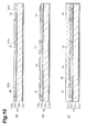
- Fig. 9 to Fig. 14 are sectional side views showing steps of producing the reference element 21 of the infrared detector 1 shown in Fig. 1 .
- a substrate thermally-oxidizing step is performed.
- oxidation is performed on the surface of a Si substrate 100 to form a thermally oxidized film 101 on the Si substrate 100.
- the thermally oxidized film 101 is, for example, 0.7 ⁇ m in film thickness.
- a first-electrode forming step is performed.
- the ROIC pads 26, 27 and the electrode pad 33 of the reference element 21 are formed on the thermally oxidized film 101.
- Al-Si-Ti is laminated at a thickness of 1 ⁇ m, mask processing by photoresist is performed, and thereafter, etching is performed to form the ROIC pads 26, 27 and the electrode pad 33.
- etching dry etching is preferably used for highly uniform formation. Wet etching may also be performed.
- a SiO 2 laminating step is performed.
- a SiO 2 film 102 is laminated on the thermally oxidized film 101, the ROC pads 26, 27 and the electrode pad 33.
- plasma CVD is performed to laminate the SiO 2 film 102 at a thickness of 1 ⁇ m.
- the Si substrate 100, the thermally oxidized film 101 and the SiO 2 film 102 are given as the substrate 100.
- an opening-forming step is performed.
- openings 102a, 102b, 102c are formed on the SiO 2 film 102 respectively at the ROIC pads 26, 27 and the upper part of the electrode pad 33.
- the SiO 2 film 102 is subjected to mask processing with a photoresist and etching is performed to remove the SiO 2 film 102, thereby forming the openings 102a, 102b, 102c.
- a second- electrode forming step is performed.
- a metal layer the material of which is the same as that of the ROIC pads 26, 27 and the electrode pad 33
- mask processing with a photoresist is performed, thereafter, etching is performed to effect patterning, thereby forming the ROIC pads 26, 27, the electrode pad 33 and the metal film 24 for heat dissipation on the side of the substrate.
- the ROIC pads 26, 27 and the electrode pad 33 formed in the first-electrode forming step are respectively integrated with the ROIC pads 26, 27 and the electrode pad 33 formed in the second-electrode forming step.
- a sacrifice-layer coating step is performed.
- the sacrifice layer 36 is formed by coating.
- the sacrifice layer 36 for example, polyimide is used, and the film thickness is, for example, 2.5 ⁇ m.
- a dummy pixel preparing step is performed.
- a protective layer 34 is laminated.
- amorphous silicon is laminated to form the protective layer 34.
- TEOS-SiO 2 SiO 2 film formed by a plasma CVD device using TEOS
- the protective layer 34 for example, lamination at a thickness of 50nm is performed.
- mask processing with a photoresist is formed, and, thereafter, etching is performed to form a plurality of openings 36a which penetrate through the protective layer 34 and the sacrifice layer 36.
- the openings 36a are formed so as to give an inner diameter as small as possible, for example, the inner diameter is 2 ⁇ m.
- An interval pitch of the openings 36a is from 2 ⁇ m to 5 ⁇ m.
- a metal-column forming step is performed.
- a metal film 35 is formed inside the opening 36a and on the upper face of the sacrifice layer 36 formed by the dummy pixel preparing step.
- sputtering is performed to laminate Al, Cu or W at a thickness of 1 ⁇ m, thereby forming the metal film 35.
- metal columns 25 are formed inside the opening 36a.
- the metal columns 25 are, for example, 2 ⁇ m in outer diameter and have a pitch of 2 ⁇ m to 5 ⁇ m.
- the opening 36a is formed so as to be small in inner diameter as much as possible. Therefore, for example, as shown in Fig.
- the metal columns 25 are formed so as to be small in outer diameter, by which a small quantity of metal can be used to reduce material costs.
- a step of forming metal film for heat dissipation is performed.
- mask processing with a photoresist and etching of the metal film 35 are performed, thereby forming a metal film 23 for heat dissipation on the upper part of metal columns 25.
- the metal columns 25 and the metal film 23 for heat dissipation are formed integrally, thus making it possible to disperse stress generated by a difference in thermal expansion between the substrate 10 and the metal columns 25. As a result, it is possible to prevent cracks on the bolometer thin film 15.
- an insulating-film laminating step is performed.
- an insulating film 31 for example, TEOS-SiO 2 is laminated at a thickness of 100nm.
- a bolometer thin film laminating step is performed.
- a bolometer thin film 22 for example, amorphous silicon is laminated at a thickness of 100nm.
- a step of laminating metal film for electrode is performed.
- a metal film for electrode 38 is laminated.
- the metal film for electrode 38 for example, WSi or Ti is laminated at a thickness of 50nm. It is noted that the metal film for electrode 38 may be laminated at a thickness of 100nm.
- an upper-electrode forming step is performed.
- the metal film for electrode 38 is subjected to mask processing with a photoresist and thereafter to patterning, thereby forming an upper electrode 38.
- an opening-forming step is performed.
- openings 39, 40 are formed respectively on the upper layers of the ROIC pads 26, 27.
- openings 41, 42 are formed respectively on a layer of the substrate 10 located between the metal film 24 for heat dissipation on the side of the substrate and the ROIC pads 26, 27, and a layer on the electrode pad 33 is removed.
- an electrode plug forming step is performed.
- sputtering or vacuum deposition is performed to laminate a metal
- lift-off processing is performed to form electrode plugs 28, 29 respectively at the openings 39, 40.
- Al is used to form the electrode plugs 28, 29.
- the upper electrode 38 is integrally formed with the electrode plugs 28, 29 respectively.
- a lower electrode forming step is performed.
- a metal film for electrode is subjected to mask processing with a photoresist, thereafter patterned by lift-off processing, thereby forming a lower electrode 32.
- the lower electrode 32 includes, for example, the ROIC pads 26, 27, the signal processing circuit 14 and a wire connecting therewith.
- a sacrifice-layer removing step is performed.
- a polyimide-made sacrifice layer 36 is subjected to ashing by O 2 .
- the sacrifice layer 36 is completely removed and thermal processing etc., are performed in the process, thus making it possible to prevent unwanted gas generated from the sacrifice layer 36.
- Fig. 9 to Fig. 14 The steps shown in Fig. 9 to Fig. 14 are performed, by which it is possible to produce the reference element 21 capable of dissipating favorably heat resulting from absorption of infrared rays to the substrate 10. It is noted that where the bolometer element 11 is produced, none of the dummy pixel preparing step, the metal column forming step and the step of forming metal film for heat dissipation are needed. Here, the bolometer element 11 and the reference element 21 are able to be produced at the same time on the same substrate 10. In this instance, the bolometer thin film 15 and the bolometer thin film 22 are approximately in parallel with the surface of the substrate 10 and located so as to be approximately flush with each other. Therefore, upon patterning by exposure to light, depth of focus can be controlled easily.
- the infrared detector 1 can be downsized. Further, in the above-described production, the pixel portion 12 and the reference pixel portion 13 are enhanced in uniformity of specific resistance, thus making it possible to enhance functions as a reference element. Then, the signal processing circuit portion 14 produced independently is connected with the pixel portion 12 composed of the bolometer element 11 and the reference pixel portion 13 composed of the reference element 21, thereby completing the infrared detector 1.
- the above-described embodiment shows one example of an infrared detector according to the present invention.
- the infrared detector according to the present invention shall not be limited to the infrared detector according to the embodiment but may include that in which the infrared detector according to the embodiment is modified or applied to others.
- the infrared detector 1 equipped with the reference element 21 having the metal film 24 for heat dissipation on the side of the substrate.
- the reference element 21 is not provided with the metal film 24 for heat dissipation on the side of the substrate.
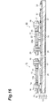
- heat generated at the photodetecting portion 22a by infrared rays is transmitted sequentially from the insulating film 31, the metal film 23 for heat dissipation, to the metal columns 25 and dissipated to the substrate 10. Therefore, as with the above-described embodiment, the reference element 21 detects accurately temperature variation caused by environmental variation etc. It is possible to efficiently reduce the influence of temperature variation in use environment and also achieve downsizing.
- the infrared detector 1 equipped with the bolometer element 11 having the reflection film 20.
- the bolometer element 11 is not provided with the reflection film 20.
- heat generated at the photodetecting portion 22a of the reference element 21 by infrared rays is transmitted sequentially from the insulating film 31, the metal film 23 for heat dissipation, the metal columns 25, to the metal film 24 for heat dissipation on the side of the substrate and dissipated to the substrate 10. Therefore, as with the above-described embodiment, the reference element 21 detects accurately temperature variation caused by environmental variation etc. It is possible to efficiently reduce the influence of temperature variation in use environment and also achieve downsizing.
- the reference element 21 having the metal film 24 for heat dissipation on the side of the substrate, and the infrared detector 1 equipped with the bolometer element 11 having the reflection film 20.
- the reference element 21 is not provided with the metal film 24 for heat dissipation on the side of the substrate and the bolometer element 11 is not provided with the reflection film 20.
- heat generated at the photodetecting portion 22a of the reference element 21 by infrared rays is transmitted sequentially from the insulating film 31, the metal film 23 for heat dissipation to the metal column 25 and dissipated to the substrate 10. Therefore, as with the above-described embodiment, the reference element 21 detects accurately temperature variation caused by environmental variation etc. It is possible to efficiently reduce the influence of temperature variation in use environment and also achieve downsizing.
- the metal columns 25 are formed in a columnar shape. It is also acceptable that the cross section of the metal column 25 is formed in a rectangular or triangular column shape. In this case as well, it is possible to efficiently reduce the influence of temperature variation in use environment and also achieve downsizing.
Landscapes
- Physics & Mathematics (AREA)
- General Physics & Mathematics (AREA)
- Spectroscopy & Molecular Physics (AREA)
- Photometry And Measurement Of Optical Pulse Characteristics (AREA)
- Radiation Pyrometers (AREA)
- Solid State Image Pick-Up Elements (AREA)
- Electromagnetism (AREA)
Abstract
Description
- The present invention relates to a photodetector.
- Conventionally, as a photodetector, there is known a so-called bolometer-type infrared detector for detecting infrared rays by using a material, the resistance value of which varies depending on temperature. As the bolometer-type infrared detector, for example,
Patent Document 1 has disclosed that which is provided with a bolometer element for detecting infrared rays made incident and a reference element for detecting temperature variation caused by variation in use environment, in which signals output by these elements are used to calculate signals excluding the influence of temperature variation caused by variation in use environment, thereby detecting infrared rays. The infrared detector described inPatent Document 1 is provided with a bolometer element having a bolometer thin film supported via a cavity on a silicon substrate which is a thermal capacity body and a reference element having a bolometer thin film formed via a sacrifice layer on the silicon substrate.
Patent Document 1: Japanese Unexamined Patent Application Publication No.10-227689*2 JP10227689A - However, in the infrared detector described in
Patent Document 1, since used is a material small in thermal conductivity and great in thermal capacity as a material for the sacrifice layer of the reference element, there is a fear that the influence of temperature variation in use environment may be insufficiently reduced. - On the other hand, if the sacrifice layer of the reference element is made thin in an attempt to enhance response to temperature variation in use environment, such a constitution is obtained that is greatly different in height between the bolometer element and the reference element. Thus, for example, on patterning by exposure to light, depth of focus is difficult to control and formation of minute patterns is made difficult, which may hinder downsizing of the infrared detector.
- Therefore, the present invention has been made in order to solve the above-described technical problems, an object of which is to provide a photodetector capable of achieving downsizing while sufficiently reducing the influence of temperature variation in use environment.
- More specifically, a photodetector of the present invention is constituted with a first bolometer film which is supported on a surface of a substrate while spaced apart from the surface of the substrate, a second bolometer film which is supported on the surface of the substrate while spaced apart from the surface of the substrate and, a metal film for heat dissipation formed on a surface of the bolometer thin film via an insulating film, wherein the surface of the bolometer thin film faces the substrate, and a plurality of metal columns connected thermally with the first metal film and the substrate.
- In the photodetector of the present invention, via the insulating film, the first metal film and the metal columns, the second bolometer film is connected with the substrate. Therefore, where the second bolometer film is adopted as a bolometer film of the reference element, heat of the second bolometer film generated by infrared rays is efficiently dissipated to the substrate via the insulating film, the first metal film and the metal columns, thus making it possible to measure accurately only the temperature variation caused by variation in use environment. As a result, it is possible to efficiently reduce the influence of temperature variation in use environment. Further, there is no need to make the sacrifice layer thickness thin for efficiently dissipating heat of the reference element to the substrate. Thereby, for example, upon patterning by exposure to light, depth of focus is controlled easily and minute patterning is formed easily, consequently making it possible to achieve downsizing.
- Here, it is preferable that the second metal film is formed at a region facing the second bolometer film on the surface of the substrate and the metal columns are connected with the first metal film and the second metal film.
- Thus, the second metal film is placed between the metal columns and the substrate, thereby where the second bolometer film is adopted as a bolometer film of the reference element, it is possible to increase a thermal contact area of the metal columns with the substrate. Thus, infrared rays made incident can be used to dissipate more efficiently heat generated at the second bolometer film to the substrate.
- Further, it is preferable that at a region facing the first bolometer film on the surface of the substrate, a third metal film is formed. This constitution is obtained, thereby where the first bolometer film is adopted as a bolometer film of the bolometer element, infrared rays transmitted through the first bolometer film are reflected on the first bolometer film by the third metal film and made incident again to the first bolometer film. Therefore, it is possible to efficiently measure heat generated by infrared rays.
- Still further, it is preferable that the first bolometer film and the second bolometer film are located so as to be approximately in parallel with the surface of the substrate and approximately flush with each other. The above constitution is obtained, by which, for example, upon patterning by exposure to light, depth of focus can be controlled more easily.
- According to the present invention, there is provided a photodetector capable of achieving downsizing while efficiently reducing the influence of temperature variation in use environment.
-
-
Fig. 1 is a plan view showing a constitution of an infrared detector which is one embodiment of a photodetector according to the present invention. -
Fig. 2 is a partially enlarged plan view of a pixel portion of the infrared detector ofFig. 1 . -
Fig. 3 is a perspective view of a bolometer element of the pixel portion of the infrared detector ofFig. 1 . -
Fig. 4 is a plan view of the bolometer element of the pixel portion of the infrared detector ofFig. 1 . -
Fig. 5 is a plan view of a reference element at a reference pixel portion of the infrared detector ofFig. 1 . -
Fig. 6 is a combined cross-sectional view taken along line VI - VI ofFig. 4 andFig. 5 . -
Fig. 7 is a circuit diagram of a signal processing circuit portion shown inFig. 1 . -
Fig. 8 is a circuit diagram of the signal processing circuit portion shown inFig. 1 . -
Fig. 9 is a cross sectional view showing a substrate thermally-oxidizing step, a first-electrode forming step and a SiO2 laminating step of the reference element shown inFig. 6 . -
Fig. 10 is a cross sectional view showing an opening-forming step, a second- electrode forming step and a sacrifice-layer coating step of the reference element shown inFig. 6 . -
Fig. 11 is a cross sectional view showing a dummy pixel preparing step, a metal column forming step and a step of forming metal film for heat dissipation of the reference element shown inFig. 6 . -
Fig. 12 is a cross sectional view showing an insulating-film laminating step, a bolometer thin film laminating step and a step of laminating metal film for electrode of the reference element shown inFig. 6 . -
Fig. 13 is a cross sectional view showing an upper-electrode forming step, an opening-forming step and an electrode plug forming step of the reference element shown inFig. 6 . -
Fig. 14 is a cross sectional view showing a lower-electrode forming step and a sacrifice-layer removing step of the reference element shown inFig. 6 . -
Fig. 15 is a schematic diagram for describing effects of metal columns shown inFig. 11 . -
Fig. 16 shows a modified example of the infrared detector shown inFig. 1 . -
Fig. 17 shows a modified example of the infrared detector shown inFig. 1 . -
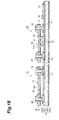
Fig. 18 shows a modified example of the infrared detector shown inFig. 1 . - 1 ... infrared detector (photo detector), 10 ... substrate, 15 ... bolometer thin film (first bolometer thin film), 22 ... bolometer thin film (second bolometer film), 20 ... reflection film (third metal film), 23 ... metal film for heat dissipation (first metal film), 24 ... metal film for heat dissipation on the side of a substrate(second metal film), 25 ... metal column.
- Hereinafter, a description will be made for an embodiment of the present invention by referring to the attached drawings. It is noted that in the descriptions of the drawings, the same reference will be given to the same elements and overlapping description will be omitted.
- A photodetector of the embodiment of the present invention is a so-called bolometer-type infrared detector for detecting infrared rays by the use of a material, the resistance value of which will vary depending on a temperature and favorably used in an infrared imager, thermography etc. First, a description will be made for a constitution of the infrared detector according to the present embodiment.
Fig. 1 is a plan view of an infrared detector which is one embodiment of a photodetector according to the present invention.Fig. 2 is a partially enlarged plan view of a pixel portion of the infrared detector ofFig. 1 .Fig. 3 is a perspective view showing a constitution of one pixel of the infrared detector ofFig. 1 .Fig. 4 is a plan view showing a constitution of one pixel at a pixel portion of the infrared detector ofFig. 1 .Fig. 5 is a plan view showing a constitution of one pixel at a reference pixel portion of the infrared detector given inFig. 1 .Fig. 6 is a schematic cross sectional view of the infrared detector in combination of a cross section taken along line VI - VI ofFig. 4 with that taken along line VI - VI ofFig. 5 . - As shown in
Fig. 1 , aninfrared detector 1 is a detector for detecting infrared rays by thermal variation and constituted with asubstrate 10, apixel portion 12 which is formed on thesubstrate 10 to function as an infrared rays receiving unit, areference pixel portion 13 which is formed on thesubstrate 10 to measure the influence by use environment, and a signalprocessing circuit portion 14. Thepixel portion 12 and thereference pixel portion 13 are respectively connected electrically with the signalprocessing circuit portion 14. As thesubstrate 10, for example, a Si substrate is used. It is noted that hereinafter, where a thermally oxidized layer and a base layer are formed on the surface of the Si substrate, the substrate containing these layers is referred to as thesubstrate 10. - As shown in
Fig. 2 , thepixel portion 12 is formed by arraying two-dimensionally a plurality of pixels (bolometer element 11) on thesubstrate 10 and referred to as a so-called surface micro-machine. Thebolometer element 11 constituting pixels is, as shown inFig. 3 andFig. 4 , provided with ROIC (Read Only IC)pads substrate 10, electrode plugs 18, 19 respectively formed on theROIC pads substrate 10. - The
ROIC pads processing circuit portion 14. The electrode plugs 18, 19 are formed on theROIC pads ROIC pads - The bolometer
thin film 15 is a thin film arranged approximately in parallel with thesubstrate 10 and provided with aphotodetecting portion 15a which receives infrared rays and is formed in a rectangular planar-surface shape, andbeam portions corners photodetecting portion 15a. Thebeam portions corners photodetecting portion 15a and formed so as to face each other. Then, clearances between thephotodetecting portion 15a and thebeam portions slits thin film 15 is made with a material great in specific resistance variation caused by temperature variation, for example, amorphous silicon is used. - Further, at the
beam portions thin film 15,wires photodetecting portion 15a are provided along configurations of thebeam portions Fig. 3 andFig. 6 , the bolometerthin film 15 is supported on the surface of thesubstrate 10 by one-end portions of thebeam portions thin film 15 and thesubstrate 10, there is formed avoid space 11a. Then, as shown inFig. 4 , thewires beam portions wires ROIC pads processing circuit portion 14. - Further, as shown in
Fig. 6 , on a surface of the bolometerthin film 15 facing thesubstrate 10, an insulatingfilm 30 is formed. As the insulatingfilm 30, for example, a silicon-oxidized film is used which is based on TEOS (Tetraethyl orthosilicate) and formed by a plasma CVD (Chemical Vapor Deposition) method. Then, at a region facing the bolometerthin film 15 on the surface of thesubstrate 10 of thebolometer element 11, there is laminated a reflection film (third metal film) 20. As thisreflection film 20, a metal greater in reflectance with respect to infrared rays is used. - Thus, the
bolometer element 11 is constituted in such a manner that the bolometerthin film 15 is apart from the surface of thesubstrate 10 and arranged approximately in parallel with the substrate 10 (membrane constitution), and a clearance between the bolometerthin film 15 and thesubstrate 10 is spatially apart by thevoid space 11a and thermally separated. Then, such a constitution is provided that specific resistance variation caused by temperature variation at thephotodetecting portion 15a of the bolometerthin film 15 is read via thewires ROIC pads processing circuit portion 14. - On the other hand, the
reference pixel portion 13 is formed by arraying two-dimensionally a plurality of pixels (reference element 21) on thesubstrate 10, and each of the pixels is given as a so-called optical black. The pixel-constitutingreference element 21 is, as shown inFig. 5 andFig. 6 , constituted so as to be substantially similar to thebolometer element 11, but different from thebolometer element 11 in that it is provided with a metal film for heat dissipation (first metal film) 23, a metal film for heat dissipation on the side of a substrate (second metal film) 24 and a plurality ofmetal columns 25. It is noted that a description will be omitted for theROIC pads bolometer element 11. - The bolometer thin film (second bolometer film) 22 has a similar constitution to the bolometer
thin film 15 and is provided with aphotodetecting portion 22a,beam portions wires Fig. 6 , the bolometerthin film 22 and the bolometerthin film 15 are approximately in parallel with the surface of thesubstrate 10 and located so as to be approximately flush with each other. Here, being approximately flush means a planar surface in such a range that includes a difference in thickness of ametal film 23 for heat dissipation to be described later in a laminating direction, for example, a planar surface within a range of approximately ±1 µm. - Further, on a surface of the
photodetecting portion 22a facing thesubstrate 10, there is formed a rectangular planar surface-shapedmetal film 23 for heat dissipation via an insulatingfilm 31. The insulatingfilm 31 is constituted with a material similar to that of the insulatingfilm 30 of thebolometer element 11. Still further, as themetal film 23 for heat dissipation, for example, Al, Cu or W is used. - Then, between the
metal film 23 for heat dissipation and thesubstrate 10 there are formed a plurality ofmetal columns 25. Themetal columns 25 which are columns made with a metal and extending in a laminating direction are formed apart at constant intervals in a direction orthogonal to the laminating direction. Themetal columns 25 are thermally connected with themetal film 23 for heat dissipation and thesubstrate 10. As themetal columns 25, for example, Al, Cu or W is used. It is noted that themetal columns 25 may be formed integrally with themetal film 23 for heat dissipation. Further, at a region facing thephotodetecting portion 22a of the bolometerthin film 22, on a surface of thereference element 21 facing thesubstrate 10, there is formed a rectangular planar surface-shapedmetal film 24 for heat dissipation on the side of the substrate. Themetal film 24 for heat dissipation on the side of the substrate has an area greater than a cross-sectional area of the plurality ofmetal columns 25 and thermally connected with themetal columns 25 and thesubstrate 10. Themetal film 24 for heat dissipation on the side of the substrate is made with a metal and, for example, Al, Cu or W is used. - As described so far, the
reference element 21 is constituted in such a manner that heat generated by temperature variation caused at the bolometerthin film 22 by infrared rays made incident is dissipated to thesubstrate 10 via the insulatingfilm 31, themetal film 23 for heat dissipation, themetal columns 25, and themetal film 24 for heat dissipation on the side of the substrate. Then, such a constitution is provided that specific resistance variation caused by temperature variation such as environmental variation of the bolometerthin film 22 etc., can be read via thewires ROIC pads processing circuit portion 14. - Further, the signal
processing circuit portion 14 shown inFig. 1 is a reading-out circuit which is installed on thesubstrate 10, and has functions to read out output signals of thepixel portion 12 and thereference pixel portion 13 to subtract the output signal of thereference pixel portion 13 from output signal of thepixel portion 12. Hereinafter, the reading-out circuit will be specifically described by referring toFig. 7 andFig. 8 .Fig. 7 andFig. 8 are circuit diagrams showing reading-out circuits at the signalprocessing circuit portion 14. First, with easy understanding of the description taken into account, a description will be made by exemplifying a minimally constituted infrared detector having respectively onebolometer element 11 and onereference element 21. In this minimum constitution, for example, an integrating circuit shown inFig. 7 is used to measure an output voltage Vout. The output voltage Vout is expressed in the following formula (1) by giving a charge amplifier input current obtained by subtracting a reference resistance current I (Rref) flowing to thephotodetecting portion 22a of thereference element 21 from a bolometer current I (Rb) flowing to thephotodetecting portion 15a of thebolometer element 11 as Ip and giving an integral capacity of a condenser as Cf,
- The signal
processing circuit portion 14 uses the formula (1) to convert variation in resistance value to variation in output voltage Vout, thereby detecting infrared rays on the basis of this electric signal. Next, a description will be made for an infrared detector made up of a plurality ofbolometer elements 11 and onereference element 21. In this instance, for example, as shown in the circuit diagram ofFig. 8 , a shift register SR is used to measure an output voltage Vout on the basis of a charge amplifier input current Ip corresponding to each bolometer current I (Rbn) (n: an integral). Then, on the basis of this electrical signal, infrared rays are detected. - Next, a description will be made for operations of the above-constituted
infrared detector 1. First, when infrared rays are made incident into theinfrared detector 1, infrared rays are absorbed at thephotodetecting portion 15a of thebolometer element 11 and converted to heat. Here, thephotodetecting portion 15a is thermally separated by avoid space 11a formed between theslits thin film 15 and thesubstrate 10. Therefore, heat generated at thephotodetecting portion 15a is not dissipated around but elevating a temperature at thephotodetecting portion 15a to vary a resistance value of thephotodetecting portion 15a according to the temperature elevation. Thus, variation in resistance value is sent as a signal via thewires photodetecting portion 15a, electrode plugs 18, 19 and theROIC pads processing circuit portion 14. - Further, where some of the infrared rays which have been made incident into the bolometer
thin film 15 are not absorbed at thephotodetecting portion 15a but transmitted, the thus transmitted infrared rays are reflected by thereflection film 20 and made incident again into thephotodetecting portion 15a. The infrared rays made incident again are absorbed at thephotodetecting portion 15a and converted to heat. Thereby, it is possible to efficiently absorb infrared rays. - On the other hand, when infrared rays are made incident into the
infrared detector 1, as with thebolometer element 11, infrared rays are made incident into thereference element 21 as well, and the infrared rays are absorbed at thephotodetecting portion 22a of thereference element 21 and converted to heat. Here, thephotodetecting portion 22a is thermally connected via the insulatingfilm 31 with themetal film 23 for heat dissipation, themetal columns 25, themetal film 24 for heat dissipation on the side of the substrate, and thesubstrate 10. Therefore, heat generated at thephotodetecting portion 15a by infrared rays which have been made incident is transmitted sequentially from the insulatingfilm 31, themetal film 23 for heat dissipation, themetal columns 25 to themetal film 24 for heat dissipation on the side of the substrate and dissipated to thesubstrate 10. Therefore, only heat generated by temperature variation caused by environmental variation of theinfrared detector 1 will vary a resistance value of thephotodetecting portion 22a. Thus, variation in resistance value caused by the environmental variation will be sent to the signalprocessing circuit portion 14 as a signal via thewires photodetecting portion 22a, the electrode plugs 28, 29 and theROIC pads - Then, at the signal
processing circuit portion 14, variation in resistance value of thephotodetecting portions - Thus, in the
infrared detector 1, the bolometerthin film 22 is connected with thesubstrate 10 via the insulatingfilm 31, themetal film 23 for heat dissipation and themetal columns 25 at thereference element 21. Therefore, heat generated by infrared rays at thephotodetecting portion 22a of the bolometerthin film 22 is efficiently dissipated to thesubstrate 10 via the insulatingfilm 31, themetal film 23 for heat dissipation, a plurality ofmetal columns 25, themetal film 24 for heat dissipation on the side of the substrate, thus making it possible to accurately measure only temperature variation caused by variation in use environment. As a result, it is possible to efficiently reduce the influence of temperature variation in use environment. - Further, in the
reference element 21, themetal film 24 for heat dissipation on the side of the substrate is placed between themetal columns 25 and thesubstrate 10, thus making it possible to increase a thermal contact area of themetal columns 25 and thesubstrate 10. Thereby, it is possible to dissipate more efficiently heat generated at the bolometerthin film 22 by the infrared rays made incident to thesubstrate 10. - Further, in the
reference element 21, a member thermally connecting thephotodetecting portion 22a and thesubstrate 10 is constituted with a plurality ofcolumnar metal columns 25. Therefore, as compared with a case where a member thermally connecting thephotodetecting portion 22a and thesubstrate 10 being constituted with a mass of metal, a difference in thermal expansion between thephotodetecting portion 22a and themetal columns 25 or between thesubstrate 10 and themetal columns 25 can be used to prevent stress from being applied to the bolometerthin film 15. As a result, it is possible to prevent cracks on the bolometerthin film 15. - Still further, in the
reference element 21, where themetal columns 25 are formed integrally with themetal film 23 for heat dissipation, it is possible to disperse stress caused by a difference in thermal expansion between thesubstrate 10 and a heat transmitting body. As a result, it is possible to prevent cracks on the bolometerthin film 15. - In addition, since the
reference element 21 is similar in configuration to thebolometer element 11, it is possible to reduce a resistance difference resulting from a difference in configuration between the elements. This is favorably adoptable as a reference element. - Next, a description will be made for a method for producing the
infrared detector 1 according to the present embodiment. It is noted that steps of producing thereference element 21 include a step of producing thebolometer element 11. Therefore, hereinafter, a description will be made mainly for steps of producing thereference element 21.Fig. 9 to Fig. 14 are sectional side views showing steps of producing thereference element 21 of theinfrared detector 1 shown inFig. 1 . - First, as shown in
Fig. 9(a) , a substrate thermally-oxidizing step is performed. In this step, oxidation is performed on the surface of aSi substrate 100 to form a thermally oxidizedfilm 101 on theSi substrate 100. The thermally oxidizedfilm 101 is, for example, 0.7µm in film thickness. - Next, as shown in
Fig. 9(b) , a first-electrode forming step is performed. In this step, theROIC pads electrode pad 33 of thereference element 21 are formed on the thermally oxidizedfilm 101. For example, Al-Si-Ti is laminated at a thickness of 1µm, mask processing by photoresist is performed, and thereafter, etching is performed to form theROIC pads electrode pad 33. As etching, dry etching is preferably used for highly uniform formation. Wet etching may also be performed. - Then, as shown in
Fig. 9 (c) , a SiO2 laminating step is performed. In this step, a SiO2 film 102 is laminated on the thermally oxidizedfilm 101, theROC pads electrode pad 33. For example, plasma CVD is performed to laminate the SiO2 film 102 at a thickness of 1µm. It is noted that, here, theSi substrate 100, the thermally oxidizedfilm 101 and the SiO2 film 102 are given as thesubstrate 100. - Then, as shown in
Fig. 10 (d) , an opening-forming step is performed. In this step,openings ROIC pads electrode pad 33. For example, the SiO2 film 102 is subjected to mask processing with a photoresist and etching is performed to remove the SiO2 film 102, thereby forming theopenings - Next, as shown in
Fig. 10(e) , a second- electrode forming step is performed. In this step, there is formed a metal layer, the material of which is the same as that of theROIC pads electrode pad 33, mask processing with a photoresist is performed, thereafter, etching is performed to effect patterning, thereby forming theROIC pads electrode pad 33 and themetal film 24 for heat dissipation on the side of the substrate. More specifically, theROIC pads electrode pad 33 formed in the first-electrode forming step are respectively integrated with theROIC pads electrode pad 33 formed in the second-electrode forming step. Upper faces of theROIC pads electrode pad 33 are formed so as to be located on the SiO2 film 102 via theopening ROIC pads electrode pad 33 and themetal film 24 for heat dissipation on the side of the substrate are formed so that they are located to be flush with each other. Thus, the upper faces of theROIC pads electrode pad 33 and themetal film 24 for heat dissipation on the side of the substrate are formed so that they are located to be flush with each other, by which a membrane structure of thereference element 21 is planarized. - Then, as shown in
Fig. 10(f) , a sacrifice-layer coating step is performed. In this step, thesacrifice layer 36 is formed by coating. As thesacrifice layer 36, for example, polyimide is used, and the film thickness is, for example, 2.5µm. - Next, as shown in
Fig. 11(g) , a dummy pixel preparing step is performed. In this step, first, as prior processing for forming an opening, aprotective layer 34 is laminated. For example, amorphous silicon is laminated to form theprotective layer 34. Further, TEOS-SiO2 (SiO2 film formed by a plasma CVD device using TEOS) may be laminated to form theprotective layer 34. As theprotective layer 34, for example, lamination at a thickness of 50nm is performed. Then, mask processing with a photoresist is formed, and, thereafter, etching is performed to form a plurality ofopenings 36a which penetrate through theprotective layer 34 and thesacrifice layer 36. Theopenings 36a are formed so as to give an inner diameter as small as possible, for example, the inner diameter is 2µm. An interval pitch of theopenings 36a is from 2µm to 5µm. Then, after formation of theopenings 36a, thesacrifice layer 36 is removed. Where, as thesacrifice layer 36, for example, amorphous silicon is used, XeF2 is used for removing the layer. Where, as thesacrifice layer 36, for example, TEOS-SiO2 is used, HF is used for removing the layer. - Then, as shown in
Fig. 11(h) , a metal-column forming step is performed. In this step, ametal film 35 is formed inside theopening 36a and on the upper face of thesacrifice layer 36 formed by the dummy pixel preparing step. For example, sputtering is performed to laminate Al, Cu or W at a thickness of 1µm, thereby forming themetal film 35. Thereby,metal columns 25 are formed inside theopening 36a. Themetal columns 25 are, for example, 2µm in outer diameter and have a pitch of 2µm to 5µm. Here, in the dummy pixel preparing step, theopening 36a is formed so as to be small in inner diameter as much as possible. Therefore, for example, as shown inFig. 15(a) , as compared with a case where the outer diameter of the metal column 25 (more specifically, the inner diameter of theopening 36a) is great, as shown inFig. 15(b) , it is possible to planarize themetal film 35 continuing to the upper part of themetal column 25. Thereby, such a necessity is eliminated that in order to planarize a membrane structure, a planarization step (etch-back step) is performed after the metal column forming step, thus making it possible to reduce production costs. Further, themetal columns 25 are formed so as to be small in outer diameter, by which a small quantity of metal can be used to reduce material costs. - Then, as shown in
Fig. 11(i) , a step of forming metal film for heat dissipation is performed. In this step, mask processing with a photoresist and etching of themetal film 35 are performed, thereby forming ametal film 23 for heat dissipation on the upper part ofmetal columns 25. Thus, themetal columns 25 and themetal film 23 for heat dissipation are formed integrally, thus making it possible to disperse stress generated by a difference in thermal expansion between thesubstrate 10 and themetal columns 25. As a result, it is possible to prevent cracks on the bolometerthin film 15. - Then, as shown in
Fig. 12(j) , an insulating-film laminating step is performed. In this step, as an insulatingfilm 31, for example, TEOS-SiO2 is laminated at a thickness of 100nm. Thereafter, as shown inFig. 12(k) , a bolometer thin film laminating step is performed. In this step, as a bolometerthin film 22, for example, amorphous silicon is laminated at a thickness of 100nm. Thereafter, as shown inFig. 12(l) , a step of laminating metal film for electrode is performed. In this step, a metal film forelectrode 38 is laminated. As the metal film forelectrode 38, for example, WSi or Ti is laminated at a thickness of 50nm. It is noted that the metal film forelectrode 38 may be laminated at a thickness of 100nm. - Next, as shown in
Fig. 13(m) , an upper-electrode forming step is performed. In this step, the metal film forelectrode 38 is subjected to mask processing with a photoresist and thereafter to patterning, thereby forming anupper electrode 38. Thereafter, as shown inFig. 13(n) , an opening-forming step is performed. In this step,openings ROIC pads openings substrate 10 located between themetal film 24 for heat dissipation on the side of the substrate and theROIC pads electrode pad 33 is removed. - Then, as shown in
Fig. 13(o) , an electrode plug forming step is performed. In this step, sputtering or vacuum deposition is performed to laminate a metal, thereafter, lift-off processing is performed to form electrode plugs 28, 29 respectively at theopenings upper electrode 38 is integrally formed with the electrode plugs 28, 29 respectively. - Next, as shown in
Fig. 14(p) , a lower electrode forming step is performed. In this step, a metal film for electrode is subjected to mask processing with a photoresist, thereafter patterned by lift-off processing, thereby forming alower electrode 32. Thelower electrode 32 includes, for example, theROIC pads signal processing circuit 14 and a wire connecting therewith. Thereafter, as shown inFig. 14(q) , a sacrifice-layer removing step is performed. In this step, for example, a polyimide-madesacrifice layer 36 is subjected to ashing by O2. Thus, thesacrifice layer 36 is completely removed and thermal processing etc., are performed in the process, thus making it possible to prevent unwanted gas generated from thesacrifice layer 36. - The steps shown in
Fig. 9 to Fig. 14 are performed, by which it is possible to produce thereference element 21 capable of dissipating favorably heat resulting from absorption of infrared rays to thesubstrate 10. It is noted that where thebolometer element 11 is produced, none of the dummy pixel preparing step, the metal column forming step and the step of forming metal film for heat dissipation are needed. Here, thebolometer element 11 and thereference element 21 are able to be produced at the same time on thesame substrate 10. In this instance, the bolometerthin film 15 and the bolometerthin film 22 are approximately in parallel with the surface of thesubstrate 10 and located so as to be approximately flush with each other. Therefore, upon patterning by exposure to light, depth of focus can be controlled easily. As a result, theinfrared detector 1 can be downsized. Further, in the above-described production, thepixel portion 12 and thereference pixel portion 13 are enhanced in uniformity of specific resistance, thus making it possible to enhance functions as a reference element. Then, the signalprocessing circuit portion 14 produced independently is connected with thepixel portion 12 composed of thebolometer element 11 and thereference pixel portion 13 composed of thereference element 21, thereby completing theinfrared detector 1. - It is noted that the above-described embodiment shows one example of an infrared detector according to the present invention. The infrared detector according to the present invention shall not be limited to the infrared detector according to the embodiment but may include that in which the infrared detector according to the embodiment is modified or applied to others.
- For example, in the above-described embodiment, a description has been made for the
infrared detector 1 equipped with thereference element 21 having themetal film 24 for heat dissipation on the side of the substrate. However, as shown inFig. 16 , also acceptable is that in which thereference element 21 is not provided with themetal film 24 for heat dissipation on the side of the substrate. In the above constitution, heat generated at thephotodetecting portion 22a by infrared rays is transmitted sequentially from the insulatingfilm 31, themetal film 23 for heat dissipation, to themetal columns 25 and dissipated to thesubstrate 10. Therefore, as with the above-described embodiment, thereference element 21 detects accurately temperature variation caused by environmental variation etc. It is possible to efficiently reduce the influence of temperature variation in use environment and also achieve downsizing. - Further, in the above-described embodiment, a description has been made for the
infrared detector 1 equipped with thebolometer element 11 having thereflection film 20. However, as shown inFig. 17 , also acceptable is that in which thebolometer element 11 is not provided with thereflection film 20. In the above constitution as well, heat generated at thephotodetecting portion 22a of thereference element 21 by infrared rays is transmitted sequentially from the insulatingfilm 31, themetal film 23 for heat dissipation, themetal columns 25, to themetal film 24 for heat dissipation on the side of the substrate and dissipated to thesubstrate 10. Therefore, as with the above-described embodiment, thereference element 21 detects accurately temperature variation caused by environmental variation etc. It is possible to efficiently reduce the influence of temperature variation in use environment and also achieve downsizing. - Still further, in the above-described embodiment, a description has been made for the
reference element 21 having themetal film 24 for heat dissipation on the side of the substrate, and theinfrared detector 1 equipped with thebolometer element 11 having thereflection film 20. However, as shown inFig. 18 , also acceptable is that in which thereference element 21 is not provided with themetal film 24 for heat dissipation on the side of the substrate and thebolometer element 11 is not provided with thereflection film 20. In the above constitution, heat generated at thephotodetecting portion 22a of thereference element 21 by infrared rays is transmitted sequentially from the insulatingfilm 31, themetal film 23 for heat dissipation to themetal column 25 and dissipated to thesubstrate 10. Therefore, as with the above-described embodiment, thereference element 21 detects accurately temperature variation caused by environmental variation etc. It is possible to efficiently reduce the influence of temperature variation in use environment and also achieve downsizing. - In addition, in the above-described embodiment, a description has been made for a case where the
metal columns 25 are formed in a columnar shape. It is also acceptable that the cross section of themetal column 25 is formed in a rectangular or triangular column shape. In this case as well, it is possible to efficiently reduce the influence of temperature variation in use environment and also achieve downsizing.
Claims (4)
- A photodetector comprising:a first bolometer film supported on a surface of a substrate while spaced apart from the surface of the substrate;a second bolometer film supported on the surface of the substrate while spaced apart from the surface of the substrate and;a first metal film formed on a surface of the second bolometer film via an insulating film, wherein the surface of the second bolometer film faces the substrate, anda plurality of metal columns thermally connected with the first metal film and the substrate.
- The photodetector according to claim 1, wherein at a region facing the second bolometer film on the surface of the substrate, a second metal film is formed and the metal columns are connected with the first metal film and the second metal film.
- The photodetector according to claim 1, wherein at a region facing the first bolometer film on the surface of the substrate, a third metal film is formed.
- The photodetector according to claim 1, wherein the first bolometer film and the second bolometer film are approximately in parallel with the surface of the substrate and located so as to be approximately flush with each other.
Applications Claiming Priority (2)
| Application Number | Priority Date | Filing Date | Title |
|---|---|---|---|
| JP2008068074A JP5255873B2 (en) | 2008-03-17 | 2008-03-17 | Photodetector |
| PCT/JP2009/055064 WO2009116496A1 (en) | 2008-03-17 | 2009-03-16 | Photodetector |
Publications (3)
| Publication Number | Publication Date |
|---|---|
| EP2261617A1 true EP2261617A1 (en) | 2010-12-15 |
| EP2261617A4 EP2261617A4 (en) | 2012-05-02 |
| EP2261617B1 EP2261617B1 (en) | 2014-07-16 |
Family
ID=41090897
Family Applications (1)
| Application Number | Title | Priority Date | Filing Date |
|---|---|---|---|
| EP09723540.2A Not-in-force EP2261617B1 (en) | 2008-03-17 | 2009-03-16 | Photodetector |
Country Status (7)
| Country | Link |
|---|---|
| US (1) | US8692348B2 (en) |
| EP (1) | EP2261617B1 (en) |
| JP (1) | JP5255873B2 (en) |
| KR (2) | KR101708608B1 (en) |
| CN (1) | CN101978246B (en) |
| TW (1) | TWI457547B (en) |
| WO (1) | WO2009116496A1 (en) |
Cited By (2)
| Publication number | Priority date | Publication date | Assignee | Title |
|---|---|---|---|---|
| CN103459994A (en) * | 2011-03-25 | 2013-12-18 | 浜松光子学株式会社 | Infrared image sensor and signal readout method |
| EP3260827A4 (en) * | 2015-02-18 | 2018-10-24 | Hamamatsu Photonics K.K. | Infrared detection device |
Families Citing this family (9)
| Publication number | Priority date | Publication date | Assignee | Title |
|---|---|---|---|---|
| JP5259430B2 (en) * | 2009-01-06 | 2013-08-07 | 浜松ホトニクス株式会社 | Photodetector |
| KR101922119B1 (en) | 2011-12-22 | 2019-02-14 | 삼성전자주식회사 | Infrared detector and method for detecting infrared using the same |
| US9297700B2 (en) | 2012-12-03 | 2016-03-29 | Analog Devices, Inc. | Photonic sensor and a method of manufacturing such a sensor |
| FR3009865B1 (en) * | 2013-08-22 | 2015-07-31 | Commissariat Energie Atomique | BOLOMETRIC DETECTOR WITH REINFORCED THERMALIZATION COMPENSATION BOLOMETER |
| WO2016020993A1 (en) * | 2014-08-06 | 2016-02-11 | 株式会社日立製作所 | Infrared sensor and signal detection method |
| FR3048125B1 (en) * | 2016-02-24 | 2020-06-05 | Commissariat A L'energie Atomique Et Aux Energies Alternatives | ELECTROMAGNETIC RADIATION DETECTION DEVICE WITH RAISED ELECTRICAL CONNECTION PLOT |
| JP2022025052A (en) * | 2020-07-28 | 2022-02-09 | 日本電気株式会社 | Bolometer and manufacturing method therefor |
| TWI902642B (en) * | 2023-05-31 | 2025-10-21 | 松翰科技股份有限公司 | Manufacturing method of micro-bolometer |
| TWI902641B (en) * | 2023-05-31 | 2025-10-21 | 松翰科技股份有限公司 | Manufacturing method of micro-bolometer |
Family Cites Families (22)
| Publication number | Priority date | Publication date | Assignee | Title |
|---|---|---|---|---|
| JPH04274346A (en) * | 1991-02-28 | 1992-09-30 | Mitsubishi Electric Corp | Semiconductor device |
| JPH06326367A (en) | 1993-05-13 | 1994-11-25 | Fujitsu Ltd | Infrared detector and manufacturing method thereof |
| JP2655101B2 (en) | 1994-10-28 | 1997-09-17 | 日本電気株式会社 | Infrared sensor |
| JPH10185681A (en) * | 1996-11-08 | 1998-07-14 | Mitsuteru Kimura | Thermal infrared sensor, method of manufacturing the same, and infrared image sensor using the same |
| JP3040356B2 (en) * | 1997-01-27 | 2000-05-15 | 三菱電機株式会社 | Infrared solid-state imaging device |
| JPH10227689A (en) | 1997-02-17 | 1998-08-25 | Mitsubishi Electric Corp | Infrared detector and infrared focal plane array |
| CN1177204C (en) * | 1998-12-18 | 2004-11-24 | 株式会社大宇电子 | Structurally stable infrared bolometer |
| JP3866040B2 (en) * | 1998-12-18 | 2007-01-10 | デーウー・エレクトロニクス・コーポレイション | Structurally stable infrared bolometer |
| JP3460810B2 (en) * | 1999-07-26 | 2003-10-27 | 日本電気株式会社 | Thermal infrared detector with thermal separation structure |
| JP2001041818A (en) | 1999-07-27 | 2001-02-16 | Sharp Corp | Bolometer type infrared detecting element and infrared image sensor using the same |
| US6690014B1 (en) | 2000-04-25 | 2004-02-10 | Raytheon Company | Microbolometer and method for forming |
| JP2002107224A (en) * | 2000-09-29 | 2002-04-10 | Toshiba Corp | Infrared sensor and method of manufacturing the same |
| JP4135857B2 (en) * | 2001-03-27 | 2008-08-20 | 独立行政法人産業技術総合研究所 | Infrared sensor manufacturing method |
| JP2005043381A (en) * | 2004-10-18 | 2005-02-17 | Nec Corp | Thermal infrared detector and method for manufacturing the same |
| WO2006108210A1 (en) * | 2005-02-25 | 2006-10-19 | Kevin Liddiard | Microbolometer infrared security sensor |
| EP1880176B1 (en) * | 2005-05-12 | 2010-02-17 | Commissariat à l'Energie Atomique | Thermal detector for electromagnetic radiation and infrared detection device using said detectors |
| US7385199B2 (en) * | 2005-09-26 | 2008-06-10 | Teledyne Licensing, Llc | Microbolometer IR focal plane array (FPA) with in-situ mirco vacuum sensor and method of fabrication |
| JP2008022315A (en) * | 2006-07-13 | 2008-01-31 | Mitsubishi Electric Corp | Thermal infrared detection circuit |
| US20080135758A1 (en) * | 2006-12-06 | 2008-06-12 | Electronics And Telecommunications Research Institute | Bolometer and method of manufacturing the same |
| JP2008219613A (en) * | 2007-03-06 | 2008-09-18 | Mitsubishi Electric Corp | Uncooled infrared camera |
| KR100925214B1 (en) | 2007-11-29 | 2009-11-06 | 한국전자통신연구원 | Volometer and its manufacturing method |
| US8523427B2 (en) * | 2008-02-27 | 2013-09-03 | Analog Devices, Inc. | Sensor device with improved sensitivity to temperature variation in a semiconductor substrate |
-
2008
- 2008-03-17 JP JP2008068074A patent/JP5255873B2/en not_active Expired - Fee Related
-
2009
- 2009-03-16 US US12/922,805 patent/US8692348B2/en not_active Expired - Fee Related
- 2009-03-16 KR KR1020167033698A patent/KR101708608B1/en not_active Expired - Fee Related
- 2009-03-16 CN CN200980109704.XA patent/CN101978246B/en not_active Expired - Fee Related
- 2009-03-16 EP EP09723540.2A patent/EP2261617B1/en not_active Not-in-force
- 2009-03-16 WO PCT/JP2009/055064 patent/WO2009116496A1/en not_active Ceased
- 2009-03-16 KR KR1020107018149A patent/KR101683257B1/en not_active Expired - Fee Related
- 2009-03-17 TW TW098108637A patent/TWI457547B/en not_active IP Right Cessation
Cited By (6)
| Publication number | Priority date | Publication date | Assignee | Title |
|---|---|---|---|---|
| CN103459994A (en) * | 2011-03-25 | 2013-12-18 | 浜松光子学株式会社 | Infrared image sensor and signal readout method |
| EP2690416A4 (en) * | 2011-03-25 | 2014-09-10 | Hamamatsu Photonics Kk | INFRARED IMAGE SENSOR AND METHOD FOR READING SIGNALS |
| US9253418B2 (en) | 2011-03-25 | 2016-02-02 | Hamamatsu Photonics K.K. | Infrared image sensor and signal read method |
| CN103459994B (en) * | 2011-03-25 | 2016-11-09 | 浜松光子学株式会社 | Infrared image sensor and signal readout method |
| EP3260827A4 (en) * | 2015-02-18 | 2018-10-24 | Hamamatsu Photonics K.K. | Infrared detection device |
| US10480995B2 (en) | 2015-02-18 | 2019-11-19 | Hamamatsu Photonics K.K. | Infrared detection device |
Also Published As
| Publication number | Publication date |
|---|---|
| US8692348B2 (en) | 2014-04-08 |
| TW201005270A (en) | 2010-02-01 |
| JP2009222585A (en) | 2009-10-01 |
| EP2261617B1 (en) | 2014-07-16 |
| KR20160143876A (en) | 2016-12-14 |
| KR101708608B1 (en) | 2017-02-20 |
| US20110024855A1 (en) | 2011-02-03 |
| KR20100133363A (en) | 2010-12-21 |
| WO2009116496A1 (en) | 2009-09-24 |
| CN101978246B (en) | 2014-07-09 |
| TWI457547B (en) | 2014-10-21 |
| JP5255873B2 (en) | 2013-08-07 |
| KR101683257B1 (en) | 2016-12-06 |
| EP2261617A4 (en) | 2012-05-02 |
| CN101978246A (en) | 2011-02-16 |
Similar Documents
| Publication | Publication Date | Title |
|---|---|---|
| EP2261617B1 (en) | Photodetector | |
| JP5259430B2 (en) | Photodetector | |
| US6552344B1 (en) | Infrared detector and method of making the infrared detector | |
| US8734010B2 (en) | Thermal detector, thermal detection device, electronic instrument, and thermal detector manufacturing method | |
| JP7019347B2 (en) | Imaging device | |
| US8569698B2 (en) | Thermal detector, thermal detection device, and electronic instrument | |
| KR20180123638A (en) | Method For Producing A Bolometric Detector | |
| JP2003329515A (en) | Bolometer type infrared solid-state image sensor | |
| JP4496751B2 (en) | Thermal infrared solid-state imaging device and manufacturing method thereof | |
| JP2006300623A (en) | Infrared sensor | |
| JP2008039570A (en) | Thermal infrared solid-state imaging device and infrared camera | |
| US20150122999A1 (en) | Thermal detector, thermal detection device, electronic instrument, and thermal detector manufacturing method | |
| JP2010101675A (en) | Infrared imaging element and method of manufacturing the same | |
| JP2000346704A (en) | Bolometer type infrared detector | |
| JP2004271386A (en) | Thermal infrared detector and its manufacturing method | |
| JP2010045095A (en) | Infrared imaging element and its manufacturing method | |
| GB2513170A (en) | A detection system and a method of making a detection system |
Legal Events
| Date | Code | Title | Description |
|---|---|---|---|
| PUAI | Public reference made under article 153(3) epc to a published international application that has entered the european phase |
Free format text: ORIGINAL CODE: 0009012 |
|
| 17P | Request for examination filed |
Effective date: 20101014 |
|
| AK | Designated contracting states |
Kind code of ref document: A1 Designated state(s): AT BE BG CH CY CZ DE DK EE ES FI FR GB GR HR HU IE IS IT LI LT LU LV MC MK MT NL NO PL PT RO SE SI SK TR |
|
| AX | Request for extension of the european patent |
Extension state: AL BA RS |
|
| DAX | Request for extension of the european patent (deleted) | ||
| A4 | Supplementary search report drawn up and despatched |
Effective date: 20120402 |
|
| RIC1 | Information provided on ipc code assigned before grant |
Ipc: H01L 27/144 20060101ALI20120327BHEP Ipc: G01J 1/02 20060101AFI20120327BHEP Ipc: H01L 37/00 20060101ALI20120327BHEP Ipc: G01J 1/42 20060101ALI20120327BHEP Ipc: H01L 27/146 20060101ALI20120327BHEP |
|
| RIC1 | Information provided on ipc code assigned before grant |
Ipc: G01J 1/02 20060101AFI20130806BHEP Ipc: G01J 1/42 20060101ALI20130806BHEP Ipc: H01L 27/144 20060101ALI20130806BHEP Ipc: H01L 27/146 20060101ALI20130806BHEP Ipc: G01J 5/20 20060101ALI20130806BHEP Ipc: H01L 37/00 20060101ALI20130806BHEP |
|
| GRAP | Despatch of communication of intention to grant a patent |
Free format text: ORIGINAL CODE: EPIDOSNIGR1 |
|
| INTG | Intention to grant announced |
Effective date: 20131018 |
|
| GRAP | Despatch of communication of intention to grant a patent |
Free format text: ORIGINAL CODE: EPIDOSNIGR1 |
|
| INTG | Intention to grant announced |
Effective date: 20140221 |
|
| GRAS | Grant fee paid |
Free format text: ORIGINAL CODE: EPIDOSNIGR3 |
|
| GRAA | (expected) grant |
Free format text: ORIGINAL CODE: 0009210 |
|
| AK | Designated contracting states |
Kind code of ref document: B1 Designated state(s): AT BE BG CH CY CZ DE DK EE ES FI FR GB GR HR HU IE IS IT LI LT LU LV MC MK MT NL NO PL PT RO SE SI SK TR |
|
| REG | Reference to a national code |
Ref country code: GB Ref legal event code: FG4D |
|
| REG | Reference to a national code |
Ref country code: CH Ref legal event code: EP |
|
| REG | Reference to a national code |
Ref country code: IE Ref legal event code: FG4D |
|
| REG | Reference to a national code |
Ref country code: AT Ref legal event code: REF Ref document number: 677918 Country of ref document: AT Kind code of ref document: T Effective date: 20140815 |
|
| REG | Reference to a national code |
Ref country code: DE Ref legal event code: R096 Ref document number: 602009025319 Country of ref document: DE Effective date: 20140828 |
|
| REG | Reference to a national code |
Ref country code: NL Ref legal event code: VDEP Effective date: 20140716 |
|
| REG | Reference to a national code |
Ref country code: AT Ref legal event code: MK05 Ref document number: 677918 Country of ref document: AT Kind code of ref document: T Effective date: 20140716 |
|
| REG | Reference to a national code |
Ref country code: LT Ref legal event code: MG4D |
|
| PG25 | Lapsed in a contracting state [announced via postgrant information from national office to epo] |
Ref country code: GR Free format text: LAPSE BECAUSE OF FAILURE TO SUBMIT A TRANSLATION OF THE DESCRIPTION OR TO PAY THE FEE WITHIN THE PRESCRIBED TIME-LIMIT Effective date: 20141017 Ref country code: SE Free format text: LAPSE BECAUSE OF FAILURE TO SUBMIT A TRANSLATION OF THE DESCRIPTION OR TO PAY THE FEE WITHIN THE PRESCRIBED TIME-LIMIT Effective date: 20140716 Ref country code: BG Free format text: LAPSE BECAUSE OF FAILURE TO SUBMIT A TRANSLATION OF THE DESCRIPTION OR TO PAY THE FEE WITHIN THE PRESCRIBED TIME-LIMIT Effective date: 20141016 Ref country code: FI Free format text: LAPSE BECAUSE OF FAILURE TO SUBMIT A TRANSLATION OF THE DESCRIPTION OR TO PAY THE FEE WITHIN THE PRESCRIBED TIME-LIMIT Effective date: 20140716 Ref country code: ES Free format text: LAPSE BECAUSE OF FAILURE TO SUBMIT A TRANSLATION OF THE DESCRIPTION OR TO PAY THE FEE WITHIN THE PRESCRIBED TIME-LIMIT Effective date: 20140716 Ref country code: NO Free format text: LAPSE BECAUSE OF FAILURE TO SUBMIT A TRANSLATION OF THE DESCRIPTION OR TO PAY THE FEE WITHIN THE PRESCRIBED TIME-LIMIT Effective date: 20141016 Ref country code: LT Free format text: LAPSE BECAUSE OF FAILURE TO SUBMIT A TRANSLATION OF THE DESCRIPTION OR TO PAY THE FEE WITHIN THE PRESCRIBED TIME-LIMIT Effective date: 20140716 Ref country code: PT Free format text: LAPSE BECAUSE OF FAILURE TO SUBMIT A TRANSLATION OF THE DESCRIPTION OR TO PAY THE FEE WITHIN THE PRESCRIBED TIME-LIMIT Effective date: 20141117 |
|
| PG25 | Lapsed in a contracting state [announced via postgrant information from national office to epo] |
Ref country code: PL Free format text: LAPSE BECAUSE OF FAILURE TO SUBMIT A TRANSLATION OF THE DESCRIPTION OR TO PAY THE FEE WITHIN THE PRESCRIBED TIME-LIMIT Effective date: 20140716 Ref country code: AT Free format text: LAPSE BECAUSE OF FAILURE TO SUBMIT A TRANSLATION OF THE DESCRIPTION OR TO PAY THE FEE WITHIN THE PRESCRIBED TIME-LIMIT Effective date: 20140716 Ref country code: NL Free format text: LAPSE BECAUSE OF FAILURE TO SUBMIT A TRANSLATION OF THE DESCRIPTION OR TO PAY THE FEE WITHIN THE PRESCRIBED TIME-LIMIT Effective date: 20140716 Ref country code: CY Free format text: LAPSE BECAUSE OF FAILURE TO SUBMIT A TRANSLATION OF THE DESCRIPTION OR TO PAY THE FEE WITHIN THE PRESCRIBED TIME-LIMIT Effective date: 20140716 Ref country code: LV Free format text: LAPSE BECAUSE OF FAILURE TO SUBMIT A TRANSLATION OF THE DESCRIPTION OR TO PAY THE FEE WITHIN THE PRESCRIBED TIME-LIMIT Effective date: 20140716 Ref country code: IS Free format text: LAPSE BECAUSE OF FAILURE TO SUBMIT A TRANSLATION OF THE DESCRIPTION OR TO PAY THE FEE WITHIN THE PRESCRIBED TIME-LIMIT Effective date: 20141116 |
|
| REG | Reference to a national code |
Ref country code: DE Ref legal event code: R097 Ref document number: 602009025319 Country of ref document: DE |
|
| PG25 | Lapsed in a contracting state [announced via postgrant information from national office to epo] |
Ref country code: IT Free format text: LAPSE BECAUSE OF FAILURE TO SUBMIT A TRANSLATION OF THE DESCRIPTION OR TO PAY THE FEE WITHIN THE PRESCRIBED TIME-LIMIT Effective date: 20140716 Ref country code: CZ Free format text: LAPSE BECAUSE OF FAILURE TO SUBMIT A TRANSLATION OF THE DESCRIPTION OR TO PAY THE FEE WITHIN THE PRESCRIBED TIME-LIMIT Effective date: 20140716 Ref country code: RO Free format text: LAPSE BECAUSE OF FAILURE TO SUBMIT A TRANSLATION OF THE DESCRIPTION OR TO PAY THE FEE WITHIN THE PRESCRIBED TIME-LIMIT Effective date: 20140716 Ref country code: SK Free format text: LAPSE BECAUSE OF FAILURE TO SUBMIT A TRANSLATION OF THE DESCRIPTION OR TO PAY THE FEE WITHIN THE PRESCRIBED TIME-LIMIT Effective date: 20140716 Ref country code: DK Free format text: LAPSE BECAUSE OF FAILURE TO SUBMIT A TRANSLATION OF THE DESCRIPTION OR TO PAY THE FEE WITHIN THE PRESCRIBED TIME-LIMIT Effective date: 20140716 Ref country code: EE Free format text: LAPSE BECAUSE OF FAILURE TO SUBMIT A TRANSLATION OF THE DESCRIPTION OR TO PAY THE FEE WITHIN THE PRESCRIBED TIME-LIMIT Effective date: 20140716 |
|
| PLBE | No opposition filed within time limit |
Free format text: ORIGINAL CODE: 0009261 |
|
| STAA | Information on the status of an ep patent application or granted ep patent |
Free format text: STATUS: NO OPPOSITION FILED WITHIN TIME LIMIT |
|
| 26N | No opposition filed |
Effective date: 20150417 |
|
| PG25 | Lapsed in a contracting state [announced via postgrant information from national office to epo] |
Ref country code: LU Free format text: LAPSE BECAUSE OF FAILURE TO SUBMIT A TRANSLATION OF THE DESCRIPTION OR TO PAY THE FEE WITHIN THE PRESCRIBED TIME-LIMIT Effective date: 20150316 Ref country code: MC Free format text: LAPSE BECAUSE OF FAILURE TO SUBMIT A TRANSLATION OF THE DESCRIPTION OR TO PAY THE FEE WITHIN THE PRESCRIBED TIME-LIMIT Effective date: 20140716 |
|
| REG | Reference to a national code |
Ref country code: CH Ref legal event code: PL |
|
| PG25 | Lapsed in a contracting state [announced via postgrant information from national office to epo] |
Ref country code: SI Free format text: LAPSE BECAUSE OF FAILURE TO SUBMIT A TRANSLATION OF THE DESCRIPTION OR TO PAY THE FEE WITHIN THE PRESCRIBED TIME-LIMIT Effective date: 20140716 |
|
| REG | Reference to a national code |
Ref country code: IE Ref legal event code: MM4A |
|
| PG25 | Lapsed in a contracting state [announced via postgrant information from national office to epo] |
Ref country code: IE Free format text: LAPSE BECAUSE OF NON-PAYMENT OF DUE FEES Effective date: 20150316 Ref country code: CH Free format text: LAPSE BECAUSE OF NON-PAYMENT OF DUE FEES Effective date: 20150331 Ref country code: LI Free format text: LAPSE BECAUSE OF NON-PAYMENT OF DUE FEES Effective date: 20150331 |
|
| REG | Reference to a national code |
Ref country code: FR Ref legal event code: PLFP Year of fee payment: 8 |
|
| PG25 | Lapsed in a contracting state [announced via postgrant information from national office to epo] |
Ref country code: BE Free format text: LAPSE BECAUSE OF FAILURE TO SUBMIT A TRANSLATION OF THE DESCRIPTION OR TO PAY THE FEE WITHIN THE PRESCRIBED TIME-LIMIT Effective date: 20140716 |
|
| PG25 | Lapsed in a contracting state [announced via postgrant information from national office to epo] |
Ref country code: MT Free format text: LAPSE BECAUSE OF FAILURE TO SUBMIT A TRANSLATION OF THE DESCRIPTION OR TO PAY THE FEE WITHIN THE PRESCRIBED TIME-LIMIT Effective date: 20140716 |
|
| REG | Reference to a national code |
Ref country code: FR Ref legal event code: PLFP Year of fee payment: 9 |
|
| PG25 | Lapsed in a contracting state [announced via postgrant information from national office to epo] |
Ref country code: HU Free format text: LAPSE BECAUSE OF FAILURE TO SUBMIT A TRANSLATION OF THE DESCRIPTION OR TO PAY THE FEE WITHIN THE PRESCRIBED TIME-LIMIT; INVALID AB INITIO Effective date: 20090316 |
|
| PG25 | Lapsed in a contracting state [announced via postgrant information from national office to epo] |
Ref country code: HR Free format text: LAPSE BECAUSE OF FAILURE TO SUBMIT A TRANSLATION OF THE DESCRIPTION OR TO PAY THE FEE WITHIN THE PRESCRIBED TIME-LIMIT Effective date: 20140716 |
|
| PG25 | Lapsed in a contracting state [announced via postgrant information from national office to epo] |
Ref country code: TR Free format text: LAPSE BECAUSE OF FAILURE TO SUBMIT A TRANSLATION OF THE DESCRIPTION OR TO PAY THE FEE WITHIN THE PRESCRIBED TIME-LIMIT Effective date: 20140716 |
|
| REG | Reference to a national code |
Ref country code: FR Ref legal event code: PLFP Year of fee payment: 10 |
|
| PG25 | Lapsed in a contracting state [announced via postgrant information from national office to epo] |
Ref country code: MK Free format text: LAPSE BECAUSE OF FAILURE TO SUBMIT A TRANSLATION OF THE DESCRIPTION OR TO PAY THE FEE WITHIN THE PRESCRIBED TIME-LIMIT Effective date: 20140716 |
|
| PGFP | Annual fee paid to national office [announced via postgrant information from national office to epo] |
Ref country code: GB Payment date: 20210308 Year of fee payment: 13 Ref country code: DE Payment date: 20210302 Year of fee payment: 13 |
|
| REG | Reference to a national code |
Ref country code: DE Ref legal event code: R119 Ref document number: 602009025319 Country of ref document: DE |
|
| GBPC | Gb: european patent ceased through non-payment of renewal fee |
Effective date: 20220316 |
|
| PG25 | Lapsed in a contracting state [announced via postgrant information from national office to epo] |
Ref country code: GB Free format text: LAPSE BECAUSE OF NON-PAYMENT OF DUE FEES Effective date: 20220316 Ref country code: DE Free format text: LAPSE BECAUSE OF NON-PAYMENT OF DUE FEES Effective date: 20221001 |
|
| PGFP | Annual fee paid to national office [announced via postgrant information from national office to epo] |
Ref country code: FR Payment date: 20230208 Year of fee payment: 15 |
|
| P01 | Opt-out of the competence of the unified patent court (upc) registered |
Effective date: 20230517 |
|
| PG25 | Lapsed in a contracting state [announced via postgrant information from national office to epo] |
Ref country code: FR Free format text: LAPSE BECAUSE OF NON-PAYMENT OF DUE FEES Effective date: 20240331 |
|
| PG25 | Lapsed in a contracting state [announced via postgrant information from national office to epo] |
Ref country code: FR Free format text: LAPSE BECAUSE OF NON-PAYMENT OF DUE FEES Effective date: 20240331 |