EP2260595B1 - System and method for dual speed passive optical networks - Google Patents
System and method for dual speed passive optical networks Download PDFInfo
- Publication number
- EP2260595B1 EP2260595B1 EP09716994A EP09716994A EP2260595B1 EP 2260595 B1 EP2260595 B1 EP 2260595B1 EP 09716994 A EP09716994 A EP 09716994A EP 09716994 A EP09716994 A EP 09716994A EP 2260595 B1 EP2260595 B1 EP 2260595B1
- Authority
- EP
- European Patent Office
- Prior art keywords
- signal
- speed
- optical network
- partition
- passive optical
- Prior art date
- Legal status (The legal status is an assumption and is not a legal conclusion. Google has not performed a legal analysis and makes no representation as to the accuracy of the status listed.)
- Not-in-force
Links
Images


Classifications
-
- H—ELECTRICITY
- H04—ELECTRIC COMMUNICATION TECHNIQUE
- H04B—TRANSMISSION
- H04B10/00—Transmission systems employing electromagnetic waves other than radio-waves, e.g. infrared, visible or ultraviolet light, or employing corpuscular radiation, e.g. quantum communication
- H04B10/27—Arrangements for networking
- H04B10/272—Star-type networks or tree-type networks
-
- H—ELECTRICITY
- H04—ELECTRIC COMMUNICATION TECHNIQUE
- H04L—TRANSMISSION OF DIGITAL INFORMATION, e.g. TELEGRAPHIC COMMUNICATION
- H04L25/00—Baseband systems
- H04L25/02—Details ; arrangements for supplying electrical power along data transmission lines
- H04L25/06—Dc level restoring means; Bias distortion correction ; Decision circuits providing symbol by symbol detection
- H04L25/061—Dc level restoring means; Bias distortion correction ; Decision circuits providing symbol by symbol detection providing hard decisions only; arrangements for tracking or suppressing unwanted low frequency components, e.g. removal of dc offset
- H04L25/062—Setting decision thresholds using feedforward techniques only
-
- H—ELECTRICITY
- H04—ELECTRIC COMMUNICATION TECHNIQUE
- H04Q—SELECTING
- H04Q11/00—Selecting arrangements for multiplex systems
- H04Q11/0001—Selecting arrangements for multiplex systems using optical switching
- H04Q11/0062—Network aspects
- H04Q11/0067—Provisions for optical access or distribution networks, e.g. Gigabit Ethernet Passive Optical Network (GE-PON), ATM-based Passive Optical Network (A-PON), PON-Ring
-
- H—ELECTRICITY
- H04—ELECTRIC COMMUNICATION TECHNIQUE
- H04J—MULTIPLEX COMMUNICATION
- H04J3/00—Time-division multiplex systems
- H04J3/22—Time-division multiplex systems in which the sources have different rates or codes
Definitions
- This invention relates to passive optical networks and in particular to 10 Gigabit-per-second passive optical networks based on the ITU-T G.984 standard which have dual speed capabilities.
- One alternative upgrade scenario would be to upgrade the OLT to 10 Gb/s first, but provide backwards compatibility such that legacy ONTs can interoperate with the new OLT.
- the new OLT must also be configured to run at 2.5 Gb/s (legacy speed).
- Such a system is considered to be 10-Gb/s-ready, but is still not running at 10 Gb/s.
- the upgrades of the ONTs will occur only when the subscriber requests them, with the understanding that some subscribers may never request to upgrade and thus will remain with equipment configured for 2.5 Gb/s only.
- the PON system would consist of a dual-speed OLT (i.e., an OLT capable of transmitting at either 10 Gb/s or 2.5 Gb/s) and a mixture of advanced and legacy subscribers (i.e. subscribers whose ONT runs at 10 Gb/s and subscribers whose ONT runs at 2.5 Gb/s).
- the dual speed OLT may be transmitting to either legacy or advanced ONT switching the speed from one to the other.
- a frame format is used having consecutive 10G and 2.5G partitions.
- a problem with dual speed transmission is that during a 10G partition for example, legacy ONTs are not receiving data but must maintain their Phase-Locked Loops (PLL)s in a locked state, i.e. they must keep the recovered clock stable and unchanged, so that they can receive the data when the 2.5G partition starts.
- PLL Phase-Locked Loops
- legacy ONTs are receiving data, while advanced ONTs are maintaining the recovered clock locked.
- JP 2007 243796 discloses a multi-rate PON system and terminal device used therefore in which the clock data recovery is provided - as an alternative to a data change pre-announcement - by the low and/or high rate processing ONUs by judgement means for judging whether a downstream signal is at a high rate or at a low rate and then by re-locking the PLL operating at the respective high or low rate on the over-sampled and thereby recovered data rate signal.
- JP 2007 243796 (A ) does not disclose that the high rate signal partition comprises a signal which can be processed by a low rate ONU to extract a low rate clock signal thereby enabling the PLL of the low rate ONU to remain locked while the ONU receives high rate data.
- a passive optical network comprising at least one optical line termination; at least one first optical network termination operating at a first speed; at least one second optical network termination operating at a second speed slower than said first speed; wherein the at least one optical line termination transmits a data signal comprising at least one first speed partition and at least one second speed partition; wherein the at least one first speed partition comprises a signal processable by the at least one second optical network termination to extract a second speed clock signal.
- a method of communicating data on a dual speed passive optical network comprising generating a transmission signal comprising at least one first partition and at least one second partition; and transmitting said transmission signal; wherein the at least one first partition comprises a first data signal at a first speed and a clock signal at a second speed; wherein the at least one second partition comprises a second data signal at said second speed.
- an optical line termination comprising a signal generator that generates a signal comprising a first data signal at a first speed and a timing signal at a second speed.
- an optical network termination comprising a signal receiver; an extraction circuit that processes a received signal received by said signal receiver and separates a first speed data signal from a second speed timing signal.
- a method of operating an optical network termination comprising receiving a signal comprising a data signal having a first amplitude and a first signal rate and a clock signal having a second amplitude greater than said first amplitude and a second signal rate; and separating said data signal from said clock signal.
- Figure 1 schematically shows a passive optical network
- Figure 2 schematically shows a dual speed frame format
- Figure 3 schematically shows a frequency response of a legacy ONT
- Figure 4 shows a 2.5G spike signal
- Figure 5 shows a transmission signal having a 2.5G spike signal with a 10G data signal
- Figure 6 shows a measured eye diagram corresponding to the transmission signal of Figure 5 ;
- Figure 7 schematically shows a circuit for generating the transmission signal of Figure 5 ;
- Figure 8 schematically shows a line encoding of one embodiment of the disclosure
- Figure 9 schematically shows a line encoding of another embodiment of the disclosure.
- Figure 10 schematically shows a measured eye diagram corresponding to the line encoding of Figure 9 ;
- Figure 11 schematically shows a transmission signal before and after applying threshold detection
- Figure 12 schematically shows an eye diagram for an elevated data signal level incorporating a spike signal
- Figure 13 shows an expanded view of the eye diagram of Figure 12 ;
- Figure 14 schematically shows a circuit for detecting a data signal using a modulating threshold.
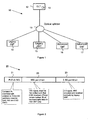
- a GPON 10 is shown schematically in Figure 1 that includes an advanced OLT 12 with a signal generator 19 capable of generating dual speed transmissions, such as a base speed of 2.5 Gb/s and a higher speed such as 10 Gb/s. Transmissions are received at an optical splitter 13 and then conveyed to individual ONTs 14, 15, 16, 17.
- ONTs 14, 15, 16, 17 may be legacy ONTs configured to receive data at the base speed or advanced ONTs configured to receive data at the higher speed.
- ONTs 14, 15 are considered to be legacy ONTs while ONTs 16, 17 are considered to be advanced ONTs.
- the base speed will be described as being at 2.5 Gb/s (2.5G) while the higher speed will be described as being at 10 Gb/s (10G), though the person skilled in the art will readily understand that other speeds may be provided for in a dual speed network.
- FIG. 2 there is shown a frame format 20 that may be transmitted by the OLT 12 on the dual speed optical network 10.
- First the OLT 12 transmits the physical layer overhead 21 at 2.5G which is read by all ONTs 14, 15, 16, 17.
- This overhead is coded using the same line code that is used by the legacy ONTs and contains the pointers to 10G and 2.5G partitions.
- a 10G partition 22 is transmitted at 10 Gb/s speed. All advanced ONTs 16, 17 receive this partition and read the data depending on the address. During this period, legacy ONTs 14, 15 are not receiving data, but must maintain their PLLs locked.
- the 10G partition is followed by a 2.5G partition 23 which is received by the legacy ONTs 14, 15 while the advanced ONTs must maintain their PLLs locked. Maintaining the lock of an advanced ONT 16, 17 during the 2.5G partition 22 is relatively simple and requires only a PLL whose run-length is 4 x N, where N is the run length of the 2.5G signal
- the line code used by the 10G partition is more complex.
- the line code used by 10G partition cannot be a traditional NRZ code, but a code that is 2.5G-friendly, while still transmitting data at 10 Gb/s.
- the line code is designed such that to the legacy ONTs 14, 15 it looks like 2.5-Gb/s data, which may be meaningless data, but still data from which the clock can be reliably recovered, and to the advanced ONTs 16, 17 it looks like meaningful 10-Gb/s data signal.
- the network 10, and more particularly the line code used by the OLT can be designed to take advantage of the known properties of the legacy ONTs.
- the legacy ONTs include a broadband optical receiver with possible wavelength block at 1550 nm (wavelength reserved for RF video overlay), a transimpedance amplifier (TIA), a limiting amplifier followed by a binary detector and a PLL designed to recover a nominal clock of 2.5 GHz.
- the bandwidth of the two amplifiers combined is slightly lower than 2.5 GHz and typically all of the components above 2.5 GHz are completely suppressed.
- Figure 3 shows the typical frequency response 30 of the legacy receiver.
- Curve 31 has been constructed by measuring the response at several points and connecting the measured data points with straight lines, while the curve 32 has been constructed by interpolating a Type-II Chebyshev filter using the measured points (i.e. mathematical model convenient for simulations).
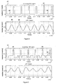
- Figure 4 shows the principles used in constructing a 2.5G-friendly signal in accordance with one embodiment of the disclosure.
- Graph 41 is a 10-Gb/s signal 42 with pilot spikes 43 repeated every 8 bits and no signal 44 in between.
- the signal 42 can be viewed as a train of 10-Gb/s pulses placed at a 1.25-GHz grid.
- the resulting signal is a 1.25-GHz sinusoid 46 shown in the graph 45.
- the signal 46 looks like a 1.25-GHz square wave having an alternating 1-0-1-0 pattern of bits transmitted at 2.5 Gb/s. This is ideal for maintaining the stable lock at the legacy receiver, but such a signal does not carry any information.
- a variant of the signal 42 is shown as signal 52 in the graph 51 of Figure 5 .
- the space 54 between pilot spikes 53 has been used to transmit 10-Gb/s data bits that are of the same duration as pilot spikes, but of much lower amplitude.
- Graph 55 of Figure 5 shows the resulting signal 56 after passing the signal 52 through the low pass filter.
- the signal 56 is distorted, but still contains a detectable 1.25GHz component necessary to maintain the 2.5-Gb/s receiver locked.
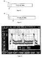
- the signal 52 contains a pilot spike followed by 7 bits of data.
- the eye pattern of such a signal is shown in Figure 6 .
- a circuit 70 that can be used in the signal generator 19 of OLT 12 to generate the signal is shown in Figure 7 and includes a 10G data signal branch 75 which is provided to combiner (summer) 77.
- an AND gate 71 has inputs from the 10G data signal branch 75 and a 2.5G clock signal branch 76, i.e. comprising the 2.5G pilot spikes, with the output of the AND gate 71 being provided to combiner 77.
- the output of AND gate 71 is forced to zero whenever the 2.5G spike is not present and to the 10G signal level whenever the spike is present.
- the upper branch 75 of the circuit is always at the 10G signal level.
- An attenuator 74 in the branch allows tuning of the ratio between the 10G eye height and the pilot spike height.
- Phase delays 72, 73 in the 2.5G and 10G branches respectively are used to tune the delays so that the pilot spike and the actual signal arrive to the combiner 77 aligned.
- the output of the combiner 77 provides the 10G signal of the first partition 22 of the frame format 20 shown in Figure 2 described above.
- the 10G signal is encoded using the 8-bit codeword 80 shown in Figure 8 , that is if the codeword whose one bit 81 is forced to 1 is the bit that coincides with the pilot spike, a signal that guarantees the spike every 8 bits is generated as shown in the eye pattern of Figure 6 .
- the AND gate 71 behaves as a pass-through element and is thus optional.
- the pilot spikes need not be present every 8 bits.
- the system may be able to afford to occasionally lose a spike.
- the location of the bit that corresponds to the pilot spike location need not be always forced to 1 and thus can be used for data. For example, if a line code 90 of Figure 9 is used in which 15 data bits 92 are allowed, a pilot spike is guaranteed every 16 bits. However, the nominal spike between two guaranteed spikes will not always exist, i.e. if the transmitted data at the nominal spike location is 0. In Figure 10 , the eye pattern using the line encoding of Figure 9 is shown.
- the signal of Figure 6 can be turned upside-down creating notches instead of spikes, which may be advantageous for some DC-coupled receivers.
- spike positions can be varied by plus/minus a few 10G bits in any way that, after low-pass filtering, allows a dominating clock component to be recovered thereby allowing the 2.5G PLL to maintain lock.
- spikes may extend for multiple bit times. For example, it is possible to have a spike at nominal position as shown in Figure 10 but with the adjacent bit also of the same height as the spike. All of these variants may be generated using the circuit of Figure 7 , as may be apparent to a person skilled in the art.
- the ratio may be different, but for each variant of modulation, a lower bound below which the receiver does not lock reliably exists.
- the amplitude of the spike is typically greater than four times the amplitude of the 10G data signal. If the spike is lower, the 10G signal dominates and the 2.5G receiver perceives it as noise to which it cannot lock. This represents a peak power penalty of 7dB and average power penalty of roughly 4dB compared to traditional 10-Gb/s NRZ signal that are not 2.5G-friendly and thus not backwards compatible with legacy receivers.
- a detection threshold must be established.
- the signal 111 shown, for example in Figure 11 appears to be a multilevel signal, the actual information is contained in two levels only.
- a possible threshold 112 is indicated with the lower signal 113 showing the detected signal. Clearly, all bits are detectable and easily recovered.
- FIG. 14 shows a circuit 140 that can be used for detection of the 10G signal.
- the lower branch 141 includes envelope detection 144 that is used to obtain a running partial average of the signal 146 and estimate the elevation of the eye.
- a phase shifter 142 and amplifier 143 in the branch 141 adjust the threshold position and level and the differential amplifier 145 is used to compare the received signal 146 against the threshold.
- the information sent between various modules can be sent between the modules via at least one of a data network, the Internet, an Internet Protocol network, a wireless source, and a wired source and via plurality of protocols.
Abstract
Description
- This invention relates to passive optical networks and in particular to 10 Gigabit-per-second passive optical networks based on the ITU-T G.984 standard which have dual speed capabilities.
- Current Gigabit/s Passive Optical Networks (GPONs) have a standard operating speed of 2.5 Gb/s. However, standards for GPONs having an operating speed of 10 Gb/s are under development which will require an upgrade of existing networks. A straightforward approach to upgrade the network is to upgrade the Optical Line Termination (OLT) from 2.5 Gb/s to 10 Gb/s and then upgrade the Optical Network Termination (ONT), sometimes referred to as an Optical Network Unit (ONU), of every subscriber. However, such an approach is likely to be prohibitively expensive. Further, the network will experience downtime until all of the subscribers are upgraded, which may be a couple of days to a couple of weeks time period.
- One alternative upgrade scenario would be to upgrade the OLT to 10 Gb/s first, but provide backwards compatibility such that legacy ONTs can interoperate with the new OLT. Thus the new OLT must also be configured to run at 2.5 Gb/s (legacy speed). Such a system is considered to be 10-Gb/s-ready, but is still not running at 10 Gb/s. The upgrades of the ONTs will occur only when the subscriber requests them, with the understanding that some subscribers may never request to upgrade and thus will remain with equipment configured for 2.5 Gb/s only.
- Thus at some stage during the upgrade, the PON system would consist of a dual-speed OLT (i.e., an OLT capable of transmitting at either 10 Gb/s or 2.5 Gb/s) and a mixture of advanced and legacy subscribers (i.e. subscribers whose ONT runs at 10 Gb/s and subscribers whose ONT runs at 2.5 Gb/s). In such a network, the dual speed OLT may be transmitting to either legacy or advanced ONT switching the speed from one to the other.
- To provide dual speed transmission, a frame format is used having consecutive 10G and 2.5G partitions. A problem with dual speed transmission is that during a 10G partition for example, legacy ONTs are not receiving data but must maintain their Phase-Locked Loops (PLL)s in a locked state, i.e. they must keep the recovered clock stable and unchanged, so that they can receive the data when the 2.5G partition starts. During the 2.5G partition, legacy ONTs are receiving data, while advanced ONTs are maintaining the recovered clock locked. If both partitions use the most commonly used non-return to Zero on-off keying (NRZ-OOK) modulation format, maintaining the clock locked by the legacy receivers during the 10G partition would not be possible due to inherent phase ambiguity that exists in every signal that is an integer times faster than the nominal signal.
- What is required is a system, method and computer readable medium capable of providing dual speed transmission in a passive optical network.
JP 2007 243796 (A
JP 2007 243796 (A - In one aspect of the disclosure, there is provided a passive optical network comprising at least one optical line termination; at least one first optical network termination operating at a first speed; at least one second optical network termination operating at a second speed slower than said first speed; wherein the at least one optical line termination transmits a data signal comprising at least one first speed partition and at least one second speed partition; wherein the at least one first speed partition comprises a signal processable by the at least one second optical network termination to extract a second speed clock signal.
- In one aspect of the disclosure, there is provided a method of communicating data on a dual speed passive optical network comprising generating a transmission signal comprising at least one first partition and at least one second partition; and transmitting said transmission signal; wherein the at least one first partition comprises a first data signal at a first speed and a clock signal at a second speed; wherein the at least one second partition comprises a second data signal at said second speed.
- In one aspect of the disclosure, there is provided an optical line termination comprising a signal generator that generates a signal comprising a first data signal at a first speed and a timing signal at a second speed.
- In one aspect of the disclosure, there is provided an optical network termination comprising a signal receiver; an extraction circuit that processes a received signal received by said signal receiver and separates a first speed data signal from a second speed timing signal.
- In one aspect of the disclosure, there is provided a method of operating an optical network termination comprising receiving a signal comprising a data signal having a first amplitude and a first signal rate and a clock signal having a second amplitude greater than said first amplitude and a second signal rate; and separating said data signal from said clock signal.
- The invention will now be described, by way of example only, with reference to specific embodiments and to the accompanying drawings in which :
-
Figure 1 schematically shows a passive optical network; -
Figure 2 schematically shows a dual speed frame format; -
Figure 3 schematically shows a frequency response of a legacy ONT; -
Figure 4 shows a 2.5G spike signal; -
Figure 5 shows a transmission signal having a 2.5G spike signal with a 10G data signal; -
Figure 6 shows a measured eye diagram corresponding to the transmission signal ofFigure 5 ; -
Figure 7 schematically shows a circuit for generating the transmission signal ofFigure 5 ; -
Figure 8 schematically shows a line encoding of one embodiment of the disclosure; -
Figure 9 schematically shows a line encoding of another embodiment of the disclosure; -
Figure 10 schematically shows a measured eye diagram corresponding to the line encoding ofFigure 9 ; -
Figure 11 schematically shows a transmission signal before and after applying threshold detection; -
Figure 12 schematically shows an eye diagram for an elevated data signal level incorporating a spike signal; -
Figure 13 shows an expanded view of the eye diagram ofFigure 12 ; and -
Figure 14 schematically shows a circuit for detecting a data signal using a modulating threshold. - A
GPON 10 is shown schematically inFigure 1 that includes anadvanced OLT 12 with asignal generator 19 capable of generating dual speed transmissions, such as a base speed of 2.5 Gb/s and a higher speed such as 10 Gb/s. Transmissions are received at anoptical splitter 13 and then conveyed toindividual ONTs - In
Figure 2 , there is shown aframe format 20 that may be transmitted by theOLT 12 on the dual speedoptical network 10. First theOLT 12 transmits thephysical layer overhead 21 at 2.5G which is read by allONTs - After the
overhead 21, a10G partition 22 is transmitted at 10 Gb/s speed. Alladvanced ONTs - The 10G partition is followed by a 2.5
G partition 23 which is received by the legacy ONTs 14, 15 while the advanced ONTs must maintain their PLLs locked. Maintaining the lock of anadvanced ONT G partition 22 is relatively simple and requires only a PLL whose run-length is 4 x N, where N is the run length of the 2.5G signal - However, the line code used by the 10G partition is more complex. The line code used by 10G partition cannot be a traditional NRZ code, but a code that is 2.5G-friendly, while still transmitting data at 10 Gb/s. In an embodiment of the disclosure, the line code is designed such that to the legacy ONTs 14, 15 it looks like 2.5-Gb/s data, which may be meaningless data, but still data from which the clock can be reliably recovered, and to the
advanced ONTs - The
network 10, and more particularly the line code used by the OLT, can be designed to take advantage of the known properties of the legacy ONTs. In particular, the legacy ONTs include a broadband optical receiver with possible wavelength block at 1550 nm (wavelength reserved for RF video overlay), a transimpedance amplifier (TIA), a limiting amplifier followed by a binary detector and a PLL designed to recover a nominal clock of 2.5 GHz. The bandwidth of the two amplifiers combined is slightly lower than 2.5 GHz and typically all of the components above 2.5 GHz are completely suppressed. -
Figure 3 shows thetypical frequency response 30 of the legacy receiver.Curve 31 has been constructed by measuring the response at several points and connecting the measured data points with straight lines, while thecurve 32 has been constructed by interpolating a Type-II Chebyshev filter using the measured points (i.e. mathematical model convenient for simulations). -
Figure 4 shows the principles used in constructing a 2.5G-friendly signal in accordance with one embodiment of the disclosure.Graph 41 is a 10-Gb/ssignal 42 withpilot spikes 43 repeated every 8 bits and nosignal 44 in between. Thus, thesignal 42 can be viewed as a train of 10-Gb/s pulses placed at a 1.25-GHz grid. When such a signal is passed through the simulating filter described with reference toFigure 3 , the resulting signal is a 1.25-GHz sinusoid 46 shown in thegraph 45. When detected by a binary detector, thesignal 46 looks like a 1.25-GHz square wave having an alternating 1-0-1-0 pattern of bits transmitted at 2.5 Gb/s. This is ideal for maintaining the stable lock at the legacy receiver, but such a signal does not carry any information. - A variant of the
signal 42 is shown assignal 52 in thegraph 51 ofFigure 5 . In thesignal 52, thespace 54 between pilot spikes 53 has been used to transmit 10-Gb/s data bits that are of the same duration as pilot spikes, but of much lower amplitude. Graph 55 ofFigure 5 shows the resulting signal 56 after passing thesignal 52 through the low pass filter. The signal 56 is distorted, but still contains a detectable 1.25GHz component necessary to maintain the 2.5-Gb/s receiver locked. - The
signal 52 contains a pilot spike followed by 7 bits of data. The eye pattern of such a signal is shown inFigure 6 . Acircuit 70 that can be used in thesignal generator 19 ofOLT 12 to generate the signal is shown inFigure 7 and includes a 10G data signalbranch 75 which is provided to combiner (summer) 77. In the lower branch, an ANDgate 71 has inputs from the 10G data signalbranch 75 and a 2.5Gclock signal branch 76, i.e. comprising the 2.5G pilot spikes, with the output of the ANDgate 71 being provided tocombiner 77. - The output of AND
gate 71 is forced to zero whenever the 2.5G spike is not present and to the 10G signal level whenever the spike is present. Theupper branch 75 of the circuit is always at the 10G signal level. Anattenuator 74 in the branch allows tuning of the ratio between the 10G eye height and the pilot spike height. Phase delays 72, 73 in the 2.5G and 10G branches respectively are used to tune the delays so that the pilot spike and the actual signal arrive to thecombiner 77 aligned. The output of thecombiner 77 provides the 10G signal of thefirst partition 22 of theframe format 20 shown inFigure 2 described above. - If the 10G signal is encoded using the 8-
bit codeword 80 shown inFigure 8 , that is if the codeword whose onebit 81 is forced to 1 is the bit that coincides with the pilot spike, a signal that guarantees the spike every 8 bits is generated as shown in the eye pattern ofFigure 6 . In this case, the ANDgate 71 behaves as a pass-through element and is thus optional. - However, the pilot spikes need not be present every 8 bits. Depending on the PLL type used at the legacy receiver, the system may be able to afford to occasionally lose a spike. In one embodiment, the location of the bit that corresponds to the pilot spike location need not be always forced to 1 and thus can be used for data. For example, if a
line code 90 ofFigure 9 is used in which 15data bits 92 are allowed, a pilot spike is guaranteed every 16 bits. However, the nominal spike between two guaranteed spikes will not always exist, i.e. if the transmitted data at the nominal spike location is 0. InFigure 10 , the eye pattern using the line encoding ofFigure 9 is shown. Comparing the eye pattern ofFigure 10 with the eye pattern ofFigure 6 , it is observed that thespike 61 inFigure 6 is always 1, while the spike in the middle ofFigure 10 is sometimes ofnominal spike height 101 and sometimes 0 (102). If the 10G data is scrambled (resulting in almost equal probability of having 1 or 0), approximately 50% of the 16-bit periods contain the spike at 8-bit grid, while the other 50% do not contain the middle spike. In this way the coding overhead can be reduced. - Other variations of the principles disclosed above are also possible. For example, the signal of
Figure 6 can be turned upside-down creating notches instead of spikes, which may be advantageous for some DC-coupled receivers. Further, spike positions can be varied by plus/minus a few 10G bits in any way that, after low-pass filtering, allows a dominating clock component to be recovered thereby allowing the 2.5G PLL to maintain lock. Also, spikes may extend for multiple bit times. For example, it is possible to have a spike at nominal position as shown inFigure 10 but with the adjacent bit also of the same height as the spike. All of these variants may be generated using the circuit ofFigure 7 , as may be apparent to a person skilled in the art. - Experiments with a standard (2.5-Gb/s) GPON receiver have shown that a variety of power/bit-rate/error-rate/reliability trade-offs are possible. One specific class of experiments has shown that it is possible to lose every other spike with relatively small power penalty, which is the rationale for the line code of
Figure 9 . In general the effect on the legacy GPON ONT is that the spike has to be stronger by a certain ratio for the legacy receiver to remain locked. The experiments for a spike width of 1 bit time, square shape and a guaranteed spike every 8 bits have shown that this ratio needs to be about 5x or 7dB; that is, the ratio between the spike height and the 10G eye height needs to be greater than 7dB. For different spike widths, shapes and frequencies, the ratio may be different, but for each variant of modulation, a lower bound below which the receiver does not lock reliably exists. In one embodiment, the amplitude of the spike is typically greater than four times the amplitude of the 10G data signal. If the spike is lower, the 10G signal dominates and the 2.5G receiver perceives it as noise to which it cannot lock. This represents a peak power penalty of 7dB and average power penalty of roughly 4dB compared to traditional 10-Gb/s NRZ signal that are not 2.5G-friendly and thus not backwards compatible with legacy receivers. - To detect the 10-Gb/s signal in the
advanced ONTs network 10, a detection threshold must be established. Although thesignal 111 shown, for example inFigure 11 , appears to be a multilevel signal, the actual information is contained in two levels only. Apossible threshold 112 is indicated with thelower signal 113 showing the detected signal. Clearly, all bits are detectable and easily recovered. - Accurate signal detection using a flat threshold typically requires expensive and high-quality components that create a clean signal, which is not necessarily practical as such components require wide bandwidth, wide dynamic range (i.e. linearity) and low noise. One of the effects seen when lower-quality components are used, shown in
Figure 12 , is the elevation of the10G bit 122 that is adjacent to thepilot spike 121. The effect comes from the finite bandwidth of the components used. That is, in the vicinity of the pilot-spike, components are responding similarly as they would respond to the delta-pulse, and thus it takes a finite time to settle. The area of interest is shown in expanded view inFigure 13 . Importantly, a zerolevel bit 124 is observed to cross theflat threshold 123 and would therefore be erroneously detected as a 1 level bit. In one embodiment, athreshold 125 that tracks the elevations of the eye is used so that the problematic bits can be decoded more reliably.Figure 14 shows acircuit 140 that can be used for detection of the 10G signal. Thelower branch 141 includesenvelope detection 144 that is used to obtain a running partial average of thesignal 146 and estimate the elevation of the eye. Aphase shifter 142 andamplifier 143 in thebranch 141 adjust the threshold position and level and thedifferential amplifier 145 is used to compare the receivedsignal 146 against the threshold. - Although embodiments of the present invention have been illustrated in the accompanied drawings and described in the foregoing description, it will be understood that the invention is not limited to the embodiments disclosed, but is capable of numerous rearrangements, modifications, and substitutions without departing from the spirit of the invention as set forth and defined by the following claims. For example, the capabilities of the invention can be performed fully and/or partially by one or more of the blocks, modules, processors or memories. Also, these capabilities may be performed in the current manner or in a distributed manner and on, or via, any device able to provide and/or receive information. Further, although depicted in a particular manner, various modules or blocks may be repositioned without departing from the scope of the current invention. Still further, although depicted in a particular manner, a greater or lesser number of modules and connections can be utilized with the present invention in order to accomplish the present invention, to provide additional known features to the present invention, and/or to make the present invention more efficient. Also, the information sent between various modules can be sent between the modules via at least one of a data network, the Internet, an Internet Protocol network, a wireless source, and a wired source and via plurality of protocols.
Claims (10)
- A passive optical network (10) comprising:at least one optical line termination (12);at least one first optical network termination adapted to operate at a first speed (16, 17);at least one second optical network termination (14, 15) adapted to operate at a second speed slower than said first speed;wherein the at least one optical line termination (12) is adapted to transmit a data signal (20) comprising at least one first speed partition (22) and at least one second speed partition (23),wherein the at least one second optical network termination (14,15) is adapted to extract a second speed clock signal (53) from the at least one first speed partition of the signal transmitted by the optical line termination.
- The passive optical network (10) according to claim 1 wherein the at least one first partition (22) comprises a first speed data signal (54) and a second speed clock signal (53).
- The passive optical network (10) according to claim 2 wherein an amplitude of said second speed clock signal (53) is greater than an amplitude of said first speed data signal (54).
- The passive optical network (10) according to claim 3 wherein the amplitude of said second speed clock signal (53) is greater than four times the amplitude of said first speed data signal (54).
- The passive optical network (10) according to claim 2 wherein the at least one first optical network termination (16, 17) comprises a detection circuit (140) that determines a threshold (125) and compares the first speed partition (22) to said threshold (125) to extract said first speed data signal (54).
- The passive optical network (10) of claim 5 wherein the detection circuit (140) comprises an averaging circuit (144) that determines said threshold (125) using an at least partial average of said first speed partition (22).
- The passive optical network (10) of claim 1 wherein the at least one optical line termination (12) comprises a signal generator (70) comprising a combiner (77), a first input of said combiner (77) comprising a first speed data signal (75) and a second input of said combiner (77) comprising said second speed clock signal (76).
- The passive optical network (10) of claim 7 wherein said signal generator (70) further comprises an attenuator (74) that controls the ratio of the first speed data signal (75) and the second speed clock signal (76).
- The passive optical network (10) of claim 7 wherein said signal generator (70) further comprises an AND gate (71), a first input of said AND gate (71) comprising said first speed data signal (75) and a second input of said AND gate (71) comprising said second speed clock signal (76).
- The passive optical network (10) of claim 9 wherein said second input of said combiner (77) comprises an output of said AND gate (71).
Applications Claiming Priority (2)
| Application Number | Priority Date | Filing Date | Title |
|---|---|---|---|
| US12/074,692 US9225425B2 (en) | 2008-03-05 | 2008-03-05 | System and method for dual speed passive optical networks |
| PCT/US2009/001141 WO2009110967A1 (en) | 2008-03-05 | 2009-02-24 | System and method for dual speed passive optical networks |
Publications (2)
| Publication Number | Publication Date |
|---|---|
| EP2260595A1 EP2260595A1 (en) | 2010-12-15 |
| EP2260595B1 true EP2260595B1 (en) | 2012-06-06 |
Family
ID=40589825
Family Applications (1)
| Application Number | Title | Priority Date | Filing Date |
|---|---|---|---|
| EP09716994A Not-in-force EP2260595B1 (en) | 2008-03-05 | 2009-02-24 | System and method for dual speed passive optical networks |
Country Status (5)
| Country | Link |
|---|---|
| US (1) | US9225425B2 (en) |
| EP (1) | EP2260595B1 (en) |
| KR (1) | KR101159521B1 (en) |
| CN (1) | CN101960744A (en) |
| WO (1) | WO2009110967A1 (en) |
Families Citing this family (5)
| Publication number | Priority date | Publication date | Assignee | Title |
|---|---|---|---|---|
| US9031408B2 (en) | 2011-06-09 | 2015-05-12 | Telefonaktiebolaget L M Ericsson (Publ) | Method for fast wavelength division multiplexing (WDM) passive optical network (PON) initialization in heterogeneous networks |
| US8548328B2 (en) * | 2011-09-08 | 2013-10-01 | Telefonaktiebolaget L M Ericsson (Publ) | Transparent overhead in a passive optical network that supports enhanced features |
| CN104937863A (en) * | 2013-12-23 | 2015-09-23 | 华为技术有限公司 | Method and device for upgrading system |
| CN112583507B (en) | 2019-09-29 | 2022-05-10 | 华为技术有限公司 | State control method, data sending method and terminal |
| US11902720B2 (en) * | 2022-03-01 | 2024-02-13 | Nokia Solutions And Networks Oy | Method and apparatus for downstream timeslot scheduling in multi-rate passive optical networks |
Family Cites Families (10)
| Publication number | Priority date | Publication date | Assignee | Title |
|---|---|---|---|---|
| US5917979A (en) * | 1996-12-26 | 1999-06-29 | The Trustees Of Princeton University | Asymmetric optical loop mirror exhibiting threshold discrimination for separation of input pulses of differing magnitudes |
| US7058315B2 (en) * | 2001-10-09 | 2006-06-06 | Chiaro Networks Ltd. | Fast decision threshold controller for burst-mode receiver |
| KR100575981B1 (en) * | 2003-06-11 | 2006-05-02 | 삼성전자주식회사 | Peak detector and bottom detector of burst-mode optical receiver |
| CN100414904C (en) * | 2004-12-17 | 2008-08-27 | 电子科技大学 | Ether passive optical network uplink access method |
| CA2866063C (en) | 2005-03-02 | 2016-05-17 | 3 Phoenix, Inc. | An inverted passive optical network/inverted passive electrical network (ipon/ipen) based data fusion and synchronization system |
| JP2007243796A (en) | 2006-03-10 | 2007-09-20 | Sumitomo Electric Ind Ltd | Multi-rate pon system and terminal device used therefor |
| JP5017942B2 (en) * | 2006-06-30 | 2012-09-05 | 富士通株式会社 | Bit rate mixed optical communication method, optical subscriber unit and optical station side unit |
| JP4882614B2 (en) * | 2006-09-01 | 2012-02-22 | 富士通株式会社 | Bit rate mixed optical communication method, optical subscriber unit and optical station side unit |
| IL178744A0 (en) * | 2006-10-19 | 2007-09-20 | Eci Telecom Ltd | Method for estimating bandwidth limiting effects in transmission communication systems |
| JP4823110B2 (en) * | 2007-03-15 | 2011-11-24 | 富士通株式会社 | Passive optical network system and data transmission method in passive optical network |
-
2008
- 2008-03-05 US US12/074,692 patent/US9225425B2/en not_active Expired - Fee Related
-
2009
- 2009-02-24 WO PCT/US2009/001141 patent/WO2009110967A1/en active Application Filing
- 2009-02-24 KR KR1020107021975A patent/KR101159521B1/en active IP Right Grant
- 2009-02-24 CN CN2009801075163A patent/CN101960744A/en active Pending
- 2009-02-24 EP EP09716994A patent/EP2260595B1/en not_active Not-in-force
Also Published As
| Publication number | Publication date |
|---|---|
| KR20100134634A (en) | 2010-12-23 |
| WO2009110967A1 (en) | 2009-09-11 |
| US9225425B2 (en) | 2015-12-29 |
| US20090226182A1 (en) | 2009-09-10 |
| WO2009110967A8 (en) | 2010-10-07 |
| EP2260595A1 (en) | 2010-12-15 |
| KR101159521B1 (en) | 2012-06-25 |
| CN101960744A (en) | 2011-01-26 |
Similar Documents
| Publication | Publication Date | Title |
|---|---|---|
| CN110771067B (en) | Optical receiver, optical transmitter, data identification method, and multilevel communication system | |
| EP2260595B1 (en) | System and method for dual speed passive optical networks | |
| EP2830239B1 (en) | Method, system and transceiver device for bi-directionally transmitting digital optical signals over an optical transmission link | |
| CN110870246B (en) | Frequency/phase shift keying for backchannel SERDES communications | |
| US20040170439A1 (en) | Method and apparatus for an optical cdma system | |
| JP2007243796A (en) | Multi-rate pon system and terminal device used therefor | |
| RU2676406C1 (en) | Method and device for fixing errors and passive optical network | |
| CN105991196B (en) | A kind of data precoding device, system and coding method | |
| CN101521555B (en) | Code division multiplex communication system | |
| US8009993B2 (en) | Hybrid balanced coding scheme | |
| US8538271B2 (en) | Combined burst mode level and clock recovery | |
| KR102009985B1 (en) | Communication system based on ethernet | |
| WO2019160838A1 (en) | Multi-rate optical network | |
| CN101013930A (en) | Optical access network system | |
| US9467316B2 (en) | Method and device for transmitting a low-frequency signal over a data transmission link using a digital high bit-rate signal | |
| US7369600B2 (en) | Burst communications apparatus and method using tapped delay lines | |
| EP3641169A1 (en) | Data processing method, optical line terminal, optical network unit and system | |
| EP0924907A2 (en) | Multiplexed transmission using PAM | |
| KR101023813B1 (en) | Registration method for ONU or ONT | |
| KR20120018086A (en) | Method and apparatus for burst mode clock and data recovery | |
| CN107534628A (en) | A kind of circuit, method and the optical network unit of acquisition PAM4 decoding threshold value | |
| Kourtessis et al. | A complete 8-GHz QPSK-MODEM featuring novel subcarrier and data synchronization for optical communications | |
| US8014405B2 (en) | Upgrading ATM embedded networks to carry IP signals | |
| Lawin et al. | Direct Digital Modulated Message Channel for Passive Metro WDM Systems | |
| WO2020210423A2 (en) | Electrical duobinary soft information receiver for nrz modulation fiber transmission |
Legal Events
| Date | Code | Title | Description |
|---|---|---|---|
| PUAI | Public reference made under article 153(3) epc to a published international application that has entered the european phase |
Free format text: ORIGINAL CODE: 0009012 |
|
| 17P | Request for examination filed |
Effective date: 20101005 |
|
| AK | Designated contracting states |
Kind code of ref document: A1 Designated state(s): AT BE BG CH CY CZ DE DK EE ES FI FR GB GR HR HU IE IS IT LI LT LU LV MC MK MT NL NO PL PT RO SE SI SK TR |
|
| AX | Request for extension of the european patent |
Extension state: AL BA RS |
|
| DAX | Request for extension of the european patent (deleted) | ||
| REG | Reference to a national code |
Ref country code: DE Ref legal event code: R079 Ref document number: 602009007485 Country of ref document: DE Free format text: PREVIOUS MAIN CLASS: H04B0010200000 Ipc: H04L0025060000 |
|
| GRAP | Despatch of communication of intention to grant a patent |
Free format text: ORIGINAL CODE: EPIDOSNIGR1 |
|
| RIC1 | Information provided on ipc code assigned before grant |
Ipc: H04B 10/20 20060101ALI20111108BHEP Ipc: H04J 3/00 20060101ALI20111108BHEP Ipc: H04Q 11/00 20060101ALI20111108BHEP Ipc: H04L 25/06 20060101AFI20111108BHEP |
|
| RAP1 | Party data changed (applicant data changed or rights of an application transferred) |
Owner name: ALCATEL LUCENT |
|
| GRAS | Grant fee paid |
Free format text: ORIGINAL CODE: EPIDOSNIGR3 |
|
| GRAA | (expected) grant |
Free format text: ORIGINAL CODE: 0009210 |
|
| AK | Designated contracting states |
Kind code of ref document: B1 Designated state(s): AT BE BG CH CY CZ DE DK EE ES FI FR GB GR HR HU IE IS IT LI LT LU LV MC MK MT NL NO PL PT RO SE SI SK TR |
|
| REG | Reference to a national code |
Ref country code: GB Ref legal event code: FG4D |
|
| REG | Reference to a national code |
Ref country code: AT Ref legal event code: REF Ref document number: 561477 Country of ref document: AT Kind code of ref document: T Effective date: 20120615 Ref country code: CH Ref legal event code: EP |
|
| REG | Reference to a national code |
Ref country code: IE Ref legal event code: FG4D |
|
| REG | Reference to a national code |
Ref country code: DE Ref legal event code: R096 Ref document number: 602009007485 Country of ref document: DE Effective date: 20120802 |
|
| REG | Reference to a national code |
Ref country code: NL Ref legal event code: VDEP Effective date: 20120606 |
|
| PG25 | Lapsed in a contracting state [announced via postgrant information from national office to epo] |
Ref country code: NO Free format text: LAPSE BECAUSE OF FAILURE TO SUBMIT A TRANSLATION OF THE DESCRIPTION OR TO PAY THE FEE WITHIN THE PRESCRIBED TIME-LIMIT Effective date: 20120906 Ref country code: FI Free format text: LAPSE BECAUSE OF FAILURE TO SUBMIT A TRANSLATION OF THE DESCRIPTION OR TO PAY THE FEE WITHIN THE PRESCRIBED TIME-LIMIT Effective date: 20120606 Ref country code: CY Free format text: LAPSE BECAUSE OF FAILURE TO SUBMIT A TRANSLATION OF THE DESCRIPTION OR TO PAY THE FEE WITHIN THE PRESCRIBED TIME-LIMIT Effective date: 20120606 Ref country code: LT Free format text: LAPSE BECAUSE OF FAILURE TO SUBMIT A TRANSLATION OF THE DESCRIPTION OR TO PAY THE FEE WITHIN THE PRESCRIBED TIME-LIMIT Effective date: 20120606 Ref country code: SE Free format text: LAPSE BECAUSE OF FAILURE TO SUBMIT A TRANSLATION OF THE DESCRIPTION OR TO PAY THE FEE WITHIN THE PRESCRIBED TIME-LIMIT Effective date: 20120606 |
|
| REG | Reference to a national code |
Ref country code: AT Ref legal event code: MK05 Ref document number: 561477 Country of ref document: AT Kind code of ref document: T Effective date: 20120606 |
|
| REG | Reference to a national code |
Ref country code: LT Ref legal event code: MG4D Effective date: 20120606 |
|
| PG25 | Lapsed in a contracting state [announced via postgrant information from national office to epo] |
Ref country code: LV Free format text: LAPSE BECAUSE OF FAILURE TO SUBMIT A TRANSLATION OF THE DESCRIPTION OR TO PAY THE FEE WITHIN THE PRESCRIBED TIME-LIMIT Effective date: 20120606 Ref country code: SI Free format text: LAPSE BECAUSE OF FAILURE TO SUBMIT A TRANSLATION OF THE DESCRIPTION OR TO PAY THE FEE WITHIN THE PRESCRIBED TIME-LIMIT Effective date: 20120606 Ref country code: GR Free format text: LAPSE BECAUSE OF FAILURE TO SUBMIT A TRANSLATION OF THE DESCRIPTION OR TO PAY THE FEE WITHIN THE PRESCRIBED TIME-LIMIT Effective date: 20120907 Ref country code: HR Free format text: LAPSE BECAUSE OF FAILURE TO SUBMIT A TRANSLATION OF THE DESCRIPTION OR TO PAY THE FEE WITHIN THE PRESCRIBED TIME-LIMIT Effective date: 20120606 |
|
| PG25 | Lapsed in a contracting state [announced via postgrant information from national office to epo] |
Ref country code: IS Free format text: LAPSE BECAUSE OF FAILURE TO SUBMIT A TRANSLATION OF THE DESCRIPTION OR TO PAY THE FEE WITHIN THE PRESCRIBED TIME-LIMIT Effective date: 20121006 Ref country code: SK Free format text: LAPSE BECAUSE OF FAILURE TO SUBMIT A TRANSLATION OF THE DESCRIPTION OR TO PAY THE FEE WITHIN THE PRESCRIBED TIME-LIMIT Effective date: 20120606 Ref country code: BE Free format text: LAPSE BECAUSE OF FAILURE TO SUBMIT A TRANSLATION OF THE DESCRIPTION OR TO PAY THE FEE WITHIN THE PRESCRIBED TIME-LIMIT Effective date: 20120606 Ref country code: CZ Free format text: LAPSE BECAUSE OF FAILURE TO SUBMIT A TRANSLATION OF THE DESCRIPTION OR TO PAY THE FEE WITHIN THE PRESCRIBED TIME-LIMIT Effective date: 20120606 Ref country code: EE Free format text: LAPSE BECAUSE OF FAILURE TO SUBMIT A TRANSLATION OF THE DESCRIPTION OR TO PAY THE FEE WITHIN THE PRESCRIBED TIME-LIMIT Effective date: 20120606 Ref country code: AT Free format text: LAPSE BECAUSE OF FAILURE TO SUBMIT A TRANSLATION OF THE DESCRIPTION OR TO PAY THE FEE WITHIN THE PRESCRIBED TIME-LIMIT Effective date: 20120606 Ref country code: RO Free format text: LAPSE BECAUSE OF FAILURE TO SUBMIT A TRANSLATION OF THE DESCRIPTION OR TO PAY THE FEE WITHIN THE PRESCRIBED TIME-LIMIT Effective date: 20120606 Ref country code: NL Free format text: LAPSE BECAUSE OF FAILURE TO SUBMIT A TRANSLATION OF THE DESCRIPTION OR TO PAY THE FEE WITHIN THE PRESCRIBED TIME-LIMIT Effective date: 20120606 |
|
| PG25 | Lapsed in a contracting state [announced via postgrant information from national office to epo] |
Ref country code: IT Free format text: LAPSE BECAUSE OF FAILURE TO SUBMIT A TRANSLATION OF THE DESCRIPTION OR TO PAY THE FEE WITHIN THE PRESCRIBED TIME-LIMIT Effective date: 20120606 Ref country code: PT Free format text: LAPSE BECAUSE OF FAILURE TO SUBMIT A TRANSLATION OF THE DESCRIPTION OR TO PAY THE FEE WITHIN THE PRESCRIBED TIME-LIMIT Effective date: 20121008 Ref country code: PL Free format text: LAPSE BECAUSE OF FAILURE TO SUBMIT A TRANSLATION OF THE DESCRIPTION OR TO PAY THE FEE WITHIN THE PRESCRIBED TIME-LIMIT Effective date: 20120606 |
|
| PLBE | No opposition filed within time limit |
Free format text: ORIGINAL CODE: 0009261 |
|
| STAA | Information on the status of an ep patent application or granted ep patent |
Free format text: STATUS: NO OPPOSITION FILED WITHIN TIME LIMIT |
|
| PG25 | Lapsed in a contracting state [announced via postgrant information from national office to epo] |
Ref country code: DK Free format text: LAPSE BECAUSE OF FAILURE TO SUBMIT A TRANSLATION OF THE DESCRIPTION OR TO PAY THE FEE WITHIN THE PRESCRIBED TIME-LIMIT Effective date: 20120606 Ref country code: ES Free format text: LAPSE BECAUSE OF FAILURE TO SUBMIT A TRANSLATION OF THE DESCRIPTION OR TO PAY THE FEE WITHIN THE PRESCRIBED TIME-LIMIT Effective date: 20120917 |
|
| 26N | No opposition filed |
Effective date: 20130307 |
|
| REG | Reference to a national code |
Ref country code: DE Ref legal event code: R097 Ref document number: 602009007485 Country of ref document: DE Effective date: 20130307 |
|
| PG25 | Lapsed in a contracting state [announced via postgrant information from national office to epo] |
Ref country code: BG Free format text: LAPSE BECAUSE OF FAILURE TO SUBMIT A TRANSLATION OF THE DESCRIPTION OR TO PAY THE FEE WITHIN THE PRESCRIBED TIME-LIMIT Effective date: 20120906 |
|
| PG25 | Lapsed in a contracting state [announced via postgrant information from national office to epo] |
Ref country code: MC Free format text: LAPSE BECAUSE OF NON-PAYMENT OF DUE FEES Effective date: 20130228 |
|
| REG | Reference to a national code |
Ref country code: CH Ref legal event code: PL |
|
| REG | Reference to a national code |
Ref country code: GB Ref legal event code: 732E Free format text: REGISTERED BETWEEN 20130926 AND 20131002 |
|
| PG25 | Lapsed in a contracting state [announced via postgrant information from national office to epo] |
Ref country code: CH Free format text: LAPSE BECAUSE OF NON-PAYMENT OF DUE FEES Effective date: 20130228 Ref country code: LI Free format text: LAPSE BECAUSE OF NON-PAYMENT OF DUE FEES Effective date: 20130228 |
|
| REG | Reference to a national code |
Ref country code: FR Ref legal event code: GC Effective date: 20131018 |
|
| REG | Reference to a national code |
Ref country code: IE Ref legal event code: MM4A |
|
| PG25 | Lapsed in a contracting state [announced via postgrant information from national office to epo] |
Ref country code: IE Free format text: LAPSE BECAUSE OF NON-PAYMENT OF DUE FEES Effective date: 20130224 |
|
| PG25 | Lapsed in a contracting state [announced via postgrant information from national office to epo] |
Ref country code: MT Free format text: LAPSE BECAUSE OF FAILURE TO SUBMIT A TRANSLATION OF THE DESCRIPTION OR TO PAY THE FEE WITHIN THE PRESCRIBED TIME-LIMIT Effective date: 20120606 |
|
| REG | Reference to a national code |
Ref country code: FR Ref legal event code: RG Effective date: 20141016 |
|
| REG | Reference to a national code |
Ref country code: FR Ref legal event code: PLFP Year of fee payment: 7 |
|
| PG25 | Lapsed in a contracting state [announced via postgrant information from national office to epo] |
Ref country code: TR Free format text: LAPSE BECAUSE OF FAILURE TO SUBMIT A TRANSLATION OF THE DESCRIPTION OR TO PAY THE FEE WITHIN THE PRESCRIBED TIME-LIMIT Effective date: 20120606 |
|
| PG25 | Lapsed in a contracting state [announced via postgrant information from national office to epo] |
Ref country code: LU Free format text: LAPSE BECAUSE OF NON-PAYMENT OF DUE FEES Effective date: 20130224 Ref country code: MK Free format text: LAPSE BECAUSE OF FAILURE TO SUBMIT A TRANSLATION OF THE DESCRIPTION OR TO PAY THE FEE WITHIN THE PRESCRIBED TIME-LIMIT Effective date: 20120606 Ref country code: HU Free format text: LAPSE BECAUSE OF FAILURE TO SUBMIT A TRANSLATION OF THE DESCRIPTION OR TO PAY THE FEE WITHIN THE PRESCRIBED TIME-LIMIT; INVALID AB INITIO Effective date: 20090224 |
|
| REG | Reference to a national code |
Ref country code: FR Ref legal event code: PLFP Year of fee payment: 8 |
|
| REG | Reference to a national code |
Ref country code: FR Ref legal event code: PLFP Year of fee payment: 9 |
|
| REG | Reference to a national code |
Ref country code: FR Ref legal event code: PLFP Year of fee payment: 10 |
|
| PGFP | Annual fee paid to national office [announced via postgrant information from national office to epo] |
Ref country code: DE Payment date: 20190212 Year of fee payment: 11 Ref country code: FR Payment date: 20190111 Year of fee payment: 11 Ref country code: GB Payment date: 20190220 Year of fee payment: 11 |
|
| REG | Reference to a national code |
Ref country code: DE Ref legal event code: R119 Ref document number: 602009007485 Country of ref document: DE |
|
| GBPC | Gb: european patent ceased through non-payment of renewal fee |
Effective date: 20200224 |
|
| PG25 | Lapsed in a contracting state [announced via postgrant information from national office to epo] |
Ref country code: FR Free format text: LAPSE BECAUSE OF NON-PAYMENT OF DUE FEES Effective date: 20200229 Ref country code: GB Free format text: LAPSE BECAUSE OF NON-PAYMENT OF DUE FEES Effective date: 20200224 Ref country code: DE Free format text: LAPSE BECAUSE OF NON-PAYMENT OF DUE FEES Effective date: 20200901 |