EP2256815A2 - Semiconductor device with surrounding gate - Google Patents
Semiconductor device with surrounding gate Download PDFInfo
- Publication number
- EP2256815A2 EP2256815A2 EP10005650A EP10005650A EP2256815A2 EP 2256815 A2 EP2256815 A2 EP 2256815A2 EP 10005650 A EP10005650 A EP 10005650A EP 10005650 A EP10005650 A EP 10005650A EP 2256815 A2 EP2256815 A2 EP 2256815A2
- Authority
- EP
- European Patent Office
- Prior art keywords
- silicon pillar
- conductive type
- impurity region
- semiconductor device
- cutting
- Prior art date
- Legal status (The legal status is an assumption and is not a legal conclusion. Google has not performed a legal analysis and makes no representation as to the accuracy of the status listed.)
- Withdrawn
Links
Images























Classifications
-
- H—ELECTRICITY
- H10—SEMICONDUCTOR DEVICES; ELECTRIC SOLID-STATE DEVICES NOT OTHERWISE PROVIDED FOR
- H10D—INORGANIC ELECTRIC SEMICONDUCTOR DEVICES
- H10D64/00—Electrodes of devices having potential barriers
- H10D64/20—Electrodes characterised by their shapes, relative sizes or dispositions
- H10D64/27—Electrodes not carrying the current to be rectified, amplified, oscillated or switched, e.g. gates
- H10D64/311—Gate electrodes for field-effect devices
- H10D64/411—Gate electrodes for field-effect devices for FETs
- H10D64/511—Gate electrodes for field-effect devices for FETs for IGFETs
- H10D64/517—Gate electrodes for field-effect devices for FETs for IGFETs characterised by the conducting layers
- H10D64/519—Gate electrodes for field-effect devices for FETs for IGFETs characterised by the conducting layers characterised by their top-view geometrical layouts
-
- H—ELECTRICITY
- H10—SEMICONDUCTOR DEVICES; ELECTRIC SOLID-STATE DEVICES NOT OTHERWISE PROVIDED FOR
- H10D—INORGANIC ELECTRIC SEMICONDUCTOR DEVICES
- H10D62/00—Semiconductor bodies, or regions thereof, of devices having potential barriers
- H10D62/10—Shapes, relative sizes or dispositions of the regions of the semiconductor bodies; Shapes of the semiconductor bodies
- H10D62/13—Semiconductor regions connected to electrodes carrying current to be rectified, amplified or switched, e.g. source or drain regions
- H10D62/149—Source or drain regions of field-effect devices
- H10D62/151—Source or drain regions of field-effect devices of IGFETs
- H10D62/152—Source regions of DMOS transistors
- H10D62/153—Impurity concentrations or distributions
-
- H—ELECTRICITY
- H10—SEMICONDUCTOR DEVICES; ELECTRIC SOLID-STATE DEVICES NOT OTHERWISE PROVIDED FOR
- H10D—INORGANIC ELECTRIC SEMICONDUCTOR DEVICES
- H10D30/00—Field-effect transistors [FET]
- H10D30/01—Manufacture or treatment
- H10D30/021—Manufacture or treatment of FETs having insulated gates [IGFET]
- H10D30/025—Manufacture or treatment of FETs having insulated gates [IGFET] of vertical IGFETs
-
- H—ELECTRICITY
- H10—SEMICONDUCTOR DEVICES; ELECTRIC SOLID-STATE DEVICES NOT OTHERWISE PROVIDED FOR
- H10D—INORGANIC ELECTRIC SEMICONDUCTOR DEVICES
- H10D30/00—Field-effect transistors [FET]
- H10D30/01—Manufacture or treatment
- H10D30/021—Manufacture or treatment of FETs having insulated gates [IGFET]
- H10D30/031—Manufacture or treatment of FETs having insulated gates [IGFET] of thin-film transistors [TFT]
-
- H—ELECTRICITY
- H10—SEMICONDUCTOR DEVICES; ELECTRIC SOLID-STATE DEVICES NOT OTHERWISE PROVIDED FOR
- H10D—INORGANIC ELECTRIC SEMICONDUCTOR DEVICES
- H10D30/00—Field-effect transistors [FET]
- H10D30/60—Insulated-gate field-effect transistors [IGFET]
- H10D30/63—Vertical IGFETs
-
- H—ELECTRICITY
- H10—SEMICONDUCTOR DEVICES; ELECTRIC SOLID-STATE DEVICES NOT OTHERWISE PROVIDED FOR
- H10D—INORGANIC ELECTRIC SEMICONDUCTOR DEVICES
- H10D30/00—Field-effect transistors [FET]
- H10D30/60—Insulated-gate field-effect transistors [IGFET]
- H10D30/67—Thin-film transistors [TFT]
- H10D30/6704—Thin-film transistors [TFT] having supplementary regions or layers in the thin films or in the insulated bulk substrates for controlling properties of the device
- H10D30/6713—Thin-film transistors [TFT] having supplementary regions or layers in the thin films or in the insulated bulk substrates for controlling properties of the device characterised by the properties of the source or drain regions, e.g. compositions or sectional shapes
-
- H—ELECTRICITY
- H10—SEMICONDUCTOR DEVICES; ELECTRIC SOLID-STATE DEVICES NOT OTHERWISE PROVIDED FOR
- H10D—INORGANIC ELECTRIC SEMICONDUCTOR DEVICES
- H10D30/00—Field-effect transistors [FET]
- H10D30/60—Insulated-gate field-effect transistors [IGFET]
- H10D30/67—Thin-film transistors [TFT]
- H10D30/6728—Vertical TFTs
-
- H—ELECTRICITY
- H10—SEMICONDUCTOR DEVICES; ELECTRIC SOLID-STATE DEVICES NOT OTHERWISE PROVIDED FOR
- H10D—INORGANIC ELECTRIC SEMICONDUCTOR DEVICES
- H10D30/00—Field-effect transistors [FET]
- H10D30/60—Insulated-gate field-effect transistors [IGFET]
- H10D30/67—Thin-film transistors [TFT]
- H10D30/6729—Thin-film transistors [TFT] characterised by the electrodes
- H10D30/673—Thin-film transistors [TFT] characterised by the electrodes characterised by the shapes, relative sizes or dispositions of the gate electrodes
- H10D30/6735—Thin-film transistors [TFT] characterised by the electrodes characterised by the shapes, relative sizes or dispositions of the gate electrodes having gates fully surrounding the channels, e.g. gate-all-around
-
- H—ELECTRICITY
- H10—SEMICONDUCTOR DEVICES; ELECTRIC SOLID-STATE DEVICES NOT OTHERWISE PROVIDED FOR
- H10D—INORGANIC ELECTRIC SEMICONDUCTOR DEVICES
- H10D62/00—Semiconductor bodies, or regions thereof, of devices having potential barriers
- H10D62/10—Shapes, relative sizes or dispositions of the regions of the semiconductor bodies; Shapes of the semiconductor bodies
- H10D62/13—Semiconductor regions connected to electrodes carrying current to be rectified, amplified or switched, e.g. source or drain regions
- H10D62/149—Source or drain regions of field-effect devices
- H10D62/151—Source or drain regions of field-effect devices of IGFETs
- H10D62/156—Drain regions of DMOS transistors
- H10D62/157—Impurity concentrations or distributions
-
- H—ELECTRICITY
- H10—SEMICONDUCTOR DEVICES; ELECTRIC SOLID-STATE DEVICES NOT OTHERWISE PROVIDED FOR
- H10D—INORGANIC ELECTRIC SEMICONDUCTOR DEVICES
- H10D62/00—Semiconductor bodies, or regions thereof, of devices having potential barriers
- H10D62/80—Semiconductor bodies, or regions thereof, of devices having potential barriers characterised by the materials
- H10D62/83—Semiconductor bodies, or regions thereof, of devices having potential barriers characterised by the materials being Group IV materials, e.g. B-doped Si or undoped Ge
-
- H—ELECTRICITY
- H10—SEMICONDUCTOR DEVICES; ELECTRIC SOLID-STATE DEVICES NOT OTHERWISE PROVIDED FOR
- H10D—INORGANIC ELECTRIC SEMICONDUCTOR DEVICES
- H10D64/00—Electrodes of devices having potential barriers
- H10D64/20—Electrodes characterised by their shapes, relative sizes or dispositions
- H10D64/27—Electrodes not carrying the current to be rectified, amplified, oscillated or switched, e.g. gates
- H10D64/311—Gate electrodes for field-effect devices
- H10D64/411—Gate electrodes for field-effect devices for FETs
- H10D64/511—Gate electrodes for field-effect devices for FETs for IGFETs
- H10D64/512—Disposition of the gate electrodes, e.g. buried gates
-
- H—ELECTRICITY
- H10—SEMICONDUCTOR DEVICES; ELECTRIC SOLID-STATE DEVICES NOT OTHERWISE PROVIDED FOR
- H10P—GENERIC PROCESSES OR APPARATUS FOR THE MANUFACTURE OR TREATMENT OF DEVICES COVERED BY CLASS H10
- H10P30/00—Ion implantation into wafers, substrates or parts of devices
- H10P30/20—Ion implantation into wafers, substrates or parts of devices into semiconductor materials, e.g. for doping
- H10P30/222—Ion implantation into wafers, substrates or parts of devices into semiconductor materials, e.g. for doping characterised by the angle between the ion beam and the crystal planes or the main crystal surface
Definitions
- the present invention relates to a semiconductor device, and more specifically to a semiconductor device having a surrounding gate transistor (SGT) which is a three-dimensional semiconductor.
- SGT surrounding gate transistor
- planar transistor is used in a wide range of fields, such as computers, communication devices, measurement devices, automatic control devices and domestic devices, as a low-power consumption, low-cost, high-throughput microprocessor, ASIC or microcomputer, and a low-cost, large-capacity memory.
- the planar transistor is two-dimensionally formed on a semiconductor substrate. Specifically, in the planar transistor, a source, a gate and a drain are horizontally structured on a surface of a silicon substrate.
- an SGT is formed in a structure where a source, a gate and a drain are arranged in a vertical direction with respect to a silicon substrate, wherein the gate is formed to surround a convex semiconductor layer (see, for example, the following Non-Patent Document 1, FIG. 144 ).
- an occupancy area can be largely reduced as compared with the planar transistor.
- a gate length becomes shorter along with miniaturization of ultra-large-scale integrated (ULSI) circuits, so that an off-leak current, i.e., a drain current when a voltage is applied to a drain electrode under a condition that a voltage applied to each of a gate electrode and a source electrode is zero V, becomes larger.
- ULSI ultra-large-scale integrated
- Non-Patent Document 2 As means to reduce such an off-leak current, there has been known a technique of forming a source and a drain in a cup-like or concave structure, as disclosed, for example, in the following Non-Patent Document 2 and Patent Document 1.
- FIGS. 139 and 140 An SGT structure having a conventional source/drain structure as disclosed in the Non-Patent Document 2 is shown in FIGS. 139 and 140 .
- the conventional source/drain structure has a horizontally flat distribution.
- a potential barrier between the source and a pillar body during application of a voltage to a drain can be increased as compared with the conventional structure, to provide a higher punch-through voltage.
- a much higher punch-through voltage can be provided by reducing a length X which is a depth of a source or drain.
- the above conventional SGT structure is designed such that only a source region having a concave structure is sufficiently small, or each of a source region and a drain region has a concave structure. Practically, in a source or drain region having a concave structure, it is desirable that a region surrounded by the concave source or drain region is sufficiently large.
- the present invention has been made in view of the above circumstances, and it is an object thereof to provide a semiconductor device designed such that a source and/or a drain are formed in a concave shape to solve a problem that power consumption of an SGT is increased due to an increase in off-leak current.
- a semiconductor device which comprises: a first-conductive type first silicon pillar: a first dielectric surrounding a side surface of the first silicon pillar; a gate surrounding the dielectric; a second silicon pillar provided underneath the first silicon pillar; and a third silicon pillar provided on a top of the first silicon pillar, wherein: the second silicon pillar has a second-conductive type high-concentration impurity region formed in a surface thereof except at least a part of a contact surface region with the first silicon pillar, and a first-conductive type impurity region formed therein and surrounded by the second-conductive type high-concentration impurity region; and the third silicon pillar has a second-conductive type high-concentration impurity region formed in a surface thereof except at least a part of a contact surface region with the first silicon pillar, and a first-conductive type impurity region formed therein and surrounded by the second-conductive type high-concentration impurity region of the
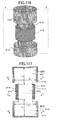
- FIG. 1 is a bird's-eye view showing a semiconductor device according to a first embodiment of the present invention.
- FIG. 2 is a schematic sectional view taken along the cutting-plane line a-a' in FIG. 1 .
- FIG. 3 is a schematic sectional view taken along the cutting-plane line b-b' in FIG. 2 .
- FIG 4 is a schematic sectional view taken along the cutting-plane line c-c' in FIG. 2 .
- FIG. 5 is a schematic sectional view taken along the cutting-plane line d-d' in FIG. 2 .
- the semiconductor device comprises a first-conductive type third silicon pillar 830, a first dielectric 310 surrounding a side surface of the third silicon pillar 830, a gate 210 surrounding the dielectric 310, a first silicon pillar 810 provided underneath the third silicon pillar 830, and a second silicon pillar 820 provided on a top of the third silicon pillar 830, wherein: the first silicon pillar 810 has a second-conductive type high-concentration impurity region 610 (i.e., concave drain diffusion layer 610) formed in a surface thereof except at least a part of a contact surface region with the third silicon pillar 830, and a first-conductive type impurity region 510 formed therein and surrounded by the second-conductive type high-concentration impurity region 610; and the second silicon pillar 820 has a second-conductive type high-concentration impurity region 710 (i.e., concave source diffusion layer 710) formed in a surface thereof except at least a part of a contact
- an outer peripheral surface except an upper surface thereof is covered by an inner surface of the drain diffusion layer 610 having an angular-U shape in vertical section.
- an outer peripheral surface except a lower surface thereof is covered by an inner surface of the source diffusion layer 710 having an inversed angular-U shape in vertical section.
- each of the first-conductive type impurity region 510 of the first silicon pillar 810 and the first-conductive type impurity region 520 of the second silicon pillar 820 has a sufficiently-large area.
- a diameter Td and a height (height dimension) Ld of the first-conductive type impurity region 510, and a diameter Ts and a height (height dimension) Ls of the first-conductive type impurity region 520 are sufficiently large.
- FIG. 22 shows a structure dependence of the punch-through voltage.
- the vertical axis of FIG. 22 represents the punch-through voltage Vpt.
- the term "punch-through voltage” means a voltage which is applied to a drain electrode so as to cause a drain current of 1e-7 A/um under a condition that a voltage applied to each of a gate electrode and a source electrode is zero V.
- the horizontal axis of FIG. 22 represents the height Ld of the impurity region 510 and the height Ls of the impurity region 520.
- a polygonal line 2201 indicates the simulation result on the semiconductor device according to the first embodiment
- each of two polygonal lines 2202, 2203 indicates a simulation result on a respective one of two semiconductor devices according to after-mentioned second and third embodiments of the present invention.
- a point 2200 indicates a simulation result on a conventional SGT (SGT having horizontally flat source and drain diffusion layers) as shown in FIGS. 123 and 124 .
- the simulation result illustrated in FIG. 22 indicates that, in the semiconductor device according to the first embodiment (polygonal line 2201), a higher punch-through voltage as compared with the conventional SGT (point 2200) is provided at any value of each of the heights Ls, Ld other than zero. In other words, it is proven that the semiconductor device according to the first embodiment has an SGT structure with a smaller off-leak current than that in the conventional SGT.
- FIG. 23 is a graph showing a dependence of each of the heights Ld, Ls on the gate length Lg, in the semiconductor device according to the first embodiment.
- a region A expressed by a plurality of vertical lines corresponds to a region where a Sub threshold swing is equal to or less than 90 mV/dec.
- the term "Sub threshold swing” means a gate voltage value at a sub-threshold area which changes a drain current by one decade with a drain voltage held constant.
- the gate length Lg may be set to 94 nm or more to allow the Sub threshold swing to become equal to or less than 90 mV/dec.
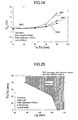
- FIG. 24 is a graph showing a dependence of the punch-through voltage on each of the diameters Ts, Td, in the semiconductor device according to the first embodiment, by comparison with the conventional SGT.
- the vertical axis represents the punch-through voltage
- the horizontal axis represents the diameter Td of the impurity region 510 and the diameter Ts of the impurity region 520.
- a polygonal line 2401 indicates the simulation result on the semiconductor device according to the first embodiment
- each of two polygonal lines 2402, 2403 indicates the simulation result on a respective one of the two semiconductor devices according to the after-mentioned second and third embodiments.
- a point 2400 indicates the simulation result on the conventional SGT (SGT having horizontally flat source and drain diffusion layers) as shown in FIGS. 123 and 124 .
- the semiconductor device according to the first embodiment has an SGT structure with a smaller off-leak current than that in the conventional SGT (point 2400).
- FIG. 25 shows a dependence of each of the diameters Td, Ts on the gate length Lg, in the semiconductor device according to the first embodiment.
- a region B expressed by a plurality of vertical lines corresponds to the region where the Sub threshold swing is equal to or less than 90 mV/dec.
- the gate length Lg may be set to 94 nm or more to allow the Sub threshold swing to become equal to or less than 90 mV/dec.
- a depletion layer in the entire silicon pillar is divided, into a depletion layer 2270 extending from the gate, a depletion layer 2230 extending from a base portion of the concave source diffusion layer, a depletion layer 2240 extending from a side portion of the concave source diffusion layer, a diffusion layer 2210 extending from a base portion of the concave drain diffusion layer, and a depletion layer 2220 extending from a side portion of the concave drain diffusion layer.
- a depth of the depletion layer 2230 extending from the base portion of the concave source diffusion layer is Ts/4.
- the height Ls is greater than the depth "Ts/4" of the depletion layer. In other words, it is essential to satisfy the following relation (1-1): Ls > Ts 4
- a depth of the depletion layer 2220 extending from the base portion of the concave drain diffusion layer is Td/4.
- FIG. 8 is a schematic bird's-eye view of a transistor as a semiconductor device of the present invention, wherein the first-conductive type impurity region 510 of the first silicon pillar 810 in the first embodiment is also formed as a second-conductive type high-concentration impurity region, in addition to the second-conductive type high-concentration impurity region 610 of the first silicon pillar 810.
- FIG. 9 is a schematic sectional view taken along the cutting-plane line a-a' in FIG. 8
- FIG. 10 is a schematic sectional view taken along the cutting-plane line b-b' in FIG. 9
- FIG. 11 is a schematic sectional view taken along the cutting-plane line c-c' in FIG. 9
- FIG. 12 is a schematic sectional view taken along the cutting-plane line d-d' in FIG. 9 .
- a first-conductive type impurity region 520 provided in a second silicon pillar 820 has a sufficiently-large area. In other words, it is desirable that a diameter Ts and a height Ls of the first-conductive type impurity region 520 are sufficiently large.
- FIG. 22 shows a structure dependence of the punch-through voltage.
- the vertical axis of FIG. 22 represents the punch-through voltage (Vpt) which is a voltage applied to a drain electrode so as to cause a drain current of le-7A/um under a condition that a voltage applied to each of a gate electrode and a source electrode is zero V.
- the horizontal axis represents the height Ls which varies according to a change in shape of a concave source diffusion layer.
- a higher punch-through voltage as compared with the horizontally flat source/drain diffusion layer-type SGT structure is provided at any value of the height Ls other than zero, which is proven that the SGT structure has a small off-leak current.
- FIG. 24 shows a dependence of the punch-through voltage on Ts, Td which varies according to a change in shape of the concave source diffusion layer.
- Ts concave source diffusion layer-type SGT structure
- FIG. 24 shows a higher punch-through voltage as compared with the horizontally flat source/drain diffusion layer-type SGT structure (conventional SGT structure indicated by the point 2400) is also provided at any value of the diameter Ts other than zero, which is proven that the SGT structure has a small off-leak current.
- a depletion layer in the entire silicon pillar is divided into four depletion layers extending from respective ones of the gate, a base portion and a side portion of the concave source diffusion layer, and a drain diffusion layer.
- a depth of the depletion layer 2230 extending from the base portion of the concave source diffusion layer is Ts/4.
- the height Ls is greater than the depth "Ts/4" of the depletion layer. In other words, it is essential to satisfy the following relation (2-1): Ls > Ts 4
- Ls is required to satisfy the following relation (2-3): tan ⁇ 36 ⁇ Tspace - Lg + Ljs + Ljd > Ls
- FIG. 15 is a schematic bird's-eye view of a transistor as a semiconductor device of the present invention, wherein the first-conductive type impurity region 520 of the second silicon pillar 820 in the first embodiment is also formed as a second-conductive type high-concentration impurity region, in addition to the second-conductive type high-concentration impurity region 710 of the second silicon pillar 820.
- FIG. 16 is a schematic sectional view taken along the cutting-plane line a-a' in FIG. 15
- FIG. 17 is a schematic sectional view taken along the cutting-plane line b-b' in FIG. 16
- FIG. 18 is a schematic sectional view taken along the cutting-plane line c-c' in FIG. 16
- FIG. 19 is a schematic sectional view taken along the cutting-plane line d-d' in FIG. 16 .
- a first-conductive type impurity region 510 provided in a first silicon pillar 810 has a sufficiently-large area. In other words, it is desirable that a diameter Td and a height Ld of the first-conductive type impurity region 510 are sufficiently large.
- FIG. 22 shows a structure dependence of the punch-through voltage.
- the vertical axis of FIG. 22 represents the punch-through voltage which is a voltage applied to a drain electrode so as to cause a drain current of 1e-7A/um under a condition that a voltage applied to each of a gate electrode and a source electrode is zero V.
- the horizontal axis represents the height Ld which varies according to a change in shape of a concave drain diffusion layer.
- a higher punch-through voltage as compared with the horizontally flat source/drain diffusion layer-type SGT structure is provided at any value of the height Ld other than zero, which is proven that the SGT structure has a small off-leak current.
- FIG 24 shows a dependence of the punch-through voltage on the diameter Td which varies according to a change in shape of the concave drain diffusion layer.
- a higher punch-through voltage as compared with the horizontally flat source/drain diffusion layer-type SGT structure is also provided at any value of the diameter Td other than zero, which is proven that the SGT structure has a small off-leak current.
- a depletion layer in the entire silicon pillar is divided into four depletion layers extending from respective ones of the gate, a source diffusion layer, and a base portion and a side portion of the concave drain diffusion layer.
- a depth of the depletion layer 2210 extending from the base portion of the concave drain diffusion layer is Td/4.
- the height Ld is greater than the depth "Td/4" of the depletion layer. In other words, it is essential to satisfy the following relation (3-1): Ld > Td 4
- FIG. 26 is a schematic bird's-eye view of a transistor as a semiconductor device of the present invention, wherein the third silicon pillar 830 in the first embodiment is formed as a high resistance region, instead of a first-conductive type impurity region, and each of the first-conductive type impurity region of the first silicon pillar 810 and the first-conductive type impurity region of the second silicon pillar 820 in the first embodiment is formed as a high resistance region.
- FIG. 27 is a schematic sectional view taken along the cutting-plane line a-a' in FIG. 26
- FIG. 28 is a schematic sectional view taken along the cutting-plane line b-b' in FIG. 27 .
- each of a high resistance region 1010 provided in a first silicon pillar 810, and a high resistance region 1020 provided in a second silicon pillar 820 has a sufficiently-large area.
- a diameter Td and a height Ld of the high resistance region 1010, and a diameter Ts and a height Ls of the high resistance region 1020 are sufficiently large.
- FIG. 41 shows a structure dependence of the punch-through voltage.
- the vertical axis of FIG. 41 represents the punch-through voltage Vpt which is a voltage applied to a drain electrode so as to cause a drain current of 1e-7A/um under a condition that a voltage applied to each of a gate electrode and a source electrode is zero V.
- the horizontal axis represents the heights Ls, Ld which vary according to a change in shape of respective ones of a concave source diffusion layer and a concave drain diffusion layer.
- Ls, Ld which vary according to a change in shape of respective ones of a concave source diffusion layer and a concave drain diffusion layer.
- FIG. 41 in the concave source/drain diffusion layer-type SGT structure (polygonal line 4101), a higher punch-through voltage as compared with the horizontally flat source/drain diffusion layer-type SGT structure (conventional SGT structure indicated by the point 4100) is provided at any value of each of the heights Ls, Ld other than zero, which is proven that the SGT structure has a small off-leak current.
- FIG. 17 shows a dependence of each of the heights Ls, Ld on the gate length Lg.
- FIG. 42 shows a dependence of the punch-through voltage (vertical axis) on each of the diameters Ts, Td (horizontal axis) which vary according to a change in shape of respective ones of the concave source diffusion layer and the concave drain diffusion layer.
- a higher punch-through voltage as compared with the horizontally flat source/drain diffusion layer-type SGT structure is also provided at any value of each of the diameters Ts, Td other than zero, which is proven that the SGT structure has a small off-leak current.
- FIG. 31 is a schematic bird's-eye view of a transistor as a semiconductor device of the present invention, wherein the silicon pillar 830 in the second embodiment is formed as a high resistance region, instead of a first-conductive type impurity region, and the first-conductive type impurity region of the silicon pillar 820 in the second embodiment is formed as a high resistance region.
- FIG. 32 is a schematic sectional view taken along the cutting-plane line a-a' in FIG. 31
- FIG. 33 is a schematic sectional view taken along the cutting-plane line b-b' in FIG. 32 .
- FIG. 34 is a schematic sectional view taken along the cutting-plane line c-c' in FIG. 32
- a high resistance region 520 provided in a second silicon pillar 820 has a sufficiently-large area. In other words, it is desirable that a diameter Ts and a height Ls are sufficiently large.
- FIG. 41 shows a structure dependence of the punch-through voltage.
- the vertical axis of FIG. 41 represents the punch-through voltage Vpt which is a voltage applied to a drain electrode so as to cause a drain current of 1e-7A/um under a condition that a voltage applied to each of a gate electrode and a source electrode is zero V.
- the horizontal axis represents the height Ls which varies according to a change in shape of a concave source diffusion layer.
- a higher punch-through voltage as compared with the horizontally flat source/drain diffusion layer-type SGT structure is provided at any value of the height Ls other than zero, which is proven that the SGT structure has a small off-leak current.
- FIG. 42 shows a dependence of the punch-through voltage on the Ts and Td which varies according to a change in shape of the concave source diffusion layer.
- a higher punch-through voltage as compared with the horizontally flat source/drain diffusion layer-type SGT structure is also provided at any value of the diameter Ts other than zero, which is proven that the SGT structure has a small off-leak current.
- FIG. 36 is a schematic bird's-eye view of a transistor as a semiconductor device of the present invention, wherein the silicon pillar 830 in the third embodiment is formed as a high resistance region, instead of a first-conductive type impurity region, and the first-conductive type impurity region of the silicon pillar 810 in the third embodiment is formed as a high resistance region.
- FIG. 37 is a schematic sectional view taken along the cutting-plane line a-a' in FIG. 36
- FIG. 38 is a schematic sectional view taken along the cutting-plane line b-b' in FIG. 37
- FIG. 39 is a schematic sectional view taken along the cutting-plane line c-c' in FIG. 37
- the semiconductor device comprises a first-conductive type third silicon pillar 840, a first dielectric 310 surrounding a side surface of the third silicon pillar 840, a gate 210 surrounding the dielectric 310, a first silicon layer 810 provided underneath the third silicon pillar 840, and a second silicon pillar 820 provided on a top of the third silicon pillar 840, wherein: the first silicon pillar 810 has a second-conductive type high-concentration impurity region 610, and a high resistance region 1010 formed therein and surrounded by the second-conductive type high-concentration impurity region 610; and the second silicon pillar 820 is formed as a second-conductive type high-concentration impurity region 710.
- the high resistance region 1010 of the first silicon pillar 810 has a sufficiently-large area. In other words, it is desirable that a diameter Td and a height Ld of the high resistance region 1010 are sufficiently large.
- FIG. 41 shows a structure dependence of the punch-through voltage.
- the vertical axis of FIG. 41 represents the punch-through voltage Vpt which is a voltage applied to a drain electrode so as to cause a drain current of 1e-7A/um under a condition that a voltage applied to each of a gate electrode and a source electrode is zero V.
- the horizontal axis represents the height Ld which varies according to a change in shape of the concave drain diffusion layer.
- a higher punch-through voltage as compared with the horizontally flat source/drain diffusion layer-type SGT structure is provided at any value of the height Ld other than zero, which is proven that the SGT structure has a small off-leak current.
- FIG. 42 shows a dependence of the punch-through voltage on the diameter Td which varies according to a change in shape of the concave drain diffusion layer.
- a higher punch-through voltage as compared with the horizontally flat source/drain diffusion layer-type SGT structure is also provided at any value of the diameter Td other than zero, which is proven that the SGT structure has a small off-leak current.
- FIG 43 is a bird's-eye view showing a transistor as a semiconductor device of the present invention.
- FIG. 44 is a schematic sectional view taken along the cutting-plane line a-a' in FIG. 43
- FIG 45 is a schematic sectional view taken along the cutting-plane line b-b' in FIG. 44 .
- FIG 46 is a schematic sectional view taken along the cutting-plane line c-c' in FIG 44
- FIG. 47 is a schematic sectional view taken along the cutting-plane line d-d' in FIG. 44 .
- the semiconductor device comprises a first-conductive type first silicon pillar 830, a first dielectric 310 surrounding a side surface of the third silicon pillar 830, a gate 210 surrounding the dielectric 310, a first silicon pillar 810 provided underneath the third silicon pillar 830 to partially have a diameter greater than that of the third silicon pillar 830, and a second silicon pillar 820 provided on a top of the third silicon pillar 830 to partially have a diameter greater than that of the third silicon pillar 830, wherein: the first silicon pillar 810 has a second-conductive type high-concentration impurity region 610 formed in a surface thereof except at least a part of a contact surface region with the third silicon pillar 830, and a first-conductive type impurity region 510 formed therein and surrounded by the second-conductive type high-concentration impurity region 610; and the second silicon pillar 820 has a second-conductive type high-concentration impurity region 710 formed in a surface thereof except at least
- each of the first-conductive type impurity region 510 of the first silicon pillar 810 and the first-conductive type impurity region 520 of the second silicon pillar 820 has a sufficiently-large area.
- a diameter Td and a height Ld of the first-conductive type impurity region 510, and a diameter Ts and a height Ls of the first-conductive type impurity region 520 are sufficiently large.
- FIG. 58 shows a dependence of the punch-through voltage on each of the diameters Ts, Td which vary according to a change in shape of respective ones of the concave source diffusion layer and the concave drain diffusion layer.
- a higher punch-through voltage as compared with the horizontally flat source/drain diffusion layer-type SGT structure is provided at any value of each of the diameters Ts, Td other than zero, which is proven that the SGT structure has a small off-leak current.
- FIG. 48 is a bird's-eye view showing a transistor as a semiconductor device of the present invention.
- FIG. 49 is a schematic sectional view taken along the cutting-plane line a-a' in FIG. 48
- FIG. 50 is a schematic sectional view taken along the cutting-plane line b-b' in FIG. 48 .
- FIG. 51 is a schematic sectional view taken along the cutting-plane line c-c' in FIG. 48
- FIG. 52 is a schematic sectional view taken along the cutting-plane line d-d' in FIG 48 .
- the semiconductor device comprises a first-conductive type third silicon pillar 830, a first dielectric 310 surrounding a side surface of the third silicon pillar 830, a gate 210 surrounding the dielectric 310, a first silicon pillar 810 provided underneath the third silicon pillar 830 to partially have a diameter greater than that of the third silicon pillar 830, and a second silicon pillar 820 provided on a top of the third silicon pillar 830 to partially have a diameter greater than that of the third silicon pillar 830, wherein: the first silicon pillar 810 is formed as a second-conductive type high-concentration impurity region 610; and the second silicon pillar 820 has a second-conductive type high-concentration impurity region 710 formed in a surface thereof except at least a part of a contact surface region with the third silicon pillar 830, and a first-conductive type impurity region 520 formed therein and surrounded by the second-conductive type high-concentration impurity region 710.
- the first-conductive type impurity region 520 of the second silicon pillar 820 has a sufficiently-large area. In other words, it is desirable that a diameter Ts and a height Ls of the first-conductive type impurity region 520 are sufficiently large.
- FIG. 58 shows a dependence of the punch-through voltage on the Ts, Td which varies according to a change in shape of the concave source diffusion layer.
- a higher punch-through voltage as compared with the horizontally flat source/drain diffusion layer-type SGT structure is provided at any value of the Ts, Td other than zero, which is proven that the SGT structure has a small off-leak current.
- FIG. 53 is a bird's-eye view showing a transistor as a semiconductor device of the present invention.
- FIG. 54 is a schematic sectional view taken along the cutting-plane line a-a' in FIG. 53
- FIG. 55 is a schematic sectional view taken along the cutting-plane line b-b' in FIG. 54 .
- FIG. 56 is a schematic sectional view taken along the cutting-plane line c-c' in FIG. 54
- FIG. 57 is a schematic sectional view taken along the cutting-plane line d-d' in FIG. 54 .
- the semiconductor device comprises a first-conductive type third silicon pillar 830, a first dielectric 310 surrounding a side surface of the third silicon pillar 830, a gate 210 surrounding the dielectric 310, a first silicon pillar 810 provided underneath the third silicon pillar 830 to partially have a diameter greater than that of the third silicon pillar 830, and a second silicon pillar 820 provided on a top of the third silicon pillar 830 to partially have a diameter greater than that of the third silicon pillar 830, wherein: the first silicon pillar 810 has a second-conductive type high-concentration impurity region 610 formed in a surface thereof except at least a part of a contact surface region with the third silicon pillar 830, and a first-conductive type impurity region 510 formed therein and surrounded by the second-conductive type high-concentration impurity region 610; and the second silicon pillar 820 is formed as a second-conductive type high-concentration impurity region 710.
- the first-conductive type impurity region 510 of the first silicon pillar 810 has a sufficiently-large area. In other words, it is desirable that a diameter Td and a height Ld of the first-conductive type impurity region 510 are sufficiently large.
- FIG. 58 shows a dependence of the punch-through voltage on the Td which varies according to a change in shape of the concave drain diffusion layer.
- a higher punch-through voltage as compared with the horizontally flat source/drain diffusion layer-type SGT structure is provided at any value of the diameter Td other than zero, which is proven that the SGT structure has a small off-leak current.
- FIG. 59 is a schematic bird's-eye view of a transistor as a semiconductor device of the present invention, wherein the third silicon pillar 830 in the seventh embodiment is formed as a high resistance region, instead of a first-conductive type impurity region, and each of the first-conductive type impurity region of the first silicon pillar 810 and the first-conductive type impurity region of the second silicon pillar 820 in the seventh embodiment is formed as a high resistance region.
- FIG. 60 is a schematic sectional view taken along the cutting-plane line a-a' in FIG 59
- FIG 61 is a schematic sectional view taken along the cutting-plane line b-b' in FIG 60 .
- FIG. 62 is a schematic sectional view taken along the cutting-plane line c-c' in FIG. 60
- FIG. 63 is a schematic sectional view taken along the cutting-plane line d-d' in FIG. 60 .
- each of a high resistance region 1010 provided in a first silicon pillar 810, and a high resistance region 1020 provided in a second silicon pillar 820 has a sufficiently-large area.
- a diameter Td and a height Ld of the high resistance region 1010, and a diameter Ts and a height Ls of the high resistance region 1020 are sufficiently large.
- FIG. 74 shows a dependence of the punch-through voltage on each of the diameters Ts, Td which vary according to a change in shape of respective ones of a concave source diffusion layer and a concave drain diffusion layer.
- a higher punch-through voltage as compared with the horizontally flat source/drain diffusion layer-type SGT structure is also provided at any value of each of the diameters Ts, Td other than zero, which is proven that the SGT structure has a small off-leak current.
- FIG. 64 is a schematic bird's-eye view of a transistor as a semiconductor device of the present invention, wherein the third silicon pillar 830 in the eighth embodiment is formed as a high resistance region, instead of a first-conductive type impurity region, and the first-conductive type impurity region of the second silicon pillar 820 in the eighth embodiment is formed as a high resistance region.
- FIG. 65 is a schematic sectional view taken along the cutting-plane line a-a' in FIG. 64
- FIG. 66 is a schematic sectional view taken along the cutting-plane line b-b' in FIG. 65
- FIG. 67 is a schematic sectional view taken along the cutting-plane line c-c' in FIG. 65
- 68 is a schematic sectional view taken along the cutting-plane line d-d' in FIG. 65 .
- a high resistance region 1020 provided in a second silicon pillar 820 has a sufficiently-large area.
- a diameter Ts and a height Ls are sufficiently large.
- FIG. 74 shows a dependence of the punch-through voltage on the Ts, Td which varies according to a change in shape of a concave source diffusion layer.
- a higher punch-through voltage as compared with the horizontally flat source/drain diffusion layer-type SGT structure is also provided at any value of the Ts, Td other than zero, which is proven that the SGT structure has a small off-leak current.
- FIG. 69 is a schematic bird's-eye view of a transistor as a semiconductor device of the present invention, wherein the silicon pillar 830 in the ninth embodiment is formed as a high resistance region, instead of a first-conductive type impurity region, and the first-conductive type impurity region of the silicon pillar 810 in the ninth embodiment is formed as a high resistance region.
- FIG. 70 is a schematic sectional view taken along the cutting-plane line a-a' in FIG. 69
- FIG. 71 is a schematic sectional view taken along the cutting-plane line b-b' in FIG. 70
- FIG. 72 is a schematic sectional view taken along the cutting-plane line c-c' in FIG. 70
- FIG. 73 is a schematic sectional view taken along the cutting-plane line d-d' in FIG. 70 .
- a high resistance region 1010 provided in a first silicon pillar 810 has a sufficiently-large area. In other words, it is desirable that a diameter Td and a height Ld of the high resistance region 1010 are sufficiently large.
- FIG. 74 shows a dependence of the punch-through voltage on the diameter Td which varies according to a change in shape of a concave drain diffusion layer.
- a higher punch-through voltage as compared with the horizontally flat source/drain diffusion layer-type SGT structure is also provided at any value of the diameter Td other than zero, which is proven that the SGT structure has a small off-leak current.
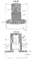
- FIG. 75 is a schematic bird's-eye view of a transistor as a semiconductor device of the present invention.
- FIG. 76 is a schematic sectional view taken along the cutting-plane line a-a' in FIG. 75 .
- FIG. 77 is a schematic sectional view taken along the cutting-plane line b-b' in FIG. 76
- FIG. 78 is a schematic sectional view taken along the cutting-plane line c-c' in FIG. 76 .
- the semiconductor device comprises a first-conductive type first silicon pillar 810 formed on a first-conductive type silicon substrate 100, a first dielectric 310 surrounding the first silicon pillar 810, a gate 210 surrounding the dielectric 310, and a second silicon pillar 820 provided on a top of the first silicon pillar 810, wherein: the silicon substrate 100 has a second-conductive type high-concentration impurity region 610 formed in a part thereof; and the second silicon layer 820 has a second-conductive type high-concentration impurity region 710 formed in a surface thereof except at least a part of a contact surface region with the third silicon pillar 810, and a first-conductive type impurity region 520 formed therein and surrounded by the second-conductive type high-concentration impurity region 710.
- the first-conductive type impurity region 520 of the second silicon pillar 820 has a sufficiently-large area. In other words, it is desirable that a diameter Ts and a height Ls of the first-conductive type impurity region 520 are sufficiently large.
- FIG. 79 shows a structure dependence of the punch-through voltage.
- the vertical axis of FIG. 79 represents the punch-through voltage Vpt which is a voltage applied to a drain electrode so as to cause a drain current of 1e-7A/um under a condition that a voltage applied to each of a gate electrode and a source electrode is zero V.
- the horizontal axis represents the height Ls which varies according to a change in shape of the concave source diffusion layer.
- a higher punch-through voltage as compared with the horizontally flat source/drain diffusion layer-type SGT structure is provided at any value of the height Ld other than zero, which is proven that the SGT structure has a small off-leak current.
- FIG. 80 shows a dependence of the punch-through voltage on the diameters Ts which varies according to a change in shape of the concave source diffusion layer.
- a higher punch-through voltage as compared with the horizontally flat source/drain diffusion layer-type SGT structure is provided at any value of the diameter Ts other than zero, which is proven that the SGT structure has a small off-leak current.
- the height Ls is greater than a depth Ts/4 of a depletion layer to suppress the punch-through effect, as with the first embodiment.
- FIG. 82 is a schematic bird's-eye view of a transistor as a semiconductor device of the present invention, wherein the third silicon pillar 830 in the embodiment is formed as a high resistance region, instead of a first-conductive type impurity region, and the first-conductive type impurity region of the second silicon pillar 820 in the embodiment is formed as a high resistance region.
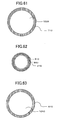
- FIG. 83 is a schematic sectional view taken along the cutting-plane line a-a' in FIG. 82 .
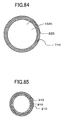
- FIG. 84 is a schematic sectional view taken along the cutting-plane line b-b' in FIG. 82
- FIG. 85 is a schematic sectional view taken along the cutting-plane line c-c' in FIG 82 .
- a high resistance region 1020 provided in a second silicon pillar 820 has a sufficiently-large area. In other words, it is desirable that a diameter Ts and a height Ls of the high resistance region 1020 are sufficiently large.
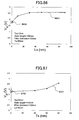
- FIG. 86 shows a structure dependence of the punch-through voltage.
- the vertical axis of FIG. 86 represents the punch-through voltage Vpt which is a voltage applied to a drain electrode so as to cause a drain current of 1e-7A/um under a condition that a voltage applied to each of a gate electrode and a source electrode is zero V.
- the horizontal axis represents the height Ls which varies according to a change in shape of a concave source diffusion layer.
- a higher punch-through voltage as compared with the horizontally flat source/drain diffusion layer-type SGT structure is provided at any value of the height Ld other than zero, which is proven that the SGT structure has a small off-leak current.
- FIG. 87 shows a dependence of the punch-through voltage on the diameter Ts which varies according to a change in shape of the concave source diffusion layer.
- a higher punch-through voltage as compared with the horizontally flat source/drain diffusion layer-type SGT structure is also provided at any value of the diameter Ts other than zero, which is proven that the SGT structure has a small off-leak current.
- FIG. 88 is a schematic bird's-eye view of a transistor as a semiconductor device of the present invention.
- FIG. 89 is a schematic sectional view taken along the cutting-plane line a-a' in FIG. 88 .
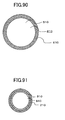
- FIG. 90 is a schematic sectional view taken along the cutting-plane line b-b' in FIG. 89
- FIG. 91 is a schematic sectional view taken along the cutting-plane line c-c' in FIG. 89 .
- the semiconductor device comprises a first-conductive type fourth silicon pillar 840 formed on a first-conductive type silicon substrate 100, a first dielectric 310 surrounding the fourth silicon pillar 810, a gate 210 surrounding the dielectric 310, and a first silicon pillar 810 provided on a top of the fourth silicon pillar 840, wherein: the silicon substrate 100 has a second-conductive type high-concentration impurity region 710 formed in a part thereof; and the first silicon layer 810 has a second-conductive type high-concentration impurity region 610 formed in a surface thereof except at least a part of a contact surface region with the fourth silicon pillar, and a first-conductive type impurity region 520 formed therein and surrounded by the second-conductive type high-concentration impurity region 610.
- the first-conductive type impurity region 510 of the first silicon pillar 810 has a sufficiently-large area. In other words, it is desirable that a diameter Ts and a height Td of the first-conductive type impurity region 510 are sufficiently large.
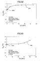
- FIG. 92 shows a structure dependence of the punch-through voltage.
- the vertical axis of FIG. 92 represents the punch-through voltage Vpt which is a voltage applied to a drain electrode so as to cause a drain current of 1e-7A/um under a condition that a voltage applied to each of a gate electrode and a source electrode is zero V.
- the horizontal axis represents the height Ls which varies according to a change in shape of the concave source diffusion layer.
- a higher punch-through voltage as compared with the horizontally flat source/drain diffusion layer-type SGT structure is provided at any value of the height Ld other than zero, which is proven that the SGT structure has a small off-leak current.
- FIG. 93 shows a dependence of the punch-through voltage on the diameters Ts which varies according to a change in shape of the concave source diffusion layer.
- a higher punch-through voltage as compared with the horizontally flat source/drain diffusion layer-type SGT structure is provided at any value of the diameter Ts other than zero, which is proven that the SGT structure has a small off-leak current.
- the height Ls is greater than a depth Ts/4 of a depletion layer to suppress the punch-through effect, as with the first embodiment.
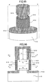
- FIG. 95 is a schematic bird's-eye view of a transistor as a semiconductor device of the present invention, wherein the third silicon pillar 830 in the embodiment is formed as a high resistance region, instead of a first-conductive type impurity region, and the first-conductive type impurity region of the second silicon pillar 820 in the embodiment is formed as a high resistance region.
- FIG. 96 is a schematic sectional view taken along the cutting-plane line a-a' in FIG. 95 .
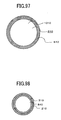
- FIG. 97 is a schematic sectional view taken along the cutting-plane line b-b' in FIG. 96
- FIG. 98 is a schematic sectional view taken along the cutting-plane line c-c' in FIG. 96 .
- a high resistance region 1010 provided in a first silicon pillar 810 has a sufficiently-large area. In other words, it is desirable that a diameter Ts and a height Ls of the high resistance region 1010 are sufficiently large.
- FIG. 99 shows a structure dependence of the punch-through voltage.
- the vertical axis of FIG. 99 represents the punch-through voltage Vpt which is a voltage applied to a drain electrode so as to cause a drain current of 1e-7A/um under a condition that a voltage applied to each of a gate electrode and a source electrode is zero V.
- the horizontal axis represents the height Ld which varies according to a change in shape of a concave source diffusion layer.
- a higher punch-through voltage as compared with the horizontally flat source/drain diffusion layer-type SGT structure is provided at any value of the height Ld other than zero, which is proven that the SGT structure has a small off-leak current.
- FIG. 100 shows a dependence of the punch-through voltage on the diameter Td which varies according to a change in shape of the concave drain diffusion layer.
- a higher punch-through voltage as compared with the horizontally flat source/drain diffusion layer-type SGT structure is also provided at any value of the diameter Ts other than zero, which is proven that the SGT structure has a small off-leak current.
- FIG. 101 is a schematic bird's-eye view of a transistor as a semiconductor device of the present invention, wherein the first-conductive type impurity region of the first silicon layer 810 in the first embodiment is formed as a second-conductive type impurity region 511 including a region having an impurity concentration of 1E18 (cm -3 ) or less, and the first-conductive type impurity region of the second silicon layer 820 in the first embodiment is formed as a second-conductive type impurity region 521 including a region having an impurity concentration of 1E18 (cm -3 ) or less.
- FIG. 102 is a schematic sectional view taken along the cutting-plane line a-a' in FIG. 101 , and FIG.
- FIG. 103 is a schematic sectional view taken along the cutting-plane line b-b' in FIG. 102 .
- FIG. 104 is a schematic sectional view taken along the cutting-plane line c-c' in FIG. 102
- FIG. 105 is a schematic sectional view taken along the cutting-plane line d-d' in FIG. 102 .
- each of the second-conductive type low-concentration impurity region 511 of the first silicon pillar 810 including a region with an impurity concentration of 1E18 (cm -3 ) or less, and the second-conductive type low-concentration impurity region 521 of the second silicon pillar 820 including a region with an impurity concentration of 1E18 (cm -3 ) or less has a sufficiently-large area.
- a diameter Td and a height Ld of the second-conductive type impurity region 511, and a diameter Ts and a height Ls of the second-conductive type impurity region 521 are sufficiently large.
- FIG. 106 is a schematic bird's-eye view of a transistor as a semiconductor device of the present invention, wherein the first-conductive type impurity region of the second silicon layer 820 in the second embodiment is formed as a second-conductive type impurity region 521 including a region having an impurity concentration of 1E18 (cm -3 ) or less.
- FIG 107 is a schematic sectional view taken along the cutting-plane line a-a' in FIG. 106
- FIG. 108 is a schematic sectional view taken along the cutting-plane line b-b' in FIG. 107
- FIG. 109 is a schematic sectional view taken along the cutting-plane line c-c' in FIG. 107
- FIG. 110 is a schematic sectional view taken along the cutting-plane line d-d' in FIG. 107 .
- the second-conductive type low-concentration impurity region 521 of the second silicon pillar 820 including a region with an impurity concentration of 1E18 (cm -3 ) or less has a sufficiently-large area.
- a diameter Ts and a height Ls are sufficiently large.
- FIG. 111 is a schematic bird's-eye view of a transistor as a semiconductor device of the present invention, wherein the first-conductive type impurity region of the silicon layer 810 in the third embodiment is formed as a second-conductive type impurity region 511 including a region having an impurity concentration of 1E18 (cm -3 ) or less.
- FIG. 112 is a schematic sectional view taken along the cutting-plane line a-a' in FIG. 111
- FIG 113 is a schematic sectional view taken along the cutting-plane line b-b' in FIG. 112 .
- FIG. 114 is a schematic sectional view taken along the cutting-plane line c-c' in FIG. 112
- FIG. 114 is a schematic sectional view taken along the cutting-plane line d-d' in FIG 112 .
- the semiconductor device comprises a first-conductive type third silicon pillar 830, a first dielectric 310 surrounding a side surface of the third silicon pillar 830, a gate 210 surrounding the dielectric 310, a first silicon layer 810 provided underneath the third silicon pillar 830, and a second silicon pillar 820 provided on a top of the third silicon pillar 830, wherein: the first silicon pillar 810 has a second-conductive type high-concentration impurity region 610, and a second-conductive type low-concentration impurity region 511 formed therein to have an impurity concentration of 1E18 (cm -3 ) or less and surrounded by the second-conductive type high-concentration impurity region 610; and the second silicon pillar 820 is formed as a second-conductive type high-concentration impurity region 710.
- the first-conductive type impurity region 511 of the first silicon pillar 810 has a sufficiently-large area. In other words, it is desirable that a diameter Ts and a height Ls are sufficiently large.
- FIG. 116 is a schematic bird's-eye view of a transistor as a semiconductor device of the present invention, wherein the first-conductive type impurity region of the first silicon layer 810 in the seventh embodiment is formed as a second-conductive type impurity region 511 including a region having an impurity concentration of 1E18 (cm -3 ) or less, and the first-conductive type impurity region of the silicon layer 820 in the seventh embodiment is formed as a second-conductive type impurity region 521.
- FIG. 117 is a schematic sectional view taken along the cutting-plane line a-a' in FIG. 116
- FIG. 118 is a schematic sectional view taken along the cutting-plane line b-b' in FIG. 117
- FIG. 118 is a schematic sectional view taken along the cutting-plane line c-c' in FIG. 117
- FIG. 119 is a schematic sectional view taken along the cutting-plane line d-d' in FIG. 117 .
- each of the second-conductive type low-concentration impurity region 511 of the first silicon pillar 810 including a region with an impurity concentration of 1E18 (cm -3 ) or less, and the second-conductive type low-concentration impurity region 521 of the second silicon pillar 820 including a region with an impurity concentration of 1E18 (cm -3 ) or less has a sufficiently-large area.
- a diameter Td and a height Ld of the second-conductive type impurity region 511, and a diameter Ts and a height Ls of the second-conductive type impurity region 521 are sufficiently large.
- FIG. 121 is a schematic bird's-eye view of a transistor as a semiconductor device of the present invention, wherein the first-conductive type impurity region of the silicon layer 820 in the eighth embodiment is formed as a second-conductive type impurity region 521 including a region having an impurity concentration of 1E18 (cm -3 ) or less.
- FIG. 122 is a schematic sectional view taken along the cutting-plane line a-a' in FIG. 121
- FIG. 123 is a schematic sectional view taken along the cutting-plane line b-b' in FIG. 122 .
- FIG. 124 is a schematic sectional view taken along the cutting-plane line c-c' in FIG. 122
- FIG. 124 is a schematic sectional view taken along the cutting-plane line d-d' in FIG. 122 .
- the second-conductive type low-concentration impurity region 2320 of the second silicon pillar 820 has a sufficiently-large area. In other words, it is desirable that a diameter Ts and a height Ls are sufficiently large.
- the second-conductive type low-concentration impurity region 521 of the second silicon pillar 820 including a region with an impurity concentration of 1E18 (cm -3 ) or less has a sufficiently-large area.
- a diameter Ts and a height Ls of the second-conductive type impurity region 521 are sufficiently large.
- FIG. 126 is a schematic bird's-eye view of a transistor as a semiconductor device of the present invention, wherein the first-conductive type impurity region of the silicon layer 810 in the ninth embodiment is formed as a second-conductive type impurity region 511 including a region having an impurity concentration of 1E18 (cm -3 ) or less.
- FIG 127 is a schematic sectional view taken along the cutting-plane line a-a' in FIG. 126
- FIG. 128 is a schematic sectional view taken along the cutting-plane line b-b' in FIG. 127 .
- FIG. 129 is a schematic sectional view taken along the cutting-plane line c-c' in FIG. 127
- FIG. 130 is a schematic sectional view taken along the cutting-plane line d-d' in FIG. 127 .
- the second-conductive type low-concentration impurity region 511 of the first silicon pillar 810 including a region with an impurity concentration of 1E18 (cm -3 ) or less has a sufficiently-large area.
- a diameter Ts and a height Ls of the second-conductive type impurity region 511 are sufficiently large.
- FIG. 131 is a schematic bird's-eye view of a transistor as a semiconductor device of the present invention, wherein the first-conductive type impurity region of the second silicon layer 820 in the fifteenth embodiment is formed as a second-conductive type impurity region 521 including a region having an impurity concentration of 1E18 (cm -3 ) or less.
- FIG. 132 is a schematic sectional view taken along the cutting-plane line a-a' in FIG. 131 .
- FIG. 133 is a schematic sectional view taken along the cutting-plane line b-b' in FIG. 132
- FIG. 134 is a schematic sectional view taken along the cutting-plane line c-c' in FIG. 132 .
- the second-conductive type low-concentration impurity region 521 of the second silicon pillar 820 including a region with an impurity concentration of 1E18 (cm -3 ) or less has a sufficiently-large area.
- a diameter Ts and a height Ls of the second-conductive type impurity region 521 are sufficiently large.
- FIG. 135 is a schematic bird's-eye view of a transistor as a semiconductor device of the present invention, wherein the first-conductive type impurity region of the first silicon layer 810 in the sixteenth embodiment is formed as a second-conductive type impurity region 511 including a region having an impurity concentration of 1E18 (cm -3 ) or less.
- FIG. 136 is a schematic sectional view taken along the cutting-plane line a-a' in FIG 135 .
- FIG. 137 is a schematic sectional view taken along the cutting-plane line b-b' in FIG. 136
- FIG. 138 is a schematic sectional view taken along the cutting-plane line c-c' in FIG. 136 .
- the second-conductive type low-concentration impurity region 511 of the first silicon pillar 810 including a region with an impurity concentration of 1E18 (cm -3 ) or less has a sufficiently-large area.
- a diameter Ts and a height Ls of the second-conductive type impurity region 511 are sufficiently large.
Landscapes
- Insulated Gate Type Field-Effect Transistor (AREA)
- Thin Film Transistor (AREA)
- Chemical & Material Sciences (AREA)
- Crystallography & Structural Chemistry (AREA)
Abstract
Description
- The present invention relates to a semiconductor device, and more specifically to a semiconductor device having a surrounding gate transistor (SGT) which is a three-dimensional semiconductor.
- Based on miniaturization, a planar transistor is used in a wide range of fields, such as computers, communication devices, measurement devices, automatic control devices and domestic devices, as a low-power consumption, low-cost, high-throughput microprocessor, ASIC or microcomputer, and a low-cost, large-capacity memory. However, the planar transistor is two-dimensionally formed on a semiconductor substrate. Specifically, in the planar transistor, a source, a gate and a drain are horizontally structured on a surface of a silicon substrate. In contrast, an SGT is formed in a structure where a source, a gate and a drain are arranged in a vertical direction with respect to a silicon substrate, wherein the gate is formed to surround a convex semiconductor layer (see, for example, the following Non-Patent
Document 1,FIG. 144 ). Thus, in the SGT, an occupancy area can be largely reduced as compared with the planar transistor.
However, in the SGT, a gate length becomes shorter along with miniaturization of ultra-large-scale integrated (ULSI) circuits, so that an off-leak current, i.e., a drain current when a voltage is applied to a drain electrode under a condition that a voltage applied to each of a gate electrode and a source electrode is zero V, becomes larger. - As means to reduce such an off-leak current, there has been known a technique of forming a source and a drain in a cup-like or concave structure, as disclosed, for example, in the following Non-Patent
Document 2 andPatent Document 1. - An SGT structure having a conventional source/drain structure as disclosed in the
Non-Patent Document 2 is shown inFIGS. 139 and140 . As is clear, particularly, fromFIG. 140 , the conventional source/drain structure has a horizontally flat distribution. Differently, in a source formed in a concave structure as shown inFIGS. 141 and142 , a potential barrier between the source and a pillar body during application of a voltage to a drain can be increased as compared with the conventional structure, to provide a higher punch-through voltage. Particularly, a much higher punch-through voltage can be provided by reducing a length X which is a depth of a source or drain. - Further, as disclosed in the
Patent Document 1, it is also studied to form each of a source and a drain in a concave structure (FIG. 143 ). -
- [Patent Document 1]
JP 2007-123415A -
- [Non-Patent Document 1] H. Takato et al., IEEE Transaction on Electron Devices, Vol. 38, No. 3, Mar. 1991, pp. 573-578
- [Non-Patent Document 2] R. Nishi, Journal C of the Institute of Electronics, Information and Communication Engineers (IEICE), Vol. J86-C, No. 2, Feb. 2003, pp. 200-201,
- The above conventional SGT structure is designed such that only a source region having a concave structure is sufficiently small, or each of a source region and a drain region has a concave structure. Practically, in a source or drain region having a concave structure, it is desirable that a region surrounded by the concave source or drain region is sufficiently large.
- The present invention has been made in view of the above circumstances, and it is an object thereof to provide a semiconductor device designed such that a source and/or a drain are formed in a concave shape to solve a problem that power consumption of an SGT is increased due to an increase in off-leak current.
- In order to achieve the above object, according to one aspect of the present invention, there is provided a semiconductor device which comprises: a first-conductive type first silicon pillar: a first dielectric surrounding a side surface of the first silicon pillar; a gate surrounding the dielectric; a second silicon pillar provided underneath the first silicon pillar; and a third silicon pillar provided on a top of the first silicon pillar, wherein: the second silicon pillar has a second-conductive type high-concentration impurity region formed in a surface thereof except at least a part of a contact surface region with the first silicon pillar, and a first-conductive type impurity region formed therein and surrounded by the second-conductive type high-concentration impurity region; and the third silicon pillar has a second-conductive type high-concentration impurity region formed in a surface thereof except at least a part of a contact surface region with the first silicon pillar, and a first-conductive type impurity region formed therein and surrounded by the second-conductive type high-concentration impurity region of the third silicon pillar, and wherein the first-conductive type impurity region of each of the second silicon pillar and the third silicon pillar has a length greater than that of a depletion layer extending from a base portion of a respective one of the second silicon pillar and the third silicon pillar.
-
-
FIG 1 is a bird's-eye view showing a semiconductor device according to a first embodiment of the present invention. -
FIG. 2 is a sectional view of the semiconductor device, taken along the cutting-plane line a-a' inFIG. 1 . -
FIG. 3 is a sectional view of the semiconductor device, taken along the cutting-plane line b-b' inFIG. 2 . -
FIG. 4 is a sectional view of the semiconductor device, taken along the cutting-plane line c-c' inFIG. 2 . -
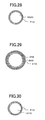
FIG. 5 is a sectional view of the semiconductor device, taken along the cutting-plane line d-d' inFIG. 2 . -
FIG. 6 is a diagram showing a depletion layer in a silicon pillar of the semiconductor device illustrated inFIG. 1 , wherein the depletion layer is divided into a plurality of elements extending from respective ones of a gate, a base portion and a side portion of a concave source diffusion layer, and a base portion and a side portion of a concave drain diffusion layer. -
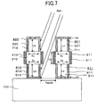
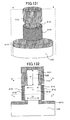
FIG. 7 is a diagram showing a process for performing ion implantation at an oblique angle to form the concave diffusion layers of the semiconductor device illustrated inFIG. 1 . -
FIG. 8 is a bird's-eye view showing a semiconductor device according to a second embodiment of the present invention. -
FIG. 9 is a sectional view of the semiconductor device, taken along the cutting-plane line a-a' inFIG. 8 . -
FIG. 10 is a sectional view of the semiconductor device, taken along the cutting-plane line b-b' inFIG. 9 . -
FIG. 11 is a sectional view of the semiconductor device, taken along the cutting-plane line c-c' inFIG. 9 . -
FIG. 12 is a sectional view of the semiconductor device, taken along the cutting-plane line d-d' inFIG. 9 . -
FIG. 13 is a diagram showing a depletion layer in a silicon pillar of the semiconductor device illustrated inFIG. 8 , wherein the depletion layer is divided into a plurality of elements extending from respective ones of a gate, a base portion and a side portion of a concave source diffusion layer, and a drain diffusion layer. -
FIG. 14 is a diagram showing a process for performing ion implantation at an oblique angle to form the concave diffusion layer of the semiconductor device illustrated inFIG. 8 . -
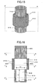
FIG. 15 is a bird's-eye view showing a semiconductor device according to a third embodiment of the present invention. -
FIG. 16 is a sectional view of the semiconductor device, taken along the cutting-plane line a-a' inFIG. 15 . -
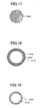
FIG. 17 is a sectional view of the semiconductor device, taken along the cutting-plane line b-b' inFIG. 16 . -
FIG. 18 is a sectional view of the semiconductor device, taken along the cutting-plane line c-c' inFIG. 16 . -
FIG. 19 is a sectional view of the semiconductor device, taken along the cutting-plane line d-d' inFIG. 16 . -
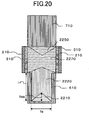
FIG. 20 is a diagram showing a depletion layer in a silicon pillar of the semiconductor device illustrated inFIG. 15 , wherein the depletion layer is divided into a plurality of elements extending from respective ones of a gate, a base portion and a side portion of a concave source diffusion layer, and a drain diffusion layer. -
FIG. 21 is a diagram showing a process for performing ion implantation at an oblique angle to form the concave diffusion layer of the semiconductor device illustrated inFIG. 15 . -
FIG. 22 is a graph showing a relationship between a punch-through voltage and a length Ls (Ld) in each of the semiconductor devices illustrated inFIGS. 1 ,8 and15 . -
FIG. 23 is graph showing a relationship between a length Ls (Ld) and a length Lg in the semiconductor device illustrated inFIG. 1 . -
FIG. 24 is a graph showing a relationship between a punch-through voltage and a diameter Ts or Td in each of the semiconductor devices illustrated inFIGS. 1 ,8 and15 . -
FIG. 25 is graph showing a relationship between a diameter Ts (Td) and a length Lg in the semiconductor device illustrated inFIG. 1 . -
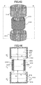
FIG. 26 is a bird's-eye view showing a semiconductor device according to a fourth embodiment of the present invention. -
FIG. 27 is a sectional view of the semiconductor device, taken along the cutting-plane line a-a' inFIG. 26 . -
FIG. 28 is a sectional view of the semiconductor device, taken along the cutting-plane line b-b' inFIG. 27 . -
FIG. 29 is a sectional view of the semiconductor device, taken along the cutting-plane line c-c' inFIG. 27 . -
FIG. 30 is a sectional view of the semiconductor device, taken along the cutting-plane line d-d' inFIG. 27 . -
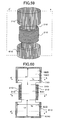
FIG. 31 is a bird's-eye view showing a semiconductor device according to a fifth embodiment of the present invention. -
FIG. 32 is a sectional view of the semiconductor device, taken along the cutting-plane line a-a' inFIG. 31 . -
FIG. 33 is a sectional view of the semiconductor device, taken along the cutting-plane line b-b' inFIG. 32 . -
FIG. 34 is a sectional view of the semiconductor device, taken along the cutting-plane line c-c' inFIG. 32 . -
FIG. 35 is a sectional view of the semiconductor device, taken along the cutting-plane line d-d' inFIG. 32 . -
FIG. 36 is a bird's-eye view showing a semiconductor device according to a sixth embodiment of the present invention. -
FIG. 37 is a sectional view of the semiconductor device, taken along the cutting-plane line a-a' inFIG. 36 . -
FIG. 38 is a sectional view of the semiconductor device, taken along the cutting-plane line b-b' inFIG. 37 . -
FIG. 39 is a sectional view of the semiconductor device, taken along the cutting-plane line c-c' inFIG. 37 . -
FIG. 40 is a sectional view of the semiconductor device, taken along the cutting-plane line d-d' inFIG. 37 . -
FIG. 41 is a graph showing a relationship between a punch-through voltage and a length Ls (Ld) in each of the semiconductor devices illustrated inFIGS. 26 ,31 and36 . -
FIG. 42 is a graph showing a relationship between a punch-through voltage and a diameter Ts (Td) in each of the semiconductor devices illustrated inFIGS. 26 ,31 and36 . -
FIG. 43 is a bird's-eye view showing a semiconductor device according to a seventh embodiment of the present invention. -
FIG. 44 is a sectional view of the semiconductor device, taken along the cutting-plane line a-a' inFIG. 43 . -
FIG. 45 is a sectional view of the semiconductor device, taken along the cutting-plane line b-b' inFIG. 44 . -
FIG. 46 is a sectional view of the semiconductor device, taken along the cutting-plane line c-c' inFIG. 44 . -
FIG. 47 is a sectional view of the semiconductor device, taken along the cutting-plane line d-d' inFIG. 44 . -
FIG. 48 is a bird's-eye view showing a semiconductor device according to an eighth embodiment of the present invention. -
FIG. 49 is a sectional view of the semiconductor device, taken along the cutting-plane line a-a' inFIG. 48 . -
FIG. 50 is a sectional view of the semiconductor device, taken along the cutting-plane line b-b' inFIG. 49 . -
FIG. 51 is a sectional view of the semiconductor device, taken along the cutting-plane line c-c' inFIG. 49 . -
FIG. 52 is a sectional view of the semiconductor device, taken along the cutting-plane line d-d' inFIG. 49 . -
FIG. 53 is a bird's-eye view showing a semiconductor device according to a ninth embodiment of the present invention. -
FIG. 54 is a sectional view of the semiconductor device, taken along the cutting-plane line a-a' inFIG. 53 . -
FIG. 55 is a sectional view of the semiconductor device, taken along the cutting-plane line b-b' inFIG. 54 . -
FIG. 56 is a sectional view of the semiconductor device, taken along the cutting-plane line c-c' inFIG. 54 . -
FIG. 57 is a sectional view of the semiconductor device, taken along the cutting-plane line d-d' inFIG. 54 . -
FIG. 58 is a graph showing a relationship between a punch-through voltage and a diameter Ts (Td) in each of the semiconductor devices illustrated inFIGS. 43 ,48 and53 . -
FIG. 59 is a bird's-eye view showing a semiconductor device according to a tenth embodiment of the present invention. -
FIG. 60 is a sectional view of the semiconductor device, taken along the cutting-plane line a-a' inFIG. 59 . -
FIG. 61 is a sectional view of the semiconductor device, taken along the cutting-plane line b-b' inFIG. 60 . -
FIG. 62 is a sectional view of the semiconductor device, taken along the cutting-plane line c-c' inFIG. 60 . -
FIG. 63 is a sectional view of the semiconductor device, taken along the cutting-plane line d-d' inFIG. 60 . -
FIG. 64 is a bird's-eye view showing a semiconductor device according to an eleventh embodiment of the present invention. -
FIG. 65 is a sectional view of the semiconductor device, taken along the cutting-plane line a-a' inFIG. 64 . -
FIG. 66 is a sectional view of the semiconductor device, taken along the cutting-plane line b-b' inFIG. 65 . -
FIG. 67 is a sectional view of the semiconductor device, taken along the cutting-plane line c-c' inFIG. 65 . -
FIG. 68 is a sectional view of the semiconductor device, taken along the cutting-plane line d-d' inFIG. 65 . -
FIG. 69 is a bird's-eye view showing a semiconductor device according to a twelfth embodiment of the present invention. -
FIG. 70 is a sectional view of the semiconductor device, taken along the cutting-plane line a-a' inFIG. 69 . -
FIG. 71 is a sectional view of the semiconductor device, taken along the cutting-plane line b-b' inFIG. 70 . -
FIG. 72 is a sectional view of the semiconductor device, taken along the cutting-plane line c-c' inFIG. 70 . -
FIG. 73 is a sectional view of the semiconductor device, taken along the cutting-plane line d-d' inFIG. 70 . -
FIG. 74 is a graph showing a relationship between a punch-through voltage and a diameter Ts (Td) in each of the semiconductor devices illustrated inFIGS. 59 ,64 and69 . -
FIG. 75 is a bird's-eye view showing a semiconductor device according to a thirteenth embodiment of the present invention. -
FIG. 76 is a sectional view of the semiconductor device, taken along the cutting-plane line a-a' inFIG. 75 . -
FIG. 77 is a sectional view of the semiconductor device, taken along the cutting-plane line b-b' inFIG. 76 . -
FIG. 78 is a sectional view of the semiconductor device, taken along the cutting-plane line c-c' inFIG. 76 . -
FIG. 79 is a graph showing a relationship between a punch-through voltage and a length Ls in the semiconductor device illustrated inFIG. 75 . -
FIG. 80 is a graph showing a relationship between a punch-through voltage and a diameter Ts (Td) in the semiconductor device illustrated inFIG. 75 . -
FIG. 81 is a diagram showing a process for performing ion implantation at an oblique angle to form a concave diffusion layer of the semiconductor device illustrated inFIG. 75 . -
FIG. 82 is a bird's-eye view showing a semiconductor device according to a fourteenth embodiment of the present invention. -
FIG. 83 is a sectional view of the semiconductor device, taken along the cutting-plane line a-a' inFIG. 82 . -
FIG. 84 is a sectional view of the semiconductor device, taken along the cutting-plane line b-b' inFIG. 83 . -
FIG. 85 is a sectional view of the semiconductor device, taken along the cutting-plane line c-c' inFIG. 83 . -
FIG. 86 is a graph showing a relationship between a punch-through voltage and Ls, Ld in the semiconductor device illustrated inFIG. 82 . -
FIG. 87 is a graph showing a relationship between a punch-through voltage and a diameter Ts (Td) in the semiconductor device illustrated inFIG. 82 . -
FIG. 88 is a bird's-eye view showing a semiconductor device according to a fifteenth embodiment of the present invention. -
FIG. 89 is a sectional view of the semiconductor device, taken along the cutting-plane line a-a' inFIG. 88 . -
FIG. 90 is a sectional view of the semiconductor device, taken along the cutting-plane line b-b' inFIG. 89 . -
FIG. 91 is a sectional view of the semiconductor device, taken along the cutting-plane line c-c' inFIG. 89 . -
FIG. 92 is a graph showing a relationship between a punch-through voltage and Ls, Ld in the semiconductor device illustrated inFIG. 88 . -
FIG. 93 is a graph showing a relationship between a punch-through voltage and a diameter Ts (Td) in the semiconductor device illustrated inFIG. 88 . -
FIG. 94 is a diagram showing a process for performing ion implantation at an oblique angle to form a concave diffusion layer of the semiconductor device illustrated inFIG. 88 . -
FIG. 95 is a bird's-eye view showing a semiconductor device according to a sixteenth embodiment of the present invention. -
FIG. 96 is a sectional view of the semiconductor device, taken along the cutting-plane line a-a' inFIG. 95 . -
FIG. 97 is a sectional view of the semiconductor device, taken along the cutting-plane line b-b' inFIG. 96 . -
FIG. 98 is a sectional view of the semiconductor device, taken along the cutting-plane line c-c' inFIG. 96 . -
FIG. 99 is a graph showing a relationship between a punch-through voltage and Ls, Ld in the semiconductor device illustrated inFIG. 95 . -
FIG. 100 is a graph showing a relationship between a punch-through voltage and a diameter Ts (Td) in the semiconductor device illustrated inFIG. 95 . -
FIG. 101 is a bird's-eye view showing a semiconductor device according to a seventeenth embodiment of the present invention. -
FIG. 102 is a sectional view of the semiconductor device, taken along the cutting-plane line a-a' inFIG. 101 . -
FIG. 103 is a sectional view of the semiconductor device, taken along the cutting-plane line b-b' inFIG. 102 . -
FIG. 104 is a sectional view of the semiconductor device, taken along the cutting-plane line c-c' inFIG. 102 . -
FIG. 105 is a sectional view of the semiconductor device, taken along the cutting-plane line d-d' inFIG. 102 . -
FIG. 106 is a bird's-eye view showing a semiconductor device according to an eighteenth embodiment of the present invention. -
FIG. 107 is a sectional view of the semiconductor device, taken along the cutting-plane line a-a' inFIG. 106 . -
FIG. 108 is a sectional view of the semiconductor device, taken along the cutting-plane line b-b' inFIG. 107 . -
FIG. 109 is a sectional view of the semiconductor device, taken along the cutting-plane line c-c' inFIG. 107 . -
FIG 110 is a sectional view of the semiconductor device, taken along the cutting-plane line d-d' inFIG. 107 . -
FIG. 111 is a bird's-eye view showing a semiconductor device according to a nineteenth embodiment of the present invention. -
FIG. 112 is a sectional view of the semiconductor device, taken along the cutting-plane line a-a' inFIG. 111 . -
FIG. 113 is a sectional view of the semiconductor device, taken along the cutting-plane line b-b' inFIG. 112 . -
FIG. 114 is a sectional view of the semiconductor device, taken along the cutting-plane line c-c' inFIG. 112 . -
FIG. 115 is a sectional view of the semiconductor device, taken along the cutting-plane line d-d' inFIG. 112 . -
FIG. 116 is a bird's-eye view showing a semiconductor device according to a twentieth embodiment of the present invention. -
FIG. 117 is a sectional view of the semiconductor device, taken along the cutting-plane line a-a' inFIG. 116 . -
FIG. 118 is a sectional view of the semiconductor device, taken along the cutting-plane line b-b' inFIG. 117 . -
FIG. 119 is a sectional view of the semiconductor device, taken along the cutting-plane line c-c' inFIG. 117 . -
FIG. 120 is a sectional view of the semiconductor device, taken along the cutting-plane line d-d' inFIG. 117 . -
FIG. 121 is a bird's-eye view showing a semiconductor device according to a twenty-first embodiment of the present invention. -
FIG. 122 is a sectional view of the semiconductor device, taken along the cutting-plane line a-a' inFIG. 121 . -
FIG. 123 is a sectional view of the semiconductor device, taken along the cutting-plane line b-b' inFIG. 122 . -
FIG. 124 is a sectional view of the semiconductor device, taken along the cutting-plane line c-c' inFIG. 122 . -
FIG. 125 is a sectional view of the semiconductor device, taken along the cutting-plane line d-d' inFIG. 122 . -
FIG. 126 is a bird's-eye view showing a semiconductor device according to a twenty-second embodiment of the present invention. -
FIG. 127 is a sectional view of the semiconductor device, taken along the cutting-plane line a-a' inFIG. 126 . -
FIG. 128 is a sectional view of the semiconductor device, taken along the cutting-plane line b-b' inFIG. 127 . -
FIG. 129 is a sectional view of the semiconductor device, taken along the cutting-plane line c-c' inFIG 127 . -
FIG. 130 is a sectional view of the semiconductor device, taken along the cutting-plane line d-d' inFIG. 127 . -
FIG. 131 is a bird's-eye view showing a semiconductor device according to a twenty-third embodiment of the present invention. -
FIG. 132 is a sectional view of the semiconductor device, taken along the cutting-plane line a-a' inFIG. 131 . -
FIG. 133 is a sectional view of the semiconductor device, taken along the cutting-plane line b-b' inFIG. 132 . -
FIG. 134 is a sectional view of the semiconductor device, taken along the cutting-plane line c-c' inFIG 132 . -
FIG. 135 is a bird's-eye view showing a semiconductor device according to a twenty-fourth embodiment of the present invention. -
FIG. 136 is a sectional view of the semiconductor device, taken along the cutting-plane line a-a' inFIG. 135 . -
FIG. 137 is a sectional view of the semiconductor device, taken along the cutting-plane line b-b' inFIG. 136 . -
FIG. 138 is a sectional view of the semiconductor device, taken along the cutting-plane line c-c' inFIG. 136 . -
FIG. 139 is a perspective view showing a structure of one example of a conventional SGT. -
FIG. 140 is a sectional view showing the structure of the conventional SGT. -
FIG. 141 is a perspective view showing a structure of another example of the conventional SGT. -
FIG. 142 is a sectional view showing the structure of the conventional SGT. -
FIG. 143 is a perspective view showing a structure of yet another example of the conventional SGT. -
FIG. 144 is a perspective view showing a structure of still another example of the conventional SGT. - With reference to the drawings, a semiconductor device of the present invention will now be specifically described.
-
FIG. 1 is a bird's-eye view showing a semiconductor device according to a first embodiment of the present invention.FIG. 2 is a schematic sectional view taken along the cutting-plane line a-a' inFIG. 1 .FIG. 3 is a schematic sectional view taken along the cutting-plane line b-b' inFIG. 2 .FIG 4 is a schematic sectional view taken along the cutting-plane line c-c' inFIG. 2 .FIG. 5 is a schematic sectional view taken along the cutting-plane line d-d' inFIG. 2 . - The semiconductor device according to the first embodiment comprises a first-conductive type
third silicon pillar 830, afirst dielectric 310 surrounding a side surface of thethird silicon pillar 830, agate 210 surrounding the dielectric 310, afirst silicon pillar 810 provided underneath thethird silicon pillar 830, and asecond silicon pillar 820 provided on a top of thethird silicon pillar 830, wherein: thefirst silicon pillar 810 has a second-conductive type high-concentration impurity region 610 (i.e., concave drain diffusion layer 610) formed in a surface thereof except at least a part of a contact surface region with thethird silicon pillar 830, and a first-conductivetype impurity region 510 formed therein and surrounded by the second-conductive type high-concentration impurity region 610; and thesecond silicon pillar 820 has a second-conductive type high-concentration impurity region 710 (i.e., concave source diffusion layer 710) formed in a surface thereof except at least a part of a contact surface region with thethird silicon pillar 830, and a first-conductivetype impurity region 520 formed therein and surrounded by the second-conductive type high-concentration impurity region 710. - In this configuration, as for the
impurity region 510 of thefirst silicon pillar 810 having a circular columnar shape, an outer peripheral surface except an upper surface thereof is covered by an inner surface of thedrain diffusion layer 610 having an angular-U shape in vertical section. Similarly, as for theimpurity region 520 of thesecond silicon pillar 820 having a circular columnar shape, an outer peripheral surface except a lower surface thereof is covered by an inner surface of thesource diffusion layer 710 having an inversed angular-U shape in vertical section. - In the first embodiment, in view of providing a higher punch-through voltage, it is desirable that each of the first-conductive
type impurity region 510 of thefirst silicon pillar 810 and the first-conductivetype impurity region 520 of thesecond silicon pillar 820 has a sufficiently-large area. In other words, it is desirable that a diameter Td and a height (height dimension) Ld of the first-conductivetype impurity region 510, and a diameter Ts and a height (height dimension) Ls of the first-conductivetype impurity region 520, are sufficiently large. - As a specific example, assuming a structure in which: a length of the
gate 210 is 100 nm; a film thickness of the gate dielectric is 2 nm; a diameter of thefirst silicon pillar 810 is 100 nm; a height (height dimension) of each of thesecond silicon pillar 820 and thethird silicon pillar 830 is 100 nm; and the diameter Td of theimpurity region 510 and the diameter Ts of theimpurity region 520 is fixed to 80 nm, a simulation was performed. As a simulation result on this structure,FIG. 22 shows a structure dependence of the punch-through voltage. - The vertical axis of
FIG. 22 represents the punch-through voltage Vpt. As used herein, the term "punch-through voltage" means a voltage which is applied to a drain electrode so as to cause a drain current of 1e-7 A/um under a condition that a voltage applied to each of a gate electrode and a source electrode is zero V. The horizontal axis ofFIG. 22 represents the height Ld of theimpurity region 510 and the height Ls of theimpurity region 520. Thus,FIG. 22 shows how the punch-through voltage is changed when each of the height Ld of theimpurity region 510 and the height Ls of theimpurity region 520 is changed, i.e., shows a dependence of the punch-through voltage on each of the heights Ld, Ls. InFIG. 22 , apolygonal line 2201 indicates the simulation result on the semiconductor device according to the first embodiment, and each of twopolygonal lines point 2200 indicates a simulation result on a conventional SGT (SGT having horizontally flat source and drain diffusion layers) as shown inFIGS. 123 and 124 . - The simulation result illustrated in
FIG. 22 indicates that, in the semiconductor device according to the first embodiment (polygonal line 2201), a higher punch-through voltage as compared with the conventional SGT (point 2200) is provided at any value of each of the heights Ls, Ld other than zero. In other words, it is proven that the semiconductor device according to the first embodiment has an SGT structure with a smaller off-leak current than that in the conventional SGT. -
FIG. 23 is a graph showing a dependence of each of the heights Ld, Ls on the gate length Lg, in the semiconductor device according to the first embodiment. InFIG. 23 , a region A expressed by a plurality of vertical lines corresponds to a region where a Sub threshold swing is equal to or less than 90 mV/dec. As used herein, the term "Sub threshold swing" means a gate voltage value at a sub-threshold area which changes a drain current by one decade with a drain voltage held constant. - As is clear from
FIG. 23 , in the conventional SGT (having a SGT structure with horizontally flat source and drain diffusion layers) where Ls = Ld = zero, it is necessary to set the gate length Lg to 102 nm or more, in order to allow the Sub threshold swing to fall within the region where it is equal to or less than 90 mV/dec. In contrast, in the semiconductor device according to the first embodiment, for example, as long as each of the heights Ls, Ld is equal to or greater than 50 nm, the gate length Lg may be set to 94 nm or more to allow the Sub threshold swing to become equal to or less than 90 mV/dec. -
FIG. 24 is a graph showing a dependence of the punch-through voltage on each of the diameters Ts, Td, in the semiconductor device according to the first embodiment, by comparison with the conventional SGT. InFIG. 24 , the vertical axis represents the punch-through voltage, and the horizontal axis represents the diameter Td of theimpurity region 510 and the diameter Ts of theimpurity region 520. InFIG. 24 , apolygonal line 2401 indicates the simulation result on the semiconductor device according to the first embodiment, and each of twopolygonal lines point 2400 indicates the simulation result on the conventional SGT (SGT having horizontally flat source and drain diffusion layers) as shown inFIGS. 123 and 124 . - As is clear from
FIG. 24 , in the semiconductor device according to the first embodiment, a higher punch-through voltage is provided at any value of each of the diameters Ts, Td other than zero. In other words, it is proven that the semiconductor device according to the first embodiment (polygonal line 2401) has an SGT structure with a smaller off-leak current than that in the conventional SGT (point 2400). -
FIG. 25 shows a dependence of each of the diameters Td, Ts on the gate length Lg, in the semiconductor device according to the first embodiment. InFIG. 25 , a region B expressed by a plurality of vertical lines corresponds to the region where the Sub threshold swing is equal to or less than 90 mV/dec. - As is clear from
FIG. 25 , in the conventional SGT (having a SGT structure with horizontally flat source and drain diffusion layers) where Ts = Td = zero, it is necessary to set the gate length Lg to 107 nm or more, in order to allow the Sub threshold swing to fall within the region where it is equal to or less than 90 mV/dec. In contrast, in the semiconductor device according to the first embodiment, for example, as long as each of the heights Ls, Ld is equal to or greater than 80 nm, the gate length Lg may be set to 94 nm or more to allow the Sub threshold swing to become equal to or less than 90 mV/dec. - The following discussion will be made based on a structure illustrated in
FIG. 6 to show a preferred value of each of the diameter Td and the height Ld of theimpurity region 510 and the diameter Ts and the height Ls of theimpurity region 520. In a complete depletion-type SGT, a depletion layer in the entire silicon pillar is divided, into adepletion layer 2270 extending from the gate, adepletion layer 2230 extending from a base portion of the concave source diffusion layer, adepletion layer 2240 extending from a side portion of the concave source diffusion layer, adiffusion layer 2210 extending from a base portion of the concave drain diffusion layer, and adepletion layer 2220 extending from a side portion of the concave drain diffusion layer. When an applied voltage is zero V, a depth of thedepletion layer 2230 extending from the base portion of the concave source diffusion layer is Ts/4. Thus, as a prerequisite to suppressing a punch-through effect due to contact between thedepletion layer 2230 extending from the base portion of the concave source diffusion layer and each of thedepletion layers 
- Similarly, a depth of the
depletion layer 2220 extending from the base portion of the concave drain diffusion layer is Td/4. Thus, as a prerequisite to suppressing a punch-through effect due to contact between thedepletion layer 2210 extending from the base portion of the concave drain diffusion layer and each of thedepletion layers 
- Further, in a process for making the concave diffusion layer-type SGT structure illustrated in
FIG. 2 , it is necessary to perform ion implantation at an oblique angle as shown inFIG. 7 so as to form the concave diffusion layers. During the ion implantation, for example, when As+ is implanted into an NMOSFET, a silicon pillar of an NMOSFET adjacent to the target NMOSFET is likely to disturb the ion implantation. Thus, it is essential to satisfy the following relation (1-3):
- , wherein:Ld is a height of the first-conductive
type impurity region 510; - Ls is a height of the first-conductive
type impurity region 520; - Lg is a length of the gate;
- Ljd is a depth of the second-conductive type high-
concentration impurity region 610; - Ljs is a depth of the second-conductive type high-concentration impurity region 620; and
- Tspace is a distance between silicon pillars of adjacent two SGTs.
- Thus, based on the relation (1-3), (Ls + Ld) is required to satisfy the following relation (1-4):

-
FIG. 8 is a schematic bird's-eye view of a transistor as a semiconductor device of the present invention, wherein the first-conductivetype impurity region 510 of thefirst silicon pillar 810 in the first embodiment is also formed as a second-conductive type high-concentration impurity region, in addition to the second-conductive type high-concentration impurity region 610 of thefirst silicon pillar 810.FIG. 9 is a schematic sectional view taken along the cutting-plane line a-a' inFIG. 8 , andFIG. 10 is a schematic sectional view taken along the cutting-plane line b-b' inFIG. 9 .FIG. 11 is a schematic sectional view taken along the cutting-plane line c-c' inFIG. 9 , andFIG. 12 is a schematic sectional view taken along the cutting-plane line d-d' inFIG. 9 . - In the second embodiment, in view of providing a higher punch-through voltage, it is desirable that a first-conductive
type impurity region 520 provided in asecond silicon pillar 820 has a sufficiently-large area. In other words, it is desirable that a diameter Ts and a height Ls of the first-conductivetype impurity region 520 are sufficiently large. - Specifically, assuming a structure in which: a length of a
gate 210 is 100 nm; a film thickness of a gate dielectric is 2 nm; a diameter of a first silicon pillar is 100 nm; and a height of each of thesecond silicon pillar 820 and athird silicon pillar 830 is 100 nm, a simulation was performed. As a simulation result on this structure,FIG. 22 shows a structure dependence of the punch-through voltage. The vertical axis ofFIG. 22 represents the punch-through voltage (Vpt) which is a voltage applied to a drain electrode so as to cause a drain current of le-7A/um under a condition that a voltage applied to each of a gate electrode and a source electrode is zero V. The horizontal axis represents the height Ls which varies according to a change in shape of a concave source diffusion layer. As see inFIG. 22 , in the concave source diffusion layer-type SGT structure (polygonal line 2202), a higher punch-through voltage as compared with the horizontally flat source/drain diffusion layer-type SGT structure (conventional SGT structure indicated by the point 2200) is provided at any value of the height Ls other than zero, which is proven that the SGT structure has a small off-leak current. -
FIG. 24 shows a dependence of the punch-through voltage on Ts, Td which varies according to a change in shape of the concave source diffusion layer. As seen inFIG. 24 , in the concave source diffusion layer-type SGT structure (polygonal line 2402), a higher punch-through voltage as compared with the horizontally flat source/drain diffusion layer-type SGT structure (conventional SGT structure indicated by the point 2400) is also provided at any value of the diameter Ts other than zero, which is proven that the SGT structure has a small off-leak current. - Based on a structure illustrated in
FIG. 13 , the following discussion will be made about the height Ls. In a complete depletion-type SGT, a depletion layer in the entire silicon pillar is divided into four depletion layers extending from respective ones of the gate, a base portion and a side portion of the concave source diffusion layer, and a drain diffusion layer. When an applied voltage is zero V, a depth of thedepletion layer 2230 extending from the base portion of the concave source diffusion layer is Ts/4. Thus, as a prerequisite to suppressing a punch-through effect due to contact between thedepletion layer 2230 extending from the base portion of the concave source diffusion layer and thedepletion layer 2250 extending from the drain diffusion layer, it is essential that the height Ls is greater than the depth "Ts/4" of the depletion layer. In other words, it is essential to satisfy the following relation (2-1):
- Further, in a process for making the concave diffusion layer-type SGT structure illustrated in
FIG. 9 , it is necessary to perform ion implantation at an oblique angle as shown inFIG. 14 so as to form the concave diffusion layer. During the ion implantation, for example, when As+ is implanted into an NMOSFET, a silicon pillar of an NMOSFET adjacent to the target NMOSFET is likely to disturb the ion implantation. Thus, it is essential to satisfy the following relation (2-2):
- , wherein:Ls is a height of the first-conductive
type impurity region 510; - Lg is a length of the gate;
- Ljd is a depth of the second-conductive type high-
concentration impurity region 610; - Ljs is a depth of the second-conductive type high-concentration impurity region 620; and
- Tspace is a distance between silicon pillars of adjacent two SGTs;
- Thus, based on the relation (2-2), Ls is required to satisfy the following relation (2-3):

-
FIG. 15 is a schematic bird's-eye view of a transistor as a semiconductor device of the present invention, wherein the first-conductivetype impurity region 520 of thesecond silicon pillar 820 in the first embodiment is also formed as a second-conductive type high-concentration impurity region, in addition to the second-conductive type high-concentration impurity region 710 of thesecond silicon pillar 820.FIG. 16 is a schematic sectional view taken along the cutting-plane line a-a' inFIG. 15 , andFIG. 17 is a schematic sectional view taken along the cutting-plane line b-b' inFIG. 16 .FIG. 18 is a schematic sectional view taken along the cutting-plane line c-c' inFIG. 16 , andFIG. 19 is a schematic sectional view taken along the cutting-plane line d-d' inFIG. 16 . - In the third embodiment, in view of providing a higher punch-through voltage, it is desirable that a first-conductive
type impurity region 510 provided in afirst silicon pillar 810 has a sufficiently-large area. In other words, it is desirable that a diameter Td and a height Ld of the first-conductivetype impurity region 510 are sufficiently large. - Specifically, assuming a structure in which: a length of a
gate 210 is 100 nm; a film thickness of agate dielectric 310 is 2 nm; a diameter of thefirst silicon pillar 810 is 100 nm; and a height of each of asecond silicon pillar 820 and athird silicon pillar 830 is 100 nm, a simulation was performed. As a simulation result on this structure,FIG. 22 shows a structure dependence of the punch-through voltage. The vertical axis ofFIG. 22 represents the punch-through voltage which is a voltage applied to a drain electrode so as to cause a drain current of 1e-7A/um under a condition that a voltage applied to each of a gate electrode and a source electrode is zero V. The horizontal axis represents the height Ld which varies according to a change in shape of a concave drain diffusion layer. As seen inFIG. 22 , in the concave drain diffusion layer-type SGT structure, a higher punch-through voltage as compared with the horizontally flat source/drain diffusion layer-type SGT structure (conventional SGT structure indicated by the point 2200) is provided at any value of the height Ld other than zero, which is proven that the SGT structure has a small off-leak current. -
FIG 24 shows a dependence of the punch-through voltage on the diameter Td which varies according to a change in shape of the concave drain diffusion layer. As seen inFIG. 24 , in the concave drain diffusion layer-type SGT structure, a higher punch-through voltage as compared with the horizontally flat source/drain diffusion layer-type SGT structure (conventional SGT structure indicated by the point 2400) is also provided at any value of the diameter Td other than zero, which is proven that the SGT structure has a small off-leak current. - Based on a structure illustrated in
FIG. 20 , the following discussion will be made about the height Ls. In a complete depletion-type SGT, a depletion layer in the entire silicon pillar is divided into four depletion layers extending from respective ones of the gate, a source diffusion layer, and a base portion and a side portion of the concave drain diffusion layer. When an applied voltage is zero V, a depth of thedepletion layer 2210 extending from the base portion of the concave drain diffusion layer is Td/4. Thus, as a prerequisite to suppressing a punch-through effect due to contact between thedepletion layer 2210 extending from the base portion of the concave drain diffusion layer and thedepletion layer 2250 extending from the source diffusion layer, it is essential that the height Ld is greater than the depth "Td/4" of the depletion layer. In other words, it is essential to satisfy the following relation (3-1):
- Further, in a process for making the concave diffusion layer-type SGT structure illustrated in
FIG. 16 , it is necessary to perform ion implantation at an oblique angle as shown inFIG. 21 so as to form the concave diffusion layer. During the ion implantation, for example, when As+ is implanted into an NMOSFET, a silicon pillar of an NMOSFET adjacent to the target NMOSFET is likely to disturb the ion implantation. Thus, it is essential to satisfy the following relation (3-2):
- , wherein:Ld is a height of the first-conductive
type impurity region 610; - Lg is a length of the gate;
- Ljd is a depth of the second-conductive type high-
concentration impurity region 610; and - Ljs is a depth of the second-conductive type high-concentration impurity region 620; and
- Tspace is a distance between silicon pillars of adjacent two SGTs.
- Thus, based on the relation (3-2), Ld is required to satisfy the following relation (3-3):

-
FIG. 26 is a schematic bird's-eye view of a transistor as a semiconductor device of the present invention, wherein thethird silicon pillar 830 in the first embodiment is formed as a high resistance region, instead of a first-conductive type impurity region, and each of the first-conductive type impurity region of thefirst silicon pillar 810 and the first-conductive type impurity region of thesecond silicon pillar 820 in the first embodiment is formed as a high resistance region.FIG. 27 is a schematic sectional view taken along the cutting-plane line a-a' inFIG. 26 , andFIG. 28 is a schematic sectional view taken along the cutting-plane line b-b' inFIG. 27 .FIG. 29 is a schematic sectional view taken along the cutting-plane line c-c' inFIG. 27 , andFIG. 30 is a schematic sectional view taken along the cutting-plane line d-d' inFIG. 27 . In the semiconductor device according to the fourth embodiment, in view of providing a higher punch-through voltage, it is desirable that each of ahigh resistance region 1010 provided in afirst silicon pillar 810, and ahigh resistance region 1020 provided in asecond silicon pillar 820, has a sufficiently-large area. In other words, it is desirable that a diameter Td and a height Ld of thehigh resistance region 1010, and a diameter Ts and a height Ls of thehigh resistance region 1020, are sufficiently large. - Specifically, assuming a structure in which: a length of a
gate 210 is 100 nm; a film thickness of a gate dielectric is 2 nm; a diameter of thefirst silicon pillar 810 is 100 nm; and a height of each of thesecond silicon pillar 820 and athird silicon pillar 840 is 100 nm, a simulation was performed. As a simulation result on this structure,FIG. 41 shows a structure dependence of the punch-through voltage. The vertical axis ofFIG. 41 represents the punch-through voltage Vpt which is a voltage applied to a drain electrode so as to cause a drain current of 1e-7A/um under a condition that a voltage applied to each of a gate electrode and a source electrode is zero V. The horizontal axis represents the heights Ls, Ld which vary according to a change in shape of respective ones of a concave source diffusion layer and a concave drain diffusion layer. As seen inFIG. 41 , in the concave source/drain diffusion layer-type SGT structure (polygonal line 4101), a higher punch-through voltage as compared with the horizontally flat source/drain diffusion layer-type SGT structure (conventional SGT structure indicated by the point 4100) is provided at any value of each of the heights Ls, Ld other than zero, which is proven that the SGT structure has a small off-leak current.FIG. 17 shows a dependence of each of the heights Ls, Ld on the gate length Lg. -
FIG. 42 shows a dependence of the punch-through voltage (vertical axis) on each of the diameters Ts, Td (horizontal axis) which vary according to a change in shape of respective ones of the concave source diffusion layer and the concave drain diffusion layer. As seen inFIG. 42 , in the concave source/drain diffusion layer-type SGT structure (polygonal line 4201), a higher punch-through voltage as compared with the horizontally flat source/drain diffusion layer-type SGT structure (conventional SGT structure indicated by the point 4200) is also provided at any value of each of the diameters Ts, Td other than zero, which is proven that the SGT structure has a small off-leak current. - In the fourth embodiment, as with the first embodiment, it is desirable to satisfy the following relations (4-1) and (4-2) to provide a higher punch-through voltage:


- Further, in the fourth embodiment, it is necessary to satisfy the following relation (4-3), as with the first embodiment, to prevent a silicon pillar of a MOSFET adjacent to a target MOSFET from disturbing ion implantation into the target MOSFET:

-
FIG. 31 is a schematic bird's-eye view of a transistor as a semiconductor device of the present invention, wherein thesilicon pillar 830 in the second embodiment is formed as a high resistance region, instead of a first-conductive type impurity region, and the first-conductive type impurity region of thesilicon pillar 820 in the second embodiment is formed as a high resistance region.FIG. 32 is a schematic sectional view taken along the cutting-plane line a-a' inFIG. 31 , andFIG. 33 is a schematic sectional view taken along the cutting-plane line b-b' inFIG. 32 .FIG. 34 is a schematic sectional view taken along the cutting-plane line c-c' inFIG. 32 , andFIG. 35 is a schematic sectional view taken along the cutting-plane line d-d' inFIG. 32 . In the fifth embodiment, in view of providing a higher punch-through voltage, it is desirable that ahigh resistance region 520 provided in asecond silicon pillar 820 has a sufficiently-large area. In other words, it is desirable that a diameter Ts and a height Ls are sufficiently large. - Specifically, assuming a structure in which: a length of a
gate 210 is 100 nm; a film thickness of a gate dielectric is 2 nm; a diameter of afirst silicon pillar 810 is 100 nm; and a height of each of thesecond silicon pillar 820 and athird silicon pillar 840 is 100 nm, a simulation was performed. As a simulation result on this structure,FIG. 41 shows a structure dependence of the punch-through voltage. The vertical axis ofFIG. 41 represents the punch-through voltage Vpt which is a voltage applied to a drain electrode so as to cause a drain current of 1e-7A/um under a condition that a voltage applied to each of a gate electrode and a source electrode is zero V. The horizontal axis represents the height Ls which varies according to a change in shape of a concave source diffusion layer. As seen inFIG. 41 , in the concave source diffusion layer-type SGT structure (polygonal line 4102), a higher punch-through voltage as compared with the horizontally flat source/drain diffusion layer-type SGT structure (conventional SGT structure indicated by the point 4100) is provided at any value of the height Ls other than zero, which is proven that the SGT structure has a small off-leak current. -
FIG. 42 shows a dependence of the punch-through voltage on the Ts and Td which varies according to a change in shape of the concave source diffusion layer. As seen inFIG. 42 , in the concave source diffusion layer-type SGT structure (polygonal line 4202), a higher punch-through voltage as compared with the horizontally flat source/drain diffusion layer-type SGT structure (conventional SGT structure indicated by the point 4200) is also provided at any value of the diameter Ts other than zero, which is proven that the SGT structure has a small off-leak current. - In the fifth embodiment, as with the second embodiment, it is desirable to satisfy the following relation (5-1) to provide a higher punch-through voltage:

- Further, in the fifth embodiment, it is necessary to satisfy the following relation (5-2), as with the second embodiment, to prevent a silicon pillar of a MOSFET adjacent to a target MOSFET from disturbing ion implantation into the target MOSFET:

-
FIG. 36 is a schematic bird's-eye view of a transistor as a semiconductor device of the present invention, wherein thesilicon pillar 830 in the third embodiment is formed as a high resistance region, instead of a first-conductive type impurity region, and the first-conductive type impurity region of thesilicon pillar 810 in the third embodiment is formed as a high resistance region.FIG. 37 is a schematic sectional view taken along the cutting-plane line a-a' inFIG. 36 , andFIG. 38 is a schematic sectional view taken along the cutting-plane line b-b' inFIG. 37 .FIG. 39 is a schematic sectional view taken along the cutting-plane line c-c' inFIG. 37 , andFIG. 40 is a schematic sectional view taken along the cutting-plane line d-d' inFIG 37 . The semiconductor device according to the sixth embodiment comprises a first-conductive typethird silicon pillar 840, afirst dielectric 310 surrounding a side surface of thethird silicon pillar 840, agate 210 surrounding the dielectric 310, afirst silicon layer 810 provided underneath thethird silicon pillar 840, and asecond silicon pillar 820 provided on a top of thethird silicon pillar 840, wherein: thefirst silicon pillar 810 has a second-conductive type high-concentration impurity region 610, and ahigh resistance region 1010 formed therein and surrounded by the second-conductive type high-concentration impurity region 610; and thesecond silicon pillar 820 is formed as a second-conductive type high-concentration impurity region 710. - In the sixth embodiment, in view of providing a higher punch-through voltage, it is desirable that the
high resistance region 1010 of thefirst silicon pillar 810 has a sufficiently-large area. In other words, it is desirable that a diameter Td and a height Ld of thehigh resistance region 1010 are sufficiently large. - Specifically, assuming a structure in which: a length of the
gate 210 is 100 nm; a film thickness of the gate dielectric is 2 nm; a diameter of thefirst silicon pillar 810 is 100 nm; and a height of each of thesecond silicon pillar 820 and thethird silicon pillar 840 is 100 nm, a simulation was performed. As a simulation result on this structure,FIG. 41 shows a structure dependence of the punch-through voltage. The vertical axis ofFIG. 41 represents the punch-through voltage Vpt which is a voltage applied to a drain electrode so as to cause a drain current of 1e-7A/um under a condition that a voltage applied to each of a gate electrode and a source electrode is zero V. The horizontal axis represents the height Ld which varies according to a change in shape of the concave drain diffusion layer. As seen inFIG. 41 , in the concave drain diffusion layer-type SGT structure (polygonal line 4103), a higher punch-through voltage as compared with the horizontally flat source/drain diffusion layer-type SGT structure (conventional SGT structure indicated by the point 4100) is provided at any value of the height Ld other than zero, which is proven that the SGT structure has a small off-leak current. -
FIG. 42 shows a dependence of the punch-through voltage on the diameter Td which varies according to a change in shape of the concave drain diffusion layer. As seen inFIG. 42 , in the concave drain diffusion layer-type SGT structure (polygonal line 4203), a higher punch-through voltage as compared with the horizontally flat source/drain diffusion layer-type SGT structure (conventional SGT structure indicated by the point 4200) is also provided at any value of the diameter Td other than zero, which is proven that the SGT structure has a small off-leak current. - In the sixth embodiment, as with the third embodiment, it is desirable to satisfy the following relation (6-1) to provide a higher punch-through voltage,:

- Further, in the sixth embodiment, it is necessary to satisfy the following relation (6-2), as with the third embodiment, to prevent a silicon pillar of a MOSFET adjacent to a target MOSFET from disturbing ion implantation into the target MOSFET:

-
FIG 43 is a bird's-eye view showing a transistor as a semiconductor device of the present invention.FIG. 44 is a schematic sectional view taken along the cutting-plane line a-a' inFIG. 43 , andFIG 45 is a schematic sectional view taken along the cutting-plane line b-b' inFIG. 44 .FIG 46 is a schematic sectional view taken along the cutting-plane line c-c' inFIG 44 , andFIG. 47 is a schematic sectional view taken along the cutting-plane line d-d' inFIG. 44 . The semiconductor device according to the seventh embodiment comprises a first-conductive typefirst silicon pillar 830, afirst dielectric 310 surrounding a side surface of thethird silicon pillar 830, agate 210 surrounding the dielectric 310, afirst silicon pillar 810 provided underneath thethird silicon pillar 830 to partially have a diameter greater than that of thethird silicon pillar 830, and asecond silicon pillar 820 provided on a top of thethird silicon pillar 830 to partially have a diameter greater than that of thethird silicon pillar 830, wherein: thefirst silicon pillar 810 has a second-conductive type high-concentration impurity region 610 formed in a surface thereof except at least a part of a contact surface region with thethird silicon pillar 830, and a first-conductivetype impurity region 510 formed therein and surrounded by the second-conductive type high-concentration impurity region 610; and thesecond silicon pillar 820 has a second-conductive type high-concentration impurity region 710 formed in a surface thereof except at least a part of a contact surface region with thethird silicon pillar 830, and a first-conductivetype impurity region 520 formed therein and surrounded by the second-conductive type high-concentration impurity region 710. - In the seventh embodiment, in view of providing a higher punch-through voltage, it is desirable that each of the first-conductive
type impurity region 510 of thefirst silicon pillar 810 and the first-conductivetype impurity region 520 of thesecond silicon pillar 820 has a sufficiently-large area. In other words, it is desirable that a diameter Td and a height Ld of the first-conductivetype impurity region 510, and a diameter Ts and a height Ls of the first-conductivetype impurity region 520, are sufficiently large. - Specifically, assuming a structure in which: a length of the
gate 210 is 100 nm; a film thickness of the gate dielectric is 2 nm; a diameter of thefirst silicon pillar 810 is 100 nm; and a height of each of thesecond silicon pillar 820 and thethird silicon pillar 830 is 100 nm, a simulation was performed. As a simulation result on this structure,FIG. 58 shows a dependence of the punch-through voltage on each of the diameters Ts, Td which vary according to a change in shape of respective ones of the concave source diffusion layer and the concave drain diffusion layer. As seen inFIG. 58 , in the concave drain/source diffusion layer-type SGT structure (polygonal line 5801), a higher punch-through voltage as compared with the horizontally flat source/drain diffusion layer-type SGT structure (conventional SGT structure indicated by the point 5800) is provided at any value of each of the diameters Ts, Td other than zero, which is proven that the SGT structure has a small off-leak current. - In the seventh embodiment, as with the first embodiment, it is desirable to satisfy the following relations (7-1) and (7-2) to provide a higher punch-through voltage:


- Further, in the seventh embodiment, it is necessary to satisfy the following relation (7-3), as with the first embodiment, to prevent a silicon pillar of a MOSFET adjacent to a target MOSFET from disturbing ion implantation into the target MOSFET:

-
FIG. 48 is a bird's-eye view showing a transistor as a semiconductor device of the present invention.FIG. 49 is a schematic sectional view taken along the cutting-plane line a-a' inFIG. 48 , andFIG. 50 is a schematic sectional view taken along the cutting-plane line b-b' inFIG. 48 .FIG. 51 is a schematic sectional view taken along the cutting-plane line c-c' inFIG. 48 , andFIG. 52 is a schematic sectional view taken along the cutting-plane line d-d' inFIG 48 . The semiconductor device according to the eighth embodiment comprises a first-conductive typethird silicon pillar 830, afirst dielectric 310 surrounding a side surface of thethird silicon pillar 830, agate 210 surrounding the dielectric 310, afirst silicon pillar 810 provided underneath thethird silicon pillar 830 to partially have a diameter greater than that of thethird silicon pillar 830, and asecond silicon pillar 820 provided on a top of thethird silicon pillar 830 to partially have a diameter greater than that of thethird silicon pillar 830, wherein: thefirst silicon pillar 810 is formed as a second-conductive type high-concentration impurity region 610; and thesecond silicon pillar 820 has a second-conductive type high-concentration impurity region 710 formed in a surface thereof except at least a part of a contact surface region with thethird silicon pillar 830, and a first-conductivetype impurity region 520 formed therein and surrounded by the second-conductive type high-concentration impurity region 710. - In the eighth embodiment, in view of providing a higher punch-through voltage, it is desirable that the first-conductive
type impurity region 520 of thesecond silicon pillar 820 has a sufficiently-large area. In other words, it is desirable that a diameter Ts and a height Ls of the first-conductivetype impurity region 520 are sufficiently large. - Specifically, assuming a structure in which: a length of the
gate 210 is 100 nm; a film thickness of the gate dielectric is 2 nm; a diameter of thefirst silicon pillar 810 is 100 nm; and a height of each of thesecond silicon pillar 820 and thethird silicon pillar 830 is 100 nm, a simulation was performed. As a simulation result on this structure,FIG. 58 shows a dependence of the punch-through voltage on the Ts, Td which varies according to a change in shape of the concave source diffusion layer. As seen inFIG. 58 , in the concave source diffusion layer-type SGT structure (polygonal line 5802), a higher punch-through voltage as compared with the horizontally flat source/drain diffusion layer-type SGT structure (conventional SGT structure indicated by the point 5800) is provided at any value of the Ts, Td other than zero, which is proven that the SGT structure has a small off-leak current. - In the eighth embodiment, as with the second embodiment, it is desirable to satisfy the following relation (8-1) to provide a higher punch-through voltage:

- Further, in the eighth embodiment, it is necessary to satisfy the following relation (8-2), as with the first embodiment, to prevent a silicon pillar of a MOSFET adjacent to a target MOSFET from disturbing ion implantation into the target MOSFET:

-
FIG. 53 is a bird's-eye view showing a transistor as a semiconductor device of the present invention.FIG. 54 is a schematic sectional view taken along the cutting-plane line a-a' inFIG. 53 , andFIG. 55 is a schematic sectional view taken along the cutting-plane line b-b' inFIG. 54 .FIG. 56 is a schematic sectional view taken along the cutting-plane line c-c' inFIG. 54 , andFIG. 57 is a schematic sectional view taken along the cutting-plane line d-d' inFIG. 54 . The semiconductor device according to the ninth embodiment comprises a first-conductive typethird silicon pillar 830, afirst dielectric 310 surrounding a side surface of thethird silicon pillar 830, agate 210 surrounding the dielectric 310, afirst silicon pillar 810 provided underneath thethird silicon pillar 830 to partially have a diameter greater than that of thethird silicon pillar 830, and asecond silicon pillar 820 provided on a top of thethird silicon pillar 830 to partially have a diameter greater than that of thethird silicon pillar 830, wherein: thefirst silicon pillar 810 has a second-conductive type high-concentration impurity region 610 formed in a surface thereof except at least a part of a contact surface region with thethird silicon pillar 830, and a first-conductivetype impurity region 510 formed therein and surrounded by the second-conductive type high-concentration impurity region 610; and thesecond silicon pillar 820 is formed as a second-conductive type high-concentration impurity region 710. - In the ninth embodiment, in view of providing a higher punch-through voltage, it is desirable that the first-conductive
type impurity region 510 of thefirst silicon pillar 810 has a sufficiently-large area. In other words, it is desirable that a diameter Td and a height Ld of the first-conductivetype impurity region 510 are sufficiently large. - Specifically, assuming a structure in which: a length of the
gate 210 is 100 nm; a film thickness of the gate dielectric is 2 nm; a diameter of thefirst silicon pillar 810 is 100 nm; and a height of each of thesecond silicon pillar 820 and thethird silicon pillar 830 is 100 nm, a simulation was performed. As a simulation result on this structure,FIG. 58 shows a dependence of the punch-through voltage on the Td which varies according to a change in shape of the concave drain diffusion layer. As seen inFIG. 58 , in the concave drain diffusion layer-type SGT structure (polygonal line 5803), a higher punch-through voltage as compared with the horizontally flat source/drain diffusion layer-type SGT structure (conventional SGT structure indicated by the point 5800) is provided at any value of the diameter Td other than zero, which is proven that the SGT structure has a small off-leak current. - In the ninth embodiment, as with the third embodiment, it is desirable to satisfy the following relation (9-1) to provide a higher punch-through voltage:

- Further, in the ninth embodiment, it is necessary to satisfy the following relation (9-2), as with the first embodiment, to prevent a silicon pillar of a MOSFET adjacent to a target MOSFET from disturbing ion implantation into the target MOSFET:

-
FIG. 59 is a schematic bird's-eye view of a transistor as a semiconductor device of the present invention, wherein thethird silicon pillar 830 in the seventh embodiment is formed as a high resistance region, instead of a first-conductive type impurity region, and each of the first-conductive type impurity region of thefirst silicon pillar 810 and the first-conductive type impurity region of thesecond silicon pillar 820 in the seventh embodiment is formed as a high resistance region.FIG. 60 is a schematic sectional view taken along the cutting-plane line a-a' inFIG 59 , andFIG 61 is a schematic sectional view taken along the cutting-plane line b-b' inFIG 60 .FIG. 62 is a schematic sectional view taken along the cutting-plane line c-c' inFIG. 60 , andFIG. 63 is a schematic sectional view taken along the cutting-plane line d-d' inFIG. 60 . In the semiconductor device according to the tenth embodiment, in view of providing a higher punch-through voltage, it is desirable that each of ahigh resistance region 1010 provided in afirst silicon pillar 810, and ahigh resistance region 1020 provided in asecond silicon pillar 820, has a sufficiently-large area. In other words, it is desirable that a diameter Td and a height Ld of thehigh resistance region 1010, and a diameter Ts and a height Ls of thehigh resistance region 1020, are sufficiently large. - Specifically, assuming a structure in which: a length of a
gate 210 is 100 nm; a film thickness of a gate dielectric is 2 nm; a diameter of thefirst silicon pillar 810 is 100 nm; and a height of each of thesecond silicon pillar 820 and thethird silicon pillar 830 is 100 nm, a simulation was performed. As a simulation result on this structure,FIG. 74 shows a dependence of the punch-through voltage on each of the diameters Ts, Td which vary according to a change in shape of respective ones of a concave source diffusion layer and a concave drain diffusion layer. As seen inFIG. 74 , in the concave source/drain diffusion layer-type SGT structure (polygonal line 7401), a higher punch-through voltage as compared with the horizontally flat source/drain diffusion layer-type SGT structure (conventional SGT structure indicated by the point 7400) is also provided at any value of each of the diameters Ts, Td other than zero, which is proven that the SGT structure has a small off-leak current. - In the tenth embodiment, as with the first embodiment, it is desirable to satisfy the following relations (10-1) and (10-2) to provide a higher punch-through voltage:


- Further, in the tenth embodiment, it is necessary to satisfy the following relation (10-3), as with the first embodiment, to prevent a silicon pillar of a MOSFET adjacent to a target MOSFET from disturbing ion implantation into the target MOSFET:

-
FIG. 64 is a schematic bird's-eye view of a transistor as a semiconductor device of the present invention, wherein thethird silicon pillar 830 in the eighth embodiment is formed as a high resistance region, instead of a first-conductive type impurity region, and the first-conductive type impurity region of thesecond silicon pillar 820 in the eighth embodiment is formed as a high resistance region.FIG. 65 is a schematic sectional view taken along the cutting-plane line a-a' inFIG. 64 , andFIG. 66 is a schematic sectional view taken along the cutting-plane line b-b' inFIG. 65 .FIG. 67 is a schematic sectional view taken along the cutting-plane line c-c' inFIG. 65 , andFIG. 68 is a schematic sectional view taken along the cutting-plane line d-d' inFIG. 65 . In the eleventh embodiment, in view of providing a higher punch-through voltage, it is desirable that ahigh resistance region 1020 provided in asecond silicon pillar 820 has a sufficiently-large area. In other words, it is desirable that a diameter Ts and a height Ls are sufficiently large. - Specifically, assuming a structure in which: a length of a
gate 210 is 100 nm; a film thickness of a gate dielectric is 2 nm; a diameter of afirst silicon pillar 810 is 100 nm; and a height of each of thesecond silicon pillar 820 and athird silicon pillar 830 is 100 nm, a simulation was performed. As a simulation result on this structure,FIG. 74 shows a dependence of the punch-through voltage on the Ts, Td which varies according to a change in shape of a concave source diffusion layer. As seen inFIG. 74 , in the concave source drain diffusion layer-type SGT structure (polygonal line 7402), a higher punch-through voltage as compared with the horizontally flat source/drain diffusion layer-type SGT structure (conventional SGT structure indicated by the point 7400) is also provided at any value of the Ts, Td other than zero, which is proven that the SGT structure has a small off-leak current. - In the eleventh embodiment, as with the second embodiment, it is desirable to satisfy the following relation (11-1) to provide a higher punch-through voltage:

- Further, in the eleventh embodiment, it is necessary to satisfy the following relation (11-2), as with the first embodiment, to prevent a silicon pillar of a MOSFET adjacent to a target MOSFET from disturbing ion implantation into the target MOSFET:

-
FIG. 69 is a schematic bird's-eye view of a transistor as a semiconductor device of the present invention, wherein thesilicon pillar 830 in the ninth embodiment is formed as a high resistance region, instead of a first-conductive type impurity region, and the first-conductive type impurity region of thesilicon pillar 810 in the ninth embodiment is formed as a high resistance region.FIG. 70 is a schematic sectional view taken along the cutting-plane line a-a' inFIG. 69 , andFIG. 71 is a schematic sectional view taken along the cutting-plane line b-b' inFIG. 70 .FIG. 72 is a schematic sectional view taken along the cutting-plane line c-c' inFIG. 70 , andFIG. 73 is a schematic sectional view taken along the cutting-plane line d-d' inFIG. 70 . - In the twelfth embodiment, in view of providing a higher punch-through voltage, it is desirable that a
high resistance region 1010 provided in afirst silicon pillar 810 has a sufficiently-large area. In other words, it is desirable that a diameter Td and a height Ld of thehigh resistance region 1010 are sufficiently large. - Specifically, assuming a structure in which: a length of a
gate 210 is 100 nm; a film thickness of agate dielectric 310 is 2 nm; a diameter of thefirst silicon pillar 810 is 100 nm; and a height of each of asecond silicon pillar 820 and athird silicon pillar 840 is 100 nm, a simulation was performed. As a simulation result on this structure,FIG. 74 shows a dependence of the punch-through voltage on the diameter Td which varies according to a change in shape of a concave drain diffusion layer. As seen inFIG. 74 , in the concave source and drain diffusion layer-type SGT structures (polygonal line 7403), a higher punch-through voltage as compared with the horizontally flat source/drain diffusion layer-type SGT structure (conventional SGT structure indicated by the point 7400) is also provided at any value of the diameter Td other than zero, which is proven that the SGT structure has a small off-leak current. - In the twelfth embodiment, as with the third embodiment, it is desirable to satisfy the following relation (12-1) to provide a higher punch-through voltage,:

- Further, in the twelfth embodiment, it is necessary to satisfy the following relation (12-2), as with the third embodiment, to prevent a silicon pillar of a MOSFET adjacent to a target MOSFET from disturbing ion implantation into the target MOSFET:

-
FIG. 75 is a schematic bird's-eye view of a transistor as a semiconductor device of the present invention.FIG. 76 is a schematic sectional view taken along the cutting-plane line a-a' inFIG. 75 .FIG. 77 is a schematic sectional view taken along the cutting-plane line b-b' inFIG. 76 , andFIG. 78 is a schematic sectional view taken along the cutting-plane line c-c' inFIG. 76 . The semiconductor device according to the thirteenth embodiment comprises a first-conductive typefirst silicon pillar 810 formed on a first-conductivetype silicon substrate 100, afirst dielectric 310 surrounding thefirst silicon pillar 810, agate 210 surrounding the dielectric 310, and asecond silicon pillar 820 provided on a top of thefirst silicon pillar 810, wherein: thesilicon substrate 100 has a second-conductive type high-concentration impurity region 610 formed in a part thereof; and thesecond silicon layer 820 has a second-conductive type high-concentration impurity region 710 formed in a surface thereof except at least a part of a contact surface region with thethird silicon pillar 810, and a first-conductivetype impurity region 520 formed therein and surrounded by the second-conductive type high-concentration impurity region 710. - In the thirteenth embodiment, in view of providing a higher punch-through voltage, it is desirable that the first-conductive
type impurity region 520 of thesecond silicon pillar 820 has a sufficiently-large area. In other words, it is desirable that a diameter Ts and a height Ls of the first-conductivetype impurity region 520 are sufficiently large. - Specifically, assuming a structure in which: a length of the
gate 210 is 100 nm; a film thickness of the gate dielectric is 2 nm; and a diameter of thefirst silicon pillar 810 is 100 nm; a height of thesecond silicon pillar 820 is 100 nm, a simulation was performed. As a simulation result on this structure,FIG. 79 shows a structure dependence of the punch-through voltage. The vertical axis ofFIG. 79 represents the punch-through voltage Vpt which is a voltage applied to a drain electrode so as to cause a drain current of 1e-7A/um under a condition that a voltage applied to each of a gate electrode and a source electrode is zero V. The horizontal axis represents the height Ls which varies according to a change in shape of the concave source diffusion layer. As seen inFIG. 79 , in the concave source diffusion layer-type SGT structure (polygonal line 7901), a higher punch-through voltage as compared with the horizontally flat source/drain diffusion layer-type SGT structure (conventional SGT structure indicated by the point 7900) is provided at any value of the height Ld other than zero, which is proven that the SGT structure has a small off-leak current. -
FIG. 80 shows a dependence of the punch-through voltage on the diameters Ts which varies according to a change in shape of the concave source diffusion layer. As seen inFIG. 80 , in the concave source diffusion layer-type SGT structure (polygonal line 8001), a higher punch-through voltage as compared with the horizontally flat source/drain diffusion layer-type SGT structure (conventional SGT structure indicated by the point 8000) is provided at any value of the diameter Ts other than zero, which is proven that the SGT structure has a small off-leak current. - In the thirteenth embodiment, it is desirable that the height Ls is greater than a depth Ts/4 of a depletion layer to suppress the punch-through effect, as with the first embodiment. In other words, it is desirable to satisfy the following relation (13-1):

- Further, in a process for making the concave diffusion layer-type SGT structure illustrated in
FIG. 75 , it is necessary to perform ion implantation at an oblique angle as shown inFIG. 81 so as to form the concave diffusion layer. During the ion implantation, for example, when As+ is implanted into an NMOSFET, a silicon pillar of an NMOSFET adjacent to the target NMOSFET is likely to disturb the ion implantation. Thus, it is essential to satisfy the following relation (13-2):
- , wherein:Ls is a height of the first-conductive
type impurity region 610; - Ljs is a depth of the second-conductive type high-concentration impurity region 620; and
- Tspace is a distance between silicon pillars of adjacent two SGTs;
- Thus, based on the relation (13-2), Ls is required to satisfy the following relation (12-3):

-
FIG. 82 is a schematic bird's-eye view of a transistor as a semiconductor device of the present invention, wherein thethird silicon pillar 830 in the embodiment is formed as a high resistance region, instead of a first-conductive type impurity region, and the first-conductive type impurity region of thesecond silicon pillar 820 in the embodiment is formed as a high resistance region.FIG. 83 is a schematic sectional view taken along the cutting-plane line a-a' inFIG. 82 .FIG. 84 is a schematic sectional view taken along the cutting-plane line b-b' inFIG. 82 , andFIG. 85 is a schematic sectional view taken along the cutting-plane line c-c' inFIG 82 . - In the fourteenth embodiment, in view of providing a higher punch-through voltage, it is desirable that a
high resistance region 1020 provided in asecond silicon pillar 820 has a sufficiently-large area. In other words, it is desirable that a diameter Ts and a height Ls of thehigh resistance region 1020 are sufficiently large. - Specifically, assuming a structure in which: a length of a
gate 210 is 100 nm; a film thickness of a gate dielectric is 2 nm; a diameter of afirst silicon pillar 810 is 100 nm; and a height of thesecond silicon pillar 820 is 100 nm, a simulation was performed. As a simulation result on this structure,FIG. 86 shows a structure dependence of the punch-through voltage. The vertical axis ofFIG. 86 represents the punch-through voltage Vpt which is a voltage applied to a drain electrode so as to cause a drain current of 1e-7A/um under a condition that a voltage applied to each of a gate electrode and a source electrode is zero V. The horizontal axis represents the height Ls which varies according to a change in shape of a concave source diffusion layer. As seen inFIG. 86 , in the concave source diffusion layer-type SGT structure (polygonal line 8601), a higher punch-through voltage as compared with the horizontally flat source/drain diffusion layer-type SGT structure (conventional SGT structure indicated by the point 8600) is provided at any value of the height Ld other than zero, which is proven that the SGT structure has a small off-leak current. -
FIG. 87 shows a dependence of the punch-through voltage on the diameter Ts which varies according to a change in shape of the concave source diffusion layer. As seen inFIG. 87 , in the concave source diffusion layer-type SGT structure (polygonal line 8701), a higher punch-through voltage as compared with the horizontally flat source/drain diffusion layer-type SGT structure (conventional SGT structure indicated by the point 8700) is also provided at any value of the diameter Ts other than zero, which is proven that the SGT structure has a small off-leak current. - In the fourteenth embodiment, as with the thirteenth embodiment, it is desirable to satisfy the following relation (14-1) to provide a higher punch-through voltage:

- Further, in the fourteenth embodiment, it is necessary to satisfy the following relation (14-2), as with the third embodiment, to prevent a silicon pillar of a MOSFET adjacent to a target MOSFET from disturbing ion implantation into the target MOSFET:

-
FIG. 88 is a schematic bird's-eye view of a transistor as a semiconductor device of the present invention.FIG. 89 is a schematic sectional view taken along the cutting-plane line a-a' inFIG. 88 .FIG. 90 is a schematic sectional view taken along the cutting-plane line b-b' inFIG. 89 , andFIG. 91 is a schematic sectional view taken along the cutting-plane line c-c' inFIG. 89 . The semiconductor device according to the fifteenth embodiment comprises a first-conductive typefourth silicon pillar 840 formed on a first-conductivetype silicon substrate 100, afirst dielectric 310 surrounding thefourth silicon pillar 810, agate 210 surrounding the dielectric 310, and afirst silicon pillar 810 provided on a top of thefourth silicon pillar 840, wherein: thesilicon substrate 100 has a second-conductive type high-concentration impurity region 710 formed in a part thereof; and thefirst silicon layer 810 has a second-conductive type high-concentration impurity region 610 formed in a surface thereof except at least a part of a contact surface region with the fourth silicon pillar, and a first-conductivetype impurity region 520 formed therein and surrounded by the second-conductive type high-concentration impurity region 610. - In the fifteenth embodiment, in view of providing a higher punch-through voltage, it is desirable that the first-conductive
type impurity region 510 of thefirst silicon pillar 810 has a sufficiently-large area. In other words, it is desirable that a diameter Ts and a height Td of the first-conductivetype impurity region 510 are sufficiently large. - Specifically, assuming a structure in which: a length of the
gate 210 is 100 nm; a film thickness of the gate dielectric is 2 nm; and a diameter of thefourth silicon pillar 840 is 100 nm; a height of thefirst silicon pillar 810 is 100 nm, a simulation was performed. As a simulation result on this structure,FIG. 92 shows a structure dependence of the punch-through voltage. The vertical axis ofFIG. 92 represents the punch-through voltage Vpt which is a voltage applied to a drain electrode so as to cause a drain current of 1e-7A/um under a condition that a voltage applied to each of a gate electrode and a source electrode is zero V. The horizontal axis represents the height Ls which varies according to a change in shape of the concave source diffusion layer. As seen inFIG. 92 , in the concave source and drain diffusion layer-type SGT structures (polygonal line 9201), a higher punch-through voltage as compared with the horizontally flat source/drain diffusion layer-type SGT structure (conventional SGT structure indicated by the point 9200) is provided at any value of the height Ld other than zero, which is proven that the SGT structure has a small off-leak current. -
FIG. 93 shows a dependence of the punch-through voltage on the diameters Ts which varies according to a change in shape of the concave source diffusion layer. As seen inFIG. 93 , in the concave source and drain diffusion layer-type SGT structures (polygonal line 9301), a higher punch-through voltage as compared with the horizontally flat source/drain diffusion layer-type SGT structure (conventional SGT structure indicated by the point 9300) is provided at any value of the diameter Ts other than zero, which is proven that the SGT structure has a small off-leak current. - In the fifteenth embodiment, it is desirable that the height Ls is greater than a depth Ts/4 of a depletion layer to suppress the punch-through effect, as with the first embodiment. In other words, it is desirable to satisfy the following relation (15-1):

- Further, in a process for making the concave diffusion layer-type SGT structure illustrated in
FIG. 88 , it is necessary to perform ion implantation at an oblique angle as shown inFIG. 94 so as to form the concave diffusion layer. During the ion implantation, for example, when As+ is implanted into an NMOSFET, a silicon pillar of an NMOSFET adjacent to the target NMOSFET is likely to disturb the ion implantation. Thus, it is essential to satisfy the following relation (15-2):
- , wherein:Ld is a height of the first-conductive
type impurity region 510; - Ljd is a depth of the second-conductive type high-
concentration impurity region 610; and - Tspace is a distance between silicon pillars of adjacent two SGTs;
- Thus, based on the relation (15-2), Ls is required to satisfy the following relation (15-3):

-
FIG. 95 is a schematic bird's-eye view of a transistor as a semiconductor device of the present invention, wherein thethird silicon pillar 830 in the embodiment is formed as a high resistance region, instead of a first-conductive type impurity region, and the first-conductive type impurity region of thesecond silicon pillar 820 in the embodiment is formed as a high resistance region.FIG. 96 is a schematic sectional view taken along the cutting-plane line a-a' inFIG. 95 .FIG. 97 is a schematic sectional view taken along the cutting-plane line b-b' inFIG. 96 , andFIG. 98 is a schematic sectional view taken along the cutting-plane line c-c' inFIG. 96 . - In the sixteenth embodiment, in view of providing a higher punch-through voltage, it is desirable that a
high resistance region 1010 provided in afirst silicon pillar 810 has a sufficiently-large area. In other words, it is desirable that a diameter Ts and a height Ls of thehigh resistance region 1010 are sufficiently large. - Specifically, assuming a structure in which: a length of a
gate 210 is 100 nm; a film thickness of a gate dielectric is 2 nm; a diameter of afourth silicon pillar 840 is 100 nm; and a height of thefirst silicon pillar 810 is 100 nm, a simulation was performed. As a simulation result on this structure,FIG. 99 shows a structure dependence of the punch-through voltage. The vertical axis ofFIG. 99 represents the punch-through voltage Vpt which is a voltage applied to a drain electrode so as to cause a drain current of 1e-7A/um under a condition that a voltage applied to each of a gate electrode and a source electrode is zero V. The horizontal axis represents the height Ld which varies according to a change in shape of a concave source diffusion layer. As seen inFIG. 99 , in the concave source diffusion layer-type SGT structure (polygonal line 9901), a higher punch-through voltage as compared with the horizontally flat source/drain diffusion layer-type SGT structure (conventional SGT structure indicated by the point 9900) is provided at any value of the height Ld other than zero, which is proven that the SGT structure has a small off-leak current. -
FIG. 100 shows a dependence of the punch-through voltage on the diameter Td which varies according to a change in shape of the concave drain diffusion layer. As seen inFIG. 100 , in the concave drain diffusion layer-type SGT structure (polygonal line 10001), a higher punch-through voltage as compared with the horizontally flat source/drain diffusion layer-type SGT structure (conventional SGT structure indicated by the point 10000) is also provided at any value of the diameter Ts other than zero, which is proven that the SGT structure has a small off-leak current. - In the sixteenth embodiment, as with the fifteenth embodiment, it is desirable to satisfy the following relation (16-1) to provide a higher punch-through voltage:

- Further, in the sixteenth embodiment, it is necessary to satisfy the following relation (16-2), as with the third embodiment, to prevent a silicon pillar of a MOSFET adjacent to a target MOSFET from disturbing ion implantation into the target MOSFET:

-
FIG. 101 is a schematic bird's-eye view of a transistor as a semiconductor device of the present invention, wherein the first-conductive type impurity region of thefirst silicon layer 810 in the first embodiment is formed as a second-conductivetype impurity region 511 including a region having an impurity concentration of 1E18 (cm-3) or less, and the first-conductive type impurity region of thesecond silicon layer 820 in the first embodiment is formed as a second-conductivetype impurity region 521 including a region having an impurity concentration of 1E18 (cm-3) or less.FIG. 102 is a schematic sectional view taken along the cutting-plane line a-a' inFIG. 101 , andFIG. 103 is a schematic sectional view taken along the cutting-plane line b-b' inFIG. 102 .FIG. 104 is a schematic sectional view taken along the cutting-plane line c-c' inFIG. 102 , andFIG. 105 is a schematic sectional view taken along the cutting-plane line d-d' inFIG. 102 . - In the seventeenth embodiment, in view of providing a higher punch-through voltage, it is desirable that each of the second-conductive type low-
concentration impurity region 511 of thefirst silicon pillar 810 including a region with an impurity concentration of 1E18 (cm-3) or less, and the second-conductive type low-concentration impurity region 521 of thesecond silicon pillar 820 including a region with an impurity concentration of 1E18 (cm-3) or less, has a sufficiently-large area. In other words, it is desirable that a diameter Td and a height Ld of the second-conductivetype impurity region 511, and a diameter Ts and a height Ls of the second-conductivetype impurity region 521, are sufficiently large. - In the seventeenth embodiment, as with the first embodiment, it is desirable to satisfy the following relations (17-1) and (17-2) to provide a higher punch-through voltage:


- Further, in the seventeenth embodiment, it is necessary to satisfy the following relation (17-3), as with the first embodiment, to prevent a silicon pillar of a MOSFET adjacent to a target MOSFET from disturbing ion implantation into the target MOSFET:

-
FIG. 106 is a schematic bird's-eye view of a transistor as a semiconductor device of the present invention, wherein the first-conductive type impurity region of thesecond silicon layer 820 in the second embodiment is formed as a second-conductivetype impurity region 521 including a region having an impurity concentration of 1E18 (cm-3) or less.FIG 107 is a schematic sectional view taken along the cutting-plane line a-a' inFIG. 106 , andFIG. 108 is a schematic sectional view taken along the cutting-plane line b-b' inFIG. 107 .FIG. 109 is a schematic sectional view taken along the cutting-plane line c-c' inFIG. 107 , andFIG. 110 is a schematic sectional view taken along the cutting-plane line d-d' inFIG. 107 . - In the eighteenth embodiment, in view of providing a higher punch-through voltage, it is desirable that the second-conductive type low-
concentration impurity region 521 of thesecond silicon pillar 820 including a region with an impurity concentration of 1E18 (cm-3) or less has a sufficiently-large area. In other words, it is desirable that a diameter Ts and a height Ls are sufficiently large. - In the eighteenth embodiment, as with the second embodiment, it is desirable to satisfy the following relation (18-1) to provide a higher punch-through voltage:

- Further, in the eighteenth embodiment, it is necessary to satisfy the following relation (18-2), as with the second embodiment, to prevent a silicon pillar of a MOSFET adjacent to a target MOSFET from disturbing ion implantation into the target MOSFET:

-
FIG. 111 is a schematic bird's-eye view of a transistor as a semiconductor device of the present invention, wherein the first-conductive type impurity region of thesilicon layer 810 in the third embodiment is formed as a second-conductivetype impurity region 511 including a region having an impurity concentration of 1E18 (cm-3) or less.FIG. 112 is a schematic sectional view taken along the cutting-plane line a-a' inFIG. 111 , andFIG 113 is a schematic sectional view taken along the cutting-plane line b-b' inFIG. 112 .FIG. 114 is a schematic sectional view taken along the cutting-plane line c-c' inFIG. 112 , andFIG. 114 is a schematic sectional view taken along the cutting-plane line d-d' inFIG 112 . - The semiconductor device according to the nineteenth embodiment comprises a first-conductive type
third silicon pillar 830, afirst dielectric 310 surrounding a side surface of thethird silicon pillar 830, agate 210 surrounding the dielectric 310, afirst silicon layer 810 provided underneath thethird silicon pillar 830, and asecond silicon pillar 820 provided on a top of thethird silicon pillar 830, wherein: thefirst silicon pillar 810 has a second-conductive type high-concentration impurity region 610, and a second-conductive type low-concentration impurity region 511 formed therein to have an impurity concentration of 1E18 (cm-3) or less and surrounded by the second-conductive type high-concentration impurity region 610; and thesecond silicon pillar 820 is formed as a second-conductive type high-concentration impurity region 710. - In the nineteenth embodiment, in view of providing a higher punch-through voltage, it is desirable that the first-conductive
type impurity region 511 of thefirst silicon pillar 810 has a sufficiently-large area. In other words, it is desirable that a diameter Ts and a height Ls are sufficiently large. - In the nineteenth embodiment, as with the third embodiment, it is desirable to satisfy the following relation (19-1) to provide a higher punch-through voltage:

- Further, in the nineteenth embodiment, it is necessary to satisfy the following relation (19-2), as with the third embodiment, to prevent a silicon pillar of a MOSFET adjacent to a target MOSFET from disturbing ion implantation into the target MOSFET:

-
FIG. 116 is a schematic bird's-eye view of a transistor as a semiconductor device of the present invention, wherein the first-conductive type impurity region of thefirst silicon layer 810 in the seventh embodiment is formed as a second-conductivetype impurity region 511 including a region having an impurity concentration of 1E18 (cm-3) or less, and the first-conductive type impurity region of thesilicon layer 820 in the seventh embodiment is formed as a second-conductivetype impurity region 521.FIG. 117 is a schematic sectional view taken along the cutting-plane line a-a' inFIG. 116 , andFIG. 118 is a schematic sectional view taken along the cutting-plane line b-b' inFIG. 117 .FIG. 118 is a schematic sectional view taken along the cutting-plane line c-c' inFIG. 117 , andFIG. 119 is a schematic sectional view taken along the cutting-plane line d-d' inFIG. 117 . - In the semiconductor device according to the twentieth embodiment, in view of providing a higher punch-through voltage, it is desirable that each of the second-conductive type low-
concentration impurity region 511 of thefirst silicon pillar 810 including a region with an impurity concentration of 1E18 (cm-3) or less, and the second-conductive type low-concentration impurity region 521 of thesecond silicon pillar 820 including a region with an impurity concentration of 1E18 (cm-3) or less, has a sufficiently-large area. In other words, it is desirable that a diameter Td and a height Ld of the second-conductivetype impurity region 511, and a diameter Ts and a height Ls of the second-conductivetype impurity region 521, are sufficiently large. - In the twentieth embodiment, as with the first embodiment, it is desirable to satisfy the following relations (20-1) and (20-2) to provide a higher punch-through voltage:


- Further, in the twentieth embodiment, it is necessary to satisfy the following relation (20-3), as with the first embodiment, to prevent a silicon pillar of a MOSFET adjacent to a target MOSFET from disturbing ion implantation into the target MOSFET:

-
FIG. 121 is a schematic bird's-eye view of a transistor as a semiconductor device of the present invention, wherein the first-conductive type impurity region of thesilicon layer 820 in the eighth embodiment is formed as a second-conductivetype impurity region 521 including a region having an impurity concentration of 1E18 (cm-3) or less.FIG. 122 is a schematic sectional view taken along the cutting-plane line a-a' inFIG. 121 , andFIG. 123 is a schematic sectional view taken along the cutting-plane line b-b' inFIG. 122 .FIG. 124 is a schematic sectional view taken along the cutting-plane line c-c' inFIG. 122 , andFIG. 124 is a schematic sectional view taken along the cutting-plane line d-d' inFIG. 122 . - In the twenty-first embodiment, in view of providing a higher punch-through voltage, it is desirable that the second-conductive type low-concentration impurity region 2320 of the
second silicon pillar 820 has a sufficiently-large area. In other words, it is desirable that a diameter Ts and a height Ls are sufficiently large. - In the twenty-first embodiment, in view of providing a higher punch-through voltage, it is desirable that the second-conductive type low-
concentration impurity region 521 of thesecond silicon pillar 820 including a region with an impurity concentration of 1E18 (cm-3) or less has a sufficiently-large area. In other words, it is desirable that a diameter Ts and a height Ls of the second-conductivetype impurity region 521 are sufficiently large. - In the twenty-first embodiment, as with the second embodiment, it is desirable to satisfy the following relation (21-1) to provide a higher punch-through voltage:

- Further, in the twenty-first embodiment, it is necessary to satisfy the following relation (21-2), as with the first embodiment, to prevent a silicon pillar of a MOSFET adjacent to a target MOSFET from disturbing ion implantation into the target MOSFET:

-
FIG. 126 is a schematic bird's-eye view of a transistor as a semiconductor device of the present invention, wherein the first-conductive type impurity region of thesilicon layer 810 in the ninth embodiment is formed as a second-conductivetype impurity region 511 including a region having an impurity concentration of 1E18 (cm-3) or less.FIG 127 is a schematic sectional view taken along the cutting-plane line a-a' inFIG. 126 , andFIG. 128 is a schematic sectional view taken along the cutting-plane line b-b' inFIG. 127 .FIG. 129 is a schematic sectional view taken along the cutting-plane line c-c' inFIG. 127 , andFIG. 130 is a schematic sectional view taken along the cutting-plane line d-d' inFIG. 127 . - In the twenty-second embodiment, in view of providing a higher punch-through voltage, it is desirable that the second-conductive type low-
concentration impurity region 511 of thefirst silicon pillar 810 including a region with an impurity concentration of 1E18 (cm-3) or less has a sufficiently-large area. In other words, it is desirable that a diameter Ts and a height Ls of the second-conductivetype impurity region 511 are sufficiently large. - In the twenty-second embodiment, as with the third embodiment, it is desirable to satisfy the following relation (22-1) to provide a higher punch-through voltage:

- Further, in the twenty-second embodiment, it is necessary to satisfy the following relation (22-2), as with the third embodiment, to prevent a silicon pillar of a MOSFET adjacent to a target MOSFET from disturbing ion implantation into the target MOSFET:

-
FIG. 131 is a schematic bird's-eye view of a transistor as a semiconductor device of the present invention, wherein the first-conductive type impurity region of thesecond silicon layer 820 in the fifteenth embodiment is formed as a second-conductivetype impurity region 521 including a region having an impurity concentration of 1E18 (cm-3) or less.FIG. 132 is a schematic sectional view taken along the cutting-plane line a-a' inFIG. 131 .FIG. 133 is a schematic sectional view taken along the cutting-plane line b-b' inFIG. 132 , andFIG. 134 is a schematic sectional view taken along the cutting-plane line c-c' inFIG. 132 . - In the twenty-third embodiment, in view of providing a higher punch-through voltage, it is desirable that the second-conductive type low-
concentration impurity region 521 of thesecond silicon pillar 820 including a region with an impurity concentration of 1E18 (cm-3) or less has a sufficiently-large area. In other words, it is desirable that a diameter Ts and a height Ls of the second-conductivetype impurity region 521 are sufficiently large. - In the twenty-third embodiment, as with the fifteenth embodiment, it is desirable to satisfy the following relation (23-1) to provide a higher punch-through voltage:

- Further, in the twenty-third embodiment, it is necessary to satisfy the following relation (23-2), as with the fifteenth embodiment, to prevent a silicon pillar of a MOSFET adjacent to a target MOSFET from disturbing ion implantation into the target MOSFET:

-
FIG. 135 is a schematic bird's-eye view of a transistor as a semiconductor device of the present invention, wherein the first-conductive type impurity region of thefirst silicon layer 810 in the sixteenth embodiment is formed as a second-conductivetype impurity region 511 including a region having an impurity concentration of 1E18 (cm-3) or less.FIG. 136 is a schematic sectional view taken along the cutting-plane line a-a' inFIG 135 .FIG. 137 is a schematic sectional view taken along the cutting-plane line b-b' inFIG. 136 , andFIG. 138 is a schematic sectional view taken along the cutting-plane line c-c' inFIG. 136 . - In the twenty-fourth embodiment, in view of providing a higher punch-through voltage, it is desirable that the second-conductive type low-
concentration impurity region 511 of thefirst silicon pillar 810 including a region with an impurity concentration of 1E18 (cm-3) or less has a sufficiently-large area. In other words, it is desirable that a diameter Ts and a height Ls of the second-conductivetype impurity region 511 are sufficiently large. - In the twenty-fourth embodiment, as with the sixteenth embodiment, it is desirable to satisfy the following relation (24-1) to provide a higher punch-through voltage:

- Further, in the twenty-fourth embodiment, it is necessary to satisfy the following relation (24-2), as with the sixteenth embodiment, to prevent a silicon pillar of a MOSFET adjacent to a target MOSFET from disturbing ion implantation into the target MOSFET:

-
- 100, 110: semiconductor substrate
- 210: gate
- 310: gate dielectric film
- 410: first high-concentration impurity region
- 411: second high-concentration impurity region
- 510, 520: first high-concentration impurity region with a concentration of 1.9E18 (cm-3) or less
- 511, 521: second high-concentration impurity region with a concentration of 1.9E18 (cm-3) or less
- 610: drain
- 710: source
- 810, 820, 830, 840: silicon pillar
- 910: element isolation dielectric film
- 1010, 1020, 1030: high resistance region
- 1110: oxide film-based sidewall
- 1210: contact hole-etching stopper layer
- 1310: source
- 1410: drain
- 1610: channel region
- 1710: metal interconnection portion
- 1810: Al
- 1910: concave semiconductor
- 2010: second high-concentration impurity region
- 2110: second low-concentration impurity region
- 2210: depletion layer extending from base portion of concave drain
- 2220: depletion layer extending from side portion of concave drain
- 2230: depletion layer extending from base portion of concave source
- 2240: depletion layer extending from side portion of concave source
- 2250: depletion layer extending from drain
- 2260: depletion layer extending from source
- 2270: depletion layer extending from gate
Claims (15)
- A semiconductor device comprising:a first-conductive type first silicon pillar:a first dielectric surrounding a side surface of the first silicon pillar;a gate surrounding the dielectric;a second silicon pillar provided underneath the first silicon pillar; anda third silicon pillar provided on a top of the first silicon pillar,wherein:the second silicon pillar has a second-conductive type high-concentration impurity region formed in a surface thereof except at least a part of a contact surface region with the first silicon pillar, and a first-conductive type impurity region formed therein and surrounded by the second-conductive type high-concentration impurity region; andthe third silicon pillar has a second-conductive type high-concentration impurity region formed in a surface thereof except at least a part of a contact surface region with the first silicon pillar, and a first-conductive type impurity region formed therein and surrounded by the second-conductive type high-concentration impurity region of the third silicon pillar,and wherein:the first-conductive type impurity region of the second silicon pillar has a length greater than that of a depletion layer extending from a base portion of the second-conductive type high-concentration impurity region of the second silicon pillar; andthe first-conductive type impurity region of the third silicon pillar has a length greater than that of a depletion layer extending from a base portion of the second-conductive type high-concentration impurity region of the third silicon pillar.
- The semiconductor device as defined in claim 1, wherein each of the first-conductive type impurity region of the second silicon pillar and the first-conductive type impurity region of the third silicon pillar has a length which is short enough to allow the second-conductive type high-concentration impurity region of the second silicon pillar and the second-conductive type high-concentration impurity region of the third silicon pillar to be formed.
- The semiconductor device as defined in claim 1, which satisfies the following relations (1) and (2):

, wherein: Ls and Ts are, respectively, a length and a diameter of the first-conductive type impurity region of the third silicon pillar on a source side; and
, wherein Ld and Td are, respectively, a length and a diameter of the first-conductive type impurity region of the second silicon pillar on a drain side. - The semiconductor device as defined in claim 2, which satisfies the following relation:
 , wherein: Tspace is a distance between adjacent two of a plurality of the semiconductor devices formed on a silicon substrate;Lg is a length of the gate;Ljd is a depth of the second-conductive type high-concentration impurity region formed in the second silicon pillar to serve as a drain;Ljs is a depth of the second-conductive type high-concentration impurity region formed in the third silicon pillar to serve as a source;Ld is a length of the first-conductive type impurity region of the second silicon pillar defined in claim 2; andLs is a length of the first-conductive type impurity region of the third silicon pillar.
 - The semiconductor device as defined in claim 1,
wherein the first-conductive type impurity region surrounded by the second-conductive type high-concentration impurity region of the second silicon pillar is a second-conductive type high-concentration impurity region,
wherein the first-conductive type impurity region of the third silicon pillar has a length greater than that of a depletion layer extending from a base portion of the second-conductive type high-concentration impurity region of the third silicon pillar. - The semiconductor device as defined in claim 5,
wherein the first-conductive type impurity region of the third silicon pillar defined in claim 5 has a length which is short enough to allow the second-conductive type high-concentration impurity region of the second silicon pillar defined in claim 5 and the second-conductive type high-concentration impurity region of the third silicon pillar defined in claim 5 to be formed. - The semiconductor device as defined in claim 5, which satisfies the following relation:

, wherein Ls and Ts are, respectively, a length and a diameter of the first-conductive type impurity region of the third silicon pillar defined in claim 5 on a source side. - The semiconductor device as defined in claim 6, which satisfies the following relation:
 , wherein: Tspace is a distance between adjacent two of a plurality of the semiconductor devices formed on a silicon substrate;Lg is a length of the gate;Ljd is a height of the second-conductive type high-concentration impurity region formed in the second silicon pillar to serve as a drain;Ljs is a depth of the second-conductive type high-concentration impurity region formed in the third silicon pillar to serve as a source; andLs is a length of the first-conductive type impurity region of the third silicon pillar defined in claim 6.
 - The semiconductor device as defined in claim 1,
wherein the first-conductive type impurity region surrounded by the second-conductive type high-concentration impurity region of the third silicon pillar is a second-conductive type high-concentration impurity region,
and wherein the first-conductive type impurity region of the second silicon pillar has a length greater than that of a depletion layer extending from a base portion of the second-conductive type high-concentration impurity region of the second silicon pillar. - The semiconductor device as defined in claim 9,
wherein the first-conductive type impurity region of the second silicon pillar defined in claim 9 has a length which is short enough to allow the second-conductive type high-concentration impurity region of the third silicon pillar defined in claim 9 and the second-conductive type high-concentration impurity region of the second silicon pillar to be formed. - The semiconductor device as defined in claim 9, which satisfies the following relation:

, wherein Ld and Td are, respectively, a length and a diameter of the first-conductive type impurity region of the third silicon pillar defined in claim 9 on a drain side. - The semiconductor device as defined in claim 10, which satisfies the following relation:
 , wherein: Tspace is a distance between adjacent two of a plurality of the semiconductor devices formed on a silicon substrate;Lg is a length of the gate;Ljd is a height of the second-conductive type high-concentration impurity region formed in the second silicon pillar to serve as a drain;Ljs is a depth of the second-conductive type high-concentration impurity region formed in the third silicon pillar to serve as a source; andLd is a length of the first-conductive type impurity region of the second silicon pillar defined in claim 10.
 - The semiconductor device as defined in any of claims 1 to 12, wherein:the first silicon pillar defined in claim 1 is formed as a high resistance region;the first-conductive type impurity region of the second silicon pillar defined in claim 1 is formed as a high resistance region; andthe first-conductive type impurity region of the third silicon pillar defined in claim 1 is formed as a high resistance region.
- The semiconductor device as defined in any one of claims 1 to 12, wherein the first silicon pillar defined in claim 1 is formed as a high resistance region or a first-conductive type impurity region, and wherein:the first-conductive type impurity region of the second silicon pillar defined in claim 1 is formed as a second-conductive type impurity region including a region having an impurity concentration of 1E18/cm3 or less; andthe first-conductive type impurity region of the third silicon pillar defined in claim 1 is formed as a second-conductive type impurity region including a region having an impurity concentration of 1E18/cm3 or less.
- The semiconductor device as defined in any of claims 1 to 14,
wherein each of the first-conductive type impurity region of the second silicon pillar defined in claim 1 and the first-conductive type impurity region of the third silicon pillar defined in claim 1 has a diameter greater than that of the first silicon pillar defined in claim 1.
Applications Claiming Priority (1)
| Application Number | Priority Date | Filing Date | Title |
|---|---|---|---|
| JP2009130583A JP4530098B1 (en) | 2009-05-29 | 2009-05-29 | Semiconductor device |
Publications (2)
| Publication Number | Publication Date |
|---|---|
| EP2256815A2 true EP2256815A2 (en) | 2010-12-01 |
| EP2256815A3 EP2256815A3 (en) | 2011-08-17 |
Family
ID=42668010
Family Applications (1)
| Application Number | Title | Priority Date | Filing Date |
|---|---|---|---|
| EP10005650A Withdrawn EP2256815A3 (en) | 2009-05-29 | 2010-05-31 | Semiconductor device with surrounding gate |
Country Status (7)
| Country | Link |
|---|---|
| US (3) | US8502303B2 (en) |
| EP (1) | EP2256815A3 (en) |
| JP (1) | JP4530098B1 (en) |
| KR (1) | KR20100129229A (en) |
| CN (4) | CN101901836B (en) |
| SG (1) | SG166756A1 (en) |
| TW (1) | TW201042763A (en) |
Families Citing this family (18)
| Publication number | Priority date | Publication date | Assignee | Title |
|---|---|---|---|---|
| KR101811807B1 (en) | 2011-04-27 | 2017-12-26 | 삼성전자주식회사 | Transistor, inverter comprising the same and methods of manufacturing transistor and inverter |
| US9024376B2 (en) | 2013-01-25 | 2015-05-05 | Unisantis Electronics Singapore Pte. Ltd. | Vertical transistor with dielectrically-isolated work-function metal electrodes surrounding the semiconductor pillar |
| US9466668B2 (en) | 2013-02-08 | 2016-10-11 | Taiwan Semiconductor Manufacturing Company, Ltd. | Inducing localized strain in vertical nanowire transistors |
| US9368619B2 (en) | 2013-02-08 | 2016-06-14 | Taiwan Semiconductor Manufacturing Company, Ltd. | Method for inducing strain in vertical semiconductor columns |
| US9978863B2 (en) * | 2013-08-16 | 2018-05-22 | Taiwan Semiconductor Manufacturing Company Limited | Semiconductor arrangement with one or more semiconductor columns |
| US10276664B2 (en) * | 2014-02-10 | 2019-04-30 | Taiwan Semiconductor Manufacturing Company Limited | Semiconductor structures and methods for multi-dimension of nanowire diameter to improve drive current |
| KR20150128384A (en) * | 2014-05-09 | 2015-11-18 | 에스케이하이닉스 주식회사 | Semiconductor apparatus, resistive switching memory device and method for fabricating of the semiconductor apparatus |
| US9425324B2 (en) * | 2014-09-30 | 2016-08-23 | Taiwan Semiconductor Manufacturing Company Limited | Semiconductor device and channel structure thereof |
| US9564493B2 (en) | 2015-03-13 | 2017-02-07 | Taiwan Semiconductor Manufacturing Company, Ltd. | Devices having a semiconductor material that is semimetal in bulk and methods of forming the same |
| JP6378826B2 (en) * | 2015-04-06 | 2018-08-22 | ユニサンティス エレクトロニクス シンガポール プライベート リミテッドUnisantis Electronics Singapore Pte Ltd. | Columnar semiconductor device having SGT and manufacturing method thereof |
| US9685409B1 (en) * | 2016-03-28 | 2017-06-20 | International Business Machines Corporation | Top metal contact for vertical transistor structures |
| US9780194B1 (en) * | 2016-03-28 | 2017-10-03 | International Business Machines Corporation | Vertical transistor structure with reduced parasitic gate capacitance |
| US9711618B1 (en) * | 2016-03-31 | 2017-07-18 | International Business Machines Corporation | Fabrication of vertical field effect transistor structure with controlled gate length |
| US9905645B2 (en) * | 2016-05-24 | 2018-02-27 | Samsung Electronics Co., Ltd. | Vertical field effect transistor having an elongated channel |
| US10014391B2 (en) * | 2016-06-28 | 2018-07-03 | International Business Machines Corporation | Vertical transport field effect transistor with precise gate length definition |
| WO2020181410A1 (en) * | 2019-03-08 | 2020-09-17 | 深圳市汇顶科技股份有限公司 | 1t1r resistive random access memory and manufacturing method therefor, transistor and device |
| JP2021153082A (en) * | 2020-03-24 | 2021-09-30 | キオクシア株式会社 | Semiconductor device and semiconductor storage device |
| WO2022239194A1 (en) * | 2021-05-13 | 2022-11-17 | ユニサンティス エレクトロニクス シンガポール プライベート リミテッド | Memory device using semiconductor element |
Citations (1)
| Publication number | Priority date | Publication date | Assignee | Title |
|---|---|---|---|---|
| JP2007123415A (en) | 2005-10-26 | 2007-05-17 | Sharp Corp | Semiconductor device and manufacturing method thereof |
Family Cites Families (26)
| Publication number | Priority date | Publication date | Assignee | Title |
|---|---|---|---|---|
| US4941026A (en) * | 1986-12-05 | 1990-07-10 | General Electric Company | Semiconductor devices exhibiting minimum on-resistance |
| US5929477A (en) * | 1997-01-22 | 1999-07-27 | International Business Machines Corporation | Self-aligned diffused source vertical transistors with stack capacitors in a 4F-square memory cell array |
| US6060746A (en) | 1997-02-11 | 2000-05-09 | International Business Machines Corporation | Power transistor having vertical FETs and method for making same |
| US6027975A (en) * | 1998-08-28 | 2000-02-22 | Lucent Technologies Inc. | Process for fabricating vertical transistors |
| US6606316B1 (en) * | 1999-07-02 | 2003-08-12 | Cisco Technology, Inc. | Gathering network statistics in a distributed network service environment |
| US6518622B1 (en) | 2000-03-20 | 2003-02-11 | Agere Systems Inc. | Vertical replacement gate (VRG) MOSFET with a conductive layer adjacent a source/drain region and method of manufacture therefor |
| US6603168B1 (en) | 2000-04-20 | 2003-08-05 | Agere Systems Inc. | Vertical DRAM device with channel access transistor and stacked storage capacitor and associated method |
| JP4064607B2 (en) * | 2000-09-08 | 2008-03-19 | 株式会社東芝 | Semiconductor memory device |
| US6436770B1 (en) * | 2000-11-27 | 2002-08-20 | Chartered Semiconductor Manufacturing Ltd. | Method to control the channel length of a vertical transistor by first forming channel using selective epi and source/drain using implantation |
| US7259425B2 (en) * | 2003-01-23 | 2007-08-21 | Advanced Micro Devices, Inc. | Tri-gate and gate around MOSFET devices and methods for making same |
| JP4108537B2 (en) * | 2003-05-28 | 2008-06-25 | 富士雄 舛岡 | Semiconductor device |
| TWI251335B (en) * | 2003-09-15 | 2006-03-11 | Promos Technologies Inc | Dynamic random access memory cell and fabrication thereof |
| US7271444B2 (en) * | 2003-12-11 | 2007-09-18 | International Business Machines Corporation | Wrap-around gate field effect transistor |
| WO2005064664A1 (en) * | 2003-12-23 | 2005-07-14 | Koninklijke Philips Electronics N.V. | Semiconductor device comprising a heterojunction |
| US7115971B2 (en) * | 2004-03-23 | 2006-10-03 | Nanosys, Inc. | Nanowire varactor diode and methods of making same |
| US7378702B2 (en) * | 2004-06-21 | 2008-05-27 | Sang-Yun Lee | Vertical memory device structures |
| US7598134B2 (en) * | 2004-07-28 | 2009-10-06 | Micron Technology, Inc. | Memory device forming methods |
| US20060046392A1 (en) * | 2004-08-26 | 2006-03-02 | Manning H M | Methods of forming vertical transistor structures |
| CN100468772C (en) * | 2005-11-18 | 2009-03-11 | 北京大学 | Preparation method of double gate vertical channel field effect transistor |
| CN100561740C (en) * | 2006-06-12 | 2009-11-18 | 中芯国际集成电路制造(上海)有限公司 | Semiconductor memory device and manufacturing method thereof |
| US7825460B2 (en) * | 2006-09-06 | 2010-11-02 | International Business Machines Corporation | Vertical field effect transistor arrays and methods for fabrication thereof |
| US8049203B2 (en) * | 2006-12-22 | 2011-11-01 | Qunano Ab | Nanoelectronic structure and method of producing such |
| US7948050B2 (en) * | 2007-01-11 | 2011-05-24 | International Business Machines Corporation | Core-shell nanowire transistor |
| KR100861236B1 (en) * | 2007-04-10 | 2008-10-02 | 경북대학교 산학협력단 | Low Leakage Current Column Effect Transistor |
| JP2010267814A (en) * | 2009-05-14 | 2010-11-25 | Elpida Memory Inc | Semiconductor device and manufacturing method thereof |
| JP5087655B2 (en) * | 2010-06-15 | 2012-12-05 | ユニサンティス エレクトロニクス シンガポール プライベート リミテッド | Semiconductor device and manufacturing method thereof |
-
2009
- 2009-05-29 JP JP2009130583A patent/JP4530098B1/en not_active Expired - Fee Related
-
2010
- 2010-05-24 SG SG201003609-3A patent/SG166756A1/en unknown
- 2010-05-26 TW TW099116771A patent/TW201042763A/en unknown
- 2010-05-26 US US12/787,929 patent/US8502303B2/en active Active
- 2010-05-28 KR KR1020100050232A patent/KR20100129229A/en not_active Ceased
- 2010-05-31 EP EP10005650A patent/EP2256815A3/en not_active Withdrawn
- 2010-05-31 CN CN2010101948840A patent/CN101901836B/en not_active Expired - Fee Related
- 2010-05-31 CN CN2012100857152A patent/CN102610648A/en active Pending
- 2010-05-31 CN CN2012100857468A patent/CN102623503A/en active Pending
- 2010-05-31 CN CN2012100856836A patent/CN102637729A/en active Pending
-
2013
- 2013-07-02 US US13/933,650 patent/US8860128B2/en active Active
-
2014
- 2014-09-05 US US14/478,339 patent/US9076767B2/en active Active
Patent Citations (1)
| Publication number | Priority date | Publication date | Assignee | Title |
|---|---|---|---|---|
| JP2007123415A (en) | 2005-10-26 | 2007-05-17 | Sharp Corp | Semiconductor device and manufacturing method thereof |
Non-Patent Citations (2)
| Title |
|---|
| H. TAKATO ET AL., IEEE TRANSACTION ON ELECTRON DEVICES, vol. 38, no. 3, March 1991 (1991-03-01), pages 573 - 578 |
| R. NISHI, JOURNAL C OF THE INSTITUTE OF ELECTRONICS, INFORMATION AND COMMUNICATION ENGINEERS (IEICE), vol. J86-C, no. 2, February 2003 (2003-02-01), pages 200 - 201 |
Also Published As
| Publication number | Publication date |
|---|---|
| US8860128B2 (en) | 2014-10-14 |
| US9076767B2 (en) | 2015-07-07 |
| US8502303B2 (en) | 2013-08-06 |
| US20150001614A1 (en) | 2015-01-01 |
| CN101901836A (en) | 2010-12-01 |
| CN102637729A (en) | 2012-08-15 |
| US20130341707A1 (en) | 2013-12-26 |
| SG166756A1 (en) | 2010-12-29 |
| TW201042763A (en) | 2010-12-01 |
| JP2010278302A (en) | 2010-12-09 |
| JP4530098B1 (en) | 2010-08-25 |
| US20100301402A1 (en) | 2010-12-02 |
| CN102623503A (en) | 2012-08-01 |
| EP2256815A3 (en) | 2011-08-17 |
| KR20100129229A (en) | 2010-12-08 |
| CN102610648A (en) | 2012-07-25 |
| CN101901836B (en) | 2012-12-26 |
Similar Documents
| Publication | Publication Date | Title |
|---|---|---|
| US8860128B2 (en) | Semiconductor device having a surround gate transistor | |
| CN103828058B (en) | Semiconductor device including vertical semiconductor elements | |
| US10090390B2 (en) | FinFET with trench field plate | |
| US8674402B2 (en) | Power semiconductor device and methods for fabricating the same | |
| US20090140327A1 (en) | Semiconductor device and manufacturing method of the same | |
| KR101779237B1 (en) | Semiconductor power device and method for fabricating the same | |
| US11437510B2 (en) | Trench MOSFET and method of manufacturing trench MOSFET | |
| JP2011199000A (en) | Semiconductor device and method for manufacturing the same | |
| CN110310979B (en) | Super junction corner and termination structure with improved breakdown and durability | |
| US9412810B2 (en) | Super-junction trench MOSFETs with closed cell layout having shielded gate | |
| US20150249124A1 (en) | Semiconductor device and associated fabrication method | |
| EP3457440A1 (en) | Semiconductor device | |
| KR20140127725A (en) | Method for fabricating fin fet | |
| US9171950B2 (en) | Semiconductor component and method for producing a semiconductor component | |
| US20120098056A1 (en) | Trench device structure and fabrication | |
| US8723256B1 (en) | Semiconductor device and fabricating method thereof | |
| EP2221858A1 (en) | Semiconductor device | |
| Yoo et al. | A low-voltage lateral SJ-FINFET with deep-trench p-drift region | |
| CN100576564C (en) | Metal-oxide-semiconductor high-voltage device structure with tapered cells | |
| US20200058786A1 (en) | Semiconductor device | |
| CN121815709A (en) | Super-junction MOSFET device and preparation method thereof | |
| WO2010098742A1 (en) | Trench device structure and fabrication |
Legal Events
| Date | Code | Title | Description |
|---|---|---|---|
| PUAI | Public reference made under article 153(3) epc to a published international application that has entered the european phase |
Free format text: ORIGINAL CODE: 0009012 |
|
| AK | Designated contracting states |
Kind code of ref document: A2 Designated state(s): AL AT BE BG CH CY CZ DE DK EE ES FI FR GB GR HR HU IE IS IT LI LT LU LV MC MK MT NL NO PL PT RO SE SI SK SM TR |
|
| AX | Request for extension of the european patent |
Extension state: BA ME RS |
|
| PUAL | Search report despatched |
Free format text: ORIGINAL CODE: 0009013 |
|
| AK | Designated contracting states |
Kind code of ref document: A3 Designated state(s): AL AT BE BG CH CY CZ DE DK EE ES FI FR GB GR HR HU IE IS IT LI LT LU LV MC MK MT NL NO PL PT RO SE SI SK SM TR |
|
| AX | Request for extension of the european patent |
Extension state: BA ME RS |
|
| RIC1 | Information provided on ipc code assigned before grant |
Ipc: H01L 21/265 20060101ALI20110713BHEP Ipc: H01L 29/08 20060101ALI20110713BHEP Ipc: H01L 29/78 20060101AFI20110713BHEP |
|
| RAP1 | Party data changed (applicant data changed or rights of an application transferred) |
Owner name: UNISANTIS ELECTRONICS SINGAPORE PTE. LTD. |
|
| 17P | Request for examination filed |
Effective date: 20111130 |
|
| RAP1 | Party data changed (applicant data changed or rights of an application transferred) |
Owner name: UNISANTIS ELECTRONICS SINGAPORE PTE. LTD. |
|
| 17Q | First examination report despatched |
Effective date: 20131125 |
|
| STAA | Information on the status of an ep patent application or granted ep patent |
Free format text: STATUS: THE APPLICATION IS DEEMED TO BE WITHDRAWN |
|
| 18D | Application deemed to be withdrawn |
Effective date: 20140408 |