EP2253966B1 - Self-trim and self-test of on-chip values - Google Patents
Self-trim and self-test of on-chip values Download PDFInfo
- Publication number
- EP2253966B1 EP2253966B1 EP09392001.5A EP09392001A EP2253966B1 EP 2253966 B1 EP2253966 B1 EP 2253966B1 EP 09392001 A EP09392001 A EP 09392001A EP 2253966 B1 EP2253966 B1 EP 2253966B1
- Authority
- EP
- European Patent Office
- Prior art keywords
- circuit
- trim
- cut
- digital
- self
- Prior art date
- Legal status (The legal status is an assumption and is not a legal conclusion. Google has not performed a legal analysis and makes no representation as to the accuracy of the status listed.)
- Not-in-force
Links
- 238000012360 testing method Methods 0.000 title claims description 53
- 238000009966 trimming Methods 0.000 claims description 37
- 238000000034 method Methods 0.000 claims description 23
- 239000004065 semiconductor Substances 0.000 claims description 11
- 238000012795 verification Methods 0.000 claims description 9
- 230000008569 process Effects 0.000 claims description 8
- 230000008859 change Effects 0.000 claims description 6
- 230000000694 effects Effects 0.000 claims description 3
- 230000007547 defect Effects 0.000 claims description 2
- ZXDDPOHVAMWLBH-UHFFFAOYSA-N 2,4-Dihydroxybenzophenone Chemical compound OC1=CC(O)=CC=C1C(=O)C1=CC=CC=C1 ZXDDPOHVAMWLBH-UHFFFAOYSA-N 0.000 claims 12
- 230000008878 coupling Effects 0.000 claims 1
- 238000010168 coupling process Methods 0.000 claims 1
- 238000005859 coupling reaction Methods 0.000 claims 1
- 230000004044 response Effects 0.000 claims 1
- 238000010586 diagram Methods 0.000 description 6
- 238000010845 search algorithm Methods 0.000 description 5
- 235000012431 wafers Nutrition 0.000 description 4
- 230000006870 function Effects 0.000 description 3
- 238000013459 approach Methods 0.000 description 2
- 230000006399 behavior Effects 0.000 description 2
- 230000001960 triggered effect Effects 0.000 description 2
- 230000009286 beneficial effect Effects 0.000 description 1
- 230000003111 delayed effect Effects 0.000 description 1
- 230000001419 dependent effect Effects 0.000 description 1
- 238000004519 manufacturing process Methods 0.000 description 1
- 238000005259 measurement Methods 0.000 description 1
- 238000012986 modification Methods 0.000 description 1
- 230000004048 modification Effects 0.000 description 1
- 230000009467 reduction Effects 0.000 description 1
- 239000000523 sample Substances 0.000 description 1
Images


Classifications
-
- G—PHYSICS
- G01—MEASURING; TESTING
- G01R—MEASURING ELECTRIC VARIABLES; MEASURING MAGNETIC VARIABLES
- G01R31/00—Arrangements for testing electric properties; Arrangements for locating electric faults; Arrangements for electrical testing characterised by what is being tested not provided for elsewhere
- G01R31/28—Testing of electronic circuits, e.g. by signal tracer
- G01R31/317—Testing of digital circuits
- G01R31/3181—Functional testing
- G01R31/319—Tester hardware, i.e. output processing circuits
- G01R31/31903—Tester hardware, i.e. output processing circuits tester configuration
- G01R31/31915—In-circuit Testers
-
- G—PHYSICS
- G01—MEASURING; TESTING
- G01R—MEASURING ELECTRIC VARIABLES; MEASURING MAGNETIC VARIABLES
- G01R31/00—Arrangements for testing electric properties; Arrangements for locating electric faults; Arrangements for electrical testing characterised by what is being tested not provided for elsewhere
- G01R31/28—Testing of electronic circuits, e.g. by signal tracer
- G01R31/317—Testing of digital circuits
- G01R31/3181—Functional testing
- G01R31/319—Tester hardware, i.e. output processing circuits
- G01R31/31903—Tester hardware, i.e. output processing circuits tester configuration
-
- G—PHYSICS
- G01—MEASURING; TESTING
- G01R—MEASURING ELECTRIC VARIABLES; MEASURING MAGNETIC VARIABLES
- G01R31/00—Arrangements for testing electric properties; Arrangements for locating electric faults; Arrangements for electrical testing characterised by what is being tested not provided for elsewhere
- G01R31/28—Testing of electronic circuits, e.g. by signal tracer
- G01R31/317—Testing of digital circuits
- G01R31/3181—Functional testing
- G01R31/319—Tester hardware, i.e. output processing circuits
- G01R31/3193—Tester hardware, i.e. output processing circuits with comparison between actual response and known fault free response
- G01R31/31932—Comparators
Definitions
- the present invention is related to calibration and testing of semiconductor chips and in particular to the self-trimming and self-testing of on-chip analog values.
- Integrated circuits use a wide collection of analog circuitry to enable the function of the integrated circuits ranging from reference voltages to reference currents, offsets, comparator thresholds and oscillator frequencies. Imperfection in the manufacture of the chips containing the integrated circuits results in the need to trim the values produced by the analog circuitry to produce a chip that might not function properly as designed. When performing multi-site testing, for instance semiconductor chips on a wafer, trimming cannot be done in parallel because the ATE (automatic test equipment) must react to the individual behavior of circuits on the various chips, individually calculate trim values and then send these values to the individual circuits.
- ATE automated test equipment
- 2001/0004126 A1 (Ohlhoff ) is directed to a circuit for trimming reference voltages in semiconductor chips, wherein test logic and a trimming circuit are used to trim reference voltages.
- US Patent Application Publication No. 2006/02769886 A1 (Anderson et al. ) is directed to trimming bandgap references configured on an integrated circuit chip and controlled by an algorithm executed by logic circuitry.
- Japanese Patent Publication Number 2004179505 (Kobayashi Masanori ) is directed to reducing the number of times an oscillating frequency is measured for trimming resistance or capacitance wherein a trimming control circuit generates trimming data that selects a plurality of resistors in a prescribed order in test mode and controlling the trimming circuit using the trimming data stored in memory.
- US 7,352,230 B2 (An ) is directed to an internal power voltage trimming circuit and a method for individually or simultaneously performing level trimming for a plurality of power voltages in a semiconductor memory device.
- US 7,284,167 (Le et al. ) is directed to a method for providing programmable test conditions used in a BIST for a flash memory device.
- US 6,943,616 B2 (Ogawa et al. ) an integrated circuit device and method is directed to adjusting an analog signal output without outputting the analog signal outside the integrated circuit device.
- US 6,909,642 B2 (Lehmann et al. ) is directed to integrated circuit chips having self-adjusting internal voltages and the method thereof.
- US 6,111,471 (Bonneau et al. ) is directed to an apparatus for setting the free-running frequency of a VCO to a reference frequency and comprises setting the VCO within a frequency range and between frequency ranges.
- a method is directed to providing a DC offset trim for automatic gain control independent of temperature and gain using a trim current connected to an AGC circuit.
- US 5,319,370 (Signore et al. ) is directed to a method and apparatus for calibrating errors in an analog reference voltage input to an ADC using a delta-sigma A/D converter.
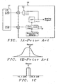
- FIG. 1A is shown a block diagram of prior art for trimming a circuit under trim (CUT) 11 on an integrated circuit chip 10.
- the purpose of trimming is to overcome chip process variations in order to provide a more accurate analog signal and improve chip yield.
- the trimming operation is performed using automatic test equipment (ATE) to deliver digital trim data to the chip and monitor the analog trim values created by a CUT, which results from the digital trim data.
- ATE automatic test equipment
- an ATE 12 connects digital trim data to core logic 13 on the integrated circuit chip 10 where it is stored in a register 14.
- the core logic 13 connects the digital trim data to the CUT 11, which produces an analog signal.
- the analog signal is connected back to the ATE through an analog multiplexer 14.
- the ATE measures the untrimmed value of the analog signal and calculates a digital trim value that is connected to the core logic 13.
- the trim value is connected to the CUT where the process can be iterative depending upon the measured results of the trimmed analog signal output of the CUT. Once a trimmed value has been determined, the trim value is stored in a nonvolatile memory on the integrated circuit chip 10. The trim operation is performed in series with further testing of the integrated circuit and consumes valuable test time.
- FIG. 1B shows how the natural distribution of a trimmed output of the CUT might be not centered where the target trim value is off center in on direction or another depending upon the algorithm used in trimming the CUT.
- FIG. 1C shows an ideal block distribution where the target value is centered within a +1/2 and a - 1/2 least significant bit (LSB).
- CUT circuit under trim
- circuitry contained on an integrated circuit chip is used to both perform a self-test and self trim of a CUT freeing the ATE to perform tests on the integrated circuit chip on functions not related to the CUT and the trimming of the CUT while the self-test and self-trim operations are being carried out.
- the self-trim operation is set up by the ATE and is then carried out by a state machine contained within the integrated circuit chip.
- An LSB offset controlled by the state machine is used to determine the final setting of the CUT. After the trim value is determined, the value is stored in a nonvolatile memory. The successful completion of trim operations of a CUT provides a test for stuck at fault of the associated circuitry.
- FIG.2A is shown a block diagram of the digital self-test and self-trim circuitry of the present invention.
- An ATE 20 is connected to a load board or probe card 21 which is connected to an integrated circuit under test 22.
- the ATE connects an analog reference signal to the integrated circuit chip from a D/A converter circuit 30, and a digital signal connected to core logic 23 through a Dig driver 31.
- the D/A converter 30 in the ATE 20 couples an analog reference signal to a comparator 28 within the integrated circuit 22 under trim and test.
- the core logic comprises a register stack 24 for holding digital data from the ATE and a state machine (SM) 25 for controlling self-test and self-trim operations.
- SM state machine
- a nonvolatile memory 26 is connected to the register stack to store a final trim value to be used to control the analog output of the circuit under trim (CUT) 27 once trimming of the CUT has been completed.
- a comparator circuit 28 comprises an offset input 29 controlled by the state machine 25 that is used in both the self-test and self-trim operations to determine the proper trim value to store in the nonvolatile memory 26.
- the state machine 25 controls switch S1 to position "2", which allows the reference 30 to be connected to both the plus and minus input of the comparator 28. Alternatively both inputs can be connected to the output of the CUT. Then the state machine 25 measures the output of the comparator. Without any offset control, the output of the comparator will be either a logical "0" state or a logical "1" state depending on semiconductor process differences in the input circuitry. The state machine then couples an offset 29 with first a positive and then a negative polarity to cause the output of the comparator 28 to switch to an expected state.
- the output of the comparator changes state from a plus to a minus value or from a minus to a positive value, the operation of the comparator circuit is verified.
- the amount of offset should be high enough to allow some intrinsic offset of the comparator caused by the semiconductor process but small enough to produce a sensible test result, for instance. an offset window equivalent of +/-0.5 LSB of the CUT.
- Another sensible option would be -0.5/+1.0 LSB as a window of 1.5 LSB is beneficial for the self-test of the trim result (as described later).
- analog signal output of the CUT 27 can be either a voltage or a current, wherein the comparator is configured accordingly to compare the analog output of the CUT 27 to a voltage or a current, respectively.
- FIG. 2B Before continuing with self trim operations.
- FIG. 2B is shown an ideal representation of the trimming of the CUT 27 to a reference value where the target value is centered in the block distribution.
- any final digital trim will result in a block distribution 35 that is distributed around a mean digital distribution value (called target) by +0.5 and - 0.5 of the LSB.
- target mean digital distribution value
- This distribution results from variations in the process that produced the various integrated circuit chips located on the same wafer, same batch of wafers and between batches of wafer. The variation can also be produced from minor defects that do not prevent the particular circuitry from operating properly if an adjustment (trim) is performed.
- a self-trim algorithm based on a comparator output will produce a block distribution on one side of the reference; however this block distribution will not be symmetrical around the reference as shown in FIG. 1C . Depending upon the algorithm used, the block distribution will be one side 35 of the reference or the other.
- a linear search algorithm provides the easiest to understand with respect to the behavior of the search results. In a linear search the state machine 25 ( FIG. 2A ) increases the digital trim value until the output of the comparator 28 switches state (trips). When the comparator 28 trips, the search algorithm stops, but the digital trimmed value 35 is now beyond the reference. The search algorithm could decide to choose the digital trim value before the trip point, but the distribution would again be on one side of the reference.
- the result would again be found at one side or the other of the reference.
- the comparator is designed with an intentional default offset of 0.5 LSB (see self-test of comparator) this offset can be used to compensate the single-sided effect as just described.
- the reference has to be chosen 0.5 LSB away from the target.
- a further switchable offset 29 is activated that changes the output of the comparator back to the value before the trip occurred.
- This verification offset 29 needs to be greater than 1.0 LSB in order to allow circuitry that produces a result at the far extreme of the block distribution 35 from the reference.
- a suitable value of the verification offset 29 is 1.5 LSB. As shown in FIG. 2C it is able to prove that the entire distribution will trip the comparator when the verification offset is activated.
- FIG. 2C Shown in FIG. 2C is the effect of an LSB offset 36 where 1.5 LSB is used to guarantee that a trimmed value, which is at the opposite end of the block distribution from the reference, can switch the output state of the comparator circuit.
- a reference that is 0.5 LSB beyond the target can be chosen as exemplified in FIG. 2B when an offset 29 ( FIG. 2A ) of 1.5 LSB is applied to the comparator 28 ( FIG. 2A ).
- Another approach is to superimpose a noise signal of approx. 1 LSB onto the reference connected to the "+" terminal of the comparator 28.
- the state machine then takes several comparator results to decide the trim value, wherein the number of "1" and "0" states of the output of the comparator is used to determine the final result, but this is a complex approach in attempting to overcome a limited resolution of the comparator 28 in the time domain.
- the trim operation of the CUT is set to run autonomously under the control of the state machine 25. It first controls the switch S1 to position "1", which connects the output of the CUT 27 to the comparator 28.
- the digital trim data is stored in the register stack 24 and under the control of the state machine 25 is connected to the CUT 27.
- the switch S1 set in the "1" position to connects the output of the CUT to the minus input of the comparator 28.
- the state machine next controls a search for a digital trim value that allows the CUT to perform to specifications.
- the search can be a linear search as previously discussed, or other algorithms including successive approximation. In all cases the final trim value of the CUT produces a result similar to that discussed with FIG. 2B .
- the search is stopped by the state machine and an offset is introduced to the input of the comparator 29. The intent of the offset is to verify that the last search step was within the allowable tolerance of the trimmed CUT. If the output of the comparator returns to the state previous to the tripping of the comparator, then the digital trim data is stored into the nonvolatile memory to be used to set up the CUT in an operational environment. The choice of which digital trim data is to be stored, before or after the comparator is tripped is dependent upon the choices made for a particular semiconductor product. In either case the final digital trim setting will produce an output from the CUT that is be within the offset of the reference signal.
- FIG. 3A shows a test time line (t) where trimming of circuitry internal to an integrated circuit chip (Trim) is serially performed with tests to the integrated circuit chip (Test), which are not involved with the trim operation .
- the trimming of circuitry such as discussed with the aforementioned CUT takes up valuable test time for the integrated circuit.
- self-trim operations including any self-test operations of the trim circuitry, are performed in parallel with test operations (Test) not involved with the self-trim operations as shown in FIG. 3B , a substantial reduction in total time to test and trim the integrated circuit chip is realized.
- the trim operation is started by the ATE and thereafter runs autonomously in parallel with testing by the ATE of circuitry not associated with the circuitry being trimmed. As can be observed from FIG.
- the TRIM operation starts delayed from the start of the TEST operation performed by the ATE. This is to allow the ATE to set up the trim operation including connecting trim data to the circuitry performing the trim operation.
- the ATE collects the trim results and logs the data resulting from the trim operation.
- FIG. 4 is shown a block diagram of the present invention for trimming a CUT contained on an integrated circuit chip 40 comprising an oscillator that runs a clock on an integrated circuit chip 40.
- a CUT 41 comprising an oscillator, which may be formed by a VCO (voltage controlled oscillator) or other means that can be controlled from digital data, is frequency trimmed by the connection of digital data from a register stack 42 under the control of a state machine 43.
- the output of the CUT 41 is connected to a first n-bit counter 45.
- An external reference clock 46 which may exist in a tester, is connected to a second n-bit counter 47.
- the output of the first n-bit counter 45 is connected to a first flip-flop circuit 48 that is clocked by the second n-bit counter 47.
- the first flip-flop 48 is connected to a second flip-flop 49 that is clocked by the reference clock 46.
- a result formed by the output of the second flip-flop 49 is connected to the state machine 43.
- Digital data 50 that contains trim data for trimming the frequency of the oscillator CUT 41 is connected from an ATE to the register stack 42 contained within core logic and the state machine of the integrated circuit chip 40.
- both the first and second n-bit counters 45, 47 are reset, which in turn opens the first flip flop 48 to receive a signal from the first counter 45.
- the first flip flop circuit is clocked off by the second n-bit counter, and a "Ready" signal is produced indicating that the result of the trim step can be evaluated before the state machine proceeds by connecting a new trim value to the CUT 41. If the frequency of the CUT 41 is less than the frequency of the reference clock 46, the result captured in the flip-flop 48 will be a logical "0".
- the result captured in the flip-flop 48 will be a logical "1".
- the result value is coupled to the state machine 43 through a second flip-flop 49 in order to let possible metastability of flip-flop 48 settle.
- the CUT oscillator 41 is verified to be trimmed to within the offset 51.
- the offset difference is 1.5 LSB (-0.5 to 1.0 LSB) as previously discussed with respect to FIG. 2A and 2B , and the final and verified trim value of the CUT is stored into the nonvolatile memory 52.
- Both the first and the second n-bit counters are reset at the same time with the reset of second n-bit counter 47 comprising an offset 51 that is equivalent to - 0.5 LSB trimming step size.
- the state machine 43 connects different digital values stored in the register 42 to the CUT oscillator 41. After the trim algorithm has finished the offset is switched to +1.0 LSB and the trim setting of the CUT that produced the change of state is compared to the reference clock without the offset being imposed.
- trim circuit is used to adjust time t, for example a pulse width of a time related signal.
- the first one is a binary search trim of the oscillator CUT 41 shown in FIG. 4 .
- the second one is a linear search algorithm.
- the binary search tends to be faster and adapts well to the binary coding of the trim value.
- the self-test of the comparator is omitted as the comparator is implemented with digital logic that is assumed to be tested according to digital scan test principles.
- the 1.5 LSB verification step is at the end of each algorithm and is done once, not after every modification of the trim value. It should also be noted that similar algorithms can be written to trim the CUT 27 shown in FIG. 2A .
- the second exemplary algorithm is a linear search of a comparator threshold. Again the comparator self-test can be omitted as the offset itself is the value to be trimmed.
- the linear search algorithm is applied, wherein the comparator has a built-in hysteresis.
Landscapes
- Engineering & Computer Science (AREA)
- General Engineering & Computer Science (AREA)
- Physics & Mathematics (AREA)
- General Physics & Mathematics (AREA)
- Semiconductor Integrated Circuits (AREA)
- Tests Of Electronic Circuits (AREA)
Description
- The present invention is related to calibration and testing of semiconductor chips and in particular to the self-trimming and self-testing of on-chip analog values.
- Integrated circuits use a wide collection of analog circuitry to enable the function of the integrated circuits ranging from reference voltages to reference currents, offsets, comparator thresholds and oscillator frequencies. Imperfection in the manufacture of the chips containing the integrated circuits results in the need to trim the values produced by the analog circuitry to produce a chip that might not function properly as designed. When performing multi-site testing, for instance semiconductor chips on a wafer, trimming cannot be done in parallel because the ATE (automatic test equipment) must react to the individual behavior of circuits on the various chips, individually calculate trim values and then send these values to the individual circuits.
- In
US Patent Application Publication No. 2006/02474594 A1 (Huckaby et al. US Patent Application Publication No. 2007/0133319 A1 (Noichi ) is directed to a current generator wherein the current output is adjusted with trimming data stored in a nonvolatile memory cell. InUS Patent Application Publication No. 2008/0012596 A1 (Lewison et al. ) trim codes are directed to semiconductor devices under test (DUT), which cause the DUT to generate voltage or current reference values.US Patent Application Publication No. 2001/0004126 A1 (Ohlhoff ) is directed to a circuit for trimming reference voltages in semiconductor chips, wherein test logic and a trimming circuit are used to trim reference voltages.US Patent Application Publication No. 2006/02769886 A1 (Anderson et al. Japanese Patent Publication Number 2004179505 (Kobayashi Masanori -
US 7,352,230 B2 (An ) is directed to an internal power voltage trimming circuit and a method for individually or simultaneously performing level trimming for a plurality of power voltages in a semiconductor memory device.US 7,284,167 (Le et al. ) is directed to a method for providing programmable test conditions used in a BIST for a flash memory device. InUS 6,943,616 B2 (Ogawa et al. ) an integrated circuit device and method is directed to adjusting an analog signal output without outputting the analog signal outside the integrated circuit device.US 6,909,642 B2 (Lehmann et al. ) is directed to integrated circuit chips having self-adjusting internal voltages and the method thereof. InUS 6,504,394 B2 (Ohlhoff ) a circuit is directed to a configuration for trimming reference voltages within integrated circuit chips.US 6,433,714 (Clapp et al.) is directed to methods and apparatus for trimming semiconductor devices and circuits. InUS 6,114,920 (Moon et al. ) an auto-trim is directed to trimming a PLL oscillator operating curve for use during normal operations, wherein a state machine applies a digital control to a VCO during the auto-trim that is to be used in normal operations. -
US 6,111,471 (Bonneau et al. ) is directed to an apparatus for setting the free-running frequency of a VCO to a reference frequency and comprises setting the VCO within a frequency range and between frequency ranges. InUS 5,550,512 (Fukahori ) a method is directed to providing a DC offset trim for automatic gain control independent of temperature and gain using a trim current connected to an AGC circuit.US 5,319,370 (Signore et al. ) is directed to a method and apparatus for calibrating errors in an analog reference voltage input to an ADC using a delta-sigma A/D converter. - In
FIG. 1A is shown a block diagram of prior art for trimming a circuit under trim (CUT) 11 on anintegrated circuit chip 10. The purpose of trimming is to overcome chip process variations in order to provide a more accurate analog signal and improve chip yield. The trimming operation is performed using automatic test equipment (ATE) to deliver digital trim data to the chip and monitor the analog trim values created by a CUT, which results from the digital trim data. As shown inFIG. 1A , an ATE 12 connects digital trim data tocore logic 13 on theintegrated circuit chip 10 where it is stored in aregister 14. Thecore logic 13 connects the digital trim data to theCUT 11, which produces an analog signal. The analog signal is connected back to the ATE through ananalog multiplexer 14. The ATE measures the untrimmed value of the analog signal and calculates a digital trim value that is connected to thecore logic 13. The trim value is connected to the CUT where the process can be iterative depending upon the measured results of the trimmed analog signal output of the CUT. Once a trimmed value has been determined, the trim value is stored in a nonvolatile memory on theintegrated circuit chip 10. The trim operation is performed in series with further testing of the integrated circuit and consumes valuable test time. -
FIG. 1B shows how the natural distribution of a trimmed output of the CUT might be not centered where the target trim value is off center in on direction or another depending upon the algorithm used in trimming the CUT.FIG. 1C shows an ideal block distribution where the target value is centered within a +1/2 and a - 1/2 least significant bit (LSB). - It is an objective of the present invention to provide a self-trim capability, which produces a trimmed circuit under trim (CUT) where the trimming process is independent of the ATE and allows testing not related to the CUT to proceed in parallel with the trimming process.
- It is also an objective of the present invention to provide self-test of the a comparator circuit used in measuring the trim value as well as stuck-at faults in the digital signals connected to the CUT.
- It is further an objective of the present invention to use an LSB offset to produce a trim value that is within an LSB of an analog reference.
- It is still further an objective of the present invention to use the capability to provide an LSB offset to self-test a comparator circuit used to detect when a CUT has been trimmed.
- In the present invention circuitry contained on an integrated circuit chip is used to both perform a self-test and self trim of a CUT freeing the ATE to perform tests on the integrated circuit chip on functions not related to the CUT and the trimming of the CUT while the self-test and self-trim operations are being carried out. The self-trim operation is set up by the ATE and is then carried out by a state machine contained within the integrated circuit chip. An LSB offset controlled by the state machine is used to determine the final setting of the CUT. After the trim value is determined, the value is stored in a nonvolatile memory. The successful completion of trim operations of a CUT provides a test for stuck at fault of the associated circuitry.
- This invention will be described with reference to the accompanying drawings, wherein:
-
FIG. 1A shows a block diagram of prior art for trimming a CUT under the control of an ATE; -
FIG. 1B shows a natural distribution of trim values obtained by prior art trimming operations; -
FIG. 1C show an ideal block distribution of trim values center about plus and minus ½ LSB; -
FIG. 2A is a block diagram of a digital self-trim configuration of the present invention; -
FIG. 2B is a distribution of a self-trim operation by the present invention; -
FIG. 2C is a distribution of a self-test operation of the present invention; -
FIG. 3A is a test time line of prior art where trim operations test operations are controlled to be serial; -
FIG. 3B is a test time line for the present invention where trim operations are performed in parallel with a portion of test on an integrated circuit chip; and -
FIG. 4 is a block diagram of the present invention of a self-trim of an oscillator clock frequency. - In
FIG.2A is shown a block diagram of the digital self-test and self-trim circuitry of the present invention. An ATE 20 is connected to a load board orprobe card 21 which is connected to an integrated circuit undertest 22. The ATE connects an analog reference signal to the integrated circuit chip from a D/A converter circuit 30, and a digital signal connected tocore logic 23 through aDig driver 31. The D/A converter 30 in the ATE 20 couples an analog reference signal to acomparator 28 within the integratedcircuit 22 under trim and test. The core logic comprises aregister stack 24 for holding digital data from the ATE and a state machine (SM) 25 for controlling self-test and self-trim operations. Anonvolatile memory 26 is connected to the register stack to store a final trim value to be used to control the analog output of the circuit under trim (CUT) 27 once trimming of the CUT has been completed. Acomparator circuit 28 comprises an offsetinput 29 controlled by thestate machine 25 that is used in both the self-test and self-trim operations to determine the proper trim value to store in thenonvolatile memory 26. - To self-test the
comparator 28, thestate machine 25 controls switch S1 to position "2", which allows thereference 30 to be connected to both the plus and minus input of thecomparator 28. Alternatively both inputs can be connected to the output of the CUT. Then thestate machine 25 measures the output of the comparator. Without any offset control, the output of the comparator will be either a logical "0" state or a logical "1" state depending on semiconductor process differences in the input circuitry. The state machine then couples an offset 29 with first a positive and then a negative polarity to cause the output of thecomparator 28 to switch to an expected state. If the output of the comparator changes state from a plus to a minus value or from a minus to a positive value, the operation of the comparator circuit is verified. The amount of offset should be high enough to allow some intrinsic offset of the comparator caused by the semiconductor process but small enough to produce a sensible test result, for instance. an offset window equivalent of +/-0.5 LSB of the CUT. Another sensible option would be -0.5/+1.0 LSB as a window of 1.5 LSB is beneficial for the self-test of the trim result (as described later). - It should be noted that it is within the scope of this invention that the analog signal output of the
CUT 27 can be either a voltage or a current, wherein the comparator is configured accordingly to compare the analog output of theCUT 27 to a voltage or a current, respectively. - Consider
FIG. 2B before continuing with self trim operations. InFIG. 2B is shown an ideal representation of the trimming of theCUT 27 to a reference value where the target value is centered in the block distribution. Because of limited digital resolution, any final digital trim will result in ablock distribution 35 that is distributed around a mean digital distribution value (called target) by +0.5 and - 0.5 of the LSB. This distribution results from variations in the process that produced the various integrated circuit chips located on the same wafer, same batch of wafers and between batches of wafer. The variation can also be produced from minor defects that do not prevent the particular circuitry from operating properly if an adjustment (trim) is performed. - A self-trim algorithm based on a comparator output will produce a block distribution on one side of the reference; however this block distribution will not be symmetrical around the reference as shown in
FIG. 1C . Depending upon the algorithm used, the block distribution will be oneside 35 of the reference or the other. A linear search algorithm provides the easiest to understand with respect to the behavior of the search results. In a linear search the state machine 25 (FIG. 2A ) increases the digital trim value until the output of thecomparator 28 switches state (trips). When thecomparator 28 trips, the search algorithm stops, but the digital trimmedvalue 35 is now beyond the reference. The search algorithm could decide to choose the digital trim value before the trip point, but the distribution would again be on one side of the reference. If the search were done from the other side of the trim range, the result would again be found at one side or the other of the reference. Thus the only choice is to choose which side of the reference is preferred. If the comparator is designed with an intentional default offset of 0.5 LSB (see self-test of comparator) this offset can be used to compensate the single-sided effect as just described. Alternatively the reference has to be chosen 0.5 LSB away from the target. - In order to verify if the analog trim value that tripped the
comparator 28 is within the expected distance of 1.0 LSB from the reference, a further switchable offset 29 is activated that changes the output of the comparator back to the value before the trip occurred. This verification offset 29 needs to be greater than 1.0 LSB in order to allow circuitry that produces a result at the far extreme of theblock distribution 35 from the reference. A suitable value of the verification offset 29 is 1.5 LSB. As shown inFIG. 2C it is able to prove that the entire distribution will trip the comparator when the verification offset is activated. - Shown in
FIG. 2C is the effect of an LSB offset 36 where 1.5 LSB is used to guarantee that a trimmed value, which is at the opposite end of the block distribution from the reference, can switch the output state of the comparator circuit. Thus a reference that is 0.5 LSB beyond the target can be chosen as exemplified inFIG. 2B when an offset 29 (FIG. 2A ) of 1.5 LSB is applied to the comparator 28 (FIG. 2A ). Another approach is to superimpose a noise signal of approx. 1 LSB onto the reference connected to the "+" terminal of thecomparator 28. The state machine then takes several comparator results to decide the trim value, wherein the number of "1" and "0" states of the output of the comparator is used to determine the final result, but this is a complex approach in attempting to overcome a limited resolution of thecomparator 28 in the time domain. - Returning to
FIG. 2A , once theDig 31 has connected digital trim data to thecore logic 23 and the analog reference signal has been connected from the D/A 30 to the positive input of thecomparator 28, the trim operation of the CUT is set to run autonomously under the control of thestate machine 25. It first controls the switch S1 to position "1", which connects the output of theCUT 27 to thecomparator 28. The digital trim data is stored in theregister stack 24 and under the control of thestate machine 25 is connected to theCUT 27. The switch S1 set in the "1" position to connects the output of the CUT to the minus input of thecomparator 28. - The state machine next controls a search for a digital trim value that allows the CUT to perform to specifications. The search can be a linear search as previously discussed, or other algorithms including successive approximation. In all cases the final trim value of the CUT produces a result similar to that discussed with
FIG. 2B . After the algorithm has finished, the search is stopped by the state machine and an offset is introduced to the input of thecomparator 29. The intent of the offset is to verify that the last search step was within the allowable tolerance of the trimmed CUT. If the output of the comparator returns to the state previous to the tripping of the comparator, then the digital trim data is stored into the nonvolatile memory to be used to set up the CUT in an operational environment. The choice of which digital trim data is to be stored, before or after the comparator is tripped is dependent upon the choices made for a particular semiconductor product. In either case the final digital trim setting will produce an output from the CUT that is be within the offset of the reference signal. -
FIG. 3A shows a test time line (t) where trimming of circuitry internal to an integrated circuit chip (Trim) is serially performed with tests to the integrated circuit chip (Test), which are not involved with the trim operation . The trimming of circuitry such as discussed with the aforementioned CUT takes up valuable test time for the integrated circuit. If self-trim operations (Trim), including any self-test operations of the trim circuitry, are performed in parallel with test operations (Test) not involved with the self-trim operations as shown inFIG. 3B , a substantial reduction in total time to test and trim the integrated circuit chip is realized. The trim operation is started by the ATE and thereafter runs autonomously in parallel with testing by the ATE of circuitry not associated with the circuitry being trimmed. As can be observed fromFIG. 3B the TRIM operation starts delayed from the start of the TEST operation performed by the ATE. This is to allow the ATE to set up the trim operation including connecting trim data to the circuitry performing the trim operation. When the trim operation is completed the ATE collects the trim results and logs the data resulting from the trim operation. - In
FIG. 4 is shown a block diagram of the present invention for trimming a CUT contained on anintegrated circuit chip 40 comprising an oscillator that runs a clock on anintegrated circuit chip 40. ACUT 41 comprising an oscillator, which may be formed by a VCO (voltage controlled oscillator) or other means that can be controlled from digital data, is frequency trimmed by the connection of digital data from aregister stack 42 under the control of astate machine 43. The output of theCUT 41 is connected to a first n-bit counter 45. Anexternal reference clock 46, which may exist in a tester, is connected to a second n-bit counter 47. The output of the first n-bit counter 45 is connected to a first flip-flop circuit 48 that is clocked by the second n-bit counter 47. - The first flip-
flop 48 is connected to a second flip-flop 49 that is clocked by thereference clock 46. A result formed by the output of the second flip-flop 49 is connected to thestate machine 43. The state of the resulting output of the second flip-flop 49 depends on the frequency of the CUT oscillator compared to thereference oscillator 46 such that the result=0 if the CUT oscillator frequency is less than the reference frequency, and the result=1 if the cut oscillator frequency is greater than the reference frequency.Digital data 50 that contains trim data for trimming the frequency of theoscillator CUT 41 is connected from an ATE to theregister stack 42 contained within core logic and the state machine of theintegrated circuit chip 40. - At the beginning of a trim operation and each trim step thereafter, both the first and second n-bit counters 45, 47 are reset, which in turn opens the
first flip flop 48 to receive a signal from thefirst counter 45. When the reference clock signal has expired at the end of the second n-bit counter 47, the first flip flop circuit is clocked off by the second n-bit counter, and a "Ready" signal is produced indicating that the result of the trim step can be evaluated before the state machine proceeds by connecting a new trim value to theCUT 41. If the frequency of theCUT 41 is less than the frequency of thereference clock 46, the result captured in the flip-flop 48 will be a logical "0". If the frequency of theCUT 41 is higher than the frequency of thereference clock 46, the result captured in the flip-flop 48 will be a logical "1". The result value is coupled to thestate machine 43 through a second flip-flop 49 in order to let possible metastability of flip-flop 48 settle. Once the trim algorithm is finished the offset 51 is turned on and the first and second n-bit counters are reset allowing theCUT 41 signal that produced the final trim result (assume "1") to propagate through the first n-bit counter 45 and the reference clock signal to propagate through the second n-bit counter 47, wherein the reset of the second n-bit counter 47 is modified by the amount of the offset 51. Then if the result=0 captured in the flip-flop 48 when the reference clock reaches the end of the second n-bit counter 47 (reset with the offset), theCUT oscillator 41 is verified to be trimmed to within the offset 51. The offset difference is 1.5 LSB (-0.5 to 1.0 LSB) as previously discussed with respect toFIG. 2A and 2B , and the final and verified trim value of the CUT is stored into thenonvolatile memory 52. - Both the first and the second n-bit counters are reset at the same time with the reset of second n-
bit counter 47 comprising an offset 51 that is equivalent to - 0.5 LSB trimming step size. Thestate machine 43 connects different digital values stored in theregister 42 to theCUT oscillator 41. After the trim algorithm has finished the offset is switched to +1.0 LSB and the trim setting of the CUT that produced the change of state is compared to the reference clock without the offset being imposed. If the comparison of the trimmed CUT and the reference clock without the offset produces a change of state of the compare value back to a logical "1", then the trimming of theCUT 41 is confirmed and the digital trim value connected to the CUT oscillator causing the change of state in the results of the first flip-flop is stored in the nonvolatile memory as the oscillator frequency trim value. - It should be noted that although the discussion with respect to
FIG. 4 is oriented towards theCUT 41 being an oscillator, it is within the scope of this invention that the trim circuit is used to adjust time t, for example a pulse width of a time related signal. - The following are exemplary algorithms in Verilog/C-like pseudo code that search for a trim value. The first one is a binary search trim of the
oscillator CUT 41 shown inFIG. 4 . The second one is a linear search algorithm. The binary search tends to be faster and adapts well to the binary coding of the trim value. It should be noted that the self-test of the comparator is omitted as the comparator is implemented with digital logic that is assumed to be tested according to digital scan test principles. The 1.5 LSB verification step is at the end of each algorithm and is done once, not after every modification of the trim value. It should also be noted that similar algorithms can be written to trim theCUT 27 shown inFIG. 2A . - An exemplary bitwise approximation is demonstrated starting with the most significant bit to set the trim bit.
 osc_BIST = TRUE;      // triggered by register write access
 osc_offset = 0x00;
 osc_ok = TRUE;
 osc_trim[4:0] = 0b10000;
 for (i = 4 downto 0)      // successive approximation loop
 {
       osc_trim[i] = 1;
       Wait 8 clock cycles;      // let trim settings settle
       Start comparator;
       while (!ready);      // wait until comparator done
       if (osc_f > ref_f) osc_trim[i] = 0;
       }
       Wait 8 clock cycles;      // let trim settings settle
 osc_offset = 0x08;      //1.5 LSB
 Start comparator; while (!ready);      // verification measurement
 if (osc_f f < ref_f) osc_ok = FALSE;
 osc_BIST = FALSE;      // ready signal to ATE.
 vset_BIST = TRUE;      / triggered by register write access
 vset_Isb_offset = 0;      // -0.5 LSB
 vset_ok = TRUE;
 vset_trim[2:0] = 0b000;
 Wait 8 clock cycles;      // let trim settings settle
 while (!comp_out && vset_trim < 0b111) // linear search
 {
        vset_trim++;      // increment
        Wait 8 clock cycles;
 }
  if (!comp_out) vset_ok = FALSE;      // fail
 vse_lsb_offset = 1;      // +1.0 LSB
  if (comp_out) vset_ok = FALSE;      // verification failed
 vset_BIST = FALSE;      // ready signal to ATE.
Claims (20)
- A self-trim circuit, comprising:a) a circuit under trim,CUT, (27) producing an analog signal and trimmed by a digital self-trim circuit;b) a compare circuit (28) to compare an output of the CUT to a reference signal; andc) a non-volatile memory (26), characterised in that said digital self-trim circuit stores digital trim data that is necessary to trim the CUT (27) to produce said output comparable to the reference signal (30), wherein said digital self-trim circuit searches digital trim bits connected to said CUT (27) to produce said output that changes a state of the compare circuit from a first state to a second state, whereupon an offset (29) connected to the compare circuit (28) determines whether the state of the compare circuit (28) can be changed back to the first state to confirm the output of the CUT (27) to be within a least significant bit, LSB, of the reference signal (30).
- The circuit of claim 1, wherein the LSB has a block distribution of one LSB to account for semiconductor process variations and effects of minor defects.
- The circuit of claim 1, wherein the offset is 1.5 least significant bits.
- The circuit of claim 1, wherein the output of the CUT (27) is a voltage or a current.
- The circuit of claim 1, wherein the output of the CUT (41) is time, further comprising;a) frequency, the reciprocal of time; andb) pulse width.
- The circuit of claim 5, wherein the CUT (41) is an oscillator in which frequency trimming of the CUT (41) further comprises:a) a comparison of outputs of two n-bit counters (45, 47) determines a frequency trim of said CUT (41) relative to a reference clock wherein a first (45) of the two n-bit counters counts the frequency trim of the CUT and a second (47) of the two n-bit counters counts the reference frequency of a reference clock (46), wherein the two n-bit counters are reset at the same time to start the two n-bit counters, whereby an output of the first (45) of the two n-bit counters compared to an output of the second (47) of the two n-bit counters; andb) an offset (51) implemented in the reset of the second (47) of the two n-bit counters after the frequency trim of the CUT (41) reaches the end of the first counter (45) before the reference frequency reaches the end of the second counter (47) to verify the frequency trim within the offset (51).
- The circuit of claim 1, wherein said CUT (27, 41) and said digital circuit is located on an integrated circuit chip (22), wherein said reference signal (30) and said digital data (31) is sourced from automatic test equipment (20) and said trim of the CUT is performed in parallel with other tests performed on the integrated circuit chip by the test equipment.
- The circuit of claim 1, wherein said digital self-trim circuit further comprises a self-test capability using said trim circuitry, further comprising:a) a test of said compare circuit (28), wherein both inputs of said compare circuit are connected to the reference signal or the CUT signal; andb) a switchable offset of a known value connected to the compare circuit by the digital self-trim circuit and wherein the digital self-trim circuit reads the expected response of the compare circuit for both a positive and a negative value offset.
- The self trim circuit of claim 1, wherein an oscillator circuit is the circuit under trim, CUT (41), which further comprises:a) a frequency generating circuit, wherein an output is capable of producing a digital signal when the output of the frequency generating circuit reaches a predetermined number of cycles;b) a first digital circuit comprising a first n-bit counter (45) to count the output of oscillator circuit under trim (41), CUT, capable of producing a first digital signal, and a second digital circuit comprising a second n-bit counter (47) to count an output of a reference clock (46) capable of producing a second digital signal, wherein the first digital signal is compared to the second digital signal in a flip-flop circuit (48);c) said oscillator circuit under trim (41), CUT, capable of being digitally adjusted forming a digital trim value;d) said second digital circuit (47) capable of providing a start condition offset 51 for verifying output frequency of the CUT (41) trimmed within said offset; ande) the nonvolatile memory (52) capable of storing the digital trim value
- The self trim circuit of claim 9, wherein said CUT (41) capable of producing the first digital signal that Is counted by a first n-bit counter (45), and the reference clock (46) capable of producing the second digital signal that is counted by a second n-bit counter (47).
- The self trim circuit of claim 10, wherein said first digital circuit (45), capable of producing the first digital signal, is applied to a flip-flop circuit (48), and the second digital circuit (47), capable of producing the second digital signal, clocks the flip-flopcircuit (48) to determine whether the frequency of the first digital signal is faster, or slower, than the second digital signal produced by the reference clock..
- The self trim circuit of claim 9, wherein said CUT (41) capable of producing an oscillating frequency is controlled by core logic located on the same semiconductor chip as the CUT (41), wherein the core logic comprises a state machine (43), and a register stack (42), and communicates with the CUT (41) with digital circuitry.
- The self trim circuit of claim 9, wherein said second digital circuit (47) capable of producing start condition for the second digital signal that is offset (51) to produce a delay in the reset of the second n-bit counter (47), which is greater than an equivalent of the least significant bit, LSB, of the digital trim value.
- A method of self-test and self-trim, comprising:a) self-trimming a circuit under trim, CUT (27), contained within said integrated circuit device (22);b) loading a register stack (24)with a plurality of digital trim values to trim the CUT (27) to produce a specified output;c) coupling an output of the CUT (27) to a first input of a comparator circuit (28) and the reference signal to a second input of the comparator circuit (28);c) applying said digital trim values to the CUT (27), one after another, until output of said comparator circuit (28) changes state; thene) applying a verification offset to the comparator circuit (28) to force output of said comparator circuit to change back to the prior state and thereby verifying the self-trimming of the CUT (27) is within the verification offset of a least significant bit; andf) storing into a nonvolatile memory (26) the digital trim value causing the state change in comparator circuit output.
- The method of claim 14, wherein the verification offset is 1.5 least significant bits.
- The method of claim 14, wherein the output of the CUT (27) is voltage or a current.
- The method of claim 14, wherein the output of the CUT is time, further comprising;a) frequency; andb) pulse width.
- The method of claim 14, wherein said register stack is loaded from automatic test equipment (20).
- The method of claim 14, wherein said self-trimming of the CUT is controlled by a state machine (25).
- The method of claim 14, wherein the comparator circuit is self-tested, comprising the following steps:a) connecting a reference signal to both input of the comparator circuit (28);b) applying first a positive, then a negative offset to the comparator circuit; andc) reading an output of the comparator circuit (28) with a state machine (25) to detect change of state of the comparator circuit (28).
Priority Applications (2)
| Application Number | Priority Date | Filing Date | Title |
|---|---|---|---|
| EP09392001.5A EP2253966B1 (en) | 2009-05-18 | 2009-05-18 | Self-trim and self-test of on-chip values |
| US12/455,530 US8143953B2 (en) | 2009-05-18 | 2009-06-03 | Self-trim and self-test of on-chip values |
Applications Claiming Priority (1)
| Application Number | Priority Date | Filing Date | Title |
|---|---|---|---|
| EP09392001.5A EP2253966B1 (en) | 2009-05-18 | 2009-05-18 | Self-trim and self-test of on-chip values |
Publications (2)
| Publication Number | Publication Date |
|---|---|
| EP2253966A1 EP2253966A1 (en) | 2010-11-24 |
| EP2253966B1 true EP2253966B1 (en) | 2014-04-30 |
Family
ID=41128587
Family Applications (1)
| Application Number | Title | Priority Date | Filing Date |
|---|---|---|---|
| EP09392001.5A Not-in-force EP2253966B1 (en) | 2009-05-18 | 2009-05-18 | Self-trim and self-test of on-chip values |
Country Status (2)
| Country | Link |
|---|---|
| US (1) | US8143953B2 (en) |
| EP (1) | EP2253966B1 (en) |
Families Citing this family (13)
| Publication number | Priority date | Publication date | Assignee | Title |
|---|---|---|---|---|
| JP2011033488A (en) * | 2009-08-03 | 2011-02-17 | Renesas Electronics Corp | Semiconductor integrated circuit test device |
| EP2487797B1 (en) | 2011-02-11 | 2014-04-09 | Dialog Semiconductor GmbH | Minimum differential non-linearity trim DAC |
| US8363477B2 (en) * | 2011-03-09 | 2013-01-29 | Ememory Technology Inc. | Method of setting trim codes for a flash memory and related device |
| WO2013134444A1 (en) * | 2012-03-06 | 2013-09-12 | Waveconnex, Inc. | System for constraining an operating parameter of an ehf communication chip |
| US9038133B2 (en) | 2012-12-07 | 2015-05-19 | International Business Machines Corporation | Self-authenticating of chip based on intrinsic features |
| CN104242925B (en) | 2013-06-18 | 2017-05-17 | 中芯国际集成电路制造(上海)有限公司 | Frequency generating device, method and equipment |
| US9356590B1 (en) | 2014-12-16 | 2016-05-31 | Freescale Semiconductor, Inc. | Production test trimming acceleration |
| CN108023589B (en) * | 2016-11-03 | 2021-06-22 | 深圳市中兴微电子技术有限公司 | Frequency calibration method and circuit |
| US11056210B1 (en) | 2020-02-13 | 2021-07-06 | Dialog Semiconductor (Uk) Limited | Electrical circuit comprising a trim circuit |
| CN113805033B (en) * | 2020-06-12 | 2024-02-06 | 圣邦微电子(北京)股份有限公司 | Trimming method for chip voltage |
| CN114002588B (en) * | 2022-01-04 | 2022-04-29 | 苏州贝克微电子股份有限公司 | High-precision semiconductor chip trimming test method |
| EP4453940A1 (en) * | 2022-01-27 | 2024-10-30 | Siemens Industry Software Inc. | Memory built-in self-test with address skipping trim search |
| EP4564665A1 (en) | 2023-11-30 | 2025-06-04 | Nxp B.V. | Built-in self-test system and method for crystal oscillator amplifier |
Family Cites Families (20)
| Publication number | Priority date | Publication date | Assignee | Title |
|---|---|---|---|---|
| IL96351A (en) * | 1990-11-14 | 1994-01-25 | Zuta Marc | Frequency synthesizer having microcomputer supplying analog and digital control signals to vco |
| US5319370A (en) | 1992-08-31 | 1994-06-07 | Crystal Semiconductor, Inc. | Analog-to-digital converter with a continuously calibrated voltage reference |
| US5432475A (en) | 1994-06-15 | 1995-07-11 | Silicon Systems, Inc. | Method of offset voltage trim for automatic gain controls |
| IL120119A0 (en) * | 1997-01-31 | 1997-04-15 | Binder Yehuda | Method and system for calibrating a crystal oscillator |
| US5942949A (en) | 1997-10-14 | 1999-08-24 | Lucent Technologies Inc. | Self-calibrating phase-lock loop with auto-trim operations for selecting an appropriate oscillator operating curve |
| US6111471A (en) | 1998-05-28 | 2000-08-29 | International Business Machines Corporation | Apparatus and method for setting VCO free-running frequency |
| US6124764A (en) * | 1999-01-22 | 2000-09-26 | Telefonaktiebolaget Lm Ericsson | Stable low-power oscillator |
| DE19960244C1 (en) * | 1999-12-14 | 2001-02-01 | Infineon Technologies Ag | Arrangement for trimming reference voltages in semiconducting chips enables rapid and cost-effective reference voltage trimming |
| US6433714B1 (en) | 2000-12-20 | 2002-08-13 | Agere Systems Guardian Corp. | Apparatus and method for precision trimming of a semiconductor device |
| JP2004146783A (en) | 2002-08-28 | 2004-05-20 | Fujitsu Ltd | Semiconductor integrated circuit device and method of adjusting semiconductor integrated circuit device |
| JP2004179505A (en) * | 2002-11-28 | 2004-06-24 | Seiko Epson Corp | Semiconductor integrated circuit and method of manufacturing the same |
| US6909642B2 (en) | 2003-03-14 | 2005-06-21 | Infineon Technologies North American Corp. | Self trimming voltage generator |
| KR100605596B1 (en) | 2004-09-22 | 2006-07-28 | 주식회사 하이닉스반도체 | Internal Power Supply Voltage Trimming Circuit and Method for Semiconductor Memory Devices |
| US7284167B2 (en) | 2005-01-24 | 2007-10-16 | Spansion Llc | Automated tests for built-in self test |
| US7277350B2 (en) * | 2005-06-01 | 2007-10-02 | Infineon Technologies Ag | Implementation of a fusing scheme to allow internal voltage trimming |
| US7433790B2 (en) * | 2005-06-06 | 2008-10-07 | Standard Microsystems Corporation | Automatic reference voltage trimming technique |
| US7890787B2 (en) * | 2005-06-17 | 2011-02-15 | Analog Devices, Inc. | Microprocessor programmable clock calibration system and method |
| JP4942990B2 (en) * | 2005-12-12 | 2012-05-30 | パナソニック株式会社 | Semiconductor memory device |
| US7423445B2 (en) * | 2006-07-17 | 2008-09-09 | Qimonda North America Corp. | Method and system for trimming voltage or current references |
| US7855610B2 (en) * | 2008-05-07 | 2010-12-21 | Qualcomm Incorporated | VCO capacitor bank trimming and calibration |
-
2009
- 2009-05-18 EP EP09392001.5A patent/EP2253966B1/en not_active Not-in-force
- 2009-06-03 US US12/455,530 patent/US8143953B2/en active Active
Also Published As
| Publication number | Publication date |
|---|---|
| US20100289590A1 (en) | 2010-11-18 |
| US8143953B2 (en) | 2012-03-27 |
| EP2253966A1 (en) | 2010-11-24 |
Similar Documents
| Publication | Publication Date | Title |
|---|---|---|
| US8143953B2 (en) | Self-trim and self-test of on-chip values | |
| US7271751B2 (en) | Digital BIST test scheme for ADC/DAC circuits | |
| JP3453133B2 (en) | Timing calibration method for IC test apparatus and IC test apparatus having calibration function using the calibration method | |
| US7474974B2 (en) | Embedded time domain analyzer for high speed circuits | |
| US6829737B1 (en) | Method and system for storing device test information on a semiconductor device using on-device logic for determination of test results | |
| US9134374B2 (en) | Circuit and method for measuring delays between edges of signals of a circuit | |
| US20070124092A1 (en) | Internal bias measure with onboard ADC for electronic devices | |
| US20080008012A1 (en) | Implementation of a fusing scheme to allow internal voltage trimming | |
| US8058893B1 (en) | Frequency trimming for internal oscillator for test-time reduction | |
| WO2011068904A2 (en) | REAL-TIME ADAPTIVE HYBRID BiST SOLUTION FOR LOW-COST AND LOW-RESOURCE ATE PRODUCTION TESTING OF ANALOG-TO-DIGITAL CONVERTERS | |
| CN114815943B (en) | Correction and trimming circuit and integrated circuit | |
| US6057691A (en) | Delay element testing apparatus and integrated circuit having testing function for delay elements | |
| US20160349318A1 (en) | Dynamic Clock Chain Bypass | |
| US20200336151A1 (en) | Real time counter-based method for the determination and measurement of frequency lock time in phase-locked loops | |
| US20090216388A1 (en) | Wafer and temperature testing method of the same | |
| US7804371B2 (en) | Systems, modules, chips, circuits and methods with delay trim value updates on power-up | |
| US9702929B2 (en) | Test apparatus | |
| US9003244B2 (en) | Dynamic built-in self-test system | |
| US8583973B1 (en) | Stored-pattern logic self-testing with serial communication | |
| US6470483B1 (en) | Method and apparatus for measuring internal clock skew | |
| US20140365838A1 (en) | Integrated circuit comprising test circuitry for testing fan-out paths of a test control primary input | |
| US6873557B2 (en) | Integrated circuit device with a built-in detecting circuit for detecting maximum memory access time of an embedded memory | |
| CN113504457B (en) | Circuit testing device and method for improving detection precision | |
| US12332303B2 (en) | Built-in self test with current measurement for analog circuit verification | |
| TW202147112A (en) | Method and system for testing an integrated circuit |
Legal Events
| Date | Code | Title | Description |
|---|---|---|---|
| PUAI | Public reference made under article 153(3) epc to a published international application that has entered the european phase |
Free format text: ORIGINAL CODE: 0009012 |
|
| AK | Designated contracting states |
Kind code of ref document: A1 Designated state(s): AT BE BG CH CY CZ DE DK EE ES FI FR GB GR HR HU IE IS IT LI LT LU LV MC MK MT NL NO PL PT RO SE SI SK TR |
|
| AX | Request for extension of the european patent |
Extension state: AL BA RS |
|
| 17P | Request for examination filed |
Effective date: 20110524 |
|
| 17Q | First examination report despatched |
Effective date: 20110620 |
|
| REG | Reference to a national code |
Ref country code: DE Ref legal event code: R079 Ref document number: 602009023653 Country of ref document: DE Free format text: PREVIOUS MAIN CLASS: G01R0031319300 Ipc: G01R0031319000 |
|
| GRAP | Despatch of communication of intention to grant a patent |
Free format text: ORIGINAL CODE: EPIDOSNIGR1 |
|
| RIC1 | Information provided on ipc code assigned before grant |
Ipc: G01R 31/319 20060101AFI20131220BHEP Ipc: G01R 31/3193 20060101ALI20131220BHEP |
|
| INTG | Intention to grant announced |
Effective date: 20140124 |
|
| GRAS | Grant fee paid |
Free format text: ORIGINAL CODE: EPIDOSNIGR3 |
|
| GRAA | (expected) grant |
Free format text: ORIGINAL CODE: 0009210 |
|
| AK | Designated contracting states |
Kind code of ref document: B1 Designated state(s): AT BE BG CH CY CZ DE DK EE ES FI FR GB GR HR HU IE IS IT LI LT LU LV MC MK MT NL NO PL PT RO SE SI SK TR |
|
| REG | Reference to a national code |
Ref country code: GB Ref legal event code: FG4D Ref country code: CH Ref legal event code: EP |
|
| REG | Reference to a national code |
Ref country code: AT Ref legal event code: REF Ref document number: 665475 Country of ref document: AT Kind code of ref document: T Effective date: 20140515 |
|
| REG | Reference to a national code |
Ref country code: IE Ref legal event code: FG4D |
|
| REG | Reference to a national code |
Ref country code: DE Ref legal event code: R096 Ref document number: 602009023653 Country of ref document: DE Effective date: 20140612 |
|
| REG | Reference to a national code |
Ref country code: AT Ref legal event code: MK05 Ref document number: 665475 Country of ref document: AT Kind code of ref document: T Effective date: 20140430 |
|
| REG | Reference to a national code |
Ref country code: LT Ref legal event code: MG4D |
|
| REG | Reference to a national code |
Ref country code: NL Ref legal event code: VDEP Effective date: 20140430 |
|
| PG25 | Lapsed in a contracting state [announced via postgrant information from national office to epo] |
Ref country code: NL Free format text: LAPSE BECAUSE OF FAILURE TO SUBMIT A TRANSLATION OF THE DESCRIPTION OR TO PAY THE FEE WITHIN THE PRESCRIBED TIME-LIMIT Effective date: 20140430 Ref country code: GR Free format text: LAPSE BECAUSE OF FAILURE TO SUBMIT A TRANSLATION OF THE DESCRIPTION OR TO PAY THE FEE WITHIN THE PRESCRIBED TIME-LIMIT Effective date: 20140731 Ref country code: FI Free format text: LAPSE BECAUSE OF FAILURE TO SUBMIT A TRANSLATION OF THE DESCRIPTION OR TO PAY THE FEE WITHIN THE PRESCRIBED TIME-LIMIT Effective date: 20140430 Ref country code: LT Free format text: LAPSE BECAUSE OF FAILURE TO SUBMIT A TRANSLATION OF THE DESCRIPTION OR TO PAY THE FEE WITHIN THE PRESCRIBED TIME-LIMIT Effective date: 20140430 Ref country code: IS Free format text: LAPSE BECAUSE OF FAILURE TO SUBMIT A TRANSLATION OF THE DESCRIPTION OR TO PAY THE FEE WITHIN THE PRESCRIBED TIME-LIMIT Effective date: 20140830 Ref country code: CY Free format text: LAPSE BECAUSE OF FAILURE TO SUBMIT A TRANSLATION OF THE DESCRIPTION OR TO PAY THE FEE WITHIN THE PRESCRIBED TIME-LIMIT Effective date: 20140430 Ref country code: BG Free format text: LAPSE BECAUSE OF FAILURE TO SUBMIT A TRANSLATION OF THE DESCRIPTION OR TO PAY THE FEE WITHIN THE PRESCRIBED TIME-LIMIT Effective date: 20140730 Ref country code: NO Free format text: LAPSE BECAUSE OF FAILURE TO SUBMIT A TRANSLATION OF THE DESCRIPTION OR TO PAY THE FEE WITHIN THE PRESCRIBED TIME-LIMIT Effective date: 20140730 |
|
| PG25 | Lapsed in a contracting state [announced via postgrant information from national office to epo] |
Ref country code: AT Free format text: LAPSE BECAUSE OF FAILURE TO SUBMIT A TRANSLATION OF THE DESCRIPTION OR TO PAY THE FEE WITHIN THE PRESCRIBED TIME-LIMIT Effective date: 20140430 Ref country code: HR Free format text: LAPSE BECAUSE OF FAILURE TO SUBMIT A TRANSLATION OF THE DESCRIPTION OR TO PAY THE FEE WITHIN THE PRESCRIBED TIME-LIMIT Effective date: 20140430 Ref country code: ES Free format text: LAPSE BECAUSE OF FAILURE TO SUBMIT A TRANSLATION OF THE DESCRIPTION OR TO PAY THE FEE WITHIN THE PRESCRIBED TIME-LIMIT Effective date: 20140430 Ref country code: SE Free format text: LAPSE BECAUSE OF FAILURE TO SUBMIT A TRANSLATION OF THE DESCRIPTION OR TO PAY THE FEE WITHIN THE PRESCRIBED TIME-LIMIT Effective date: 20140430 Ref country code: LV Free format text: LAPSE BECAUSE OF FAILURE TO SUBMIT A TRANSLATION OF THE DESCRIPTION OR TO PAY THE FEE WITHIN THE PRESCRIBED TIME-LIMIT Effective date: 20140430 Ref country code: PL Free format text: LAPSE BECAUSE OF FAILURE TO SUBMIT A TRANSLATION OF THE DESCRIPTION OR TO PAY THE FEE WITHIN THE PRESCRIBED TIME-LIMIT Effective date: 20140430 |
|
| PG25 | Lapsed in a contracting state [announced via postgrant information from national office to epo] |
Ref country code: PT Free format text: LAPSE BECAUSE OF FAILURE TO SUBMIT A TRANSLATION OF THE DESCRIPTION OR TO PAY THE FEE WITHIN THE PRESCRIBED TIME-LIMIT Effective date: 20140901 |
|
| REG | Reference to a national code |
Ref country code: CH Ref legal event code: PL |
|
| PG25 | Lapsed in a contracting state [announced via postgrant information from national office to epo] |
Ref country code: LI Free format text: LAPSE BECAUSE OF NON-PAYMENT OF DUE FEES Effective date: 20140531 Ref country code: DK Free format text: LAPSE BECAUSE OF FAILURE TO SUBMIT A TRANSLATION OF THE DESCRIPTION OR TO PAY THE FEE WITHIN THE PRESCRIBED TIME-LIMIT Effective date: 20140430 Ref country code: SK Free format text: LAPSE BECAUSE OF FAILURE TO SUBMIT A TRANSLATION OF THE DESCRIPTION OR TO PAY THE FEE WITHIN THE PRESCRIBED TIME-LIMIT Effective date: 20140430 Ref country code: BE Free format text: LAPSE BECAUSE OF FAILURE TO SUBMIT A TRANSLATION OF THE DESCRIPTION OR TO PAY THE FEE WITHIN THE PRESCRIBED TIME-LIMIT Effective date: 20140430 Ref country code: CZ Free format text: LAPSE BECAUSE OF FAILURE TO SUBMIT A TRANSLATION OF THE DESCRIPTION OR TO PAY THE FEE WITHIN THE PRESCRIBED TIME-LIMIT Effective date: 20140430 Ref country code: CH Free format text: LAPSE BECAUSE OF NON-PAYMENT OF DUE FEES Effective date: 20140531 Ref country code: MC Free format text: LAPSE BECAUSE OF FAILURE TO SUBMIT A TRANSLATION OF THE DESCRIPTION OR TO PAY THE FEE WITHIN THE PRESCRIBED TIME-LIMIT Effective date: 20140430 Ref country code: RO Free format text: LAPSE BECAUSE OF FAILURE TO SUBMIT A TRANSLATION OF THE DESCRIPTION OR TO PAY THE FEE WITHIN THE PRESCRIBED TIME-LIMIT Effective date: 20140430 Ref country code: EE Free format text: LAPSE BECAUSE OF FAILURE TO SUBMIT A TRANSLATION OF THE DESCRIPTION OR TO PAY THE FEE WITHIN THE PRESCRIBED TIME-LIMIT Effective date: 20140430 |
|
| REG | Reference to a national code |
Ref country code: DE Ref legal event code: R097 Ref document number: 602009023653 Country of ref document: DE |
|
| REG | Reference to a national code |
Ref country code: IE Ref legal event code: MM4A |
|
| PLBE | No opposition filed within time limit |
Free format text: ORIGINAL CODE: 0009261 |
|
| STAA | Information on the status of an ep patent application or granted ep patent |
Free format text: STATUS: NO OPPOSITION FILED WITHIN TIME LIMIT |
|
| GBPC | Gb: european patent ceased through non-payment of renewal fee |
Effective date: 20140730 |
|
| PG25 | Lapsed in a contracting state [announced via postgrant information from national office to epo] |
Ref country code: IT Free format text: LAPSE BECAUSE OF FAILURE TO SUBMIT A TRANSLATION OF THE DESCRIPTION OR TO PAY THE FEE WITHIN THE PRESCRIBED TIME-LIMIT Effective date: 20140430 |
|
| REG | Reference to a national code |
Ref country code: FR Ref legal event code: ST Effective date: 20150303 |
|
| 26N | No opposition filed |
Effective date: 20150202 |
|
| PG25 | Lapsed in a contracting state [announced via postgrant information from national office to epo] |
Ref country code: IE Free format text: LAPSE BECAUSE OF NON-PAYMENT OF DUE FEES Effective date: 20140518 |
|
| REG | Reference to a national code |
Ref country code: DE Ref legal event code: R097 Ref document number: 602009023653 Country of ref document: DE Effective date: 20150202 |
|
| PG25 | Lapsed in a contracting state [announced via postgrant information from national office to epo] |
Ref country code: GB Free format text: LAPSE BECAUSE OF NON-PAYMENT OF DUE FEES Effective date: 20140730 Ref country code: FR Free format text: LAPSE BECAUSE OF NON-PAYMENT OF DUE FEES Effective date: 20140630 |
|
| PG25 | Lapsed in a contracting state [announced via postgrant information from national office to epo] |
Ref country code: SI Free format text: LAPSE BECAUSE OF FAILURE TO SUBMIT A TRANSLATION OF THE DESCRIPTION OR TO PAY THE FEE WITHIN THE PRESCRIBED TIME-LIMIT Effective date: 20140430 |
|
| PG25 | Lapsed in a contracting state [announced via postgrant information from national office to epo] |
Ref country code: MT Free format text: LAPSE BECAUSE OF FAILURE TO SUBMIT A TRANSLATION OF THE DESCRIPTION OR TO PAY THE FEE WITHIN THE PRESCRIBED TIME-LIMIT Effective date: 20140430 |
|
| PG25 | Lapsed in a contracting state [announced via postgrant information from national office to epo] |
Ref country code: HU Free format text: LAPSE BECAUSE OF FAILURE TO SUBMIT A TRANSLATION OF THE DESCRIPTION OR TO PAY THE FEE WITHIN THE PRESCRIBED TIME-LIMIT; INVALID AB INITIO Effective date: 20090518 Ref country code: TR Free format text: LAPSE BECAUSE OF FAILURE TO SUBMIT A TRANSLATION OF THE DESCRIPTION OR TO PAY THE FEE WITHIN THE PRESCRIBED TIME-LIMIT Effective date: 20140430 Ref country code: LU Free format text: LAPSE BECAUSE OF NON-PAYMENT OF DUE FEES Effective date: 20140518 |
|
| PG25 | Lapsed in a contracting state [announced via postgrant information from national office to epo] |
Ref country code: MK Free format text: LAPSE BECAUSE OF FAILURE TO SUBMIT A TRANSLATION OF THE DESCRIPTION OR TO PAY THE FEE WITHIN THE PRESCRIBED TIME-LIMIT Effective date: 20140430 |
|
| PGFP | Annual fee paid to national office [announced via postgrant information from national office to epo] |
Ref country code: DE Payment date: 20200520 Year of fee payment: 12 |
|
| REG | Reference to a national code |
Ref country code: DE Ref legal event code: R119 Ref document number: 602009023653 Country of ref document: DE |
|
| PG25 | Lapsed in a contracting state [announced via postgrant information from national office to epo] |
Ref country code: DE Free format text: LAPSE BECAUSE OF NON-PAYMENT OF DUE FEES Effective date: 20211201 |