EP2249509A1 - Gesicherte integrierte Schaltungsanordnung mit Mitteln zur Bekanntgabe von Maskierungswerten für Gegenmassnahmen - Google Patents
Gesicherte integrierte Schaltungsanordnung mit Mitteln zur Bekanntgabe von Maskierungswerten für Gegenmassnahmen Download PDFInfo
- Publication number
- EP2249509A1 EP2249509A1 EP10004303A EP10004303A EP2249509A1 EP 2249509 A1 EP2249509 A1 EP 2249509A1 EP 10004303 A EP10004303 A EP 10004303A EP 10004303 A EP10004303 A EP 10004303A EP 2249509 A1 EP2249509 A1 EP 2249509A1
- Authority
- EP
- European Patent Office
- Prior art keywords
- integrated circuit
- mask values
- mask
- specific command
- executed
- Prior art date
- Legal status (The legal status is an assumption and is not a legal conclusion. Google has not performed a legal analysis and makes no representation as to the accuracy of the status listed.)
- Granted
Links
- 238000004422 calculation algorithm Methods 0.000 claims abstract description 96
- 238000000034 method Methods 0.000 claims abstract description 23
- 238000004891 communication Methods 0.000 claims abstract description 21
- 230000004044 response Effects 0.000 claims abstract description 14
- 230000009471 action Effects 0.000 claims description 14
- 238000012360 testing method Methods 0.000 claims description 13
- 102100024061 Integrator complex subunit 1 Human genes 0.000 description 9
- 101710092857 Integrator complex subunit 1 Proteins 0.000 description 9
- 230000008569 process Effects 0.000 description 7
- 230000006870 function Effects 0.000 description 6
- 102100028043 Fibroblast growth factor 3 Human genes 0.000 description 3
- 108050002021 Integrator complex subunit 2 Proteins 0.000 description 3
- 238000002347 injection Methods 0.000 description 3
- 239000007924 injection Substances 0.000 description 3
- 238000013478 data encryption standard Methods 0.000 description 2
- 230000001960 triggered effect Effects 0.000 description 2
- 238000007664 blowing Methods 0.000 description 1
- 238000004364 calculation method Methods 0.000 description 1
- 238000013461 design Methods 0.000 description 1
- 230000001771 impaired effect Effects 0.000 description 1
- 238000012544 monitoring process Methods 0.000 description 1
- 238000012545 processing Methods 0.000 description 1
- 230000001172 regenerating effect Effects 0.000 description 1
- 230000009466 transformation Effects 0.000 description 1
Images


Classifications
-
- H—ELECTRICITY
- H04—ELECTRIC COMMUNICATION TECHNIQUE
- H04L—TRANSMISSION OF DIGITAL INFORMATION, e.g. TELEGRAPHIC COMMUNICATION
- H04L9/00—Cryptographic mechanisms or cryptographic arrangements for secret or secure communications; Network security protocols
- H04L9/06—Cryptographic mechanisms or cryptographic arrangements for secret or secure communications; Network security protocols the encryption apparatus using shift registers or memories for block-wise or stream coding, e.g. DES systems or RC4; Hash functions; Pseudorandom sequence generators
- H04L9/065—Encryption by serially and continuously modifying data stream elements, e.g. stream cipher systems, RC4, SEAL or A5/3
- H04L9/0656—Pseudorandom key sequence combined element-for-element with data sequence, e.g. one-time-pad [OTP] or Vernam's cipher
- H04L9/0662—Pseudorandom key sequence combined element-for-element with data sequence, e.g. one-time-pad [OTP] or Vernam's cipher with particular pseudorandom sequence generator
-
- H—ELECTRICITY
- H04—ELECTRIC COMMUNICATION TECHNIQUE
- H04L—TRANSMISSION OF DIGITAL INFORMATION, e.g. TELEGRAPHIC COMMUNICATION
- H04L9/00—Cryptographic mechanisms or cryptographic arrangements for secret or secure communications; Network security protocols
- H04L9/002—Countermeasures against attacks on cryptographic mechanisms
-
- H—ELECTRICITY
- H04—ELECTRIC COMMUNICATION TECHNIQUE
- H04L—TRANSMISSION OF DIGITAL INFORMATION, e.g. TELEGRAPHIC COMMUNICATION
- H04L2209/00—Additional information or applications relating to cryptographic mechanisms or cryptographic arrangements for secret or secure communication H04L9/00
- H04L2209/04—Masking or blinding
- H04L2209/046—Masking or blinding of operations, operands or results of the operations
-
- H—ELECTRICITY
- H04—ELECTRIC COMMUNICATION TECHNIQUE
- H04L—TRANSMISSION OF DIGITAL INFORMATION, e.g. TELEGRAPHIC COMMUNICATION
- H04L2209/00—Additional information or applications relating to cryptographic mechanisms or cryptographic arrangements for secret or secure communication H04L9/00
- H04L2209/12—Details relating to cryptographic hardware or logic circuitry
Definitions
- the present invention relates to an integrated circuit comprising a communication interface circuit, a cryptographic algorithm, countermeasure means for protecting the cryptographic algorithm against attacks by auxiliary channels, and mask generating means for providing means for counter-measuring the mask values.
- the present invention relates more particularly but not exclusively to integrated circuits for smart cards.
- the figure 1 illustrates a conventional integrated circuit IC1 comprising a microprocessor MP, a secure memory SM, a CA cryptography algorithm, countermeasure means CM and a mask generator MG.
- the integrated circuit also includes a communication interface circuit INT1 for exchanging data with an external device ED such as a chip card reader, which also includes a communication interface circuit INT2.
- the secure memory SM comprises a secret key K for the CA cryptography algorithm.
- the cryptographic algorithm CA executes a cryptography function F K by means of the secret key K in order to transform initial data DT into encrypted data F K (DT).
- the CA cryptography algorithm is used by the integrated circuit to encrypt secret data to be sent to the external device.
- the CA cryptography algorithm is often used to perform the authentication of the integrated circuit IC1 by the external device, and sometimes used to perform the authentication of the external device by the integrated circuit.
- the external device sends a "challenge" DT, usually random data, then the integrated circuit encrypts the challenge using the cryptographic algorithm and provides the result F K (DT) to the external device. The external device then compares this response with the result it expects, which it has calculated with its own cryptographic algorithm. If the two results are identical, the integrated circuit is considered authentic and is authorized to perform the transaction.
- a "challenge" DT usually random data
- the integrated circuit encrypts the challenge using the cryptographic algorithm and provides the result F K (DT) to the external device.
- the external device compares this response with the result it expects, which it has calculated with its own cryptographic algorithm. If the two results are identical, the integrated circuit is considered authentic and is authorized to perform the transaction.
- Auxiliary channel attacks use information that the attacker can observe or detect in order to determine parameters of the cryptographic algorithm, for example the key.
- Auxiliary channel attacks can be implemented against all types of cryptographic algorithms and provide information on the state of the cryptographic algorithm.
- Auxiliary channel attacks can be passive, such as time monitoring or calculation consumption (Simple Power Analysis (SPA) or Differential Power Analysis (DPA)), or active, such as introduction of errors during sensitive operations (DFA (Differential Fault Analysis) fault injection attacks).
- SPA Simple Power Analysis
- DPA Differential Power Analysis
- DFA Differential Power Analysis
- the countermeasure means CM are provided to prevent or at least slow down these auxiliary channel attacks by using mask values Mi (M1, M2, ... Mm). These mask values are provided by the mask generator MG1, which generally includes a generator of random or pseudo-random numbers.
- the attacker does not know any such mask values that make it possible to hide the operation of the CA cryptography algorithm, for example by an operation or exclusive (XOR) applied to the data to be encrypted, to the key, or both, or which are used to scramble the order of operations in which the cryptographic algorithm calculates the result F K (DT).
- Intermediate data such as a simple iteration of a multiple iteration cryptographic algorithm, can also be modified by the mask values Mi. Observable external physical parameters, such as the power consumption of the integrated circuit during a cryptographic session , are therefore impaired.
- embodiments of the invention relate to an integrated circuit comprising a communication interface circuit, an algorithm for cryptography, countermeasure means for protecting the cryptographic algorithm against attacks by auxiliary channels, and mask generation means for providing the countermeasure means with mask values, the integrated circuit being configured to execute a specific command requiring the disclosure of the mask values used by the countermeasure means to protect the cryptographic algorithm during a cryptographic session, and, in response to such a command, to send the mask values through of the communication interface circuit.
- the integrated circuit comprises random or pseudo-random mask generating means and is configured to store in a secure memory, during a cryptography session, mask values used by the counter means. -Measure to protect the cryptographic algorithm, and in response to the specific command, read the mask values in the secure memory.
- the integrated circuit comprises mask generation means configured to generate mask values from a deterministic sequence number, and is configured to, in response to the specific command, regenerate, using the means mask generation, mask values used during a cryptographic session.
- the integrated circuit is configured to count the number of times that the specific command has been executed, and not to execute the command if it has been executed N times.
- the integrated circuit is configured to perform a security action if the specific command is received after being executed N times.
- the integrated circuit is configured to lock permanently if the specific command is received after being executed N times.
- the number N times that the specific command can be executed is defined by a parameter stored securely in the integrated circuit.
- the integrated circuit is configured such that the number N of times that the specific command can be executed is less than the estimated number of times that would be necessary for an attacker knowing the mask values to perform successfully an auxiliary channel attack of the cryptographic algorithm.
- the integrated circuit comprises a test mode in which the number of times that the specific command can be executed is not limited.
- Embodiments of the invention also relate to a portable device comprising an integrated circuit according to one of the embodiments described above.
- Embodiments of the invention also relate to a method of executing a cryptographic session in an integrated circuit comprising a cryptographic algorithm, countermeasure means for protecting the cryptographic algorithm against attacks by auxiliary channels. , and mask generation means for providing the countermeasure means with mask values, the method comprising receiving a specific command requiring the disclosure of the mask values used by the countermeasuring means to protect the mask. cryptographic algorithm during the cryptographic session, and in response to such a command specific, send the mask values.
- the method comprises steps of storing in a secure memory, during the cryptography session, random or pseudo-random mask values used by the countermeasure means to protect the cryptography algorithm , and in response to the specific command, read the mask values in the secure memory.
- the method comprises steps of generating mask values from a deterministic sequence number, and in response to the specific command, regenerating the mask values using the deterministic sequence number .
- the method includes steps of counting the number of times that the specific command has been executed, and not executing the command if it has been executed N times.
- the method comprises a step of performing a security action if the specific command is received after being executed N times.
- the method comprises a step of permanently locking the integrated circuit if the specific command is received after having been executed N times.
- the method includes a step of determining the number N of times that the specific command can be executed so that N is less than the estimated number of times that would be necessary for an attacker to know the values. mask successfully executes an auxiliary channel attack of the cryptographic algorithm.
- the integrated circuit IC2 comprises a microprocessor or a microcontroller MP, a memory zone MEM, a cryptographic algorithm CA1, countermeasure means CM1 and a mask generator MG1 consisting of or comprising a random or pseudorandom number generator .
- the integrated circuit also includes a communication interface circuit INT1 for exchanging data with an external device ED such as a chip card reader, which also includes a communication interface circuit INT2.
- the interface circuits of communication INT1, INT2 may comprise contacts, such as ISO contacts 7816, or a contactless interface circuitry such as a Near Field Communication (NFC) interface circuit, for example in accordance with one of the ISO 14443 standards. and ISO 15693.
- contacts such as ISO contacts 7816
- NFC Near Field Communication
- the memory MEM comprises a secure memory SM which comprises at least one secret key K for the cryptographic algorithm CA1 and may also include other data to be secured, for example a PIN (Personal Identification Number).
- the memory may also include a PM program memory area and a DM data memory area.
- the program memory may contain one or more application programs APP and the data memory DM may contain application data.
- the cryptographic algorithm CA1 executes a cryptography function F K by means of the secret key K in order to transform initial data DT into encrypted data F K (DT).
- the cryptographic algorithm CA1 can be of any suitable type, for example DES (Data Encryption Standard), AES (Advanced Encryption Standard), hash functions and RSA, among others.
- the key K may for example be public or private.
- the CA1 cryptographic algorithm and the CM1 countermeasure means can be hardware, software or both.
- the cryptographic algorithm CA1 can be implemented as a program stored in the PM program memory and executed by the microprocessor, or it can be a cryptographic coprocessor connected to the microprocessor by data and address buses and receiving microprocessor data and instructions to encrypt the data.
- the countermeasure means CM1 may be particular countermeasure steps embedded in the cryptographic software and executed by the microprocessor, or executed by the cryptographic coprocessor.
- the mask generator MG1 can be controlled by the microprocessor or by the cryptographic coprocessor.
- the mask generator MG1 When executing a session of the cryptographic algorithm CA1, corresponding to the transformation of the input data DT into encrypted data F K (DT), the mask generator MG1 generates one or more random or pseudo-random numbers. random values which are used as countermeasure mask values Mi (M1, M2, ... M M ) by the countermeasure means CM1.
- a cryptography session performed by the cryptographic algorithm CA1 and the countermeasure means CM1 involves M mask values M with M ⁇ 1.
- such mask values are used by the countermeasure means CM1 to "obscure" the operation of the cryptographic algorithm CA1, so that it can withstand leaks and attacks by auxiliary channels.
- the microprocessor is configured to execute a GetMask command which is received from outside via the communication interface circuit INT1.
- Such a GetMask command may be received after or before a cryptographic session is executed.
- the microprocessor processes the command and sends the mask value Mi requested by the communication interface under certain conditions which will be detailed below.
- the microprocessor preferably waits until the end of the session before process the command, but under certain conditions it can also execute the command before the execution of the cryptography session if all the mask values involved in the protection of the cryptography session have already been generated. In some embodiments, it may be provided to ignore the GetMask command if it is received before the execution of the cryptography session, at runtime, or too late after execution.
- the mask values Mi involved in the cryptography session are stored in the secure memory SM during the cryptography session, in order to allow the processing of the GetMask command. .
- Such a command can be sent by anyone through the external device ED, for example an administrator, a developer, or a technician, to perform test and / or debug operations on the cryptographic algorithm CA1. It can also be sent by a fraudster wishing to recover the mask values in order to carry out attacks by auxiliary channels.
- the microprocessor also includes a CNT counter, which is configured to store a first parameter named "GetMaskValue” or "GMV", and is used to count the number of times the GetMask command was executed. by the integrated circuit IC2.
- the counter CNT can be a secure hardware counter connected to the microprocessor, as illustrated on the figure 2 , or a digital counter located in the secure memory SM, managed by the microprocessor or the cryptographic algorithm CA1.
- a second parameter designated "GetMaskLimit” or “GML” is also provided, to define the maximum number of times that the GetMask command can be executed by the integrated circuit IC2.
- This parameter is for example stored in a protected register or, as illustrated in the figure 2 , in the secure memory SM. It can be loaded into the register or the secure memory at the same time as the secret key K is stored in the secure memory, for example during the conventional personalization process of secure integrated circuits for smart cards.
- the predetermined limit GML is preferably set to a value less than the estimated number of times that would be necessary for an attacker knowing the mask values to successfully perform an auxiliary channel attack of the cryptographic algorithm CA1.
- the GMV and GML parameters are used by the microprocessor to determine whether a GetMask command can be executed or not as will be better understood in the light of the exemplary embodiments of the CA1 cryptographic algorithm illustrated by FIGS. Figures 3A and 3B .
- the security action that can be performed by the integrated circuit is for example to lock the integrated circuit permanently or temporarily, to destroy the secret key K in the secure memory, etc. If the integrated circuit is permanently locked, it can no longer be used or at least not be used to run a cryptographic algorithm. If the lock is temporary, the integrated circuit can be reset, for example after a certain period of time, or with the aid of an unlock code.
- step S27 the microprocessor goes from step S27 to step S39, so that it does not send the mask values Mi and performs an action of security.
- Such an embodiment is also protected against error injection attacks. For example, if an error injection occurs in steps S29 or S30, A 'is different from GMV + 1 in step S31 and the microprocessor goes to step S39.
- the figure 4 illustrates a second embodiment of an integrated circuit IC3 according to the invention.
- the integrated circuit IC3 comprises a cryptographic algorithm CA2, countermeasure means CM2, a mask generator MG2 as well as a secure memory SM, a microprocessor MP, a counter CNT and a communication interface circuit INT1 previously described.
- the mask generator MG2 differs from the mask generator MG1 of the integrated circuit IC2 in that it uses a deterministic sequence number or "DSN" to generate the mask values Mi (M1, M2, ... M M ).
- DSN deterministic sequence number
- the use of the DSN to provide mask values for countermeasures in cryptographic algorithms is described in the International Patent Application PCT / FR2008 / 001544 .
- International patent applications PCT / FR2009 / 000071 and PCT / FR2009 / 000072 describe examples of cryptographic algorithms including countermeasure means using the DSN.
- a sequence of mask values Mi (M1, M2, ... M M ) is generated from a deterministic function by the mask generator MG2 and from at least one parameter secret stored in secure memory, called the "seed". M mask values are therefore generated in a reproducible manner. Consequently, to execute the GetMask command, it is no longer necessary to store the mask values Mi in the secure memory during the cryptographic session, since they can be regenerated by the mask generator MG2.
- the integrated circuit comprises a test mode in which it can be switched during the test, debug and customization of the integrated circuit. Then the test mode is preferably rendered inaccessible when the integrated circuit is to be marketed, for example by blowing fuses in the integrated circuit. It may be provided to configure the integrated circuit in test mode to send M mask values whenever required. In this way, developers and manufacturers can test and debug the cryptography circuit as needed.
- the figure 6 is a flowchart of the cryptographic algorithm according to this embodiment of the invention.
- the cryptographic algorithm may be derived from any of the embodiments of the previously described CA1, CA2 cryptographic algorithms. It includes an S70 test step that can be performed after one of the steps S05, S25, S44, and S54 previously described. Step S70 is to determine whether the microprocessor is in test mode or not. If it is not in test mode, the microprocessor goes to one of the steps S06, S26, S45 or S55 previously described. If the microprocessor is in test mode, it executes steps S71 and S72. In step S71, the microprocessor reads the mask values Mi in the memory (if generated by MG1) or has them regenerated by the mask generator MG2. In step S72, the mask values Mi are sent to the external device.
- the present invention is susceptible of many other embodiments.
- the steps that have been described can be implemented in many other ways, for example the steps of incrementing the counter, the comparison steps of GMV and GML, and so on.
- the CNT counter can be decremented each time a GetMask command is received, and the security action performed when the counter reaches zero or a predetermined low value.
- steps S06 to S08, S26 to S37, S45 to S47, S55 to S66 can also be performed, controlled or triggered by a dedicated hardware state hardware integrated in the microprocessor or integrated in the cryptographic algorithm CA1, CA2 if it is implemented as a coprocessor .
- the step S03 for storing the mask values Mi during a cryptographic session can be performed by the microprocessor or by the cryptographic algorithm CA1, CA2 if it is implemented as a coprocessor, or by a machine dedicated hardware state integrated into the microprocessor or integrated with the cryptographic algorithm CA1, CA2.
- the mask generator MG1, MG2 has been shown in the figures as a separate component with respect to the microprocessor or the cryptographic algorithm CA1, CA2, the mask generator MG1, MG2 can also be set implemented in the form of a program executed by the microprocessor, or in the form of a dedicated hardware circuit integrated in the microprocessor or in the cryptographic algorithm CA1, CA2 if it is implemented as a coprocessor, or integrated a dedicated hardware state machine integrated with the microprocessor or integrated with the cryptographic algorithm CA1, CA2.
- embodiments of the invention can also be implemented in an integrated circuit without a microprocessor, in which the commands and the various steps described above are executed by a hardware state machine.
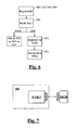
- FIG 7 illustrates schematically, as an example of application, a portable device HD in which the integrated circuit IC2 or IC3 is integrated.
- the HP portable device can be a smart card, a tag, a mobile phone, a PDA (personal digital assistant), etc.
- the integrated circuit IC2 or IC3 is connected to an antenna coil and is configured to exchange data and perform a transaction with an NFCD (Near Field Communication) external device such as a card or contactless tag reader, an NFC outlet, another NFC mobile phone, etc.
- NFCD Near Field Communication
Landscapes
- Engineering & Computer Science (AREA)
- Computer Security & Cryptography (AREA)
- Computer Networks & Wireless Communication (AREA)
- Signal Processing (AREA)
- Storage Device Security (AREA)
- Computer And Data Communications (AREA)
Applications Claiming Priority (1)
| Application Number | Priority Date | Filing Date | Title |
|---|---|---|---|
| FR0902205A FR2945366A1 (fr) | 2009-05-07 | 2009-05-07 | Circuit integre securise comprenant des moyens de divulgation de valeurs de masque de contre-mesure |
Publications (2)
| Publication Number | Publication Date |
|---|---|
| EP2249509A1 true EP2249509A1 (de) | 2010-11-10 |
| EP2249509B1 EP2249509B1 (de) | 2012-02-22 |
Family
ID=41727402
Family Applications (1)
| Application Number | Title | Priority Date | Filing Date |
|---|---|---|---|
| EP10004303A Ceased EP2249509B1 (de) | 2009-05-07 | 2010-04-22 | Gesicherte integrierte Schaltungsanordnung mit Mitteln zur Bekanntgabe von Maskierungswerten für Gegenmassnahmen |
Country Status (5)
| Country | Link |
|---|---|
| US (1) | US20100287386A1 (de) |
| EP (1) | EP2249509B1 (de) |
| AT (1) | ATE546908T1 (de) |
| CA (1) | CA2701433A1 (de) |
| FR (1) | FR2945366A1 (de) |
Families Citing this family (5)
| Publication number | Priority date | Publication date | Assignee | Title |
|---|---|---|---|---|
| WO2011121298A2 (en) * | 2010-03-31 | 2011-10-06 | British Telecommunications Public Limited Company | Secure data recorder |
| US10037522B2 (en) * | 2012-01-17 | 2018-07-31 | Raytheon Bbn Technologies Corp. | Near-field communication (NFC) system and method for private near-field communication |
| US9363276B2 (en) * | 2014-10-08 | 2016-06-07 | Corsec Security, Inc. | Method and system for testing and validation of cryptographic algorithms |
| ITUB20152708A1 (it) * | 2015-07-31 | 2017-01-31 | St Microelectronics Srl | Procedimento per operare una crittografia con mascheratura di dati sensibili, apparato di crittografia e prodotto informatico corrispondente |
| US12388622B2 (en) * | 2023-02-09 | 2025-08-12 | International Business Machines Corporation | Masking ciphertexts using random elements for secure decryption |
Citations (4)
| Publication number | Priority date | Publication date | Assignee | Title |
|---|---|---|---|---|
| US6278783B1 (en) * | 1998-06-03 | 2001-08-21 | Cryptography Research, Inc. | Des and other cryptographic, processes with leak minimization for smartcards and other cryptosystems |
| EP1329787A2 (de) * | 2002-01-16 | 2003-07-23 | Texas Instruments Incorporated | Anzeige des sicheren Moduses für intelligente Telefone und persönliche digitale Assistenten |
| EP1331539A2 (de) * | 2002-01-16 | 2003-07-30 | Texas Instruments France | Sicherer Modus für Prozessoren, die Speicherverwaltung und Unterbrechungen unterstützen |
| US20050138481A1 (en) * | 2003-12-19 | 2005-06-23 | International Business Machines Corporation | Microcomputer, A Method For Protecting Memory And A Method For Performing Debugging |
Family Cites Families (5)
| Publication number | Priority date | Publication date | Assignee | Title |
|---|---|---|---|---|
| US7861312B2 (en) * | 2000-01-06 | 2010-12-28 | Super Talent Electronics, Inc. | MP3 player with digital rights management |
| US6466048B1 (en) * | 2001-05-23 | 2002-10-15 | Mosaid Technologies, Inc. | Method and apparatus for switchably selecting an integrated circuit operating mode |
| JP2004213216A (ja) * | 2002-12-27 | 2004-07-29 | Renesas Technology Corp | 情報セキュリティマイクロコンピュータ、そのプログラム開発装置およびそれらを含んだプログラム開発システム |
| EP1646174A1 (de) * | 2004-10-07 | 2006-04-12 | Axalto SA | Verfahren und Vorrichtung zur automatischen Generierung eines Kryptographisch Instruktionsatz und Codegenerierung |
| US8111828B2 (en) * | 2007-07-31 | 2012-02-07 | Hewlett-Packard Development Company, L.P. | Management of cryptographic keys for securing stored data |
-
2009
- 2009-05-07 FR FR0902205A patent/FR2945366A1/fr active Pending
-
2010
- 2010-04-22 AT AT10004303T patent/ATE546908T1/de active
- 2010-04-22 EP EP10004303A patent/EP2249509B1/de not_active Ceased
- 2010-04-29 CA CA2701433A patent/CA2701433A1/fr not_active Abandoned
- 2010-05-07 US US12/775,678 patent/US20100287386A1/en not_active Abandoned
Patent Citations (4)
| Publication number | Priority date | Publication date | Assignee | Title |
|---|---|---|---|---|
| US6278783B1 (en) * | 1998-06-03 | 2001-08-21 | Cryptography Research, Inc. | Des and other cryptographic, processes with leak minimization for smartcards and other cryptosystems |
| EP1329787A2 (de) * | 2002-01-16 | 2003-07-23 | Texas Instruments Incorporated | Anzeige des sicheren Moduses für intelligente Telefone und persönliche digitale Assistenten |
| EP1331539A2 (de) * | 2002-01-16 | 2003-07-30 | Texas Instruments France | Sicherer Modus für Prozessoren, die Speicherverwaltung und Unterbrechungen unterstützen |
| US20050138481A1 (en) * | 2003-12-19 | 2005-06-23 | International Business Machines Corporation | Microcomputer, A Method For Protecting Memory And A Method For Performing Debugging |
Also Published As
| Publication number | Publication date |
|---|---|
| CA2701433A1 (fr) | 2010-11-07 |
| FR2945366A1 (fr) | 2010-11-12 |
| EP2249509B1 (de) | 2012-02-22 |
| ATE546908T1 (de) | 2012-03-15 |
| US20100287386A1 (en) | 2010-11-11 |
Similar Documents
| Publication | Publication Date | Title |
|---|---|---|
| US11876917B2 (en) | Authentication apparatus and method | |
| US11018847B2 (en) | Device keys protection | |
| DK2907067T3 (en) | Smartcard chip personalization method and system | |
| EP3152860B1 (de) | Verfahren zur authentifizierung einer ersten elektronischen einheit durch eine zweite elektronische einheit und dieses verfahren umsetzende elektronische einheit | |
| EP2463833A1 (de) | Verfahren und Vorrichtung zur Ausführungskontrolle für interne Funktionen und Funktionen von geschützten Anwendungen auf Mikrochipkarten von mobilen Endgeräten | |
| EP2249509B1 (de) | Gesicherte integrierte Schaltungsanordnung mit Mitteln zur Bekanntgabe von Maskierungswerten für Gegenmassnahmen | |
| EP3410334B1 (de) | Verfahren zur authentifizierung einer integrierten schaltungsvorrichtung | |
| FR2867635A1 (fr) | Procede de traitement de donnees securise, base notamment sur un algorithme cryptographique | |
| EP3327607A1 (de) | Datenüberprüfungsverfahren | |
| US20100250962A1 (en) | Electronic token comprising several microprocessors and method of managing command execution on several microprocessors | |
| EP2599256B1 (de) | Verfahren und vorrichtung zur randomisierung eines geheimschlüssels für den schutz vor angriffen durch zusatzkanäle | |
| FR3088452A1 (fr) | Procede de verification d'integrite d'une paire de cles cryptographiques et dispositif cryptographique | |
| FR3133684A1 (fr) | Procédé d’authentification d’un dispositif esclave par un dispositif hôte | |
| CN120639632A (zh) | 模型推理方法、模型加密方法及装置 | |
| JP2014120974A (ja) | 暗号トークンおよび暗号処理システム |
Legal Events
| Date | Code | Title | Description |
|---|---|---|---|
| PUAI | Public reference made under article 153(3) epc to a published international application that has entered the european phase |
Free format text: ORIGINAL CODE: 0009012 |
|
| AK | Designated contracting states |
Kind code of ref document: A1 Designated state(s): AT BE BG CH CY CZ DE DK EE ES FI FR GB GR HR HU IE IS IT LI LT LU LV MC MK MT NL NO PL PT RO SE SI SK SM TR |
|
| AX | Request for extension of the european patent |
Extension state: AL BA ME RS |
|
| 17P | Request for examination filed |
Effective date: 20110418 |
|
| RAP1 | Party data changed (applicant data changed or rights of an application transferred) |
Owner name: INSIDE SECURE |
|
| RIC1 | Information provided on ipc code assigned before grant |
Ipc: H04L 9/06 20060101AFI20110530BHEP Ipc: G06F 11/36 20060101ALI20110530BHEP |
|
| RIC1 | Information provided on ipc code assigned before grant |
Ipc: G01R 31/3185 20060101ALN20110726BHEP Ipc: H04L 9/06 20060101AFI20110726BHEP |
|
| GRAP | Despatch of communication of intention to grant a patent |
Free format text: ORIGINAL CODE: EPIDOSNIGR1 |
|
| GRAS | Grant fee paid |
Free format text: ORIGINAL CODE: EPIDOSNIGR3 |
|
| GRAA | (expected) grant |
Free format text: ORIGINAL CODE: 0009210 |
|
| AK | Designated contracting states |
Kind code of ref document: B1 Designated state(s): AT BE BG CH CY CZ DE DK EE ES FI FR GB GR HR HU IE IS IT LI LT LU LV MC MK MT NL NO PL PT RO SE SI SK SM TR |
|
| REG | Reference to a national code |
Ref country code: GB Ref legal event code: FG4D Free format text: NOT ENGLISH |
|
| REG | Reference to a national code |
Ref country code: CH Ref legal event code: EP |
|
| REG | Reference to a national code |
Ref country code: AT Ref legal event code: REF Ref document number: 546908 Country of ref document: AT Kind code of ref document: T Effective date: 20120315 |
|
| REG | Reference to a national code |
Ref country code: IE Ref legal event code: FG4D Free format text: LANGUAGE OF EP DOCUMENT: FRENCH |
|
| REG | Reference to a national code |
Ref country code: DE Ref legal event code: R096 Ref document number: 602010000871 Country of ref document: DE Effective date: 20120412 |
|
| REG | Reference to a national code |
Ref country code: NL Ref legal event code: VDEP Effective date: 20120222 |
|
| LTIE | Lt: invalidation of european patent or patent extension |
Effective date: 20120222 |
|
| PG25 | Lapsed in a contracting state [announced via postgrant information from national office to epo] |
Ref country code: IS Free format text: LAPSE BECAUSE OF FAILURE TO SUBMIT A TRANSLATION OF THE DESCRIPTION OR TO PAY THE FEE WITHIN THE PRESCRIBED TIME-LIMIT Effective date: 20120622 Ref country code: HR Free format text: LAPSE BECAUSE OF FAILURE TO SUBMIT A TRANSLATION OF THE DESCRIPTION OR TO PAY THE FEE WITHIN THE PRESCRIBED TIME-LIMIT Effective date: 20120222 Ref country code: NL Free format text: LAPSE BECAUSE OF FAILURE TO SUBMIT A TRANSLATION OF THE DESCRIPTION OR TO PAY THE FEE WITHIN THE PRESCRIBED TIME-LIMIT Effective date: 20120222 Ref country code: LT Free format text: LAPSE BECAUSE OF FAILURE TO SUBMIT A TRANSLATION OF THE DESCRIPTION OR TO PAY THE FEE WITHIN THE PRESCRIBED TIME-LIMIT Effective date: 20120222 Ref country code: NO Free format text: LAPSE BECAUSE OF FAILURE TO SUBMIT A TRANSLATION OF THE DESCRIPTION OR TO PAY THE FEE WITHIN THE PRESCRIBED TIME-LIMIT Effective date: 20120522 |
|
| PG25 | Lapsed in a contracting state [announced via postgrant information from national office to epo] |
Ref country code: LV Free format text: LAPSE BECAUSE OF FAILURE TO SUBMIT A TRANSLATION OF THE DESCRIPTION OR TO PAY THE FEE WITHIN THE PRESCRIBED TIME-LIMIT Effective date: 20120222 Ref country code: FI Free format text: LAPSE BECAUSE OF FAILURE TO SUBMIT A TRANSLATION OF THE DESCRIPTION OR TO PAY THE FEE WITHIN THE PRESCRIBED TIME-LIMIT Effective date: 20120222 Ref country code: GR Free format text: LAPSE BECAUSE OF FAILURE TO SUBMIT A TRANSLATION OF THE DESCRIPTION OR TO PAY THE FEE WITHIN THE PRESCRIBED TIME-LIMIT Effective date: 20120523 Ref country code: PT Free format text: LAPSE BECAUSE OF FAILURE TO SUBMIT A TRANSLATION OF THE DESCRIPTION OR TO PAY THE FEE WITHIN THE PRESCRIBED TIME-LIMIT Effective date: 20120622 |
|
| REG | Reference to a national code |
Ref country code: IE Ref legal event code: FD4D |
|
| REG | Reference to a national code |
Ref country code: AT Ref legal event code: MK05 Ref document number: 546908 Country of ref document: AT Kind code of ref document: T Effective date: 20120222 |
|
| PG25 | Lapsed in a contracting state [announced via postgrant information from national office to epo] |
Ref country code: CY Free format text: LAPSE BECAUSE OF FAILURE TO SUBMIT A TRANSLATION OF THE DESCRIPTION OR TO PAY THE FEE WITHIN THE PRESCRIBED TIME-LIMIT Effective date: 20120222 |
|
| BERE | Be: lapsed |
Owner name: INSIDE SECURE Effective date: 20120430 |
|
| PG25 | Lapsed in a contracting state [announced via postgrant information from national office to epo] |
Ref country code: PL Free format text: LAPSE BECAUSE OF FAILURE TO SUBMIT A TRANSLATION OF THE DESCRIPTION OR TO PAY THE FEE WITHIN THE PRESCRIBED TIME-LIMIT Effective date: 20120222 Ref country code: IE Free format text: LAPSE BECAUSE OF FAILURE TO SUBMIT A TRANSLATION OF THE DESCRIPTION OR TO PAY THE FEE WITHIN THE PRESCRIBED TIME-LIMIT Effective date: 20120222 Ref country code: DK Free format text: LAPSE BECAUSE OF FAILURE TO SUBMIT A TRANSLATION OF THE DESCRIPTION OR TO PAY THE FEE WITHIN THE PRESCRIBED TIME-LIMIT Effective date: 20120222 Ref country code: RO Free format text: LAPSE BECAUSE OF FAILURE TO SUBMIT A TRANSLATION OF THE DESCRIPTION OR TO PAY THE FEE WITHIN THE PRESCRIBED TIME-LIMIT Effective date: 20120222 Ref country code: CZ Free format text: LAPSE BECAUSE OF FAILURE TO SUBMIT A TRANSLATION OF THE DESCRIPTION OR TO PAY THE FEE WITHIN THE PRESCRIBED TIME-LIMIT Effective date: 20120222 Ref country code: SI Free format text: LAPSE BECAUSE OF FAILURE TO SUBMIT A TRANSLATION OF THE DESCRIPTION OR TO PAY THE FEE WITHIN THE PRESCRIBED TIME-LIMIT Effective date: 20120222 Ref country code: EE Free format text: LAPSE BECAUSE OF FAILURE TO SUBMIT A TRANSLATION OF THE DESCRIPTION OR TO PAY THE FEE WITHIN THE PRESCRIBED TIME-LIMIT Effective date: 20120222 Ref country code: SE Free format text: LAPSE BECAUSE OF FAILURE TO SUBMIT A TRANSLATION OF THE DESCRIPTION OR TO PAY THE FEE WITHIN THE PRESCRIBED TIME-LIMIT Effective date: 20120222 |
|
| PG25 | Lapsed in a contracting state [announced via postgrant information from national office to epo] |
Ref country code: IT Free format text: LAPSE BECAUSE OF FAILURE TO SUBMIT A TRANSLATION OF THE DESCRIPTION OR TO PAY THE FEE WITHIN THE PRESCRIBED TIME-LIMIT Effective date: 20120222 Ref country code: SK Free format text: LAPSE BECAUSE OF FAILURE TO SUBMIT A TRANSLATION OF THE DESCRIPTION OR TO PAY THE FEE WITHIN THE PRESCRIBED TIME-LIMIT Effective date: 20120222 Ref country code: MC Free format text: LAPSE BECAUSE OF NON-PAYMENT OF DUE FEES Effective date: 20120430 |
|
| PLBE | No opposition filed within time limit |
Free format text: ORIGINAL CODE: 0009261 |
|
| STAA | Information on the status of an ep patent application or granted ep patent |
Free format text: STATUS: NO OPPOSITION FILED WITHIN TIME LIMIT |
|
| 26N | No opposition filed |
Effective date: 20121123 |
|
| PG25 | Lapsed in a contracting state [announced via postgrant information from national office to epo] |
Ref country code: BE Free format text: LAPSE BECAUSE OF NON-PAYMENT OF DUE FEES Effective date: 20120430 Ref country code: AT Free format text: LAPSE BECAUSE OF FAILURE TO SUBMIT A TRANSLATION OF THE DESCRIPTION OR TO PAY THE FEE WITHIN THE PRESCRIBED TIME-LIMIT Effective date: 20120222 |
|
| PG25 | Lapsed in a contracting state [announced via postgrant information from national office to epo] |
Ref country code: MK Free format text: LAPSE BECAUSE OF FAILURE TO SUBMIT A TRANSLATION OF THE DESCRIPTION OR TO PAY THE FEE WITHIN THE PRESCRIBED TIME-LIMIT Effective date: 20120222 |
|
| REG | Reference to a national code |
Ref country code: DE Ref legal event code: R097 Ref document number: 602010000871 Country of ref document: DE Effective date: 20121123 |
|
| PG25 | Lapsed in a contracting state [announced via postgrant information from national office to epo] |
Ref country code: ES Free format text: LAPSE BECAUSE OF FAILURE TO SUBMIT A TRANSLATION OF THE DESCRIPTION OR TO PAY THE FEE WITHIN THE PRESCRIBED TIME-LIMIT Effective date: 20120602 |
|
| PG25 | Lapsed in a contracting state [announced via postgrant information from national office to epo] |
Ref country code: BG Free format text: LAPSE BECAUSE OF FAILURE TO SUBMIT A TRANSLATION OF THE DESCRIPTION OR TO PAY THE FEE WITHIN THE PRESCRIBED TIME-LIMIT Effective date: 20120522 Ref country code: MT Free format text: LAPSE BECAUSE OF FAILURE TO SUBMIT A TRANSLATION OF THE DESCRIPTION OR TO PAY THE FEE WITHIN THE PRESCRIBED TIME-LIMIT Effective date: 20120222 |
|
| REG | Reference to a national code |
Ref country code: FR Ref legal event code: CA Effective date: 20131112 |
|
| REG | Reference to a national code |
Ref country code: DE Ref legal event code: R081 Ref document number: 602010000871 Country of ref document: DE Owner name: INSIDE SECURE, FR Free format text: FORMER OWNER: INSIDE SECURE, AIX-EN-PROVENCE, FR Effective date: 20131111 |
|
| PG25 | Lapsed in a contracting state [announced via postgrant information from national office to epo] |
Ref country code: TR Free format text: LAPSE BECAUSE OF FAILURE TO SUBMIT A TRANSLATION OF THE DESCRIPTION OR TO PAY THE FEE WITHIN THE PRESCRIBED TIME-LIMIT Effective date: 20120222 |
|
| PG25 | Lapsed in a contracting state [announced via postgrant information from national office to epo] |
Ref country code: LU Free format text: LAPSE BECAUSE OF NON-PAYMENT OF DUE FEES Effective date: 20120422 Ref country code: SM Free format text: LAPSE BECAUSE OF FAILURE TO SUBMIT A TRANSLATION OF THE DESCRIPTION OR TO PAY THE FEE WITHIN THE PRESCRIBED TIME-LIMIT Effective date: 20120222 |
|
| PG25 | Lapsed in a contracting state [announced via postgrant information from national office to epo] |
Ref country code: HU Free format text: LAPSE BECAUSE OF FAILURE TO SUBMIT A TRANSLATION OF THE DESCRIPTION OR TO PAY THE FEE WITHIN THE PRESCRIBED TIME-LIMIT Effective date: 20100422 |
|
| REG | Reference to a national code |
Ref country code: CH Ref legal event code: PL |
|
| PG25 | Lapsed in a contracting state [announced via postgrant information from national office to epo] |
Ref country code: CH Free format text: LAPSE BECAUSE OF NON-PAYMENT OF DUE FEES Effective date: 20140430 Ref country code: LI Free format text: LAPSE BECAUSE OF NON-PAYMENT OF DUE FEES Effective date: 20140430 |
|
| REG | Reference to a national code |
Ref country code: FR Ref legal event code: PLFP Year of fee payment: 6 |
|
| REG | Reference to a national code |
Ref country code: FR Ref legal event code: CL Name of requester: FRANCE BREVETS, FR Effective date: 20151027 |
|
| REG | Reference to a national code |
Ref country code: FR Ref legal event code: PLFP Year of fee payment: 7 |
|
| PGFP | Annual fee paid to national office [announced via postgrant information from national office to epo] |
Ref country code: GB Payment date: 20160324 Year of fee payment: 7 |
|
| REG | Reference to a national code |
Ref country code: FR Ref legal event code: PLFP Year of fee payment: 8 |
|
| REG | Reference to a national code |
Ref country code: GB Ref legal event code: 732E Free format text: REGISTERED BETWEEN 20170615 AND 20170621 |
|
| GBPC | Gb: european patent ceased through non-payment of renewal fee |
Effective date: 20170422 |
|
| PG25 | Lapsed in a contracting state [announced via postgrant information from national office to epo] |
Ref country code: GB Free format text: LAPSE BECAUSE OF NON-PAYMENT OF DUE FEES Effective date: 20170422 |
|
| REG | Reference to a national code |
Ref country code: FR Ref legal event code: PLFP Year of fee payment: 9 |
|
| REG | Reference to a national code |
Ref country code: DE Ref legal event code: R081 Ref document number: 602010000871 Country of ref document: DE Owner name: VERIMATRIX, FR Free format text: FORMER OWNER: INSIDE SECURE, MEYREUIL, FR |
|
| PGFP | Annual fee paid to national office [announced via postgrant information from national office to epo] |
Ref country code: FR Payment date: 20220421 Year of fee payment: 13 |
|
| PGFP | Annual fee paid to national office [announced via postgrant information from national office to epo] |
Ref country code: DE Payment date: 20220628 Year of fee payment: 13 |
|
| REG | Reference to a national code |
Ref country code: DE Ref legal event code: R119 Ref document number: 602010000871 Country of ref document: DE |
|
| PG25 | Lapsed in a contracting state [announced via postgrant information from national office to epo] |
Ref country code: FR Free format text: LAPSE BECAUSE OF NON-PAYMENT OF DUE FEES Effective date: 20230430 Ref country code: DE Free format text: LAPSE BECAUSE OF NON-PAYMENT OF DUE FEES Effective date: 20231103 |