EP2249478A1 - Filter, branching filter, communication module, and communication equipment - Google Patents
Filter, branching filter, communication module, and communication equipment Download PDFInfo
- Publication number
- EP2249478A1 EP2249478A1 EP08711633A EP08711633A EP2249478A1 EP 2249478 A1 EP2249478 A1 EP 2249478A1 EP 08711633 A EP08711633 A EP 08711633A EP 08711633 A EP08711633 A EP 08711633A EP 2249478 A1 EP2249478 A1 EP 2249478A1
- Authority
- EP
- European Patent Office
- Prior art keywords
- filter
- connecting line
- line layer
- substrate
- layer
- Prior art date
- Legal status (The legal status is an assumption and is not a legal conclusion. Google has not performed a legal analysis and makes no representation as to the accuracy of the status listed.)
- Granted
Links
Images



Classifications
-
- H—ELECTRICITY
- H03—ELECTRONIC CIRCUITRY
- H03H—IMPEDANCE NETWORKS, e.g. RESONANT CIRCUITS; RESONATORS
- H03H9/00—Networks comprising electromechanical or electro-acoustic elements; Electromechanical resonators
- H03H9/02—Details
- H03H9/05—Holders or supports
- H03H9/0538—Constructional combinations of supports or holders with electromechanical or other electronic elements
- H03H9/0566—Constructional combinations of supports or holders with electromechanical or other electronic elements for duplexers
- H03H9/0571—Constructional combinations of supports or holders with electromechanical or other electronic elements for duplexers including bulk acoustic wave [BAW] devices
-
- H—ELECTRICITY
- H03—ELECTRONIC CIRCUITRY
- H03H—IMPEDANCE NETWORKS, e.g. RESONANT CIRCUITS; RESONATORS
- H03H9/00—Networks comprising electromechanical or electro-acoustic elements; Electromechanical resonators
- H03H9/02—Details
- H03H9/05—Holders or supports
- H03H9/0538—Constructional combinations of supports or holders with electromechanical or other electronic elements
- H03H9/0566—Constructional combinations of supports or holders with electromechanical or other electronic elements for duplexers
- H03H9/0576—Constructional combinations of supports or holders with electromechanical or other electronic elements for duplexers including surface acoustic wave [SAW] devices
-
- H—ELECTRICITY
- H03—ELECTRONIC CIRCUITRY
- H03H—IMPEDANCE NETWORKS, e.g. RESONANT CIRCUITS; RESONATORS
- H03H9/00—Networks comprising electromechanical or electro-acoustic elements; Electromechanical resonators
- H03H9/70—Multiple-port networks for connecting several sources or loads, working on different frequencies or frequency bands, to a common load or source
- H03H9/703—Networks using bulk acoustic wave devices
- H03H9/706—Duplexers
-
- H—ELECTRICITY
- H03—ELECTRONIC CIRCUITRY
- H03H—IMPEDANCE NETWORKS, e.g. RESONANT CIRCUITS; RESONATORS
- H03H9/00—Networks comprising electromechanical or electro-acoustic elements; Electromechanical resonators
- H03H9/70—Multiple-port networks for connecting several sources or loads, working on different frequencies or frequency bands, to a common load or source
- H03H9/72—Networks using surface acoustic waves
- H03H9/725—Duplexers
Definitions
- the present invention relates to a filter such as a high-frequency filter used for mobile communication equipment or radio equipment represented by a mobile phone. Also, the invention relates to a duplexer using such a filter. Also, the invention relates to a communication module and a communication device in which such a filter or duplexer is built.
- the mobile phone terminal itself is continuously demanded to achieve a reduction in size and thickness, and it is a situation that the reduction in size and thickness of a communication device mounted therein is eagerly demanded.
- a reduction in size and thickness of a component used for the communication device becomes essential, and a reduction in size and thickness of a high-frequency filter or duplexers as a principal part is eagerly desired.
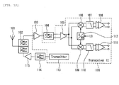
- Fig. 12 shows a configuration of a high-frequency block in a conventional mobile phone terminal.
- a reception path is connected with a inter-stage reception filter 104, and a transmission route is connected with a inter-stage transmission filter 114.
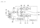
- a high-frequency block shown in Fig. 13 is configured such that the inter-stage transmission filter and the inter-stage reception filter are omitted for the purpose of simplifying the communication device.
- the inter-stage reception filter 104 was omitted, and an LNA 202 was provided in places of the LNAs 103 and 105. Also, on the transmission side, the inter-stage transmission filter 114 was omitted.
- the remaining filter element (duplexer 201) is demanded to have performances of the two conventional filter elements (inter-stage reception filter 104 and inter-stage transmission filter 114). Specifically, a great enhancement of out-of-band suppression, of the filter characteristic is demanded. Also, in addition to the above, a great enhancement of isolation between transmission and reception is demanded in the duplexer 201.
- An object of the invention is to provide a filter, a duplexer, a communication module and a communication device capable of suppressing unnecessary inductive and capacitive coupling in a substrate on which a filter element is mounted while realizing a reduction in size and thickness and having high suppression and high isolation characteristics.
- a first filter of the invention is a filter comprising a substrate and a filter element mounted on the substrate, wherein the substrate is provided with a plurality of connecting line layers including a connecting line layer for filter which is formed with transmission lines and connected with the filter element, an insulating layer formed at a position interposed between the plural connecting line layers and a ground pattern formed in at least a part of the lower connecting line layer of the connecting line layers for filter; and a thickness dimension of the insulating layer formed at a position interposed between the connecting line layer for filter and the other connecting line layer is smaller than a width dimension of the transmission line formed in the connecting line layer for filter and is larger than a thickness dimension of the other connecting line layer.
- a second filter of the invention is a filter comprising a substrate and a filter element mounted on the substrate, wherein the substrate is provided with a plurality of connecting line layers including a connecting line layer for filter which is formed with transmission lines and connected with the filter element, an insulating layer formed at a position interposed between the plural connecting line layers and a ground part formed in at least a part of the other connecting line layer under the connecting line layers for filter; and a thickness dimension of the insulating layer formed at a position interposed between the connecting line layer for filter and the other connecting line layer is smaller than a distance between the most neighboring transmission lines in the connecting line layer for filter and is larger than a thickness dimension of the other connecting line layer.
- the filter and a duplexer having high suppression and high isolation. Also, since an outermost surface insulating layer of the substrate is reduced in thickness, there gives rise to an effect for enabling the prepared filter and duplexer to achieve a reduction in size and thickness. Also, when mounted with such a filter or duplexer, it is possible to realize a reduction in size and thickness of a communication module or a communication device.
- a first filter of the invention is a filter comprising a substrate and a filter element mounted on the substrate, wherein the substrate is provided with a plurality of connecting line layers including a connecting line layer for filter which is formed with transmission lines and connected with the filter element, an insulating layer formed at a position interposed between the plural connecting line layers and a ground part formed in at least a part of the other connecting line layer under the connecting line layers for filter; and a thickness dimension of the insulating layer formed at a position interposed between the connecting line layer for filter and the other connecting line layer is smaller than a width dimension of the transmission line formed in the connecting line layer for filter and is larger than a thickness dimension of the other connecting line layer.
- a thickness dimension of the insulating layer formed at a position interposed between the connecting line layer for filter and the other connecting line layer is not more than 75 % of a width dimension of the transmission line formed in the connecting line layer for filter and is larger than a thickness dimension of the other connecting line layer. It is more desirable to take such a configuration, a partitioning ground as in the conventional technology is not necessary, and there gives rise to such an effect that a degree of freedom for design of the connecting line pattern increases, and therefore, such is more desirable.
- a second filter of the invention is a filter comprising a substrate and a filter element mounted on the substrate, wherein the substrate is provided with a plurality of connecting line layers including a connecting line layer for filter which is formed with transmission lines and connected with the filter element, an insulating layer formed at a position interposed between the plural connecting line layers and a ground part formed in at least a part of the other connecting line layer under the connecting line layers for filter; and a thickness dimension of the insulating layer formed at a position interposed between the connecting line layer for filter and the other connecting line layer is smaller than a distance between the most neighboring transmission lines in the connecting line layer for filter and is larger than a thickness dimension of the other connecting line layer.
- the outermost surface insulating layer as referred to herein is an insulating layer on which the filter is mounted.
- the filter of the invention can be configured such that the ground part is disposed in at least a part of a region directly under two transmission lines including the most neighboring part among the transmission lines formed in the connecting line layer for filter.
- the filter of the invention can be configured such that the ground part is disposed in at least a part of a region directly under the filter element in the other connecting line layer.
- the filter of the invention can be configured such that the ground part is disposed in at least a part of a region directly under a transmission line connected to a ground terminal of the filter element among the transmission lines formed in the connecting line layer for filter in the other connecting line layer.
- the filter of the invention can be configured such that the substrate is formed of a ceramic material.
- the ceramic material is small in dielectric loss tangent, and a loss of each of a high-frequency filter and a duplexer can be kept small. In consequence, it is possible to realize a high-frequency filter and a duplexer with high suppression in a low loss.
- the filter of the invention can be configured such that the substrate is formed of a resin material.
- the filter of the invention can be configured such that at least an outermost surface insulating layer in the substrate is formed of a resin material and that at least a part of the other insulating layer in the substrate is formed of a ceramic material.
- a resin material which is in general easier for achieving a reduction in thickness than a ceramic
- preparing the insulating layer other than the outermost surface insulating layer by using a ceramic having a characteristic feature that the dielectric loss tangent is small as compared with that of a resin, it is possible to prepare an insulating layer with small dielectric loss tangent. In consequence, advantages of the both materials can be effectively applied.
- the filter element is configured of an acoustic wave filter.
- the filter of the invention can be configured such that the filter element is mounted on the substrate by face down bonding.
- the filter of the invention can be configured such that the ground part is connected with a foot pattern for earth of the substrate by a plurality of vias between layers.
- the invention has a characteristic feature from the principal structural standpoint such that the ground pattern is disposed more closely to the connecting line pattern which generates the unnecessary coupling as compared with the conventional technology.
- Fig. 1A is a plan view showing a configuration of a filter according to an embodiment.
- Fig. 1B is a sectional view of a Z-Z part in Fig. 1A .
- the filter according to the present embodiment is provided with a substrate 1, a transmission line 2, a ground pattern 3, a bonding pad part 4 and a filter element 5.
- the ground pattern 3 is an example of the ground part of the invention.
- the substrate 1 is provided with a first insulating layer 11, a second insulating layer 12 and a third insulating layer 13.
- a first connecting line layer 14 is formed on the filter mounting surface in the first insulating layer 11.
- the first connecting line layer 14 according to the present embodiment is an example of the connecting line layer for filter of the invention.
- a second connecting line layer 15 is formed on the surface of the side of the first insulating layer 11 in the second insulating layer 12.
- the ground pattern 3 is arranged in at least a part of the second connecting line layer 15.
- a third connecting line layer 16 is formed on the surface of the side of the second insulating layer 12 in the third insulating layer 13.
- a fourth connecting line layer 17 is formed on the back surface relative to the surface on which the third connecting line layer 16 in the third insulating layer 13 is formed.
- the wiring 2 is arranged in via formed penetrating from the first connecting line layer 14 to the fourth connecting line layer 17 of the substrate 1 and electrically conducts the back and front of the substrate 1 to each other.
- the bonding pad part 4 is electrically connected to one end of the wiring 2 (end of the side of the first connecting line layer 14) and arranged.
- the filter element 5 is electrically connected to the bonding pad part 4 and arranged.
- the filter shown in Figs. 1A and 1B is configured such that the ground pattern 3 is disposed directly under the transmission line of the first connecting line layer 14 and that a thickness D2 of the first insulating layer 11 (outermost surface insulating layer) interposed between the first connecting line layer 14 and the second connecting line layer 15 positioning thereunder by one is thinner than a line width D1 of the wiring 2.
- the present embodiment is configured such that by arranging the ground pattern 3 in a lower portion of the first connecting line layer 14 (namely, disposing the transmission line and the ground pattern within a different plane from each other), the distance between the transmission line of the first connecting line layer 14 and the ground pattern 3 can be brought close to each other.
- the invention is characterized in that a high-frequency filter and a duplexer prepared using such a substrate 1 can be reduced in thickness as compared with conventional ones.
- Example of the filter of the invention is described with reference to a duplexer configured such that two filter elements are mounted on a low temperature co-fired ceramics (LTCC) substrate.
- this duplexer is a duplexer for Band 1 (transmission band: 1,920 to 1,980 MHz, reception band: 2, 110 to 2,170 MHz) of a third-generation mobile phone W-CDMA system.
- FIG. 2A shows a configuration of each of layers of the substrate of the prepared duplexer.
- FIG. 3 shows a sectional view of the substrate of the duplexer.
- a connecting line pattern 14a is formed in the first connecting line layer 14 on which the filter element 5 is mounted.
- the connecting line pattern 14a is provided with an antenna terminal 14b, a reception terminal 14c, a ground terminal 14d of a reception filter, a transmission terminal 14e and a ground terminal 14f of a reception filter.
- a ground pattern 15a for suppressing the unnecessary inductive and capacitive coupling is disposed in the second connecting line layer 15.
- This ground pattern 15a is corresponding to the ground pattern 3 shown in Figs. 1A and 1B .
- the ground pattern 15a is electrically connected to a ground 17d of a foot pattern in the fourth connecting line layer 17 shown in Fig. 2D with a plurality of vias between layers via the second connecting line layer 15 and the third connecting line layer 16 shown in Fig. 2C .
- the outermost surface insulating layer (first insulating layer 11) was set up at 25 ⁇ m. Also, a substrate whose thickness of the outermost surface insulating layer was set up at 100 ⁇ m was prepared for comparison. A thickness of each of the second insulating layer 12, the third insulating layer 13 and the fourth insulating layer 14 was set up at 100 ⁇ m. Also, those shown in Table 1 can be properly used as the insulating layer.
- Fig. 4 shows a mutual positional relation among the filter element 5, the connecting line pattern 14a of the first connecting line layer 14 and the ground pattern 15a of the second connecting line layer 15. Also, Fig. 4 shows a positional relation of the respective layers when seeing the substrate 1 in a normal line direction of its principal plane.
- the ground pattern 15a is disposed in the second conductor layer 15 over the substantially entire surface directly thereunder.
- the ground pattern 15a of the second conductor layer 15 is not disposed directly under a signal line connected to the transmission terminal 14e, and the ground pattern 15a is disposed in a region including one directly under the transmission line connected to other ground terminal (ground terminal 14d of the reception filter 41).
- a line width of the connecting line pattern is formed to be 100 ⁇ m, and a line/space is 100/100 ⁇ m as a design rule.
- Fig. 5 shows a circuit diagram of a duplexer.
- the reception filter 41 and the transmission filter 42 are configured in a ladder type filter in which FBAR filters are connected to each other in a ladder shape.
- Fig. 6 shows a configuration of a communication module provided with the duplexer according to the present embodiment.
- the communication module is provided with a duplexer 51, a low noise amplifier (LNA) 52 and a power amplifier (PA) 53.
- the duplexer 51 is configured of the duplexer according to the present embodiment.
- Fig. 7 shows a mounting configuration of the duplexer according to the present invention.
- the duplexer is provided with a phase matching circuit 62, a reception SAW filter 63 and a transmission SAW filter 64 on a substrate 61.
- the phase matching circuit 62 is connected to an antenna port 62a and also connected to each of the reception SWA filter 63 and the transmission SAW filter 64 via a transmission line 65 formed in the first connecting line layer 14 (see Fig. 1B ).
- the reception SAW filter 63 is connected to a reception port 63a via the transmission line 65 formed in the first connecting line layer 14.
- the transmission SAW filter 64 is connected to a transmission port 64a via the transmission line 65 formed in the first connecting line layer 14.
- a first ground pattern 66 is formed in the second connecting line layer 15 (see Fig. 1B ) and connected with the transmission port 64a.
- a second ground pattern 67 is formed in the third connecting line layer 16 (see Fig. 1B ) and connected with the antenna port 62a.
- a third ground pattern 68 is formed in the fourth connecting line layer 17 (see Fig. 1B ) and connected with the reception port 63a.
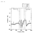
- Fig. 8 shows a transmission/reception characteristic in the duplexer shown in Fig. 5 .
- Fig. 9 shows isolation between the reception filter 41 and the reception filter 42 in the duplexer shown in Fig. 5 .
- the characteristics shown in Figs. 8 and 9 are the results obtained by measuring electrical characteristics using the duplexer shown in Fig. 5 .
- the duplexer used for the measurement there were prepared one in which the thickness of the outermost surface insulating layer (first insulating layer 11) of the filter was set up at 100 ⁇ m, a value of which is equal to the connecting line pattern width; and one in which the thickness of the outermost surface insulating layer (first insulating layer 11) was set up at 25 ⁇ m.
- the suppression level can be improved over a wide frequency band.
- the isolation of the transmission band can be reduced by 12 dB and that the isolation can be greatly improved.
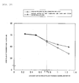
- Fig. 10 shows a change of the transmission band isolation relative to the thickness of the outermost surface insulating layer. Also, Fig. 10 shows the results obtained by calculating characteristics of the duplexer when a partitioning ground pattern was disposed while providing a gap of 100 ⁇ m between the connecting line patterns of the first connecting line layer 14, according to the electromagnetic field simulation. In this respect, the thickness of the outermost surface insulating layer (first insulating layer 11) was also changed.
- An abscissa of Fig. 10 represents a ratio of the thickness of the outermost surface insulating layer to the connecting line pattern width. As shown in Fig.
- the effect by the partitioning ground pattern vanishes, and thus, it was noted that the isolation is determined only by the effect of the ground pattern 3 formed in the second connecting line layer 15. Namely, it was noted that when the ratio of the thickness of the outermost surface insulating layer to the connecting line pattern width is not more than 0.75, the partitioning ground is not necessary and that there gives rise to such an effect that a degree of freedom for design of the connecting line pattern increases.
- Fig. 11 shows an RF block of a mobile phone terminal as an example of a communication device provided with the filter or duplexer according to the present embodiment.
- the configuration shown in Fig. 11 shows a configuration of a mobile phone terminal corresponding to a GSM (global system for mobile communications) communication system and a W-CDMA (wideband code division multiple access) communication system.
- the GSM communication system in the present embodiment is corresponding to an 850 MHz band, a 950 MHz band, a 1.8 GHz band and a 1. 9 GHz band, respectively.
- the mobile phone terminal is provided with a microphone, a speaker, a liquid crystal display and the like in addition to the configuration shown in Fig.
- the filter according to the present embodiment is included in each of reception filters 73a, 77, 78, 79 and 80 and a reception filter 73b.
- a duplexer 73 can be configured of the duplexer according to the present embodiment.
- LSI which is a subject of the action is chosen by an antenna switching circuit 72 depending upon whether the communication system is W-CDMA or GSM.
- switching is performed so as to output the received signal into the duplexer 73.
- the received signal inputted into the duplexer 73 is limited to a prescribed frequency band by the reception filter 73a, and a balance type received signal is outputted into an LNA 74.
- the LNA 74 amplifies the inputted received signal and outputs it into an LSI 76.
- the LSI 76 performs demodulation processing into an audio signal on the basis of the inputted received signal or performs action control of each of the components within the mobile phone terminal.
- the LSI 76 produces a transmitting signal.
- the produced transmitting is amplified by a power amplifier 75 and inputted into the transmission filter 73b.
- the transmission 73b allows only a signal of a prescribed frequency band among the inputted transmitting signal to pass therethrough.
- the transmitting signal outputted from the transmission 73b is outputted to the outside from the antenna 71 via the antenna switching circuit 72.
- the antenna switching circuit 72 chooses any one of the reception filters 77 to 80 depending upon the frequency band and outputs a received signal.
- the received signal whose band has been limited by any one of the reception filters 77 to 80 is inputted into an LSI 83.
- the LSI 83 performs demodulation processing into an audio signal on the basis of the inputted received signal or performs action control of each of the components within the mobile phone terminal.
- the LSI 83 produces a transmitting signal.
- the produced transmitting signal is amplified by a power amplifier 81 or 82 and outputted to the outside from the antenna 71 via the antenna switching circuit 72.
- the communication device with the filter or duplexer according to the present embodiment, not only the unnecessary inductive and capacitive coupling can be suppressed, but the isolation between reception and transmission can be enhanced. In consequence, the communication quality can be enhanced. Also, according to the present embodiment, since the outermost surface insulating layer (first insulating layer 11) is reduced in thickness, it is able to contribute to a reduction in thickness of a communication device.
- the thickness D2 of the outermost surface insulating layer (first insulating layer 11) thinner than the connecting line pattern width D1 and disposing the ground pattern 3 in the connecting line layer positioning thereunder by one as in the present embodiment, not only the unnecessary inductive and capacitive coupling can be suppressed, but the isolation between reception and transmission can be greatly improved.
- the outermost surface insulating layer (first insulating layer 11) is reduced in thickness, it is possible to achieve a reduction in size and thickness of a filter and a duplexer.
- a filter or duplexer By mounting such a filter or duplexer on a communication module or a communication device, it is possible to achieve a reduction in size and thickness of the communication module or communication device.
- the effect is obtained by making the thickness D2 of the outermost surface insulating layer (first insulating layer 11) thinner than a distance between the neighboringly disposed transmission lines. This is because in the case where the partitioning ground pattern cannot be disposed between the neighboring transmission lines, by making the thickness D2 of the outermost surface insulating layer (first insulating layer 11) thinner than the distance between the transmission lines and neighboringly disposing the ground pattern 3 of the second connecting line layer 15, the unnecessary inductive and capacitive coupling between transmission lines can be suppressed while facing the electromagnetic field radiations from the respective transmission lines toward the ground pattern 3.
- the ground pattern 3 disposed in the second connecting line layer 15 is disposed directly under of the transmission line of the first connecting line layer 14.
- the ground pattern 3 disposed in the second connecting line layer 15 is disposed directly under the transmission line having the most neighboring part in the first connecting line layer 14.
- the ground pattern 3 disposed in the second connecting line layer 15 is disposed directly under the filter element 5. This is because as shown in Fig. 1A , a plurality of the pads 4 for bonding the filter element 5 are present in the first connecting line layer 14 directly under the filter element 5; and the bonding pads 4 are disposed neighboringly each other, and they become a factor to cause the unnecessary inductive and capacitive coupling. In consequence, by disposing the ground pattern 3 directly under the filter element 5, the unnecessary inductive and capacitive coupling can be suppressed.
- the ground pattern 3 disposed in the second connecting line layer 15 is disposed directly under the transmission line connected to the ground terminal of the filter element 5 in the first connecting line layer 14. This is because when the ground pattern 3 is disposed neighboringly directly under the transmission line connected to the signal terminal of the filter element 5, the characteristic impedance of the transmission line changes and deteriorates a filter passing characteristic, whereas according to the configuration in which the ground pattern 3 is disposed directly under the transmission line connected to the ground terminal, the deterioration of a filter characteristic to be caused due to the impedance change is so small that it is negligible, and only the effect for suppressing the unnecessary inductive and capacitive coupling is obtainable.
- a material on which the filter is mounted is a ceramic.
- the ceramic material is small in dielectric loss tangent, and a loss of each of a high-frequency filter and a duplexer can be kept small. In consequence, it is possible to realize a high-frequency filter and a duplexer with high suppression in a low loss.
- a material of the substrate 1 may be a resin.
- the outermost surface insulating layer (first insulating layer 11) can be formed of a resin material, and the other insulating layer can be formed of a ceramic.
- the outermost surface insulating layer by forming the outermost surface insulating layer by using a resin which is in general easier to achieve a reduction in thickness than a ceramic, a thin outermost surface insulating layer can be easily prepared.
- the insulating layer other than the outermost surface insulating layer by using a ceramic having such a characteristic feature that the dielectric loss tangent is small as compared with that of a resin, it is possible to prepare an insulating layer with small dielectric loss tangent. In consequence, advantages of the both materials can be effectively applied.
- the filter element 5 can be configured of a surface acoustic wave filter (SWA filter) or a thin bulk acoustic resonator filter (FBAR filter). By taking such a configuration, it is possible to realize a small-sized high-frequency filter and a duplexer in a low loss.
- SWA filter surface acoustic wave filter
- FBAR filter thin bulk acoustic resonator filter
- the filter element 5 is mounted on the substrate 1 by face down bonding.
- the ground pattern 3 disposed in the second connecting line layer 15 is connected with a foot pattern for earth by a plurality of vias between layers. This is because a potential of the ground pattern 3 disposed in the second connecting line layer 15 becomes close to that of a true ground, and therefore, an electromagnetic field radiated from the transmission line of the first connecting line layer 14 advances more likely toward the ground pattern 3, and the unnecessary inductive and capacitive coupling between transmission lines can be suppressed.
- the filter, the duplexer, the communication module and the communication device of the invention are useful for equipment capable of receiving or transmitting a signal of a prescribed frequency.
Landscapes
- Physics & Mathematics (AREA)
- Acoustics & Sound (AREA)
- Surface Acoustic Wave Elements And Circuit Networks Thereof (AREA)
- Transceivers (AREA)
- Filters And Equalizers (AREA)
Abstract
Description
- The present invention relates to a filter such as a high-frequency filter used for mobile communication equipment or radio equipment represented by a mobile phone. Also, the invention relates to a duplexer using such a filter. Also, the invention relates to a communication module and a communication device in which such a filter or duplexer is built.
- In recent years, a multiband/multisystem advances for radio communication equipment represented by a mobile phone terminal, and a plurality of communication devices are mounted in one terminal. However, the mobile phone terminal itself is continuously demanded to achieve a reduction in size and thickness, and it is a situation that the reduction in size and thickness of a communication device mounted therein is eagerly demanded. Under such a background, a reduction in size and thickness of a component used for the communication device becomes essential, and a reduction in size and thickness of a high-frequency filter or duplexers as a principal part is eagerly desired.
- As another method for achieving a reduction in size of the communication device, there is a tendency to simplify the communication device and decrease the number of components used therein. For example,
Fig. 12 shows a configuration of a high-frequency block in a conventional mobile phone terminal. In the high-frequency block shown inFig. 12 , a reception path is connected with ainter-stage reception filter 104, and a transmission route is connected with ainter-stage transmission filter 114. On the other hand, a high-frequency block shown inFig. 13 is configured such that the inter-stage transmission filter and the inter-stage reception filter are omitted for the purpose of simplifying the communication device. In this respect, the high-frequency block shown inFig. 12 is provided with anantenna 101, aduplexer 102, a low noise amplifier (LNA) 103, ainter-stage reception filter 104, an LNA 105,mixers phase control circuit 112, atransmitter 113, ainter-stage transmission filter 114 and a power amplifier (PA) 115. Also, on the high-frequency block shown inFig. 13 , in the reception side, theinter-stage reception filter 104 was omitted, and an LNA 202 was provided in places of the LNAs 103 and 105. Also, on the transmission side, theinter-stage transmission filter 114 was omitted. - In this way, in the high-frequency block shown in
Fig. 13 , since the number of the filter elements is decreased, the remaining filter element (duplexer 201) is demanded to have performances of the two conventional filter elements (inter-stage reception filter 104 and inter-stage transmission filter 114). Specifically, a great enhancement of out-of-band suppression, of the filter characteristic is demanded. Also, in addition to the above, a great enhancement of isolation between transmission and reception is demanded in theduplexer 201. - In this way, in the high-frequency filter and duplexer used for a mobile phone terminal and the like, there was involved such a problem that the suppression level outside a pass-band and the isolation must be greatly enhanced while continuously advancing a reduction in size and thickness.
- As a factor to hinder the high suppression and high isolation of the filter and duplexer, there is exemplified unnecessary inductive and capacitive coupling generated in a substrate on which a filter element is mounted. Against this problem, for example, in a configuration disclosed in
Patent Document 1, in a mounted package on which a filter element is mounted, it was contrive to enhance a suppression level of the filter by disposing a ground pattern (partitioning ground pattern) for partitioning a plurality of transmission lines present in one connecting line layer between the transmission lines, thereby suppressing unnecessary inductive and capacitive coupling between the transmission lines. - Here, for the purpose of suppressing the unnecessary inductive and capacitive coupling between the transmission lines, in the case of disposing a ground pattern on the same connecting line layer as those transmission lines, it would be better to make the ground pattern close to the transmission lines as far as possible. This is because electromagnetic fields radiated from the respective transmission lines are surely induced into the partitioning ground pattern, whereby the inductive and capacitive coupling between the respective transmission lines is reduced.
- Patent Document 1:
JP-A-2008-180192 - However, for a gap between the transmission line and the partitioning ground pattern, the same degree as a line width had to be ensured (line/space = 1/1); there was a limit in suppressing the unnecessary inductive and capacitive coupling; a signal of the filter outside a pass-band could not be greatly suppressed; and the isolation between transmission and reception could not be greatly enhanced.
- An object of the invention is to provide a filter, a duplexer, a communication module and a communication device capable of suppressing unnecessary inductive and capacitive coupling in a substrate on which a filter element is mounted while realizing a reduction in size and thickness and having high suppression and high isolation characteristics.
- A first filter of the invention is a filter comprising a substrate and a filter element mounted on the substrate, wherein the substrate is provided with a plurality of connecting line layers including a connecting line layer for filter which is formed with transmission lines and connected with the filter element, an insulating layer formed at a position interposed between the plural connecting line layers and a ground pattern formed in at least a part of the lower connecting line layer of the connecting line layers for filter; and a thickness dimension of the insulating layer formed at a position interposed between the connecting line layer for filter and the other connecting line layer is smaller than a width dimension of the transmission line formed in the connecting line layer for filter and is larger than a thickness dimension of the other connecting line layer.
- A second filter of the invention is a filter comprising a substrate and a filter element mounted on the substrate, wherein the substrate is provided with a plurality of connecting line layers including a connecting line layer for filter which is formed with transmission lines and connected with the filter element, an insulating layer formed at a position interposed between the plural connecting line layers and a ground part formed in at least a part of the other connecting line layer under the connecting line layers for filter; and a thickness dimension of the insulating layer formed at a position interposed between the connecting line layer for filter and the other connecting line layer is smaller than a distance between the most neighboring transmission lines in the connecting line layer for filter and is larger than a thickness dimension of the other connecting line layer.
- According to the invention, it is possible to provide a filter and a duplexer having high suppression and high isolation. Also, since an outermost surface insulating layer of the substrate is reduced in thickness, there gives rise to an effect for enabling the prepared filter and duplexer to achieve a reduction in size and thickness. Also, when mounted with such a filter or duplexer, it is possible to realize a reduction in size and thickness of a communication module or a communication device.
-
-
Fig. 1A is a plan view of a filter according to an embodiment. -
Fig. 1B is a sectional view of a Z-Z part inFig. 1A . -
Fig. 2A is a plan view showing a configuration of a first connecting line layer in a substrate on which a filter element is mounted. -
Fig. 2B is a plan view showing a configuration of a second connecting line layer in a substrate on which a filter element is mounted. -
Fig. 2C is a plan view showing a configuration of a third connecting line layer in a substrate on which a filter element is mounted. -
Fig. 2D is a plan view showing a configuration of a fourth connecting line layer in a substrate on which a filter element is mounted. -
Fig. 3 is a sectional view of a substrate on which a filter element is mounted. -
Fig. 4 is a schematic view showing a state where a filter element and respective layers of a substrate are superimposed. -
Fig. 5 is a circuit diagram of a duplexer. -
Fig. 6 is a circuit diagram of a communication module using a duplexer of an embodiment. -
Fig. 7 is a plan view showing a configuration of a duplexer. -
Fig. 8 is a characteristic diagram showing frequency characteristics of a filter according to an embodiment and a conventional filter. -
Fig. 9 is a characteristic diagram showing frequency characteristics of a filter according to an embodiment and a conventional filter. -
Fig. 10 is a characteristic diagram showing a comparison of isolation by a disposal configuration of a ground pattern. -
Fig. 11 is a block diagram showing a configuration of a communication device according to an embodiment. -
Fig. 12 is a block diagram showing a configuration of a conventional high-frequency block. -
Fig. 13 is a block diagram showing a configuration of a high-frequency block in the future. - A first filter of the invention is a filter comprising a substrate and a filter element mounted on the substrate, wherein the substrate is provided with a plurality of connecting line layers including a connecting line layer for filter which is formed with transmission lines and connected with the filter element, an insulating layer formed at a position interposed between the plural connecting line layers and a ground part formed in at least a part of the other connecting line layer under the connecting line layers for filter; and a thickness dimension of the insulating layer formed at a position interposed between the connecting line layer for filter and the other connecting line layer is smaller than a width dimension of the transmission line formed in the connecting line layer for filter and is larger than a thickness dimension of the other connecting line layer. According to such a configuration, not only the unnecessary inductive and capacitive coupling can be suppressed, but the isolation between reception and transmission can be greatly improved.
- In the filter of the invention, it can be configured such that a thickness dimension of the insulating layer formed at a position interposed between the connecting line layer for filter and the other connecting line layer is not more than 75 % of a width dimension of the transmission line formed in the connecting line layer for filter and is larger than a thickness dimension of the other connecting line layer. It is more desirable to take such a configuration, a partitioning ground as in the conventional technology is not necessary, and there gives rise to such an effect that a degree of freedom for design of the connecting line pattern increases, and therefore, such is more desirable.
- A second filter of the invention is a filter comprising a substrate and a filter element mounted on the substrate, wherein the substrate is provided with a plurality of connecting line layers including a connecting line layer for filter which is formed with transmission lines and connected with the filter element, an insulating layer formed at a position interposed between the plural connecting line layers and a ground part formed in at least a part of the other connecting line layer under the connecting line layers for filter; and a thickness dimension of the insulating layer formed at a position interposed between the connecting line layer for filter and the other connecting line layer is smaller than a distance between the most neighboring transmission lines in the connecting line layer for filter and is larger than a thickness dimension of the other connecting line layer. By taking such a configuration, in the case where a partitioning ground pattern cannot be disposed between the neighboring transmission lines, by making a thickness of an outermost surface insulating layer thinner than a distance between the transmission lines and neighboringly disposing a ground pattern of the other connecting line layer, thereby facing electromagnetic field radiations from the respective transmission lines toward the ground pattern, the unnecessary inductive and capacitive coupling between transmission lines can be suppressed. In this respect, the outermost surface insulating layer as referred to herein is an insulating layer on which the filter is mounted.
- In the filter of the invention, it can be configured such that the ground part is disposed in at least a part of a region directly under two transmission lines including the most neighboring part among the transmission lines formed in the connecting line layer for filter. By taking such a configuration, electromagnetic fields radiated from the transmission lines of the connecting line layer for filter can be induced into the ground pattern directly thereunder, and radiation of the electromagnetic fields into surroundings can be suppressed.
- In the filter of the invention, it can be configured such that the ground part is disposed in at least a part of a region directly under the filter element in the other connecting line layer. By taking such a configuration, the unnecessary inductive and capacitive coupling can be suppressed.
- In the filter of the invention, it can be configured such that the ground part is disposed in at least a part of a region directly under a transmission line connected to a ground terminal of the filter element among the transmission lines formed in the connecting line layer for filter in the other connecting line layer. By taking such a configuration, the unnecessary inductive and capacitive coupling can be suppressed.
- In the filter of the invention, it can be configured such that the substrate is formed of a ceramic material. By taking such a configuration, it becomes easy to seal the
filter element 5 in an airtight manner. Furthermore, in general, the ceramic material is small in dielectric loss tangent, and a loss of each of a high-frequency filter and a duplexer can be kept small. In consequence, it is possible to realize a high-frequency filter and a duplexer with high suppression in a low loss. - In the filter of the invention, it can be configured such that the substrate is formed of a resin material. By taking such a configuration, in the case of mounting a plurality of filter elements on the substrate, even when the size of the substrate is large, it is possible to reduce a cost of the filter by using a resin-made printed wiring board.
- In the filter of the invention, it can be configured such that at least an outermost surface insulating layer in the substrate is formed of a resin material and that at least a part of the other insulating layer in the substrate is formed of a ceramic material. In this way, by forming the outermost surface insulating layer using a resin which is in general easier for achieving a reduction in thickness than a ceramic, it is possible to easily prepare a thin outermost surface insulating layer. Also, by preparing the insulating layer other than the outermost surface insulating layer by using a ceramic having a characteristic feature that the dielectric loss tangent is small as compared with that of a resin, it is possible to prepare an insulating layer with small dielectric loss tangent. In consequence, advantages of the both materials can be effectively applied.
- In the filter of the invention, the filter element is configured of an acoustic wave filter. By taking such a configuration, it is possible to realize a small-sized high-frequency filter and a duplexer in a low loss.
- In the filter of the invention, it can be configured such that the filter element is mounted on the substrate by face down bonding.
- In the filter of the invention, it can be configured such that the ground part is connected with a foot pattern for earth of the substrate by a plurality of vias between layers. By taking such a configuration, since a potential of the ground pattern disposed in the other connecting line layer becomes close to that of a true ground, an electromagnetic field radiated from the transmission line of the connecting line layer for filter advances more likely toward the ground pattern, and the unnecessary inductive and capacitive coupling between transmission lines can be suppressed.
- The invention has a characteristic feature from the principal structural standpoint such that the ground pattern is disposed more closely to the connecting line pattern which generates the unnecessary coupling as compared with the conventional technology.
-
Fig. 1A is a plan view showing a configuration of a filter according to an embodiment.Fig. 1B is a sectional view of a Z-Z part inFig. 1A . The filter according to the present embodiment is provided with asubstrate 1, atransmission line 2, aground pattern 3, abonding pad part 4 and afilter element 5. In this respect, theground pattern 3 is an example of the ground part of the invention. - The
substrate 1 is provided with a first insulatinglayer 11, a second insulatinglayer 12 and a third insulatinglayer 13. A first connectingline layer 14 is formed on the filter mounting surface in the first insulatinglayer 11. In this respect, the first connectingline layer 14 according to the present embodiment is an example of the connecting line layer for filter of the invention. A second connectingline layer 15 is formed on the surface of the side of the first insulatinglayer 11 in the second insulatinglayer 12. Also, theground pattern 3 is arranged in at least a part of the second connectingline layer 15. A third connectingline layer 16 is formed on the surface of the side of the second insulatinglayer 12 in the third insulatinglayer 13. Also, a fourth connectingline layer 17 is formed on the back surface relative to the surface on which the third connectingline layer 16 in the third insulatinglayer 13 is formed. - The
wiring 2 is arranged in via formed penetrating from the first connectingline layer 14 to the fourth connectingline layer 17 of thesubstrate 1 and electrically conducts the back and front of thesubstrate 1 to each other. Thebonding pad part 4 is electrically connected to one end of the wiring 2 (end of the side of the first connecting line layer 14) and arranged. Thefilter element 5 is electrically connected to thebonding pad part 4 and arranged. - For the purpose of suppressing the unnecessary inductive and capacitive coupling between transmission lines in the first connecting
line layer 14 disposed on the filter mounting surface, the filter shown inFigs. 1A and 1B is configured such that theground pattern 3 is disposed directly under the transmission line of the first connectingline layer 14 and that a thickness D2 of the first insulating layer 11 (outermost surface insulating layer) interposed between the first connectingline layer 14 and the second connectingline layer 15 positioning thereunder by one is thinner than a line width D1 of thewiring 2. - By taking such a configuration, in comparison with a configuration where a partitioning ground pattern is disposed within the same connecting line layer as in the conventional configuration, a distance between the transmission line in the first connecting
line layer 14 and theground pattern 3 can be shortened. This is because the ground pattern cannot be brought close to a level equal to or less than the line width within the same connecting line layer. That is, different from a conventional technology of arranging a transmission line and a ground pattern within the same plane, the present embodiment is configured such that by arranging theground pattern 3 in a lower portion of the first connecting line layer 14 (namely, disposing the transmission line and the ground pattern within a different plane from each other), the distance between the transmission line of the first connectingline layer 14 and theground pattern 3 can be brought close to each other. - In this respect, in order to keep electrical insulation between the first connecting
line layer 14 and the second connectingline layer 15, it is necessary that a lower limit of the thickness D2 of the first insulatinglayer 11 is larger than the thickness of the second connectingline layer 15. - Also, since the outermost surface insulating layer (first insulating layer 11) is reduced in thickness, the invention is characterized in that a high-frequency filter and a duplexer prepared using such a
substrate 1 can be reduced in thickness as compared with conventional ones. - Example of the filter of the invention is described with reference to a duplexer configured such that two filter elements are mounted on a low temperature co-fired ceramics (LTCC) substrate. In this respect, this duplexer is a duplexer for Band 1 (transmission band: 1,920 to 1,980 MHz, reception band: 2, 110 to 2,170 MHz) of a third-generation mobile phone W-CDMA system.
- Each of
Figs. 2A to 2D shows a configuration of each of layers of the substrate of the prepared duplexer.Fig. 3 shows a sectional view of the substrate of the duplexer. As shown inFig. 2A , a connectingline pattern 14a is formed in the first connectingline layer 14 on which thefilter element 5 is mounted. The connectingline pattern 14a is provided with anantenna terminal 14b, areception terminal 14c, aground terminal 14d of a reception filter, atransmission terminal 14e and aground terminal 14f of a reception filter. As shown inFig. 2B , aground pattern 15a for suppressing the unnecessary inductive and capacitive coupling is disposed in the second connectingline layer 15. Thisground pattern 15a is corresponding to theground pattern 3 shown inFigs. 1A and 1B . Theground pattern 15a is electrically connected to aground 17d of a foot pattern in the fourth connectingline layer 17 shown inFig. 2D with a plurality of vias between layers via the second connectingline layer 15 and the third connectingline layer 16 shown inFig. 2C . - In this respect, with respect to the thickness of the insulating layer, the outermost surface insulating layer (first insulating layer 11) was set up at 25 µm. Also, a substrate whose thickness of the outermost surface insulating layer was set up at 100 µm was prepared for comparison. A thickness of each of the second insulating
layer 12, the third insulatinglayer 13 and the fourth insulatinglayer 14 was set up at 100 µm. Also, those shown in Table 1 can be properly used as the insulating layer. -
[Table 1] Ceramic material Dielectric constant A 7 B 27 C 81 D 125 E 7.8 F 9 -
Fig. 4 shows a mutual positional relation among thefilter element 5, the connectingline pattern 14a of the first connectingline layer 14 and theground pattern 15a of the second connectingline layer 15. Also,Fig. 4 shows a positional relation of the respective layers when seeing thesubstrate 1 in a normal line direction of its principal plane. As shown inFig. 4 , in areception filter 41, theground pattern 15a is disposed in thesecond conductor layer 15 over the substantially entire surface directly thereunder. In atransmission filter 42, theground pattern 15a of thesecond conductor layer 15 is not disposed directly under a signal line connected to thetransmission terminal 14e, and theground pattern 15a is disposed in a region including one directly under the transmission line connected to other ground terminal (ground terminal 14d of the reception filter 41). In this respect, a line width of the connecting line pattern is formed to be 100 µm, and a line/space is 100/100 µm as a design rule. -
Fig. 5 shows a circuit diagram of a duplexer. Thereception filter 41 and thetransmission filter 42 are configured in a ladder type filter in which FBAR filters are connected to each other in a ladder shape. -
Fig. 6 shows a configuration of a communication module provided with the duplexer according to the present embodiment. The communication module is provided with aduplexer 51, a low noise amplifier (LNA) 52 and a power amplifier (PA) 53. Theduplexer 51 is configured of the duplexer according to the present embodiment. -
Fig. 7 shows a mounting configuration of the duplexer according to the present invention. As shown inFig. 7 , the duplexer is provided with aphase matching circuit 62, areception SAW filter 63 and atransmission SAW filter 64 on asubstrate 61. Thephase matching circuit 62 is connected to anantenna port 62a and also connected to each of thereception SWA filter 63 and thetransmission SAW filter 64 via atransmission line 65 formed in the first connecting line layer 14 (seeFig. 1B ). Thereception SAW filter 63 is connected to areception port 63a via thetransmission line 65 formed in the first connectingline layer 14. Thetransmission SAW filter 64 is connected to atransmission port 64a via thetransmission line 65 formed in the first connectingline layer 14. The duplexer shown inFig. 7 includes three kinds of different impedances (impedances of theantenna port 62a, thereception SAW filter 63 and the transmission SAW filter 64), and in the case of taking such a configuration, it is necessary to arrange a ground corresponding to each of the impedances. Afirst ground pattern 66 is formed in the second connecting line layer 15 (seeFig. 1B ) and connected with thetransmission port 64a. Asecond ground pattern 67 is formed in the third connecting line layer 16 (seeFig. 1B ) and connected with theantenna port 62a. Athird ground pattern 68 is formed in the fourth connecting line layer 17 (seeFig. 1B ) and connected with thereception port 63a. -
Fig. 8 shows a transmission/reception characteristic in the duplexer shown inFig. 5 .Fig. 9 shows isolation between thereception filter 41 and thereception filter 42 in the duplexer shown inFig. 5 . The characteristics shown inFigs. 8 and9 are the results obtained by measuring electrical characteristics using the duplexer shown inFig. 5 . As the duplexer used for the measurement, there were prepared one in which the thickness of the outermost surface insulating layer (first insulating layer 11) of the filter was set up at 100 µm, a value of which is equal to the connecting line pattern width; and one in which the thickness of the outermost surface insulating layer (first insulating layer 11) was set up at 25 µm. As a result of evaluating the respective duplexers, it was noted that as shown by the solid-line characteristics inFig. 8 , in the case of setting up the thickness of the outermost surface insulating layer at 25 µm, the suppression level can be improved over a wide frequency band. Also, as shown by the solid-line characteristics inFig. 9 , in particular, it was noted that the isolation of the transmission band can be reduced by 12 dB and that the isolation can be greatly improved. - In this respect, in the case of disposing the partitioning ground pattern in the same layer as the connecting line layer as in the conventional technology, since the suppression level and isolation are limited to the case where the distance between the connecting line pattern and the ground pattern is up to 100 µm, they are equal to the characteristics shown by the broken lines in
Figs. 8 and9 (characteristics when the thickness of the insulating layer is set up at 100 µm). -
Fig. 10 shows a change of the transmission band isolation relative to the thickness of the outermost surface insulating layer. Also,Fig. 10 shows the results obtained by calculating characteristics of the duplexer when a partitioning ground pattern was disposed while providing a gap of 100 µm between the connecting line patterns of the first connectingline layer 14, according to the electromagnetic field simulation. In this respect, the thickness of the outermost surface insulating layer (first insulating layer 11) was also changed. An abscissa ofFig. 10 represents a ratio of the thickness of the outermost surface insulating layer to the connecting line pattern width. As shown inFig. 10 , by regulating the ratio of the thickness of the outermost surface insulating layer to the connecting line pattern width to not more than 0.75, the effect by the partitioning ground pattern vanishes, and thus, it was noted that the isolation is determined only by the effect of theground pattern 3 formed in the second connectingline layer 15. Namely, it was noted that when the ratio of the thickness of the outermost surface insulating layer to the connecting line pattern width is not more than 0.75, the partitioning ground is not necessary and that there gives rise to such an effect that a degree of freedom for design of the connecting line pattern increases. -
Fig. 11 shows an RF block of a mobile phone terminal as an example of a communication device provided with the filter or duplexer according to the present embodiment. Also, the configuration shown inFig. 11 shows a configuration of a mobile phone terminal corresponding to a GSM (global system for mobile communications) communication system and a W-CDMA (wideband code division multiple access) communication system. Also, the GSM communication system in the present embodiment is corresponding to an 850 MHz band, a 950 MHz band, a 1.8 GHz band and a 1. 9 GHz band, respectively. Also, though the mobile phone terminal is provided with a microphone, a speaker, a liquid crystal display and the like in addition to the configuration shown inFig. 11 , since they are unnecessary in the explanation in the present embodiment, the illustration was omitted. Here, the filter according to the present embodiment is included in each ofreception filters reception filter 73b. Also, aduplexer 73 can be configured of the duplexer according to the present embodiment. - First of all, with respect to a received signal inputted via an
antenna 71, LSI which is a subject of the action is chosen by anantenna switching circuit 72 depending upon whether the communication system is W-CDMA or GSM. In the case where the inputted received signal is corresponding to the W-CDMA communication system, switching is performed so as to output the received signal into theduplexer 73. The received signal inputted into theduplexer 73 is limited to a prescribed frequency band by thereception filter 73a, and a balance type received signal is outputted into anLNA 74. TheLNA 74 amplifies the inputted received signal and outputs it into anLSI 76. TheLSI 76 performs demodulation processing into an audio signal on the basis of the inputted received signal or performs action control of each of the components within the mobile phone terminal. - On the other hand, in the case of transmitting a signal, the
LSI 76 produces a transmitting signal. The produced transmitting is amplified by apower amplifier 75 and inputted into thetransmission filter 73b. Thetransmission 73b allows only a signal of a prescribed frequency band among the inputted transmitting signal to pass therethrough. The transmitting signal outputted from thetransmission 73b is outputted to the outside from theantenna 71 via theantenna switching circuit 72. - Also, in the case where the inputted received signal is a signal corresponding to the GSM communication system, the
antenna switching circuit 72 chooses any one of the reception filters 77 to 80 depending upon the frequency band and outputs a received signal. The received signal whose band has been limited by any one of the reception filters 77 to 80 is inputted into anLSI 83. TheLSI 83 performs demodulation processing into an audio signal on the basis of the inputted received signal or performs action control of each of the components within the mobile phone terminal. On the other hand, in the case of transmitting a signal, theLSI 83 produces a transmitting signal. The produced transmitting signal is amplified by apower amplifier antenna 71 via theantenna switching circuit 72. - In the light of the above, by providing the communication device with the filter or duplexer according to the present embodiment, not only the unnecessary inductive and capacitive coupling can be suppressed, but the isolation between reception and transmission can be enhanced. In consequence, the communication quality can be enhanced. Also, according to the present embodiment, since the outermost surface insulating layer (first insulating layer 11) is reduced in thickness, it is able to contribute to a reduction in thickness of a communication device.
- By making the thickness D2 of the outermost surface insulating layer (first insulating layer 11) thinner than the connecting line pattern width D1 and disposing the
ground pattern 3 in the connecting line layer positioning thereunder by one as in the present embodiment, not only the unnecessary inductive and capacitive coupling can be suppressed, but the isolation between reception and transmission can be greatly improved. - Also, according to the present embodiment, since the outermost surface insulating layer (first insulating layer 11) is reduced in thickness, it is possible to achieve a reduction in size and thickness of a filter and a duplexer. By mounting such a filter or duplexer on a communication module or a communication device, it is possible to achieve a reduction in size and thickness of the communication module or communication device.
- Also, on the basis of the results of experiments made by the present inventors, as shown in
Fig. 10 , by regulating the thickness D2 of the outermost surface insulating layer (first insulating layer 11) to not more than 75 % of the line width D1 of thetransmission line 2, a partitioning ground pattern as in the conventional technology is not necessary, and there gives rise to such an effect that a degree of freedom for design of the connecting line pattern increases; and thus, such is more desirable. - Also, the effect is obtained by making the thickness D2 of the outermost surface insulating layer (first insulating layer 11) thinner than a distance between the neighboringly disposed transmission lines. This is because in the case where the partitioning ground pattern cannot be disposed between the neighboring transmission lines, by making the thickness D2 of the outermost surface insulating layer (first insulating layer 11) thinner than the distance between the transmission lines and neighboringly disposing the
ground pattern 3 of the second connectingline layer 15, the unnecessary inductive and capacitive coupling between transmission lines can be suppressed while facing the electromagnetic field radiations from the respective transmission lines toward theground pattern 3. - Also, it is desirable that the
ground pattern 3 disposed in the second connectingline layer 15 is disposed directly under of the transmission line of the first connectingline layer 14. By taking such a configuration, electromagnetic fields radiated from the transmission line of the connecting line layer forfilter 14 can be induced into theground pattern 3 directly thereunder, and radiation of the electromagnetic fields into surroundings can be suppressed. - Also, it is desirable that the
ground pattern 3 disposed in the second connectingline layer 15 is disposed directly under the transmission line having the most neighboring part in the first connectingline layer 14. By taking such a configuration, in the most neighboring part where the unnecessary inductive and capacitive coupling is the most remarkable, electromagnetic field radiations from the respective transmission lines can be induced into theground pattern 3 directly thereunder, and the inductive and capacitive coupling between transmission lines can be suppressed. - Also, it is desirable that the
ground pattern 3 disposed in the second connectingline layer 15 is disposed directly under thefilter element 5. This is because as shown inFig. 1A , a plurality of thepads 4 for bonding thefilter element 5 are present in the first connectingline layer 14 directly under thefilter element 5; and thebonding pads 4 are disposed neighboringly each other, and they become a factor to cause the unnecessary inductive and capacitive coupling. In consequence, by disposing theground pattern 3 directly under thefilter element 5, the unnecessary inductive and capacitive coupling can be suppressed. - Also, it is desirable that the
ground pattern 3 disposed in the second connectingline layer 15 is disposed directly under the transmission line connected to the ground terminal of thefilter element 5 in the first connectingline layer 14. This is because when theground pattern 3 is disposed neighboringly directly under the transmission line connected to the signal terminal of thefilter element 5, the characteristic impedance of the transmission line changes and deteriorates a filter passing characteristic, whereas according to the configuration in which theground pattern 3 is disposed directly under the transmission line connected to the ground terminal, the deterioration of a filter characteristic to be caused due to the impedance change is so small that it is negligible, and only the effect for suppressing the unnecessary inductive and capacitive coupling is obtainable. - Also, it is desirable that a material on which the filter is mounted is a ceramic. By taking such a configuration, it becomes easy to seal the
filter element 5 in an airtight manner. Furthermore, in general, the ceramic material is small in dielectric loss tangent, and a loss of each of a high-frequency filter and a duplexer can be kept small. In consequence, it is possible to realize a high-frequency filter and a duplexer with high suppression in a low loss. - Also, in the case of mounting a plurality of the
filter elements 5 on thesubstrate 1, a material of thesubstrate 1 may be a resin. By taking such a configuration, in the case of mounting a plurality of thefilter elements 5 on thesubstrate 1, even when the size of thesubstrate 1 is large, it is possible to reduce a cost of the filter by using a resin-made printed wiring board. - Also, in the
substrate 1 on which thefilter element 5 is mounted, the outermost surface insulating layer (first insulating layer 11) can be formed of a resin material, and the other insulating layer can be formed of a ceramic. In this way, by forming the outermost surface insulating layer by using a resin which is in general easier to achieve a reduction in thickness than a ceramic, a thin outermost surface insulating layer can be easily prepared. Also, by preparing the insulating layer other than the outermost surface insulating layer by using a ceramic having such a characteristic feature that the dielectric loss tangent is small as compared with that of a resin, it is possible to prepare an insulating layer with small dielectric loss tangent. In consequence, advantages of the both materials can be effectively applied. - Also, the
filter element 5 can be configured of a surface acoustic wave filter (SWA filter) or a thin bulk acoustic resonator filter (FBAR filter). By taking such a configuration, it is possible to realize a small-sized high-frequency filter and a duplexer in a low loss. - Also, it is desirable that the
filter element 5 is mounted on thesubstrate 1 by face down bonding. - Also, it is desirable that the
ground pattern 3 disposed in the second connectingline layer 15 is connected with a foot pattern for earth by a plurality of vias between layers. This is because a potential of theground pattern 3 disposed in the second connectingline layer 15 becomes close to that of a true ground, and therefore, an electromagnetic field radiated from the transmission line of the first connectingline layer 14 advances more likely toward theground pattern 3, and the unnecessary inductive and capacitive coupling between transmission lines can be suppressed. - The filter, the duplexer, the communication module and the communication device of the invention are useful for equipment capable of receiving or transmitting a signal of a prescribed frequency.
Claims (15)
- A filter comprising a substrate and a filter element mounted on the substrate, wherein
the substrate is provided with
a plurality of connecting line layers including a connecting line layer for filter which is formed with transmission lines and connected with the filter element,
an insulating layer interposed between the plural connecting line layers, and
a ground part formed in at least a part of the other connecting line layer under the connecting line layers for filter; and
a thickness dimension of the insulating layer interposed between the connecting line layer for filter and the other connecting line layer is smaller than a width dimension of the transmission line formed in the connecting line layer for filter and is larger than a thickness dimension of the other connecting line layer. - The filter according to claim 1, wherein
the thickness dimension of the insulating layer formed at a position interposed between the connecting line layer for filter and the other connecting line layer is not more than 75 % of the width dimension of the transmission line formed in the connecting line layer for filter and is larger than the thickness dimension of the other connecting line layer. - A filter comprising a substrate and a filter element mounted on the substrate, wherein
the substrate is provided with
a plurality of connecting line layers including a connecting line layer for filter which is formed with transmission lines and connected with the filter element,
an insulating layer formed at a position interposed between the plural connecting line layers, and
a ground part formed in at least a part of the other connecting line layer under the connecting line layers for filter; and
a thickness dimension of the insulating layer formed at a position interposed between the connecting line layer for filter and the other connecting line layer is smaller than a distance between the most neighboring transmission lines in the connecting line layer for filter and is larger than a thickness dimension of the other connecting line layer. - The filter according to claims 1 to 3, wherein
the ground part is disposed in at least a part of a region directly under two transmission lines including the most neighboring part among the transmission lines formed in the connecting line layer for filter. - The filter according to any one of claims 1 to 3, wherein
the ground part is disposed in at least a part of a region directly under the filter element in the other connecting line layer. - The filter according to any one of claims 1 to 3, wherein
the ground part is disposed in at least a part of a region directly under a transmission line connected to a ground terminal of the filter element among the transmission lines formed in the connecting line layer for filter in the other connecting line layer. - The filter according to any one of claims 1 to 6, wherein
the substrate is formed of a ceramic material. - The filter according to any one of claims 1 to 7, wherein
the substrate is formed of a resin material. - The filter according to any one of claims 1 to 7, wherein
at least an outermost surface insulating layer in the substrate is formed of a resin material; and
at least a part of other insulating layer in the substrate is formed of a ceramic material. - The filter according to any one of claims 1 to 9, wherein
the filter element is configured of an acoustic wave filter. - The filter according to claim 10, wherein
the filter element is mounted on the substrate by face down bonding. - The filter according to any one of claims 1 to 11, wherein
the ground part is connected with a foot pattern for earth of the substrate by a plurality of vias between layers. - A duplexer comprising the filter according to any one of claims 1 to 12.
- A communication module comprising the filter according to any one of claims 1 to 12 or the duplexer according to claim 13.
- A communication device comprising the communication module according to claim 14.
Applications Claiming Priority (1)
| Application Number | Priority Date | Filing Date | Title |
|---|---|---|---|
| PCT/JP2008/052827 WO2009104251A1 (en) | 2008-02-20 | 2008-02-20 | Filter, branching filter, communication module, and communication equipment |
Publications (3)
| Publication Number | Publication Date |
|---|---|
| EP2249478A1 true EP2249478A1 (en) | 2010-11-10 |
| EP2249478A4 EP2249478A4 (en) | 2011-03-23 |
| EP2249478B1 EP2249478B1 (en) | 2015-01-07 |
Family
ID=40985146
Family Applications (1)
| Application Number | Title | Priority Date | Filing Date |
|---|---|---|---|
| EP08711633.1A Not-in-force EP2249478B1 (en) | 2008-02-20 | 2008-02-20 | Filter, branching filter, communication module, and communication equipment |
Country Status (5)
| Country | Link |
|---|---|
| US (1) | US8367941B2 (en) |
| EP (1) | EP2249478B1 (en) |
| JP (1) | JP5583977B2 (en) |
| CN (1) | CN101953070B (en) |
| WO (1) | WO2009104251A1 (en) |
Families Citing this family (11)
| Publication number | Priority date | Publication date | Assignee | Title |
|---|---|---|---|---|
| JP5144379B2 (en) * | 2008-06-09 | 2013-02-13 | 太陽誘電株式会社 | Duplexer |
| CN102106083B (en) * | 2008-07-30 | 2015-11-25 | 京瓷株式会社 | Duplexer, communication module assembly and communication equipment |
| KR101350767B1 (en) * | 2010-04-28 | 2014-01-13 | 가부시키가이샤 무라타 세이사쿠쇼 | Circuit module |
| WO2011136100A1 (en) | 2010-04-30 | 2011-11-03 | 株式会社村田製作所 | Composite component |
| JP5603209B2 (en) * | 2010-11-10 | 2014-10-08 | 太陽誘電株式会社 | Demultiplexer and electronic device having the same |
| WO2012144228A1 (en) * | 2011-04-21 | 2012-10-26 | 株式会社村田製作所 | Circuit module |
| JP5618003B2 (en) * | 2011-06-21 | 2014-11-05 | 株式会社村田製作所 | Circuit module |
| JP6010292B2 (en) * | 2011-11-01 | 2016-10-19 | 太陽誘電株式会社 | Elastic wave device |
| CN104854792B (en) * | 2013-10-17 | 2018-11-06 | 株式会社村田制作所 | High-frequency circuit |
| JP5768951B1 (en) * | 2014-01-07 | 2015-08-26 | 株式会社村田製作所 | Filter device |
| JP2021164141A (en) * | 2020-04-03 | 2021-10-11 | 株式会社村田製作所 | High frequency module and communication device |
Family Cites Families (19)
| Publication number | Priority date | Publication date | Assignee | Title |
|---|---|---|---|---|
| JP3222072B2 (en) * | 1996-10-15 | 2001-10-22 | 富士通株式会社 | Demultiplexer package |
| US6483714B1 (en) * | 1999-02-24 | 2002-11-19 | Kyocera Corporation | Multilayered wiring board |
| US6743975B2 (en) * | 2001-03-19 | 2004-06-01 | Hewlett-Packard Development Company, L.P. | Low profile non-electrically-conductive component cover for encasing circuit board components to prevent direct contact of a conformal EMI shield |
| JP2002299917A (en) * | 2001-03-29 | 2002-10-11 | Kyocera Corp | High frequency transmission line |
| JP3649183B2 (en) * | 2001-12-27 | 2005-05-18 | ソニー株式会社 | Filter circuit device and manufacturing method thereof |
| JP2004166258A (en) * | 2002-10-25 | 2004-06-10 | Hitachi Metals Ltd | Balanced/unbalanced multiband filter module |
| WO2004038913A1 (en) * | 2002-10-25 | 2004-05-06 | Hitachi Metals, Ltd. | Balanced-unblanced type multi-band filer module |
| US7176383B2 (en) * | 2003-12-22 | 2007-02-13 | Endicott Interconnect Technologies, Inc. | Printed circuit board with low cross-talk noise |
| JP3778902B2 (en) * | 2003-04-28 | 2006-05-24 | 富士通メディアデバイス株式会社 | Duplexer and electronic device |
| WO2004107568A1 (en) * | 2003-06-03 | 2004-12-09 | Koninklijke Philips Electronics N.V. | Low pass filter and electronic device |
| JP2005151287A (en) | 2003-11-18 | 2005-06-09 | Tdk Corp | Electronic components |
| JP2005277522A (en) * | 2004-03-23 | 2005-10-06 | Tdk Corp | Electronic component |
| KR100633062B1 (en) * | 2004-10-07 | 2006-10-11 | 삼성전자주식회사 | 6-layer printed circuit board |
| JP4091043B2 (en) | 2004-12-22 | 2008-05-28 | 富士通メディアデバイス株式会社 | Duplexer |
| CN101395797B (en) * | 2006-03-08 | 2011-01-05 | 京瓷株式会社 | Signal splitter and communication device |
| US7613009B2 (en) * | 2006-03-15 | 2009-11-03 | Tdk Corporation | Electrical transition for an RF component |
| US8134084B2 (en) * | 2006-06-30 | 2012-03-13 | Shin-Etsu Polymer Co., Ltd. | Noise-suppressing wiring-member and printed wiring board |
| JP4729464B2 (en) * | 2006-09-20 | 2011-07-20 | ルネサスエレクトロニクス株式会社 | Directional coupler and high-frequency circuit module |
| JP2008180192A (en) | 2007-01-26 | 2008-08-07 | Nikki Co Ltd | Mounting structure of PTC heater in vaporizer |
-
2008
- 2008-02-20 WO PCT/JP2008/052827 patent/WO2009104251A1/en not_active Ceased
- 2008-02-20 JP JP2009554157A patent/JP5583977B2/en active Active
- 2008-02-20 CN CN200880127007.2A patent/CN101953070B/en active Active
- 2008-02-20 EP EP08711633.1A patent/EP2249478B1/en not_active Not-in-force
- 2008-02-20 US US12/918,781 patent/US8367941B2/en active Active
Also Published As
| Publication number | Publication date |
|---|---|
| US20100319975A1 (en) | 2010-12-23 |
| EP2249478A4 (en) | 2011-03-23 |
| WO2009104251A1 (en) | 2009-08-27 |
| JPWO2009104251A1 (en) | 2011-06-16 |
| CN101953070B (en) | 2015-03-25 |
| CN101953070A (en) | 2011-01-19 |
| US8367941B2 (en) | 2013-02-05 |
| JP5583977B2 (en) | 2014-09-03 |
| EP2249478B1 (en) | 2015-01-07 |
Similar Documents
| Publication | Publication Date | Title |
|---|---|---|
| EP2249478B1 (en) | Filter, branching filter, communication module, and communication equipment | |
| US8391821B2 (en) | Radio frequency circuit for multi-mode operation | |
| US10971459B2 (en) | High-frequency module | |
| US7941103B2 (en) | Duplexer | |
| US7053731B2 (en) | Duplexer using surface acoustic wave filters | |
| US8536957B1 (en) | High-frequency circuit module having a duplexer disposed between specified module integrated circuits | |
| US11043983B2 (en) | Radio frequency module and communication device including the same | |
| US11831299B2 (en) | High-frequency module and communication device | |
| US7663455B2 (en) | Band-pass filter element and high frequency module | |
| US11533806B2 (en) | High-frequency module, high-frequency circuit, and communication device | |
| US11418226B2 (en) | Radio frequency module and communication device | |
| US8159315B2 (en) | Substrate, communication module, and communication apparatus | |
| EP3968450B1 (en) | Wireless communication module | |
| US6996384B2 (en) | Receiver and radio communication terminal using the same | |
| US10749500B2 (en) | High-frequency module | |
| CN104602366B (en) | Communication module | |
| WO2013118664A1 (en) | High-frequency module | |
| US12155107B2 (en) | Filter, antenna module, and communication device | |
| US11303319B2 (en) | Radio frequency module and communication device | |
| US11418225B2 (en) | Radio frequency module and communication device | |
| JP2005136887A (en) | High frequency module and wireless communication device | |
| JP2006333127A (en) | High frequency filter parts, duplexers, high frequency modules and wireless communication devices |
Legal Events
| Date | Code | Title | Description |
|---|---|---|---|
| PUAI | Public reference made under article 153(3) epc to a published international application that has entered the european phase |
Free format text: ORIGINAL CODE: 0009012 |
|
| 17P | Request for examination filed |
Effective date: 20100819 |
|
| AK | Designated contracting states |
Kind code of ref document: A1 Designated state(s): AT BE BG CH CY CZ DE DK EE ES FI FR GB GR HR HU IE IS IT LI LT LU LV MC MT NL NO PL PT RO SE SI SK TR |
|
| AX | Request for extension of the european patent |
Extension state: AL BA MK RS |
|
| RIN1 | Information on inventor provided before grant (corrected) |
Inventor name: TSUTSUMI, JUN Inventor name: MATSUMOTO, KAZUHIRO |
|
| A4 | Supplementary search report drawn up and despatched |
Effective date: 20110223 |
|
| RIC1 | Information provided on ipc code assigned before grant |
Ipc: H04B 1/50 20060101ALI20110217BHEP Ipc: H03H 7/01 20060101AFI20090911BHEP Ipc: H03H 9/64 20060101ALI20110217BHEP Ipc: H03H 9/70 20060101ALI20110217BHEP Ipc: H05K 1/02 20060101ALI20110217BHEP Ipc: H03H 7/46 20060101ALI20110217BHEP Ipc: H03H 9/72 20060101ALI20110217BHEP |
|
| DAX | Request for extension of the european patent (deleted) | ||
| 17Q | First examination report despatched |
Effective date: 20130322 |
|
| REG | Reference to a national code |
Ref country code: DE Ref legal event code: R079 Ref document number: 602008036219 Country of ref document: DE Free format text: PREVIOUS MAIN CLASS: H03H0007010000 Ipc: H03H0009050000 |
|
| GRAP | Despatch of communication of intention to grant a patent |
Free format text: ORIGINAL CODE: EPIDOSNIGR1 |
|
| RIC1 | Information provided on ipc code assigned before grant |
Ipc: H03H 9/70 20060101ALI20140711BHEP Ipc: H03H 9/72 20060101ALI20140711BHEP Ipc: H03H 9/05 20060101AFI20140711BHEP |
|
| INTG | Intention to grant announced |
Effective date: 20140806 |
|
| GRAS | Grant fee paid |
Free format text: ORIGINAL CODE: EPIDOSNIGR3 |
|
| GRAA | (expected) grant |
Free format text: ORIGINAL CODE: 0009210 |
|
| AK | Designated contracting states |
Kind code of ref document: B1 Designated state(s): AT BE BG CH CY CZ DE DK EE ES FI FR GB GR HR HU IE IS IT LI LT LU LV MC MT NL NO PL PT RO SE SI SK TR |
|
| REG | Reference to a national code |
Ref country code: GB Ref legal event code: FG4D |
|
| REG | Reference to a national code |
Ref country code: CH Ref legal event code: EP |
|
| REG | Reference to a national code |
Ref country code: IE Ref legal event code: FG4D |
|
| REG | Reference to a national code |
Ref country code: AT Ref legal event code: REF Ref document number: 706343 Country of ref document: AT Kind code of ref document: T Effective date: 20150215 |
|
| REG | Reference to a national code |
Ref country code: DE Ref legal event code: R096 Ref document number: 602008036219 Country of ref document: DE Effective date: 20150219 |
|
| REG | Reference to a national code |
Ref country code: NL Ref legal event code: VDEP Effective date: 20150107 |
|
| REG | Reference to a national code |
Ref country code: AT Ref legal event code: MK05 Ref document number: 706343 Country of ref document: AT Kind code of ref document: T Effective date: 20150107 |
|
| REG | Reference to a national code |
Ref country code: LT Ref legal event code: MG4D |
|
| PG25 | Lapsed in a contracting state [announced via postgrant information from national office to epo] |
Ref country code: BE Free format text: LAPSE BECAUSE OF NON-PAYMENT OF DUE FEES Effective date: 20150228 |
|
| PG25 | Lapsed in a contracting state [announced via postgrant information from national office to epo] |
Ref country code: FI Free format text: LAPSE BECAUSE OF FAILURE TO SUBMIT A TRANSLATION OF THE DESCRIPTION OR TO PAY THE FEE WITHIN THE PRESCRIBED TIME-LIMIT Effective date: 20150107 Ref country code: NO Free format text: LAPSE BECAUSE OF FAILURE TO SUBMIT A TRANSLATION OF THE DESCRIPTION OR TO PAY THE FEE WITHIN THE PRESCRIBED TIME-LIMIT Effective date: 20150407 Ref country code: ES Free format text: LAPSE BECAUSE OF FAILURE TO SUBMIT A TRANSLATION OF THE DESCRIPTION OR TO PAY THE FEE WITHIN THE PRESCRIBED TIME-LIMIT Effective date: 20150107 Ref country code: HR Free format text: LAPSE BECAUSE OF FAILURE TO SUBMIT A TRANSLATION OF THE DESCRIPTION OR TO PAY THE FEE WITHIN THE PRESCRIBED TIME-LIMIT Effective date: 20150107 Ref country code: LT Free format text: LAPSE BECAUSE OF FAILURE TO SUBMIT A TRANSLATION OF THE DESCRIPTION OR TO PAY THE FEE WITHIN THE PRESCRIBED TIME-LIMIT Effective date: 20150107 Ref country code: SE Free format text: LAPSE BECAUSE OF FAILURE TO SUBMIT A TRANSLATION OF THE DESCRIPTION OR TO PAY THE FEE WITHIN THE PRESCRIBED TIME-LIMIT Effective date: 20150107 Ref country code: BG Free format text: LAPSE BECAUSE OF FAILURE TO SUBMIT A TRANSLATION OF THE DESCRIPTION OR TO PAY THE FEE WITHIN THE PRESCRIBED TIME-LIMIT Effective date: 20150407 |
|
| PG25 | Lapsed in a contracting state [announced via postgrant information from national office to epo] |
Ref country code: LV Free format text: LAPSE BECAUSE OF FAILURE TO SUBMIT A TRANSLATION OF THE DESCRIPTION OR TO PAY THE FEE WITHIN THE PRESCRIBED TIME-LIMIT Effective date: 20150107 Ref country code: GR Free format text: LAPSE BECAUSE OF FAILURE TO SUBMIT A TRANSLATION OF THE DESCRIPTION OR TO PAY THE FEE WITHIN THE PRESCRIBED TIME-LIMIT Effective date: 20150408 Ref country code: NL Free format text: LAPSE BECAUSE OF FAILURE TO SUBMIT A TRANSLATION OF THE DESCRIPTION OR TO PAY THE FEE WITHIN THE PRESCRIBED TIME-LIMIT Effective date: 20150107 Ref country code: AT Free format text: LAPSE BECAUSE OF FAILURE TO SUBMIT A TRANSLATION OF THE DESCRIPTION OR TO PAY THE FEE WITHIN THE PRESCRIBED TIME-LIMIT Effective date: 20150107 Ref country code: IS Free format text: LAPSE BECAUSE OF FAILURE TO SUBMIT A TRANSLATION OF THE DESCRIPTION OR TO PAY THE FEE WITHIN THE PRESCRIBED TIME-LIMIT Effective date: 20150507 Ref country code: PL Free format text: LAPSE BECAUSE OF FAILURE TO SUBMIT A TRANSLATION OF THE DESCRIPTION OR TO PAY THE FEE WITHIN THE PRESCRIBED TIME-LIMIT Effective date: 20150107 |
|
| REG | Reference to a national code |
Ref country code: CH Ref legal event code: PL |
|
| REG | Reference to a national code |
Ref country code: DE Ref legal event code: R097 Ref document number: 602008036219 Country of ref document: DE |
|
| PG25 | Lapsed in a contracting state [announced via postgrant information from national office to epo] |
Ref country code: MC Free format text: LAPSE BECAUSE OF FAILURE TO SUBMIT A TRANSLATION OF THE DESCRIPTION OR TO PAY THE FEE WITHIN THE PRESCRIBED TIME-LIMIT Effective date: 20150107 Ref country code: RO Free format text: LAPSE BECAUSE OF FAILURE TO SUBMIT A TRANSLATION OF THE DESCRIPTION OR TO PAY THE FEE WITHIN THE PRESCRIBED TIME-LIMIT Effective date: 20150107 Ref country code: LI Free format text: LAPSE BECAUSE OF NON-PAYMENT OF DUE FEES Effective date: 20150228 Ref country code: CH Free format text: LAPSE BECAUSE OF NON-PAYMENT OF DUE FEES Effective date: 20150228 Ref country code: CZ Free format text: LAPSE BECAUSE OF FAILURE TO SUBMIT A TRANSLATION OF THE DESCRIPTION OR TO PAY THE FEE WITHIN THE PRESCRIBED TIME-LIMIT Effective date: 20150107 Ref country code: DK Free format text: LAPSE BECAUSE OF FAILURE TO SUBMIT A TRANSLATION OF THE DESCRIPTION OR TO PAY THE FEE WITHIN THE PRESCRIBED TIME-LIMIT Effective date: 20150107 Ref country code: SK Free format text: LAPSE BECAUSE OF FAILURE TO SUBMIT A TRANSLATION OF THE DESCRIPTION OR TO PAY THE FEE WITHIN THE PRESCRIBED TIME-LIMIT Effective date: 20150107 Ref country code: EE Free format text: LAPSE BECAUSE OF FAILURE TO SUBMIT A TRANSLATION OF THE DESCRIPTION OR TO PAY THE FEE WITHIN THE PRESCRIBED TIME-LIMIT Effective date: 20150107 |
|
| PLBE | No opposition filed within time limit |
Free format text: ORIGINAL CODE: 0009261 |
|
| STAA | Information on the status of an ep patent application or granted ep patent |
Free format text: STATUS: NO OPPOSITION FILED WITHIN TIME LIMIT |
|
| REG | Reference to a national code |
Ref country code: IE Ref legal event code: MM4A |
|
| REG | Reference to a national code |
Ref country code: FR Ref legal event code: ST Effective date: 20151030 |
|
| 26N | No opposition filed |
Effective date: 20151008 |
|
| GBPC | Gb: european patent ceased through non-payment of renewal fee |
Effective date: 20150407 |
|
| PG25 | Lapsed in a contracting state [announced via postgrant information from national office to epo] |
Ref country code: IT Free format text: LAPSE BECAUSE OF FAILURE TO SUBMIT A TRANSLATION OF THE DESCRIPTION OR TO PAY THE FEE WITHIN THE PRESCRIBED TIME-LIMIT Effective date: 20150107 |
|
| PG25 | Lapsed in a contracting state [announced via postgrant information from national office to epo] |
Ref country code: GB Free format text: LAPSE BECAUSE OF NON-PAYMENT OF DUE FEES Effective date: 20150407 Ref country code: IE Free format text: LAPSE BECAUSE OF NON-PAYMENT OF DUE FEES Effective date: 20150220 |
|
| PG25 | Lapsed in a contracting state [announced via postgrant information from national office to epo] |
Ref country code: SI Free format text: LAPSE BECAUSE OF FAILURE TO SUBMIT A TRANSLATION OF THE DESCRIPTION OR TO PAY THE FEE WITHIN THE PRESCRIBED TIME-LIMIT Effective date: 20150107 Ref country code: FR Free format text: LAPSE BECAUSE OF NON-PAYMENT OF DUE FEES Effective date: 20150309 |
|
| PG25 | Lapsed in a contracting state [announced via postgrant information from national office to epo] |
Ref country code: BE Free format text: LAPSE BECAUSE OF FAILURE TO SUBMIT A TRANSLATION OF THE DESCRIPTION OR TO PAY THE FEE WITHIN THE PRESCRIBED TIME-LIMIT Effective date: 20150107 |
|
| PG25 | Lapsed in a contracting state [announced via postgrant information from national office to epo] |
Ref country code: MT Free format text: LAPSE BECAUSE OF FAILURE TO SUBMIT A TRANSLATION OF THE DESCRIPTION OR TO PAY THE FEE WITHIN THE PRESCRIBED TIME-LIMIT Effective date: 20150107 |
|
| PG25 | Lapsed in a contracting state [announced via postgrant information from national office to epo] |
Ref country code: HU Free format text: LAPSE BECAUSE OF FAILURE TO SUBMIT A TRANSLATION OF THE DESCRIPTION OR TO PAY THE FEE WITHIN THE PRESCRIBED TIME-LIMIT; INVALID AB INITIO Effective date: 20080220 |
|
| PG25 | Lapsed in a contracting state [announced via postgrant information from national office to epo] |
Ref country code: CY Free format text: LAPSE BECAUSE OF FAILURE TO SUBMIT A TRANSLATION OF THE DESCRIPTION OR TO PAY THE FEE WITHIN THE PRESCRIBED TIME-LIMIT Effective date: 20150107 |
|
| PG25 | Lapsed in a contracting state [announced via postgrant information from national office to epo] |
Ref country code: PT Free format text: LAPSE BECAUSE OF FAILURE TO SUBMIT A TRANSLATION OF THE DESCRIPTION OR TO PAY THE FEE WITHIN THE PRESCRIBED TIME-LIMIT Effective date: 20150507 |
|
| PG25 | Lapsed in a contracting state [announced via postgrant information from national office to epo] |
Ref country code: TR Free format text: LAPSE BECAUSE OF FAILURE TO SUBMIT A TRANSLATION OF THE DESCRIPTION OR TO PAY THE FEE WITHIN THE PRESCRIBED TIME-LIMIT Effective date: 20150107 |
|
| PG25 | Lapsed in a contracting state [announced via postgrant information from national office to epo] |
Ref country code: LU Free format text: LAPSE BECAUSE OF NON-PAYMENT OF DUE FEES Effective date: 20150220 |
|
| PGFP | Annual fee paid to national office [announced via postgrant information from national office to epo] |
Ref country code: DE Payment date: 20211230 Year of fee payment: 15 |
|
| P01 | Opt-out of the competence of the unified patent court (upc) registered |
Effective date: 20230509 |
|
| REG | Reference to a national code |
Ref country code: DE Ref legal event code: R119 Ref document number: 602008036219 Country of ref document: DE |
|
| PG25 | Lapsed in a contracting state [announced via postgrant information from national office to epo] |
Ref country code: DE Free format text: LAPSE BECAUSE OF NON-PAYMENT OF DUE FEES Effective date: 20230901 |