EP2249390A1 - Solid-state imaging device - Google Patents
Solid-state imaging device Download PDFInfo
- Publication number
- EP2249390A1 EP2249390A1 EP10735748A EP10735748A EP2249390A1 EP 2249390 A1 EP2249390 A1 EP 2249390A1 EP 10735748 A EP10735748 A EP 10735748A EP 10735748 A EP10735748 A EP 10735748A EP 2249390 A1 EP2249390 A1 EP 2249390A1
- Authority
- EP
- European Patent Office
- Prior art keywords
- register
- charge
- corner
- multiplication
- amplifier
- Prior art date
- Legal status (The legal status is an assumption and is not a legal conclusion. Google has not performed a legal analysis and makes no representation as to the accuracy of the status listed.)
- Granted
Links
Images




Classifications
-
- H—ELECTRICITY
- H10—SEMICONDUCTOR DEVICES; ELECTRIC SOLID-STATE DEVICES NOT OTHERWISE PROVIDED FOR
- H10F—INORGANIC SEMICONDUCTOR DEVICES SENSITIVE TO INFRARED RADIATION, LIGHT, ELECTROMAGNETIC RADIATION OF SHORTER WAVELENGTH OR CORPUSCULAR RADIATION
- H10F39/00—Integrated devices, or assemblies of multiple devices, comprising at least one element covered by group H10F30/00, e.g. radiation detectors comprising photodiode arrays
- H10F39/80—Constructional details of image sensors
-
- H—ELECTRICITY
- H04—ELECTRIC COMMUNICATION TECHNIQUE
- H04N—PICTORIAL COMMUNICATION, e.g. TELEVISION
- H04N25/00—Circuitry of solid-state image sensors [SSIS]; Control thereof
- H04N25/70—SSIS architectures; Circuits associated therewith
- H04N25/71—Charge-coupled device [CCD] sensors; Charge-transfer registers specially adapted for CCD sensors
- H04N25/713—Transfer or readout registers; Split readout registers or multiple readout registers
-
- H—ELECTRICITY
- H04—ELECTRIC COMMUNICATION TECHNIQUE
- H04N—PICTORIAL COMMUNICATION, e.g. TELEVISION
- H04N25/00—Circuitry of solid-state image sensors [SSIS]; Control thereof
- H04N25/70—SSIS architectures; Circuits associated therewith
- H04N25/71—Charge-coupled device [CCD] sensors; Charge-transfer registers specially adapted for CCD sensors
- H04N25/72—Charge-coupled device [CCD] sensors; Charge-transfer registers specially adapted for CCD sensors using frame transfer [FT]
-
- H—ELECTRICITY
- H10—SEMICONDUCTOR DEVICES; ELECTRIC SOLID-STATE DEVICES NOT OTHERWISE PROVIDED FOR
- H10D—INORGANIC ELECTRIC SEMICONDUCTOR DEVICES
- H10D44/00—Charge transfer devices
- H10D44/40—Charge-coupled devices [CCD]
- H10D44/45—Charge-coupled devices [CCD] having field effect produced by insulated gate electrodes
- H10D44/454—Output structures
-
- H—ELECTRICITY
- H10—SEMICONDUCTOR DEVICES; ELECTRIC SOLID-STATE DEVICES NOT OTHERWISE PROVIDED FOR
- H10F—INORGANIC SEMICONDUCTOR DEVICES SENSITIVE TO INFRARED RADIATION, LIGHT, ELECTROMAGNETIC RADIATION OF SHORTER WAVELENGTH OR CORPUSCULAR RADIATION
- H10F39/00—Integrated devices, or assemblies of multiple devices, comprising at least one element covered by group H10F30/00, e.g. radiation detectors comprising photodiode arrays
- H10F39/10—Integrated devices
- H10F39/12—Image sensors
- H10F39/15—Charge-coupled device [CCD] image sensors
- H10F39/158—Charge-coupled device [CCD] image sensors having arrangements for blooming suppression
Definitions
- the present invention relates to a charge multiplying solid-state imaging device.
- Non-Patent Literature 1 As a charge multiplying solid-state imaging device, one described in the following Non-Patent Literature 1 is known.
- the solid-state imaging device described in Non-Patent Literature 1 includes an imaging region, an output register, a corner register, a multiplication register, a first amplifier, an overscan element, and a second amplifier.
- This solid-state imaging device when multiplying a charge from the imaging region, transfers the charge from the imaging region in one direction by the output register, transfers the charge from the output register to the multiplication register via the corner register, multiplies the charge by the multiplication register, and outputs a signal based on the multiplied charge from the first amplifier.
- this solid-state imaging device when not multiplying a charge from the imaging region, transfers the charge from the imaging region in the other direction by the output register, transfers the charge from the output register by the overscan element, and outputs a signal based on the charge from the second amplifier.
- a dual-port solid-state imaging device includes an imaging region, an output register, a first corner register, a first multiplication register, a first amplifier, a second corner register, a second multiplication register, and a second amplifier.
- the imaging region is divided into first and second areas containing one or more pixel columns.
- This dual-port solid-state imaging device transfers a charge from the first area in one direction by the output register, transfers the charge to the first multiplication register via the first corner register, transfers the charge by the first multiplication register, and outputs a signal based on the multiplied charge from the first amplifier.
- this dual-port solid-state imaging device transfers a charge from the second area in the other direction by the output register, transfers the charge to the second multiplication register via the second corner register, multiplies the charge by the second multiplication register, and outputs a signal based on the multiplied charge from the second amplifier.
- this dual-port solid-state imaging device based on a charge from the whole area of the imaging region, can output a signal from one of the first and second amplifiers. For example, when outputting a signal from only the first amplifier, the dual-port solid-state imaging device transfers a charge from the whole area of the imaging region in one direction by the output register, transfers the charge to the first multiplication register via the first corner register, multiplies the charge by the first multiplication register, and outputs a signal based on the multiplied charge from the first amplifier.
- Non-Patent Literature 1 E2V CCD97-00 Black Illuminated 2-Phase IMO Series Electron Multiplying CCD Sensor Spec Sheet
- Non-Patent Literature 1 When outputting a charge from only one of the two amplifiers, may have produced noise.
- Non-Patent Literature 1 when outputting a signal from only the second amplifier, produces noise as a result of a charge from the unused corner register and multiplication register flowing into the output register.
- the inventor of the present application has also discovered that the foregoing multi-port charge multiplying solid-state imaging device, when outputting a signal from only one amplifier, produces noise as a result of a charge from an unused corner register and multiplication register flowing into the output register.
- the present invention has been made based on such knowledge.
- a solid-state imaging device of the present invention includes an imaging region, an output register, a corner register, a multiplication register, a first amplifier, a second amplifier, and a valve gate electrode.
- the output register is a transfer register that receives a charge transferred from the imaging region to transfer the charge.
- the output register is capable of selectively transferring a charge in one direction and in the other direction opposite to the one direction.
- the corner register transfers a charge transferred in one direction from the output register.
- the multiplication register receives the charge from the corner register and generates and transfers a multiplied charge.
- the first amplifier generates a signal based on the multiplied charge from the multiplication register.
- the second amplifier generates a signal based on a charge transferred in the other direction by the output register.
- the valve gate electrode is an electrode for preventing a transfer of a charge between the output register and the corner register.
- This solid-state imaging device by supplying voltage to the valve gate electrode when outputting a signal from the second amplifier, can prevent a charge from the unused corner register and multiplication register from flowing into the output register.
- the solid-state imaging device of the present invention further includes an overflow drain for discharging a charge accumulated in the corner register and the multiplication register.
- an overflow drain for discharging a charge accumulated in the corner register and the multiplication register.
- the solid-state imaging device of the present invention further includes an overscan element that is a register for transferring a charge transferred in the other direction from the output register to the second amplifier, and another valve gate electrode for preventing a transfer of a charge between the output register and the overscan element.
- an overscan element that is a register for transferring a charge transferred in the other direction from the output register to the second amplifier
- another valve gate electrode for preventing a transfer of a charge between the output register and the overscan element.
- Another solid-state imaging device of the present invention includes an imaging region, an output register, a first corner register, a first multiplication register, a first amplifier, a second corner register, a second multiplication register, a second amplifier, a first valve gate electrode, and a second valve gate electrode.
- the output register is a transfer register that receives a charge transferred from the imaging region to transfer the charge.
- the output register is capable of selectively transferring a charge in one direction and in the other direction opposite to the one direction.
- the first corner register transfers a charge transferred in one direction from the output register.
- the first multiplication register receives the charge from the first corner register and generates and transfers a multiplied charge.
- the first amplifier outputs a signal based on the multiplied charge from the first multiplication register.
- the second corner register transfers a charge transferred in the other direction from the output register.
- the second multiplication register receives the charge from the second corner register and generates and transfers a multiplied charge.
- a signal based on the multiplied charge from the second multiplication register is output.
- the first valve gate electrode is an electrode for preventing a transfer of a charge between the output register and the first corner register.
- the second valve gate electrode is an electrode for preventing a transfer of a charge between the output register and the second corner register.
- This solid-state imaging device allows, when outputting a signal from one of the first amplifier and the second amplifier, preventing a charge from the unused corner register and multiplication register from flowing into the output register by supplying voltage to a corresponding one of the first valve gate electrode and the second valve gate electrode.
- the solid-state imaging device of the present invention further includes an overflow drain for discharging a charge accumulated in the first and second corner registers and the first and second multiplication registers.
- an overflow drain for discharging a charge accumulated in the first and second corner registers and the first and second multiplication registers.
- a charge multiplying solid-state imaging device that is capable of reducing noise is provided.
- Fig. 1 is a view showing a solid-state imaging device according to an embodiment.
- Fig. 2 is a view showing with wiring the solid-state imaging device shown in Fig. 1 . Also, in Fig. 2 , an overflow drain to be described later is not shown.
- a solid-state imaging device 10 shown in Fig. 1 and Fig. 2 includes an imaging region 12, an output register 14, a corner register 16, a multiplication register 18, a first amplifier 20, a second amplifier 22, and a first valve gate electrode VG1. Moreover, the solid-state imaging device 10 may further include an overscan element 24, overflow drains 26a and 26b, and a second valve gate electrode VG2.
- the imaging region 12 is a region that generates a charge in response to incident light.
- the imaging region 12 includes a plurality of pixels arrayed two-dimensionally, and each pixel includes a photodiode.
- the solid-state imaging device 10 of the present embodiment includes a charge accumulating region 28 in addition to the imaging region 12.
- the charge accumulating region 28 is a section that temporarily accumulates a charge generated by the imaging region 12 before transferring the charge to an output register to be described later.
- the solid-state imaging device 10 having such a charge accumulating region 28 is called a frame transfer CCD image sensor.
- the solid-state imaging device of the present invention may be an interline CCD image sensor or a full-frame transfer CCD image sensor.
- the output register 14 is a transfer register that receives a charge generated by the imaging region 12 and then transferred in the vertical direction to transfer the charge in the horizontal direction.
- the output register 14 is capable of selectively transferring a charge in one direction X1 and the other direction X2 opposite to the one direction X1.
- the output register 14 transfers a charge as a result of receiving 3-phase clock signals supplied to terminals P1 to P3.
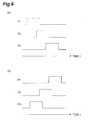
- the 3-phase clock signals are, in the case of transferring a charge in one direction X1, supplied in a partially overlapped manner to the terminals P1, P2, and P3 in this order (refer to (a) in Fig.
- the wirings extending from the terminals P1 to P3 are wirings common to the output register 14, the corner register 16, and the overscan element 24, and connected to the output register 14, the corner register 16, and the overscan element 24, respectively.
- the corner register 16 receives a charge transferred in the X1 direction from the output register 14, and transfers the charge further to the multiplication register 18. Specifically, the corner register 16 transfers a charge as a result of receiving the foregoing 3-phase clock signals.
- the multiplication register 18 is a register that multiplies a charge by an impact ionization effect, and transfers the multiplied charge.
- the multiplication register 18 receives a charge from the corner register 16 to generate a multiplied charge, and transfers the multiplied charge to the first amplifier 20.
- the multiplication register is connected with wirings extending from terminals PM1 to PM3 and PDC.
- the terminals PM1 to PM3 are terminals for inputting 3-phase clock signals to the multiplication register 18.
- the terminal PDC is a terminal that is input with a DC voltage for forming a barrier in the multiplication register 18.
- the first amplifier 20 receives a charge multiplied by the multiplication register 18 to perform charge-voltage conversion, and generates a signal according to the amount of charge received.
- a floating diffusion amplifier may be used as the first amplifier 20.
- the second amplifier 22 receives via the overscan element 24 a charge transferred in the other direction X2 by the output register 14, and outputs a signal according to the amount of charge.
- a floating diffusion amplifier may be used.
- the overscan element 24, like the output register 14, is a transfer register that, as a result of receiving 3-phase clock signals supplied to the terminals P1 to P3, transfers a charge to the second amplifier 22.
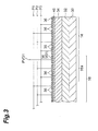
- Fig. 3 is a cross-sectional view along a line III-III of Fig. 2
- Fig. 4 is a cross-sectional view along a line IV-IV of Fig. 2 .
- the solid-state imaging device 10 includes a p-type substrate 30, a p-type epitaxial layer 32, an n-type region 34, and a plurality of electrodes 36.
- the p-type epitaxial layer 32 is provided on the p-type substrate 30, and the n-type region 34 is a region formed by doping from the top of the p-type epitaxial layer 32 an n-type dopant into a partial region of the layer 32.
- the electrodes 36 are provided above the n-type region 34 and on the dielectric layer 40.
- Each stage of the output register 14 and corner register 16 is configured with the p-type substrate 30, the p-type epitaxial layer 32, the n-type region 34, and three electrodes 36.
- the first valve gate electrode VG1 is an electrode that exists at the closest position to the output register 14 among the three electrodes 36 configuring a stage 16a of the corner register 16.
- the stage 16a is adjacent to the output register 14.
- the first valve gate electrode VG1 in the case of using the corner register 16, that is, when outputting a signal from the first amplifier 20, the same signal as a clock signal to be supplied to the terminal P1 out of the 3-phase clock signals is supplied.
- the first valve gate electrode VG1 is connected to a terminal PVG1 different from the terminal P1.
- a predetermined voltage is supplied to the first valve gate electrode VG1 from the terminal PVG1. Accordingly, a charge from the multiplication register 18 and corner register 16 is prevented from flowing into the output register 14.
- each stage of the overscan element 24 is also composed of the p-type substrate 30, the p-type epitaxial layer 32, the n-type region 34, and three electrodes 36.
- the second valve gate electrode VG2 is an electrode closest to the output register 14 among the three electrodes 36 configuring a stage 24a of the overscan element 24.
- the stage 24a is adjacent to the output register 14.
- the second valve gate electrode VG2 in the case of using the overscan element 24, that is, when outputting a signal from the second amplifier 22, the same signal as a clock signal to be supplied to the terminal P3 out of the 3-phase clock signals is supplied. However, the second valve gate electrode VG2 is connected to a terminal PVG2 different from the terminal P3. In the case of not using the overscan element 24, that is, when outputting a signal from the first amplifier 20, a predetermined voltage is supplied to the second valve gate electrode VG2 from the PVG2. Accordingly, a charge from the overscan element 24 is prevented from flowing in the output register 14.
- Fig. 5 is a cross-sectional view along a line V-V of Fig. 1 showing an example of an overflow drain.
- a p + -type channel stop layers 38 is formed at both sides of the n-type region 34.
- the dielectric layer 40 such as a SiO 2 layer is provided on the n-type region 34 and the channel stop layer 38.
- the overflow drain 26a is an n + -type semiconductor region, and provided along an edge of the n-type region 34.
- an overflow gate 42a is formed above the overflow drain 26a and on the dielectric layer 40.
- the overflow gate 42a and the electrode 36 are electrically separated by a dielectric layer 44.
- the overflow drain 26b is, like the overflow drain 26a, also provided along the n-type region 34 configuring the multiplication register 18, and an overflow gate 42b (not shown) is formed above the overflow drain 26b. To the overflow drain 26b, by supplying a predetermined voltage to the gate 42b, a charge accumulated in the multiplication register 18 is discharged.
- the overflow drain 26a and the gate 42a are provided along edges of the corner register 16, the output register 14, and the overscan element 24. Moreover, the overflow drain 26b and the gate 42b are separated from the overflow drain 26a and the gate 42a, and provided along the multiplication register 18.
- an n - -type semiconductor region 46 may be provided between the overflow drain 26a, 26b and the n-type region 34.
- the operation of the solid-state imaging device 10 when outputting a signal based on a charge from the imaging region 12 from the first amplifier 20, the charge from the imaging region 12 is transferred by the output register 14 in one direction X1. This charge is transferred to the multiplication register 18 via the corner register 16. Then, a multiplied charge is generated while being transferred by the multiplication register 18, and a signal based on the multiplied charge is generated by the first amplifier 20.
- a predetermined voltage is supplied from the terminal PVG2 to the second valve gate electrode VG2. Accordingly, an unnecessary charge from the unused overscan element 24 is prevented from flowing into the output register 14. As a result, noise in an output signal from the solid-state imaging device 10 is reduced.
- the charge from the imaging region 12 is transferred by the output register 14 in the other direction X2. This charge is further transferred by the overscan element 24. Then, a signal based on the charge from the overscan element 24 is generated by the second amplifier 22.
- a predetermined voltage is supplied from the terminal PVG1 to the first valve gate electrode VG1. Accordingly, an unnecessary charge from the unused corner register 16 and multiplication register 18 is prevented from flowing in the output register 14. As a result, noise in an output signal from the solid-state imaging device 10 is reduced.
- FIG. 7 is a view showing a solid-state imaging device according to another embodiment
- Fig. 8 is a view showing with wiring the solid-state imaging device shown in Fig. 7 .
- the solid-state imaging device 10A shown in Fig. 7 and Fig. 8 is a dual-port solid-state imaging device, and includes an imaging region 12A, an output register 14A, a first corner register 16 1 , a second corner register 16 2 , a first multiplication register 18 1 , a second multiplication register 18 2 , a first amplifier 20A, a second amplifier 22A, a first valve gate electrode VG1, and a second valve gate electrode VG2.
- the solid-state imaging device 10A may further include overflow drains 26a and 26b.
- the imaging region 12A is, like the imaging region 12 of the solid-state imaging device 10, a region that generates a charge in response to incident light.
- the imaging region 12A contains a first area 12 1 and a second area 12 2 .
- the first area 12 1 and the second area 12 2 are, in the figure, areas arranged side by side in the horizontal direction.
- the first area 12 1 and the second area 12 2 each contain a plurality of pixel columns.
- the solid-state imaging device 10A is also a frame transfer CCD image sensor including a charge accumulating region 28.
- the solid-state imaging device of the present invention may be an interline CCD image sensor or a full-frame transfer CCD image sensor.
- the output register 14A is a transfer register that transfers, in the horizontal direction, a charge transferred in the vertical direction from the imaging region 12A.
- the output register 14A can selectively transfer the charge from the imaging region 12A in one direction X1 and the other direction X2 opposite to the one direction X1.
- the output register 14A contains a first output register 14 1 and a second output register 14 2 .
- the first output register 14 1 is a transfer register that receives a charge from the first area 12 1
- the second output register 14 2 is a transfer register that receives a charge from the second area 12 2 .
- the first output register 14 1 is connected with wirings extending from terminals P1 1 , P2 1 , and P3 1 .
- the second output register 14 2 is connected with wirings extending from terminals P1 2 , P2 2 , and P3 2 .
- the first output register 14 1 as a result of 3-phase clock signals being supplied in a partially overlapped manner to the terminals P1 1 , P2 1 , and P3 1 in this order, transfers a charge in one direction X1.
- the first output register 14 1 as a result of 3-phase clock signals being supplied in a partially overlapped manner to the terminals P3 1 , P2 1 , and P1 1 in this order, transfers a charge in the other direction X2.
- the second output register 14 2 transfers a charge in the other direction X2. Moreover, the second output register 14 2 , as a result of 3-phase clock signals being supplied to the terminals P3 2 , P2 2 , and P1 2 in this order, transfers a charge in one direction X1.
- the first corner register 16 1 is a transfer register that transfers, to the first multiplication register 18 1 , a charge transferred from the output register 14A.
- the second corner register 16 2 is a register that transfers, to the second multiplication register 18 2 , a charge from the output register 14A.
- the wirings extending from the terminals P1 1 , P2 1 , and P3 1 are wirings common to the first output register 14 1 and the first corner register 16 1 , and connected also to the first corner register 16 1 .
- the wirings extending from the terminals P1 2 , P2 2 , and P3 2 are wirings common to the second output register 14 2 and the second corner register 16 2 , and connected also to the second corner register 16 2 .
- the first valve gate electrode VG1 in the solid-state imaging device 10A is an electrode closest to the output register 14A out of a plurality of electrodes that are included in a stage 16 1 a of the first corner register 16 1 that is adjacent to the output register 14A and to which clock signals are supplied.
- the first valve gate electrode VG1 is connected with a wiring from the terminal PVG1. In the case of transferring a charge by the first corner register 16 1 and outputting a signal from the first amplifier 20A, to the first valve gate electrode VG1, the same clock signal as a clock signal to be supplied from the terminal P1 1 is supplied from the terminal PVG1.
- the second valve gate electrode VG2 is an electrode closest to the output register 14A out of a plurality of electrodes that are included in a stage 16 2 a of the second corner register 16 2 that is adjacent to the output register 14A and to which clock signals are supplied.
- the second valve gate electrode VG2 is connected with a wiring from the terminal PVG2.
- the same clock signal as a clock signal to be supplied from the terminal P1 2 is supplied from the terminal PVG2.
- a predetermined voltage is supplied to the second valve gate electrode VG2 from the terminal PVG2. Accordingly, a charge is prevented from flowing in the output register 14A from the second corner register 16 2 .
- the first multiplication register 18 1 is a register that multiplies a charge by an impact ionization effect, and transfers the multiplied charge.
- the first multiplication register 18 1 receives a charge from the first corner register 16 1 to generate a multiplied charge, and transfers the multiplied charge to the first amplifier 20 1 .
- the first multiplication register 18 1 is connected with wirings extending from terminals PM1 1 , PDC 1 , PM2 1 , and PM3 1 .
- the terminals PM1 1 , PM2 1 , and PM3 1 are terminals for inputting 3-phase clock signals to the first multiplication register 18 1 .
- the terminal PDC 1 is a terminal that is input with a DC voltage for forming a barrier in the first multiplication register 18 1 .
- the first multiplication register 18 1 as a result of receiving signals input to these terminals PM1 1 , PDC 1 , PM2 1 , and PM3 1 , generates a multiplied charge, and transfers the charge.
- the second multiplication register 18 2 is also a register that multiplies a charge by an impact ionization effect, and transfers the multiplied charge.
- the second multiplication register 18 2 receives a charge from the second corner register 16 2 to generate a multiplied charge, and transfers the multiplied charge to the second amplifier 20 2 .
- the second multiplication register 18 2 is connected with wirings extending from terminals PM1 2 , PDC 2 , PM2 2 , and PM3 2 .
- the terminals PM1 2 , PM2 2 , and PM3 2 are terminals for inputting 3-phase clock signals to the second multiplication register 18 2 .
- the terminal PDC 2 is a terminal that is input with a DC voltage for forming a barrier in the second multiplication register 18 2 .
- the second multiplication register 18 2 as a result of receiving signals input to these terminals PM1 2 , PDC 2 , PM2 2 , and PM3 2 , generates a multiplied charge, and transfers the charge.
- the first amplifier 20A receives a charge multiplied by the first multiplication register 18 1 to perform charge-voltage conversion, and outputs a signal according to the amount of charge received.
- a floating diffusion amplifier may be used as the first amplifier 20A.
- the second amplifier 22A receives a charge multiplied by the second multiplication register 18 2 to perform charge-voltage conversion, and outputs a signal according to the amount of charge received.
- a floating diffusion amplifier may also be used for the second amplifier 22A.
- the overflow drain 26a is provided along edges of the output register 14A, the first corner register 16 1 , and the second corner register 16 2 .
- an overflow gate 42a is provided above the overflow drain 26a, as in the structure of the solid-state imaging device 10. This overflow drain 26a, as a result of a predetermined voltage being supplied to the overflow gate 42a, can discharge a charge from the output register 14A, the first corner register 16 1 , and the second corner register 16 2 .
- the overflow drain 26b is provided along each of the edges of the first multiplication register 18 1 and the second multiplication register 18 2 .
- an overflow gate 42b is provided above the overflow drain 26b. The overflow drain 26b, as a result of a predetermined voltage being supplied, can discharge a charge from the first multiplication register 18 1 and the second multiplication register 18 2 .
- an n - -type semiconductor region between the n-type semiconductor region and the overflow drain.
- the operation of the solid-state imaging device 10A when outputting signals from two ports, that is, when outputting signals from the first amplifier 20A and the second amplifier 22A, a charge from the first area 12 1 is transferred by the first output register 14 1 in one direction X1. Moreover, a charge from the second area 12 2 is transferred by the second output register 14 1 in the other direction X2.
- the charge from the first output register 14 1 is transferred to the first multiplication register 18 1 via the first corner register 16 1 .
- a multiplied charge is generated by the first multiplication register 18 1 .
- a signal based on the charge multiplied by the first multiplication register 18 1 is generated by the first amplifier 20A.
- the charge from the second output register 14 2 is transferred to the second multiplication register 18 2 via the second corner register 16 2 .
- a multiplied charge is generated and transferred by the second multiplication register 18 2 .
- a signal based on the charge multiplied by the second multiplication register 18 2 is generated by the second amplifier 22A.
- the solid-state imaging device 10A is capable of outputting signals at high speed.
- a charge from the whole area of the imaging region 12 is transferred by the output register 14A in one direction X1.
- the charge from the output register 14A is transferred to the first multiplication register 18 1 via the first corner register 16 1 .
- a multiplied charge is generated by the first multiplication register 18 1 .
- a signal based on the charge multiplied by the first multiplication register 18 1 is generated by the first amplifier 20A.
- a charge from the whole area of the imaging region 12 is transferred by the output register 14A in the other direction X2.
- the charge from the output register 14A is transferred to the second multiplication register 18 2 via the second corner register 16 2 .
- a multiplied charge is generated and transferred by the second multiplication register 18 2 .
- a signal based on the charge multiplied by the second multiplication register 18 2 is generated by the second amplifier 22A.
- the present invention is not limited to the foregoing embodiments, and can be variously modified.
- the solid-state imaging device of the foregoing embodiments are three-phase drive solid-state imaging devices, but the solid-state imaging device of the present invention may be a four-phase drive solid-state imaging device, and the number of phases of the clock signals to be input is by no means limited.
- the structure shown in Fig. 1 and the structure shown in Fig. 7 may be multi-ported.
- the solid-state imaging device of the present invention may include a plurality of units, each one of which is a structure containing the output register 14, the corner register 16, the multiplication register 18, the first amplifier 20, the second amplifier 22, and the first valve gate electrode VG1 of the solid-state imaging device 10.
- the output register of each unit transfers a charge from a corresponding pixel columns of the imaging region.
- the second valve gate VG2 the overscan element 24, and the overflow drains 26a and 26b may be included.
- the solid-state imaging device of the present invention may include a plurality of units, each one of which is a structure containing the output register 14, the corner registers 16 1 and 16 2 , the multiplication registers 18 1 and 18 2 , the amplifiers 20A and 22A, and the valve gate electrodes VG1 and VG2 of the solid-state imaging device 10A.
- the output register of each unit transfers a charge from a corresponding pixel columns of the imaging region.
- the overflow drains 26a and 26b may be included.
- the solid-state imaging device 10A shown in Fig. 7 is a dual-port solid-state imaging device
- the solid-state imaging device of the present invention may be a multi-port solid-state imaging device including a plurality of units, each one of which is a structure containing an output register that receives a charge from a corresponding pixel columns of the imaging region, a corner register that transfers the charge from the output register, a multiplication register that receives the charge from the corner register to generate a multiplied charge, an output register that generates a signal based on the multiplied charge from the multiplication register, and a valve gate electrode that prevents charge from flowing into the output register from the corner register.
- Second valve gate electrode, 10A Solid-state imaging device, 12A ... Imaging region, 12 1 ... First area, 12 2 ... Second area, 14A ... Output register, 14 1 ... First output register, 14 2 ... Second output register, 16 1 ... First corner register, 16 2 ... Second corner register, 18 1 ... First multiplication register, 18 2 ... Second multiplication register, 20A ... First amplifier, 22A ... Second amplifier, PI 1 , P2 1 , P3 1 , P1 2 , P2 2 , P3 2 , PM1 1 , PM2 1 , PM3 1 , PM1 2 , PM2 2 , PM3 2 , PDC 1 , PDC 2 ... Terminal.
Landscapes
- Engineering & Computer Science (AREA)
- Multimedia (AREA)
- Signal Processing (AREA)
- Solid State Image Pick-Up Elements (AREA)
- Transforming Light Signals Into Electric Signals (AREA)
Abstract
Description
- The present invention relates to a charge multiplying solid-state imaging device.
- As a charge multiplying solid-state imaging device, one described in the following Non-Patent
Literature 1 is known. The solid-state imaging device described in Non-PatentLiterature 1 includes an imaging region, an output register, a corner register, a multiplication register, a first amplifier, an overscan element, and a second amplifier. This solid-state imaging device, when multiplying a charge from the imaging region, transfers the charge from the imaging region in one direction by the output register, transfers the charge from the output register to the multiplication register via the corner register, multiplies the charge by the multiplication register, and outputs a signal based on the multiplied charge from the first amplifier. On the other hand, this solid-state imaging device, when not multiplying a charge from the imaging region, transfers the charge from the imaging region in the other direction by the output register, transfers the charge from the output register by the overscan element, and outputs a signal based on the charge from the second amplifier. - In addition, among charge multiplying solid-state imaging devices, there are multi-port solid-state imaging devices. For example, a dual-port solid-state imaging device includes an imaging region, an output register, a first corner register, a first multiplication register, a first amplifier, a second corner register, a second multiplication register, and a second amplifier. In the dual-port solid-state imaging device, the imaging region is divided into first and second areas containing one or more pixel columns. This dual-port solid-state imaging device transfers a charge from the first area in one direction by the output register, transfers the charge to the first multiplication register via the first corner register, transfers the charge by the first multiplication register, and outputs a signal based on the multiplied charge from the first amplifier. Simultaneously, this dual-port solid-state imaging device transfers a charge from the second area in the other direction by the output register, transfers the charge to the second multiplication register via the second corner register, multiplies the charge by the second multiplication register, and outputs a signal based on the multiplied charge from the second amplifier.
- Further, this dual-port solid-state imaging device, based on a charge from the whole area of the imaging region, can output a signal from one of the first and second amplifiers. For example, when outputting a signal from only the first amplifier, the dual-port solid-state imaging device transfers a charge from the whole area of the imaging region in one direction by the output register, transfers the charge to the first multiplication register via the first corner register, multiplies the charge by the first multiplication register, and outputs a signal based on the multiplied charge from the first amplifier.
- Non-Patent Literature 1: E2V CCD97-00 Black Illuminated 2-Phase IMO Series Electron Multiplying CCD Sensor Spec Sheet
- The charge multiplying solid-state imaging device described in
Non-Patent Literature 1 or the foregoing multi-port charge multiplying solid-state imaging device, when outputting a charge from only one of the two amplifiers, may have produced noise. - It is an object of the present invention to provide a charge multiplying solid-state imaging device that is capable of reducing noise.
- The inventor of the present application has discovered that the charge multiplying solid-state imaging device described in
Non-Patent Literature 1, when outputting a signal from only the second amplifier, produces noise as a result of a charge from the unused corner register and multiplication register flowing into the output register. The inventor of the present application has also discovered that the foregoing multi-port charge multiplying solid-state imaging device, when outputting a signal from only one amplifier, produces noise as a result of a charge from an unused corner register and multiplication register flowing into the output register. The present invention has been made based on such knowledge. - A solid-state imaging device of the present invention includes an imaging region, an output register, a corner register, a multiplication register, a first amplifier, a second amplifier, and a valve gate electrode. The output register is a transfer register that receives a charge transferred from the imaging region to transfer the charge. The output register is capable of selectively transferring a charge in one direction and in the other direction opposite to the one direction. The corner register transfers a charge transferred in one direction from the output register. The multiplication register receives the charge from the corner register and generates and transfers a multiplied charge. The first amplifier generates a signal based on the multiplied charge from the multiplication register. The second amplifier generates a signal based on a charge transferred in the other direction by the output register. The valve gate electrode is an electrode for preventing a transfer of a charge between the output register and the corner register.
- This solid-state imaging device, by supplying voltage to the valve gate electrode when outputting a signal from the second amplifier, can prevent a charge from the unused corner register and multiplication register from flowing into the output register.
- It is preferable that the solid-state imaging device of the present invention further includes an overflow drain for discharging a charge accumulated in the corner register and the multiplication register. As a result of discharging a charge accumulated in the corner register and the multiplication register by the overflow drain, the influence of a charge from the unused corner register and multiplication register on other elements is reduced.
- It is preferable that the solid-state imaging device of the present invention further includes an overscan element that is a register for transferring a charge transferred in the other direction from the output register to the second amplifier, and another valve gate electrode for preventing a transfer of a charge between the output register and the overscan element. This configuration allows, by supplying voltage to the other valve gate electrode when outputting a signal from the first amplifier, preventing a charge from the overscan element from flowing into the output register.
- Another solid-state imaging device of the present invention includes an imaging region, an output register, a first corner register, a first multiplication register, a first amplifier, a second corner register, a second multiplication register, a second amplifier, a first valve gate electrode, and a second valve gate electrode. The output register is a transfer register that receives a charge transferred from the imaging region to transfer the charge. The output register is capable of selectively transferring a charge in one direction and in the other direction opposite to the one direction. The first corner register transfers a charge transferred in one direction from the output register. The first multiplication register receives the charge from the first corner register and generates and transfers a multiplied charge. The first amplifier outputs a signal based on the multiplied charge from the first multiplication register. The second corner register transfers a charge transferred in the other direction from the output register. The second multiplication register receives the charge from the second corner register and generates and transfers a multiplied charge. A signal based on the multiplied charge from the second multiplication register is output. The first valve gate electrode is an electrode for preventing a transfer of a charge between the output register and the first corner register. The second valve gate electrode is an electrode for preventing a transfer of a charge between the output register and the second corner register.
- This solid-state imaging device allows, when outputting a signal from one of the first amplifier and the second amplifier, preventing a charge from the unused corner register and multiplication register from flowing into the output register by supplying voltage to a corresponding one of the first valve gate electrode and the second valve gate electrode.
- Moreover, it is preferable that the solid-state imaging device of the present invention further includes an overflow drain for discharging a charge accumulated in the first and second corner registers and the first and second multiplication registers. As a result of discharging a charge by the overflow drain, the influence of a charge from the unused corner register and multiplication register on other elements is reduced.
- As has been described above, according to the present invention, because a charge from the unused corner register and multiplication register can be prevented from flowing into the output register, a charge multiplying solid-state imaging device that is capable of reducing noise is provided.
-
-
Fig. 1 is a view showing a solid-state imaging device according to an embodiment. -
Fig. 2 is a view showing with wiring the solid-state imaging device shown inFig. 1 . -
Fig. 3 is a cross-sectional view along a line III-III ofFig. 2 . -
Fig. 4 is a cross-sectional view along a line IV-IV ofFig. 2 . -
Fig. 5 is a cross-sectional view along a line V-V ofFig. 1 showing an example of an overflow drain. -
Fig. 6 is a cross-sectional view showing another example of an overflow drain. -
Fig. 7 is a view showing a solid-state imaging device according to another embodiment. -
Fig. 8 is a view showing with wiring the solid-state imaging device shown inFig. 7 . -
Figs. 9 are diagrams showing examples of 3-phase clock signals. - Hereinafter, a preferred embodiment of the present invention will be described in detail with reference to the drawings. Also, the same or corresponding parts will be denoted with the same reference numerals in the drawings.
-
Fig. 1 is a view showing a solid-state imaging device according to an embodiment.Fig. 2 is a view showing with wiring the solid-state imaging device shown inFig. 1 . Also, inFig. 2 , an overflow drain to be described later is not shown. - A solid-
state imaging device 10 shown inFig. 1 andFig. 2 includes animaging region 12, anoutput register 14, acorner register 16, amultiplication register 18, afirst amplifier 20, asecond amplifier 22, and a first valve gate electrode VG1. Moreover, the solid-state imaging device 10 may further include anoverscan element 24, overflow drains 26a and 26b, and a second valve gate electrode VG2. - The
imaging region 12 is a region that generates a charge in response to incident light. Specifically, theimaging region 12 includes a plurality of pixels arrayed two-dimensionally, and each pixel includes a photodiode. - The solid-
state imaging device 10 of the present embodiment includes acharge accumulating region 28 in addition to theimaging region 12. Thecharge accumulating region 28 is a section that temporarily accumulates a charge generated by theimaging region 12 before transferring the charge to an output register to be described later. The solid-state imaging device 10 having such acharge accumulating region 28 is called a frame transfer CCD image sensor. However, the solid-state imaging device of the present invention may be an interline CCD image sensor or a full-frame transfer CCD image sensor. - The
output register 14 is a transfer register that receives a charge generated by theimaging region 12 and then transferred in the vertical direction to transfer the charge in the horizontal direction. Theoutput register 14 is capable of selectively transferring a charge in one direction X1 and the other direction X2 opposite to the one direction X1. Specifically, as shown inFig. 2 , theoutput register 14 transfers a charge as a result of receiving 3-phase clock signals supplied to terminals P1 to P3. The 3-phase clock signals are, in the case of transferring a charge in one direction X1, supplied in a partially overlapped manner to the terminals P1, P2, and P3 in this order (refer to (a) inFig. 9 ), and in the case of transferring a charge in the other direction X2, supplied in a partially overlapped manner to the terminals P3, P2, and P1 in this order (refer to (b) inFig. 9 ). In addition, the wirings extending from the terminals P1 to P3 are wirings common to theoutput register 14, thecorner register 16, and theoverscan element 24, and connected to theoutput register 14, thecorner register 16, and theoverscan element 24, respectively. - The
corner register 16 receives a charge transferred in the X1 direction from theoutput register 14, and transfers the charge further to themultiplication register 18. Specifically, thecorner register 16 transfers a charge as a result of receiving the foregoing 3-phase clock signals. - The
multiplication register 18 is a register that multiplies a charge by an impact ionization effect, and transfers the multiplied charge. Themultiplication register 18 receives a charge from thecorner register 16 to generate a multiplied charge, and transfers the multiplied charge to thefirst amplifier 20. - As shown in
Fig. 2 , the multiplication register is connected with wirings extending from terminals PM1 to PM3 and PDC. The terminals PM1 to PM3 are terminals for inputting 3-phase clock signals to themultiplication register 18. The terminal PDC is a terminal that is input with a DC voltage for forming a barrier in themultiplication register 18. Themultiplication register 18, as a result of receiving signals input to these terminals PM1 to PM3 and PDC, generates a multiplied charge, and transfers the charge. - The
first amplifier 20 receives a charge multiplied by themultiplication register 18 to perform charge-voltage conversion, and generates a signal according to the amount of charge received. As thefirst amplifier 20, a floating diffusion amplifier may be used. - The
second amplifier 22 receives via theoverscan element 24 a charge transferred in the other direction X2 by theoutput register 14, and outputs a signal according to the amount of charge. As thissecond amplifier 22, a floating diffusion amplifier may be used. In addition, theoverscan element 24, like theoutput register 14, is a transfer register that, as a result of receiving 3-phase clock signals supplied to the terminals P1 to P3, transfers a charge to thesecond amplifier 22. - Hereinafter, the first valve gate electrode VG1 and the second valve gate electrode VG2 will be described with reference to
Fig. 3 andFig. 4 as well asFig. 2 . Here,Fig. 3 is a cross-sectional view along a line III-III ofFig. 2 , andFig. 4 is a cross-sectional view along a line IV-IV ofFig. 2 . - As shown in
Fig. 3 , the solid-state imaging device 10 includes a p-type substrate 30, a p-type epitaxial layer 32, an n-type region 34, and a plurality ofelectrodes 36. The p-type epitaxial layer 32 is provided on the p-type substrate 30, and the n-type region 34 is a region formed by doping from the top of the p-type epitaxial layer 32 an n-type dopant into a partial region of thelayer 32. Theelectrodes 36 are provided above the n-type region 34 and on thedielectric layer 40. Each stage of theoutput register 14 and corner register 16 is configured with the p-type substrate 30, the p-type epitaxial layer 32, the n-type region 34, and threeelectrodes 36. - The first valve gate electrode VG1 is an electrode that exists at the closest position to the
output register 14 among the threeelectrodes 36 configuring astage 16a of thecorner register 16. Thestage 16a is adjacent to theoutput register 14. To the first valve gate electrode VG1, in the case of using thecorner register 16, that is, when outputting a signal from thefirst amplifier 20, the same signal as a clock signal to be supplied to the terminal P1 out of the 3-phase clock signals is supplied. However, the first valve gate electrode VG1 is connected to a terminal PVG1 different from the terminal P1. In the case of not using thecorner register 16, that is, when outputting a signal from thesecond amplifier 22, a predetermined voltage is supplied to the first valve gate electrode VG1 from the terminal PVG1. Accordingly, a charge from themultiplication register 18 and corner register 16 is prevented from flowing into theoutput register 14. - As shown in
Fig. 4 , each stage of theoverscan element 24 is also composed of the p-type substrate 30, the p-type epitaxial layer 32, the n-type region 34, and threeelectrodes 36. The second valve gate electrode VG2 is an electrode closest to theoutput register 14 among the threeelectrodes 36 configuring astage 24a of theoverscan element 24. Thestage 24a is adjacent to theoutput register 14. - To the second valve gate electrode VG2, in the case of using the
overscan element 24, that is, when outputting a signal from thesecond amplifier 22, the same signal as a clock signal to be supplied to the terminal P3 out of the 3-phase clock signals is supplied. However, the second valve gate electrode VG2 is connected to a terminal PVG2 different from the terminal P3. In the case of not using theoverscan element 24, that is, when outputting a signal from thefirst amplifier 20, a predetermined voltage is supplied to the second valve gate electrode VG2 from the PVG2. Accordingly, a charge from theoverscan element 24 is prevented from flowing in theoutput register 14. - Next, referring to
Fig. 1 andFig. 5 , the overflow drains 26a and 26b will be described.Fig. 5 is a cross-sectional view along a line V-V ofFig. 1 showing an example of an overflow drain. - As shown in
Fig. 5 , a p+-type channel stop layers 38 is formed at both sides of the n-type region 34. On the n-type region 34 and thechannel stop layer 38, thedielectric layer 40 such as a SiO2 layer is provided. Theoverflow drain 26a is an n+-type semiconductor region, and provided along an edge of the n-type region 34. In addition, above theoverflow drain 26a and on thedielectric layer 40, anoverflow gate 42a is formed. Theoverflow gate 42a and theelectrode 36 are electrically separated by adielectric layer 44. To theoverflow drain 26a having such a structure, by supplying a predetermined voltage to thegate 42a, a charge accumulated in thecorner register 16 is discharged. - The
overflow drain 26b is, like theoverflow drain 26a, also provided along the n-type region 34 configuring themultiplication register 18, and anoverflow gate 42b (not shown) is formed above theoverflow drain 26b. To theoverflow drain 26b, by supplying a predetermined voltage to thegate 42b, a charge accumulated in themultiplication register 18 is discharged. - As shown in
Fig. 1 , theoverflow drain 26a and thegate 42a are provided along edges of thecorner register 16, theoutput register 14, and theoverscan element 24. Moreover, theoverflow drain 26b and thegate 42b are separated from theoverflow drain 26a and thegate 42a, and provided along themultiplication register 18. - Also, as shown in
Fig. 6 , in place of the overflow gate, an n--type semiconductor region 46 may be provided between theoverflow drain type region 34. - Hereinafter, the operation of the solid-
state imaging device 10 will de described. In the solid-state imaging device 10, when outputting a signal based on a charge from theimaging region 12 from thefirst amplifier 20, the charge from theimaging region 12 is transferred by theoutput register 14 in one direction X1. This charge is transferred to themultiplication register 18 via thecorner register 16. Then, a multiplied charge is generated while being transferred by themultiplication register 18, and a signal based on the multiplied charge is generated by thefirst amplifier 20. In the case of outputting a signal from thefirst amplifier 20 as such, a predetermined voltage is supplied from the terminal PVG2 to the second valve gate electrode VG2. Accordingly, an unnecessary charge from theunused overscan element 24 is prevented from flowing into theoutput register 14. As a result, noise in an output signal from the solid-state imaging device 10 is reduced. - On the other hand, when outputting a signal from the
second amplifier 22, the charge from theimaging region 12 is transferred by theoutput register 14 in the other direction X2. This charge is further transferred by theoverscan element 24. Then, a signal based on the charge from theoverscan element 24 is generated by thesecond amplifier 22. In the case of outputting a signal from thesecond amplifier 22 as such, a predetermined voltage is supplied from the terminal PVG1 to the first valve gate electrode VG1. Accordingly, an unnecessary charge from theunused corner register 16 and multiplication register 18 is prevented from flowing in theoutput register 14. As a result, noise in an output signal from the solid-state imaging device 10 is reduced. - Further, in the solid-
state imaging device 10, even when a larger amount of charge than the amount of charge that can be accumulated is generated in each register, such charges are discharged by the overflow drains 26a and 26b. Therefore, the influence of a charge from the unused register on other elements is reduced. - Hereinafter, a solid-state imaging device according to another embodiment of the present invention will be described.
Fig. 7 is a view showing a solid-state imaging device according to another embodiment, andFig. 8 is a view showing with wiring the solid-state imaging device shown inFig. 7 . - The solid-
state imaging device 10A shown inFig. 7 andFig. 8 is a dual-port solid-state imaging device, and includes animaging region 12A, anoutput register 14A, afirst corner register 161, asecond corner register 162, afirst multiplication register 181, asecond multiplication register 182, afirst amplifier 20A, asecond amplifier 22A, a first valve gate electrode VG1, and a second valve gate electrode VG2. In addition, the solid-state imaging device 10A may further include overflow drains 26a and 26b. - The
imaging region 12A is, like theimaging region 12 of the solid-state imaging device 10, a region that generates a charge in response to incident light. Theimaging region 12A contains afirst area 121 and asecond area 122. Thefirst area 121 and thesecond area 122 are, in the figure, areas arranged side by side in the horizontal direction. Thefirst area 121 and thesecond area 122 each contain a plurality of pixel columns. - In addition, the solid-
state imaging device 10A is also a frame transfer CCD image sensor including acharge accumulating region 28. However, the solid-state imaging device of the present invention may be an interline CCD image sensor or a full-frame transfer CCD image sensor. - The
output register 14A is a transfer register that transfers, in the horizontal direction, a charge transferred in the vertical direction from theimaging region 12A. Theoutput register 14A can selectively transfer the charge from theimaging region 12A in one direction X1 and the other direction X2 opposite to the one direction X1. - In the present solid-
state imaging device 10A, theoutput register 14A contains afirst output register 141 and asecond output register 142. Thefirst output register 141 is a transfer register that receives a charge from thefirst area 121, and thesecond output register 142 is a transfer register that receives a charge from thesecond area 122. - The
first output register 141 is connected with wirings extending from terminals P11, P21, and P31. Moreover, thesecond output register 142 is connected with wirings extending from terminals P12, P22, and P32. Thefirst output register 141, as a result of 3-phase clock signals being supplied in a partially overlapped manner to the terminals P11, P21, and P31 in this order, transfers a charge in one direction X1. Moreover, thefirst output register 141, as a result of 3-phase clock signals being supplied in a partially overlapped manner to the terminals P31, P21, and P11 in this order, transfers a charge in the other direction X2. Thesecond output register 142, as a result of 3-phase clock signals being supplied to the terminals P12, P22, and P32 in this order, transfers a charge in the other direction X2. Moreover, thesecond output register 142, as a result of 3-phase clock signals being supplied to the terminals P32, P22, and P12 in this order, transfers a charge in one direction X1. - The
first corner register 161 is a transfer register that transfers, to thefirst multiplication register 181, a charge transferred from theoutput register 14A. Thesecond corner register 162 is a register that transfers, to thesecond multiplication register 182, a charge from theoutput register 14A. - The wirings extending from the terminals P11, P21, and P31 are wirings common to the
first output register 141 and thefirst corner register 161, and connected also to thefirst corner register 161. Moreover, the wirings extending from the terminals P12, P22, and P32 are wirings common to thesecond output register 142 and thesecond corner register 162, and connected also to thesecond corner register 162. - The first valve gate electrode VG1 in the solid-
state imaging device 10A is an electrode closest to theoutput register 14A out of a plurality of electrodes that are included in astage 161a of thefirst corner register 161 that is adjacent to theoutput register 14A and to which clock signals are supplied. The first valve gate electrode VG1 is connected with a wiring from the terminal PVG1. In the case of transferring a charge by thefirst corner register 161 and outputting a signal from thefirst amplifier 20A, to the first valve gate electrode VG1, the same clock signal as a clock signal to be supplied from the terminal P11 is supplied from the terminal PVG1. On the other hand, in the case of not using thefirst corner register 161, a predetermined voltage is supplied to the first valve gate electrode VG1 from the terminal PVG1. Accordingly, a charge is prevented from flowing in theoutput register 14A from thefirst corner register 161. - Moreover, the second valve gate electrode VG2 is an electrode closest to the
output register 14A out of a plurality of electrodes that are included in astage 162a of thesecond corner register 162 that is adjacent to theoutput register 14A and to which clock signals are supplied. The second valve gate electrode VG2 is connected with a wiring from the terminal PVG2. In the case of transferring a charge by thesecond corner register 162 and outputting a signal from thesecond amplifier 22A, to the second valve gate electrode VG2, the same clock signal as a clock signal to be supplied from the terminal P12 is supplied from the terminal PVG2. On the other hand, in the case of not using thesecond corner register 162, a predetermined voltage is supplied to the second valve gate electrode VG2 from the terminal PVG2. Accordingly, a charge is prevented from flowing in theoutput register 14A from thesecond corner register 162. - The
first multiplication register 181 is a register that multiplies a charge by an impact ionization effect, and transfers the multiplied charge. Thefirst multiplication register 181 receives a charge from thefirst corner register 161 to generate a multiplied charge, and transfers the multiplied charge to thefirst amplifier 201. - The
first multiplication register 181 is connected with wirings extending from terminals PM11, PDC1, PM21, and PM31. The terminals PM11, PM21, and PM31 are terminals for inputting 3-phase clock signals to thefirst multiplication register 181. Moreover, the terminal PDC1 is a terminal that is input with a DC voltage for forming a barrier in thefirst multiplication register 181. Thefirst multiplication register 181, as a result of receiving signals input to these terminals PM11, PDC1, PM21, and PM31, generates a multiplied charge, and transfers the charge. - The
second multiplication register 182 is also a register that multiplies a charge by an impact ionization effect, and transfers the multiplied charge. Thesecond multiplication register 182 receives a charge from thesecond corner register 162 to generate a multiplied charge, and transfers the multiplied charge to thesecond amplifier 202. - The
second multiplication register 182 is connected with wirings extending from terminals PM12, PDC2, PM22, and PM32. The terminals PM12, PM22, and PM32 are terminals for inputting 3-phase clock signals to thesecond multiplication register 182. Moreover, the terminal PDC2 is a terminal that is input with a DC voltage for forming a barrier in thesecond multiplication register 182. Thesecond multiplication register 182, as a result of receiving signals input to these terminals PM12, PDC2, PM22, and PM32, generates a multiplied charge, and transfers the charge. - The
first amplifier 20A receives a charge multiplied by thefirst multiplication register 181 to perform charge-voltage conversion, and outputs a signal according to the amount of charge received. As thefirst amplifier 20A, a floating diffusion amplifier may be used. - The
second amplifier 22A receives a charge multiplied by thesecond multiplication register 182 to perform charge-voltage conversion, and outputs a signal according to the amount of charge received. A floating diffusion amplifier may also be used for thesecond amplifier 22A. - The
overflow drain 26a is provided along edges of theoutput register 14A, thefirst corner register 161, and thesecond corner register 162. Above theoverflow drain 26a, as in the structure of the solid-state imaging device 10, anoverflow gate 42a is provided. Thisoverflow drain 26a, as a result of a predetermined voltage being supplied to theoverflow gate 42a, can discharge a charge from theoutput register 14A, thefirst corner register 161, and thesecond corner register 162. - Moreover, along each of the edges of the
first multiplication register 181 and thesecond multiplication register 182, there is provided theoverflow drain 26b. Above theoverflow drain 26b, as in the structure of the solid-state imaging device 10, anoverflow gate 42b is provided. Theoverflow drain 26b, as a result of a predetermined voltage being supplied, can discharge a charge from thefirst multiplication register 181 and thesecond multiplication register 182. - Also, as in the case of the solid-
state imaging device 10, there may be formed, in place of the overflow gate, an n--type semiconductor region between the n-type semiconductor region and the overflow drain. - Hereinafter, the operation of the solid-
state imaging device 10A will de described. In the solid-state imaging device 10, when outputting signals from two ports, that is, when outputting signals from thefirst amplifier 20A and thesecond amplifier 22A, a charge from thefirst area 121 is transferred by thefirst output register 141 in one direction X1. Moreover, a charge from thesecond area 122 is transferred by thesecond output register 141 in the other direction X2. - The charge from the
first output register 141 is transferred to thefirst multiplication register 181 via thefirst corner register 161. Next, a multiplied charge is generated by thefirst multiplication register 181. Then, a signal based on the charge multiplied by thefirst multiplication register 181 is generated by thefirst amplifier 20A. - The charge from the
second output register 142 is transferred to thesecond multiplication register 182 via thesecond corner register 162. Next, a multiplied charge is generated and transferred by thesecond multiplication register 182. Then, a signal based on the charge multiplied by thesecond multiplication register 182 is generated by thesecond amplifier 22A. Thus, in the case of performing an operation with two ports, the solid-state imaging device 10A is capable of outputting signals at high speed. - On the other hand, there is a case where not outputting signals from two ports but outputting a signal based on a charge from the whole area of the
imaging region 12 from only one of thefirst amplifier 20A and thesecond amplifier 22A is desired although the operation slows down. This is for eliminating from an output signal the influence of a difference in gain between two multiplication registers when the two multiplication registers are used. - For example, in the case of outputting a signal from only the
first amplifier 20A, a charge from the whole area of theimaging region 12 is transferred by theoutput register 14A in one direction X1. The charge from theoutput register 14A is transferred to thefirst multiplication register 181 via thefirst corner register 161. Next, a multiplied charge is generated by thefirst multiplication register 181. Then, a signal based on the charge multiplied by thefirst multiplication register 181 is generated by thefirst amplifier 20A. - In the case of outputting a signal only from the
first amplifier 20A as such, a predetermined voltage is supplied to the second valve gate electrode VG2. Accordingly, a charge from the unusedsecond corner register 162 andsecond multiplication register 182 is prevented from flowing into theoutput register 14A. As a result, noise in a signal to be output from thefirst amplifier 20A is reduced. - In addition, in the case of outputting a signal only from the
second amplifier 22A, a charge from the whole area of theimaging region 12 is transferred by theoutput register 14A in the other direction X2. The charge from theoutput register 14A is transferred to thesecond multiplication register 182 via thesecond corner register 162. Next, a multiplied charge is generated and transferred by thesecond multiplication register 182. Then, a signal based on the charge multiplied by thesecond multiplication register 182 is generated by thesecond amplifier 22A. - In the case of outputting a signal only from the
second amplifier 22A as such, a predetermined voltage is supplied to the first valve gate electrode VG1. Accordingly, a charge from the unusedfirst corner register 161 andfirst multiplication register 181 is prevented from flowing in theoutput register 14A. As a result, noise in a signal to be output from thesecond amplifier 20A is reduced. - Further, in the solid-
state imaging device 10A, even when a larger amount of charge than the amount of charge that can be accumulated is generated in each register, those charges are discharged by the overflow drains 26a and 26b. Therefore, the influence of a charge from the unused register on other elements is reduced. - It should be noted that the present invention is not limited to the foregoing embodiments, and can be variously modified. For example, the solid-state imaging device of the foregoing embodiments are three-phase drive solid-state imaging devices, but the solid-state imaging device of the present invention may be a four-phase drive solid-state imaging device, and the number of phases of the clock signals to be input is by no means limited.
- Moreover, the structure shown in
Fig. 1 and the structure shown inFig. 7 may be multi-ported. Specifically, the solid-state imaging device of the present invention may include a plurality of units, each one of which is a structure containing theoutput register 14, thecorner register 16, themultiplication register 18, thefirst amplifier 20, thesecond amplifier 22, and the first valve gate electrode VG1 of the solid-state imaging device 10. In this case, the output register of each unit transfers a charge from a corresponding pixel columns of the imaging region. In each unit, the second valve gate VG2, theoverscan element 24, and the overflow drains 26a and 26b may be included. - Moreover, the solid-state imaging device of the present invention may include a plurality of units, each one of which is a structure containing the
output register 14, the corner registers 161 and 162, the multiplication registers 181 and 182, theamplifiers state imaging device 10A. In this case, the output register of each unit transfers a charge from a corresponding pixel columns of the imaging region. In each unit, the overflow drains 26a and 26b may be included. - Further, although the solid-
state imaging device 10A shown inFig. 7 is a dual-port solid-state imaging device, the solid-state imaging device of the present invention may be a multi-port solid-state imaging device including a plurality of units, each one of which is a structure containing an output register that receives a charge from a corresponding pixel columns of the imaging region, a corner register that transfers the charge from the output register, a multiplication register that receives the charge from the corner register to generate a multiplied charge, an output register that generates a signal based on the multiplied charge from the multiplication register, and a valve gate electrode that prevents charge from flowing into the output register from the corner register. - 10 ... Solid-state imaging device, 12 ... Imaging region, 14 ... Output register, 16 ... Corner register, 18 ... Multiplication register, 20 ... First amplifier, 22 ... Second amplifier, 24 ... Overscan element, 26a, 26b ... Overflow drain, 28 ... Charge accumulating region, 3 ... P-type substrate, 32 ...P-type epitaxial layer, 34 ... N-type region, 36 ... Electrode, 38 ... Channel stop layer, 40 ... Dielectric layer, 42a, 42b ... Overflow gate, 44 ... Dielectric layer, 46 ... N-type semiconductor region, P1, P2, P3, PM1, PM2, PM3, PDC, PVG1, PVG2 ... Terminal, VAG1 ... First valve gate electrode, VG2 ... Second valve gate electrode, 10A ... Solid-state imaging device, 12A ... Imaging region, 121 ... First area, 122 ... Second area, 14A ... Output register, 141 ... First output register, 142 ... Second output register, 161 ... First corner register, 162 ... Second corner register, 181 ... First multiplication register, 182 ... Second multiplication register, 20A ... First amplifier, 22A ... Second amplifier, PI1, P21, P31, P12, P22, P32, PM11, PM21, PM31, PM12, PM22, PM32, PDC1, PDC2 ... Terminal.
Claims (5)
- A solid-state imaging device comprising:an imaging region;an output register that receives a charge transferred from the imaging region to transfer said charge, said output register being capable of selectively transferring a charge in one direction and in the other direction opposite to said one direction;a corner register that transfers a charge transferred in the one direction from the output register;a multiplication register that receives a charge from the corner register to generate a multiplied charge;a first amplifier that outputs a signal based on a multiplied charge from the multiplication register;the second amplifier that generates a signal based on a charge transferred in the other direction by the output register; anda valve gate electrode for preventing a transfer of a charge between the output register and the corner register.
- The solid-state imaging device according to claim 1, further comprising an overflow drain for discharging a charge accumulated in the corner register and the multiplication register.
- The solid-state imaging device according to claim 1 or 2, further comprising:an overscan element being a register for transferring a charge transferred in the other direction from the output register to the second amplifier; andanother valve gate electrode for preventing a transfer of a charge between the output register and the overscan element.
- A solid-state imaging device comprising:an imaging region;an output register that receives a charge transferred from the imaging region to transfer said charge, said output register being capable of selectively transferring a charge in one direction and in the other direction opposite to said one direction;a first corner register that transfers a charge transferred in the one direction from the output register;a first multiplication register that receives a charge from the first corner register to generate a multiplied charge;a first amplifier that generates a signal based on a multiplied charge from the first multiplication register;a second corner register that transfers a charge transferred in the other direction from the output register;a second multiplication register that receives a charge from the second corner register to generate a multiplied charge;a second amplifier that generates a signal based on a multiplied charge from the second multiplication register;a first valve gate electrode for preventing a transfer of a charge between the output register and the first corner register; anda second valve gate electrode for preventing a transfer of a charge between the output register and the second corner register.
- The solid-state imaging device according to claim 4, further comprising an overflow drain for discharging a charge accumulated in the first and second corner registers and the first and second multiplication registers.
Applications Claiming Priority (2)
| Application Number | Priority Date | Filing Date | Title |
|---|---|---|---|
| JP2009020453A JP5270392B2 (en) | 2009-01-30 | 2009-01-30 | Solid-state imaging device |
| PCT/JP2010/050778 WO2010087279A1 (en) | 2009-01-30 | 2010-01-22 | Solid-state imaging device |
Publications (3)
| Publication Number | Publication Date |
|---|---|
| EP2249390A1 true EP2249390A1 (en) | 2010-11-10 |
| EP2249390A4 EP2249390A4 (en) | 2012-03-07 |
| EP2249390B1 EP2249390B1 (en) | 2013-10-09 |
Family
ID=42395541
Family Applications (1)
| Application Number | Title | Priority Date | Filing Date |
|---|---|---|---|
| EP10735748.5A Active EP2249390B1 (en) | 2009-01-30 | 2010-01-22 | Solid-state imaging device |
Country Status (7)
| Country | Link |
|---|---|
| US (1) | US8552352B2 (en) |
| EP (1) | EP2249390B1 (en) |
| JP (1) | JP5270392B2 (en) |
| KR (1) | KR101066341B1 (en) |
| CN (1) | CN101960597B (en) |
| TW (1) | TWI499294B (en) |
| WO (1) | WO2010087279A1 (en) |
Families Citing this family (7)
| Publication number | Priority date | Publication date | Assignee | Title |
|---|---|---|---|---|
| JP5243983B2 (en) * | 2009-01-30 | 2013-07-24 | 浜松ホトニクス株式会社 | Solid-state image sensor with built-in electron multiplication function |
| JP5330001B2 (en) * | 2009-01-30 | 2013-10-30 | 浜松ホトニクス株式会社 | Solid-state imaging device |
| US8773563B2 (en) | 2011-05-25 | 2014-07-08 | Truesense Imaging, Inc. | Multi-purpose architecture for CCD image sensors |
| US8411189B2 (en) * | 2011-05-25 | 2013-04-02 | Truesense Imaging, Inc. | Multi-purpose architecture for CCD image sensors |
| US8800130B2 (en) | 2011-05-25 | 2014-08-12 | Truesense Imaging, Inc. | Methods for producing image sensors having multi-purpose architecture |
| CN110335882B (en) * | 2019-06-25 | 2021-05-07 | 中国电子科技集团公司第四十四研究所 | A pixel structure that can improve the responsivity of frame transfer CCD |
| US12529795B2 (en) * | 2019-12-26 | 2026-01-20 | Hamamatsu Photonics K.K. | Ranging image sensor and method for manufacturing same |
Family Cites Families (21)
| Publication number | Priority date | Publication date | Assignee | Title |
|---|---|---|---|---|
| KR100298039B1 (en) * | 1991-07-11 | 2001-10-24 | 윌리엄 비. 켐플러 | Charge multiplication device and manufacturing method |
| JPH0530432A (en) * | 1991-07-19 | 1993-02-05 | Sharp Corp | Solid-state image pickup device |
| GB2323471B (en) | 1997-03-22 | 2002-04-17 | Eev Ltd | CCd imagers |
| US6278142B1 (en) * | 1999-08-30 | 2001-08-21 | Isetex, Inc | Semiconductor image intensifier |
| EP1152469B1 (en) | 2000-04-28 | 2015-12-02 | Texas Instruments Japan Limited | High dynamic range charge readout system |
| US6509616B2 (en) * | 2000-09-29 | 2003-01-21 | Semiconductor Energy Laboratory Co., Ltd. | Semiconductor device and its manufacturing method |
| JP2002218327A (en) * | 2001-01-15 | 2002-08-02 | Sony Corp | Solid-state imaging device and camera system |
| US7420605B2 (en) * | 2001-01-18 | 2008-09-02 | E2V Technologies (Uk) Limited | Solid state imager arrangements |
| JP2002325720A (en) * | 2001-04-27 | 2002-11-12 | Fuji Photo Film Co Ltd | Endoscope device |
| US7190400B2 (en) * | 2001-06-04 | 2007-03-13 | Texas Instruments Incorporated | Charge multiplier with logarithmic dynamic range compression implemented in charge domain |
| US7184085B2 (en) * | 2001-08-20 | 2007-02-27 | Fuji Photo Film Co., Ltd. | Charge multiplying solid-state electronic image sensing device and method of controlling same |
| JP2003158679A (en) * | 2001-08-20 | 2003-05-30 | Fuji Photo Film Co Ltd | Charge multiplication type solid-state electronic imaging device and control method thereof |
| US6784412B2 (en) * | 2001-08-29 | 2004-08-31 | Texas Instruments Incorporated | Compact image sensor layout with charge multiplying register |
| US6917041B2 (en) | 2002-03-18 | 2005-07-12 | Massachusetts Institute Of Technology | Event-driven charge-coupled device design and applications therefor |
| JP3689866B2 (en) * | 2002-05-30 | 2005-08-31 | 日本テキサス・インスツルメンツ株式会社 | CMD and CCD device with CMD |
| US20050029553A1 (en) * | 2003-08-04 | 2005-02-10 | Jaroslav Hynecek | Clocked barrier virtual phase charge coupled device image sensor |
| GB2413007A (en) * | 2004-04-07 | 2005-10-12 | E2V Tech Uk Ltd | Multiplication register for amplifying signal charge |
| US7522205B2 (en) * | 2004-09-10 | 2009-04-21 | Eastman Kodak Company | Image sensor with charge multiplication |
| JP4772337B2 (en) * | 2005-02-17 | 2011-09-14 | 浜松ホトニクス株式会社 | Imaging apparatus, imaging system, and confocal microscope |
| GB2424758A (en) * | 2005-03-31 | 2006-10-04 | E2V Tech | CCD device |
| GB2431538B (en) * | 2005-10-24 | 2010-12-22 | E2V Tech | CCD device |
-
2009
- 2009-01-30 JP JP2009020453A patent/JP5270392B2/en not_active Expired - Fee Related
-
2010
- 2010-01-22 EP EP10735748.5A patent/EP2249390B1/en active Active
- 2010-01-22 US US12/920,114 patent/US8552352B2/en active Active
- 2010-01-22 WO PCT/JP2010/050778 patent/WO2010087279A1/en not_active Ceased
- 2010-01-22 KR KR1020107019369A patent/KR101066341B1/en not_active Expired - Fee Related
- 2010-01-22 CN CN201080001167XA patent/CN101960597B/en active Active
- 2010-01-29 TW TW099102710A patent/TWI499294B/en not_active IP Right Cessation
Also Published As
| Publication number | Publication date |
|---|---|
| EP2249390B1 (en) | 2013-10-09 |
| WO2010087279A1 (en) | 2010-08-05 |
| KR101066341B1 (en) | 2011-09-20 |
| TW201119373A (en) | 2011-06-01 |
| JP5270392B2 (en) | 2013-08-21 |
| US20110024606A1 (en) | 2011-02-03 |
| CN101960597A (en) | 2011-01-26 |
| KR20100107067A (en) | 2010-10-04 |
| EP2249390A4 (en) | 2012-03-07 |
| CN101960597B (en) | 2012-07-04 |
| JP2010177564A (en) | 2010-08-12 |
| US8552352B2 (en) | 2013-10-08 |
| TWI499294B (en) | 2015-09-01 |
Similar Documents
| Publication | Publication Date | Title |
|---|---|---|
| EP3007435B1 (en) | Solid state imaging apparatus | |
| US8552352B2 (en) | Solid-state imaging device including corner register | |
| US8816406B2 (en) | Matrix charge-transfer image sensor with asymmetric gate | |
| US9160956B2 (en) | Shared readout low noise global shutter image sensor | |
| EP3266045B1 (en) | Gateless reset for image sensor pixels | |
| US20040150737A1 (en) | Solid state imager arrangements | |
| TWI462281B (en) | Built-in electronic multiplier functional solid-state imaging device | |
| US8367999B2 (en) | Solid state imaging device comprising dummy regions each containing a multiplication register and an amplifier | |
| US8872090B2 (en) | Solid-state imaging device having floating diffusion units disposed at greater intervals than adjacent ones of horizontal transfer units | |
| US9491384B2 (en) | Solid imaging device including photoelectric conversion unit and TDI transfer unit | |
| US7808018B2 (en) | Solid-state imaging apparatus | |
| US7804113B2 (en) | Anti-blooming structures for back-illuminated imagers | |
| JP2016219514A (en) | Solid-state image sensor | |
| JP4298061B2 (en) | Solid-state imaging device | |
| JP4214066B2 (en) | Solid-state imaging device | |
| JP4075989B2 (en) | Charge transfer device and solid-state imaging device | |
| JP4075988B2 (en) | Charge transfer device and solid-state imaging device |
Legal Events
| Date | Code | Title | Description |
|---|---|---|---|
| PUAI | Public reference made under article 153(3) epc to a published international application that has entered the european phase |
Free format text: ORIGINAL CODE: 0009012 |
|
| 17P | Request for examination filed |
Effective date: 20100831 |
|
| AK | Designated contracting states |
Kind code of ref document: A1 Designated state(s): AT BE BG CH CY CZ DE DK EE ES FI FR GB GR HR HU IE IS IT LI LT LU LV MC MK MT NL NO PL PT RO SE SI SK SM TR |
|
| AX | Request for extension of the european patent |
Extension state: AL BA RS |
|
| RIN1 | Information on inventor provided before grant (corrected) |
Inventor name: SUZUKI HISANORI Inventor name: YONETA YASUHITO Inventor name: MAETA KENTARO Inventor name: TAKAGI SHIN-ICHIRO Inventor name: MURAMATSU MASAHARU |
|
| A4 | Supplementary search report drawn up and despatched |
Effective date: 20120203 |
|
| RIC1 | Information provided on ipc code assigned before grant |
Ipc: H04N 5/335 20110101ALI20120130BHEP Ipc: H01L 27/148 20060101AFI20120130BHEP |
|
| DAX | Request for extension of the european patent (deleted) | ||
| 17Q | First examination report despatched |
Effective date: 20120928 |
|
| REG | Reference to a national code |
Ref country code: DE Ref legal event code: R079 Ref document number: 602010010841 Country of ref document: DE Free format text: PREVIOUS MAIN CLASS: H01L0027148000 Ipc: H01L0029768000 |
|
| RIC1 | Information provided on ipc code assigned before grant |
Ipc: H01L 27/148 20060101ALI20130604BHEP Ipc: H04N 5/372 20110101ALI20130604BHEP Ipc: H04N 5/3725 20110101ALI20130604BHEP Ipc: H01L 29/768 20060101AFI20130604BHEP |
|
| GRAP | Despatch of communication of intention to grant a patent |
Free format text: ORIGINAL CODE: EPIDOSNIGR1 |
|
| INTG | Intention to grant announced |
Effective date: 20130715 |
|
| GRAS | Grant fee paid |
Free format text: ORIGINAL CODE: EPIDOSNIGR3 |
|
| GRAA | (expected) grant |
Free format text: ORIGINAL CODE: 0009210 |
|
| AK | Designated contracting states |
Kind code of ref document: B1 Designated state(s): AT BE BG CH CY CZ DE DK EE ES FI FR GB GR HR HU IE IS IT LI LT LU LV MC MK MT NL NO PL PT RO SE SI SK SM TR |
|
| REG | Reference to a national code |
Ref country code: GB Ref legal event code: FG4D |
|
| REG | Reference to a national code |
Ref country code: AT Ref legal event code: REF Ref document number: 635866 Country of ref document: AT Kind code of ref document: T Effective date: 20131015 Ref country code: CH Ref legal event code: EP |
|
| REG | Reference to a national code |
Ref country code: IE Ref legal event code: FG4D |
|
| REG | Reference to a national code |
Ref country code: DE Ref legal event code: R096 Ref document number: 602010010841 Country of ref document: DE Effective date: 20131205 |
|
| REG | Reference to a national code |
Ref country code: AT Ref legal event code: MK05 Ref document number: 635866 Country of ref document: AT Kind code of ref document: T Effective date: 20131009 |
|
| REG | Reference to a national code |
Ref country code: NL Ref legal event code: VDEP Effective date: 20131009 |
|
| PG25 | Lapsed in a contracting state [announced via postgrant information from national office to epo] |
Ref country code: SI Free format text: LAPSE BECAUSE OF FAILURE TO SUBMIT A TRANSLATION OF THE DESCRIPTION OR TO PAY THE FEE WITHIN THE PRESCRIBED TIME-LIMIT Effective date: 20131009 |
|
| REG | Reference to a national code |
Ref country code: LT Ref legal event code: MG4D |
|
| PG25 | Lapsed in a contracting state [announced via postgrant information from national office to epo] |
Ref country code: LT Free format text: LAPSE BECAUSE OF FAILURE TO SUBMIT A TRANSLATION OF THE DESCRIPTION OR TO PAY THE FEE WITHIN THE PRESCRIBED TIME-LIMIT Effective date: 20131009 Ref country code: IS Free format text: LAPSE BECAUSE OF FAILURE TO SUBMIT A TRANSLATION OF THE DESCRIPTION OR TO PAY THE FEE WITHIN THE PRESCRIBED TIME-LIMIT Effective date: 20140209 Ref country code: HR Free format text: LAPSE BECAUSE OF FAILURE TO SUBMIT A TRANSLATION OF THE DESCRIPTION OR TO PAY THE FEE WITHIN THE PRESCRIBED TIME-LIMIT Effective date: 20131009 Ref country code: NL Free format text: LAPSE BECAUSE OF FAILURE TO SUBMIT A TRANSLATION OF THE DESCRIPTION OR TO PAY THE FEE WITHIN THE PRESCRIBED TIME-LIMIT Effective date: 20131009 Ref country code: NO Free format text: LAPSE BECAUSE OF FAILURE TO SUBMIT A TRANSLATION OF THE DESCRIPTION OR TO PAY THE FEE WITHIN THE PRESCRIBED TIME-LIMIT Effective date: 20140109 Ref country code: FI Free format text: LAPSE BECAUSE OF FAILURE TO SUBMIT A TRANSLATION OF THE DESCRIPTION OR TO PAY THE FEE WITHIN THE PRESCRIBED TIME-LIMIT Effective date: 20131009 Ref country code: SE Free format text: LAPSE BECAUSE OF FAILURE TO SUBMIT A TRANSLATION OF THE DESCRIPTION OR TO PAY THE FEE WITHIN THE PRESCRIBED TIME-LIMIT Effective date: 20131009 Ref country code: BE Free format text: LAPSE BECAUSE OF FAILURE TO SUBMIT A TRANSLATION OF THE DESCRIPTION OR TO PAY THE FEE WITHIN THE PRESCRIBED TIME-LIMIT Effective date: 20131009 |
|
| PG25 | Lapsed in a contracting state [announced via postgrant information from national office to epo] |
Ref country code: ES Free format text: LAPSE BECAUSE OF FAILURE TO SUBMIT A TRANSLATION OF THE DESCRIPTION OR TO PAY THE FEE WITHIN THE PRESCRIBED TIME-LIMIT Effective date: 20131009 Ref country code: PL Free format text: LAPSE BECAUSE OF FAILURE TO SUBMIT A TRANSLATION OF THE DESCRIPTION OR TO PAY THE FEE WITHIN THE PRESCRIBED TIME-LIMIT Effective date: 20131009 Ref country code: AT Free format text: LAPSE BECAUSE OF FAILURE TO SUBMIT A TRANSLATION OF THE DESCRIPTION OR TO PAY THE FEE WITHIN THE PRESCRIBED TIME-LIMIT Effective date: 20131009 Ref country code: LV Free format text: LAPSE BECAUSE OF FAILURE TO SUBMIT A TRANSLATION OF THE DESCRIPTION OR TO PAY THE FEE WITHIN THE PRESCRIBED TIME-LIMIT Effective date: 20131009 Ref country code: CY Free format text: LAPSE BECAUSE OF FAILURE TO SUBMIT A TRANSLATION OF THE DESCRIPTION OR TO PAY THE FEE WITHIN THE PRESCRIBED TIME-LIMIT Effective date: 20131009 |
|
| PG25 | Lapsed in a contracting state [announced via postgrant information from national office to epo] |
Ref country code: PT Free format text: LAPSE BECAUSE OF FAILURE TO SUBMIT A TRANSLATION OF THE DESCRIPTION OR TO PAY THE FEE WITHIN THE PRESCRIBED TIME-LIMIT Effective date: 20140210 |
|
| REG | Reference to a national code |
Ref country code: DE Ref legal event code: R097 Ref document number: 602010010841 Country of ref document: DE |
|
| PG25 | Lapsed in a contracting state [announced via postgrant information from national office to epo] |
Ref country code: EE Free format text: LAPSE BECAUSE OF FAILURE TO SUBMIT A TRANSLATION OF THE DESCRIPTION OR TO PAY THE FEE WITHIN THE PRESCRIBED TIME-LIMIT Effective date: 20131009 |
|
| PLBE | No opposition filed within time limit |
Free format text: ORIGINAL CODE: 0009261 |
|
| STAA | Information on the status of an ep patent application or granted ep patent |
Free format text: STATUS: NO OPPOSITION FILED WITHIN TIME LIMIT |
|
| PG25 | Lapsed in a contracting state [announced via postgrant information from national office to epo] |
Ref country code: CZ Free format text: LAPSE BECAUSE OF FAILURE TO SUBMIT A TRANSLATION OF THE DESCRIPTION OR TO PAY THE FEE WITHIN THE PRESCRIBED TIME-LIMIT Effective date: 20131009 Ref country code: LU Free format text: LAPSE BECAUSE OF FAILURE TO SUBMIT A TRANSLATION OF THE DESCRIPTION OR TO PAY THE FEE WITHIN THE PRESCRIBED TIME-LIMIT Effective date: 20140122 Ref country code: MC Free format text: LAPSE BECAUSE OF FAILURE TO SUBMIT A TRANSLATION OF THE DESCRIPTION OR TO PAY THE FEE WITHIN THE PRESCRIBED TIME-LIMIT Effective date: 20131009 Ref country code: RO Free format text: LAPSE BECAUSE OF FAILURE TO SUBMIT A TRANSLATION OF THE DESCRIPTION OR TO PAY THE FEE WITHIN THE PRESCRIBED TIME-LIMIT Effective date: 20131009 Ref country code: IT Free format text: LAPSE BECAUSE OF FAILURE TO SUBMIT A TRANSLATION OF THE DESCRIPTION OR TO PAY THE FEE WITHIN THE PRESCRIBED TIME-LIMIT Effective date: 20131009 Ref country code: SK Free format text: LAPSE BECAUSE OF FAILURE TO SUBMIT A TRANSLATION OF THE DESCRIPTION OR TO PAY THE FEE WITHIN THE PRESCRIBED TIME-LIMIT Effective date: 20131009 |
|
| REG | Reference to a national code |
Ref country code: CH Ref legal event code: PL |
|
| 26N | No opposition filed |
Effective date: 20140710 |
|
| PG25 | Lapsed in a contracting state [announced via postgrant information from national office to epo] |
Ref country code: DK Free format text: LAPSE BECAUSE OF FAILURE TO SUBMIT A TRANSLATION OF THE DESCRIPTION OR TO PAY THE FEE WITHIN THE PRESCRIBED TIME-LIMIT Effective date: 20131009 |
|
| REG | Reference to a national code |
Ref country code: DE Ref legal event code: R097 Ref document number: 602010010841 Country of ref document: DE Effective date: 20140710 |
|
| PG25 | Lapsed in a contracting state [announced via postgrant information from national office to epo] |
Ref country code: CH Free format text: LAPSE BECAUSE OF NON-PAYMENT OF DUE FEES Effective date: 20140131 Ref country code: LI Free format text: LAPSE BECAUSE OF NON-PAYMENT OF DUE FEES Effective date: 20140131 |
|
| REG | Reference to a national code |
Ref country code: IE Ref legal event code: MM4A |
|
| PG25 | Lapsed in a contracting state [announced via postgrant information from national office to epo] |
Ref country code: IE Free format text: LAPSE BECAUSE OF NON-PAYMENT OF DUE FEES Effective date: 20140122 |
|
| REG | Reference to a national code |
Ref country code: FR Ref legal event code: PLFP Year of fee payment: 7 |
|
| PG25 | Lapsed in a contracting state [announced via postgrant information from national office to epo] |
Ref country code: MT Free format text: LAPSE BECAUSE OF FAILURE TO SUBMIT A TRANSLATION OF THE DESCRIPTION OR TO PAY THE FEE WITHIN THE PRESCRIBED TIME-LIMIT Effective date: 20131009 |
|
| PG25 | Lapsed in a contracting state [announced via postgrant information from national office to epo] |
Ref country code: SM Free format text: LAPSE BECAUSE OF FAILURE TO SUBMIT A TRANSLATION OF THE DESCRIPTION OR TO PAY THE FEE WITHIN THE PRESCRIBED TIME-LIMIT Effective date: 20131009 |
|
| PG25 | Lapsed in a contracting state [announced via postgrant information from national office to epo] |
Ref country code: GR Free format text: LAPSE BECAUSE OF FAILURE TO SUBMIT A TRANSLATION OF THE DESCRIPTION OR TO PAY THE FEE WITHIN THE PRESCRIBED TIME-LIMIT Effective date: 20140110 Ref country code: BG Free format text: LAPSE BECAUSE OF FAILURE TO SUBMIT A TRANSLATION OF THE DESCRIPTION OR TO PAY THE FEE WITHIN THE PRESCRIBED TIME-LIMIT Effective date: 20131009 |
|
| PG25 | Lapsed in a contracting state [announced via postgrant information from national office to epo] |
Ref country code: TR Free format text: LAPSE BECAUSE OF FAILURE TO SUBMIT A TRANSLATION OF THE DESCRIPTION OR TO PAY THE FEE WITHIN THE PRESCRIBED TIME-LIMIT Effective date: 20131009 Ref country code: HU Free format text: LAPSE BECAUSE OF FAILURE TO SUBMIT A TRANSLATION OF THE DESCRIPTION OR TO PAY THE FEE WITHIN THE PRESCRIBED TIME-LIMIT; INVALID AB INITIO Effective date: 20100122 |
|
| REG | Reference to a national code |
Ref country code: FR Ref legal event code: PLFP Year of fee payment: 8 |
|
| REG | Reference to a national code |
Ref country code: FR Ref legal event code: PLFP Year of fee payment: 9 |
|
| PG25 | Lapsed in a contracting state [announced via postgrant information from national office to epo] |
Ref country code: MK Free format text: LAPSE BECAUSE OF FAILURE TO SUBMIT A TRANSLATION OF THE DESCRIPTION OR TO PAY THE FEE WITHIN THE PRESCRIBED TIME-LIMIT Effective date: 20131009 |
|
| P01 | Opt-out of the competence of the unified patent court (upc) registered |
Effective date: 20230509 |
|
| REG | Reference to a national code |
Ref country code: DE Ref legal event code: R079 Ref document number: 602010010841 Country of ref document: DE Free format text: PREVIOUS MAIN CLASS: H01L0029768000 Ipc: H10D0044450000 |
|
| PGFP | Annual fee paid to national office [announced via postgrant information from national office to epo] |
Ref country code: GB Payment date: 20241128 Year of fee payment: 16 |
|
| PGFP | Annual fee paid to national office [announced via postgrant information from national office to epo] |
Ref country code: FR Payment date: 20241209 Year of fee payment: 16 |
|
| PGFP | Annual fee paid to national office [announced via postgrant information from national office to epo] |
Ref country code: DE Payment date: 20241203 Year of fee payment: 16 |