EP2249315A1 - Medium thickness detection apparatus - Google Patents
Medium thickness detection apparatus Download PDFInfo
- Publication number
- EP2249315A1 EP2249315A1 EP10161039A EP10161039A EP2249315A1 EP 2249315 A1 EP2249315 A1 EP 2249315A1 EP 10161039 A EP10161039 A EP 10161039A EP 10161039 A EP10161039 A EP 10161039A EP 2249315 A1 EP2249315 A1 EP 2249315A1
- Authority
- EP
- European Patent Office
- Prior art keywords
- detection
- dislocation
- rollers
- medium
- unit
- Prior art date
- Legal status (The legal status is an assumption and is not a legal conclusion. Google has not performed a legal analysis and makes no representation as to the accuracy of the status listed.)
- Granted
Links
Images




Classifications
-
- G—PHYSICS
- G07—CHECKING-DEVICES
- G07D—HANDLING OF COINS OR VALUABLE PAPERS, e.g. TESTING, SORTING BY DENOMINATIONS, COUNTING, DISPENSING, CHANGING OR DEPOSITING
- G07D7/00—Testing specially adapted to determine the identity or genuineness of valuable papers or for segregating those which are unacceptable, e.g. banknotes that are alien to a currency
- G07D7/16—Testing the dimensions
- G07D7/164—Thickness
-
- G—PHYSICS
- G07—CHECKING-DEVICES
- G07D—HANDLING OF COINS OR VALUABLE PAPERS, e.g. TESTING, SORTING BY DENOMINATIONS, COUNTING, DISPENSING, CHANGING OR DEPOSITING
- G07D7/00—Testing specially adapted to determine the identity or genuineness of valuable papers or for segregating those which are unacceptable, e.g. banknotes that are alien to a currency
- G07D7/181—Testing mechanical properties or condition, e.g. wear or tear
- G07D7/183—Detecting folds or doubles
Definitions
- the present invention relates to a medium thickness detection apparatus which detects thickness of media such as bills, securities, postage stamps which are utilized in transaction with automatic transaction facilities.
- Detection technology disclosed in the thickness detection apparatus of the leaves is one where a protuberance adhered with a tape or the like is detected by elastic dislocation of a detection roller, and amount of this dislocation is detected by a dislocation detection sensor, so as to detect that a tape or the like is adhered, by installing in an opposing way standard rollers, and detection rollers which elastically dislocate in response to thickness of the leaves, and by sandwiching and carrying the leaves sheet by sheet between these rollers.
- the above-described detection technology requires correct detection of all of a wide detection range of a paper surface. To attain this, it is necessary to align layout closely so as to eliminate clearance among said dislocation detection sensors by narrowing an arrangement space of the dislocation detection sensors, which are arranged in multiple in a carrying width direction, so as to eliminate a non-detection region of the leaves as less as possible, and.
- the present invention is characterized by configured by comprising; standard rollers; a detection roller group for having an elastic member built-in, allowing elastic deformation in a radius direction, as well as arranging a plurality of detection rollers in the same axis direction opposing to the standard rollers; a carrying unit for sandwiching and carrying a medium between both rollers, by rotation driving at least one side of said opposing standard rollers and the detection roller group; and/or a dislocation detection sensor group for detecting dislocation amount of the roller where said detection rollers displaced elastically, by installing in an opposing way the dislocation detection sensors by each of said detection rollers, and/or based on variation of a magnetic field, which is generated from a coil of each of said dislocation detection rollers installed in an opposing way, wherein it is configured by comprising: a switching unit for dividing a plurality of the dislocation detection sensors, aligned along an axis direction of said detection rollers, to non-adjacent groups which are classified by each of non-adjacent groups
- the present invention it becomes possible to avoid interference of the magnetic field among the adjacent dislocation detection sensors, and thus, even by closely arranging the adjacent dislocation detection sensors, detection precision in high resolution can be obtained stably.
- FIG. 1 show, for example, an automatic telling machine (ATM) installed at financial institutions such as banks, and show embodiments with enhanced detection performance of thickness at the discerning part which is built-in said ATM.
- ATM automatic telling machine
- Fig. 1 shows a bill carrying apparatus configured inside the ATM, which is one Example of the present invention, and explanation will be given in this Example on the case where bills were processed as an example of a medium.
- Fig. 2 is an outline drawing showing a major configuration of the discerning part 2.
- This discerning part 2 is provided with a bill carrying mechanism 31 for discerning while carrying bills 30 introduced thereto.
- This bill carrying mechanism 31 is installed with a carrying roller part 23 provided with an upper carrying roller 23a and a lower carrying roller 23b erected in an opposing way up and down, at carrying route width.
- These upper and lower carrying rollers 23a and 23b rotate by rotation force transferred from a carrying motor not shown, and the bill 30 is introduced here in a horizontally long state, and carry sheet by sheet by sandwiching said bill 30 from upper and lower directions.
- they have a configuration with high carrying tolerance enabling overlapped carrying, so that smooth carrying is possible even for damaged circulating notes such as folded bills or cut bills.
- a color linear sensor 24 for checking penetration amount of the bill 30 and penetration amount of ink
- a magnetic sensor 25 for discerning magnetic properties of magnetic ink coated on the bill 30
- a thickness sensor 26 for detecting thickness of the bill 30, presence or absence of a tape and ruggedness of a thread or the like
- an encoder 27 for outputting a clock signal in synchronizing with a carrying distance of the bill 30, based on carrying drive at the bill carrying mechanism 31, and a control part 28 for judging money types, number, and authenticity from a detected data of the thickness sensor 26.
- the discerning part 2 discerns to which money type the bill 30 belongs, which was introduced thereto, still more discerns whether it is a true note or a counterfeited note, and still more discerns whether the bill 30 is one sheet or two sheets or three or more sheets, so as to manage the bill 30 to be utilized in transaction.
- the bill carrying mechanism 31 is configured to make discernment possible, even when the bill 30 is carried from either of the reciprocating directions.
- This thickness sensor 26 is provided with a standard roller axis 37 as a rotating axis where rotation force is transmitted from a carrying drive system of the bill carrying mechanism 31; standard rollers 36 arranged, for example, in 6 sheets, in a narrow width space in the same axis direction as this standard roller axis 37; six detection rollers 34a to 34f arranged on a detection roller axis 38 opposing to said six standard rollers 36; a detection roller group 34 which is driven-rotated when these 6 detection rollers 34a to 34f are pressed to the standard rollers 36; dislocation detection sensors 33a to 331, in a total number of 12, arranged in an opposing way, for example, by each 2 sensors, every the detection rollers 34a to 34f; a dislocation detection sensor group 33 for detecting roller dislocation amount where the detection rollers 34a to 34f displaced elastically, based on variation of a magnetic field, which is generated from a coil of each of the dislocation detection sensors 33a to 331, and a sensor processing part 35 for processing input data from
- Fig. 4 is a drawing explaining a major part by magnifying a part of the thickness sensor 26.
- a left detection part composed of two dislocation detection sensors 33a and 33b, the detection rollers 34a, and the standard rollers 36 in an upper and lower direction
- a right detection part composed of two dislocation detection sensors 33c and 33d, the detection roller 34b and the standard rollers 36 in an upper and lower direction at the right side thereof, as an example, in view of explaining this thickness sensor 26.
- the detection rollers 34a and 34b are configured by filling soft elastic members 39a, 39b, ---, such as rubber, between an external wheel 32a, which is composed of a cylinder-like member of a metal or the like, and the detection roller axis 38, which becomes a center axis thereof.
- the standard roller 36 is configured by a metal and provided as a standard surface without dislocation of the exterior circumference surface, to which the detection rollers 34a and 34b are contacted.
- the elastic members 39a and 39b deform by thickness amount of the bill 30, and the external wheels 32a and 32b displace in the upper direction.
- This dislocation amount is detected by the two dislocation detection sensors 33a and 33b at the left side, and the two dislocation detection sensors 33c and 33d at the right side, and a detection signal corresponding to thickness of the bill 30 is output.
- the detection signal is processed at the sensor processing part 35, and a digital signal for the dislocation amount thereof is sent to the control part 28.
- the control part 28 it is judged whether the bill 30 is carried or not in two or more sheets in an overlapped state, whether it is a altered note adhered with a tape or the like or not, or whether it is a true note or a counterfeited note or not, based on thickness data of the bill 30 sent.
- both ends of said tape TA contact over the detection rollers 34a and 34b at the left and right, and the both of the detection rollers 34a and 34b simultaneously mount on said tape TA half-way, and tilt in a directly-opposed direction, by which dislocation of the detection rollers 34a and 34b can be detected.
- each of the dislocation detection sensors 33a to 3331 which are aligned over a carrying width direction, is arranged closely by narrowing arrangement space.
- these dislocation detection sensors 33a to 331 are arranged in such close vicinity as having little clearance and resulting in interference of mutual magnetic field by adjacent dislocation detection sensors themselves. Explanation will be given next on thickness detection technology which is capable of detecting thickness of the bill 30 correctly, without interference of the magnetic field of the adjacent dislocation detection sensors 33a to 331, even by closely arranging the space of the dislocation detection sensors 33a to 331.
- This thickness detection technology is such technology to divide a plurality of the dislocation detection sensors 33a to 331 aligned along an axis direction of the detection rollers 34a to 34f, to two channels (channels a and b in Fig. 5 ) of two non-adjacent groups which are classified by each of non-adjacent groups themselves which are not adjacent in said alignment direction, and alternately switching (ON/OFF) the power of an oscillation voltage to thus divided non-adjacent groups, as shown in Fig. 5A .
- the dislocation detection sensors 33a to 33d are classified to two groups, that is a group having odd number 33a, 33c, --, and a group having even number 33b, 33d, --, from the end, and power of the oscillation voltage is switched by alternately making ON/OFF by each of these groups. That is, while the odd number group 33a, 33c, --- is oscillating, oscillation of the even number group 33b, 33d, --- is stopped.
- a magnetic field is generated by oscillating a predetermined frequency by a coil of the dislocation detection sensor, however, because of alternate oscillation by the two kinds of groups separated apart by one space, without simultaneous oscillation from these dislocation detection sensors 33a to 33d, there is no influence of the magnetic field from the adjacent dislocation detection sensors, even when said dislocation detection sensors are arranged closely.
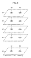
- Fig. 6 shows a configuration example of a substrate integral-type dislocation detection sensor, wherein a plurality of coils 62 have printed wiring in narrow width space, as the dislocation detection sensor on the substrate 61, and a integral-type substrate 63 is configured by laminating, for example, four layers of this substrate 61 having printed wiring.
- a integral-type substrate 63 space of the coils 62 can be narrowed.
- a compact-type detection coil with good precision can be obtained, and it can be built-in compactly, having high detection precision.
- magnetic field change by the coil as the dislocation detection sensor, however, for example, a permanent magnet or the like may be used so as to make ON/OFF mechanically.
- a magnetic field detection sensor such as an NR element (a magnetic resistance element), an MI element (a magnetic impedance element), a hole element.
- Fig. 7 shows a plan view showing arrangement relation among the detection rollers 34a --- and the dislocation detection sensors 33a ---, arranged in a staggered state.
- a detection unit 71 which is configured by providing, the 6 standard rollers 36-(refer to Fig. 3 ), the 6 detection rollers 34a to 34f, and the 12 dislocation detection sensors 33a to 331 having printed wiring onto the integral-type substrate 63, is located in two rows at the front stage side and the rear stage side in a carrying direction of the bill.
- the detection roller 34a at the rear stage side takes a configuration to be arranged, in a staggered state in a plan view, so as to correspond to the carrying space 72, as non-detection position between the detection rollers at the front stage side.
- Oscillation circuits 40a and 40b are provided as an alternate current magnetic field generation unit, and perform LC oscillation in the dislocation detection sensors 33a and 33b and the condensers 41a and 41b, and transistors 42a and 42b are used as negative resistances. After that, in detection circuits 43a and 43b, dislocation output from the oscillation circuits 40a and 40b is detected primarily to extract a dislocation component.
- Said oscillation circuits 40a and 40b are self-excited-type oscillation circuits for detecting dislocation amount of the roller, where the detection roller displaced elastically, based on variation of the alternate current magnetic field, when the alternate current magnetic field was generated. Therefore, it becomes possible to correct dispersion of the magnetic field of each channel, caused by dispersion of the coils or the condensers, by each channel, and thus to ensure a thickness sensor with good precision.
- Offset correction circuits 44a and 44b are circuits, as an adjustment unit for correcting dispersion of temperature variation or mechanical variation, and usually such subtraction correction circuits as to maintain a sensor level, not having the bill 30 before transaction, at a constant level.
- the sensor level is subjected to AD conversion sequentially at the timing of a switching control signal 48 by an AD converter 47, and a digital signal of the dislocation output is output to the control part 28 by the sensor processing part 35. Output thereof is input to a judgment part 49 in the control part 28, to judge number of the bill 30 or presence or absence of an adhered substance such as a tape.
- dislocation output it is converted to dislocation amount of the bill by inclination determined from a linear approximation equation of the thickness memorized by a nonvolatile memory 45, to calculate dislocation amount of each bill 30.
- this nonvolatile memory 45 there has been memorized, as a memory unit, inclinations of a linear approximation equation of dislocation of each channel a and b, calculated, in advance, from a plurality of dislocation levels. Still more, it has memorized output levels corresponding to two or more roller dislocation amounts relating to roller dislocation amount of the thickness of the bill, including an absent state of the bill, in advance. In this way, judgment processing at the control part 28 is made easy.
- output of the dislocation is input to the judgment part 49 in the control part 28, to judge number of the bill 30 or presence or absence of an adhered substance such as a tape.
- This control part 28 acts as a difference unit for determining difference between the input level of the dislocation detection sensors 33a --- in passing time of the bill, and the input level in non-passing time of the bill, adjusted by the offset correction circuits 44a and 44b, to judge thickness of the bill, by comparing the output level derived therefrom with the output level memorized by the nonvolatile memory 45. In this comparison judgment, by performing linear approximation between each of the thickness points, thickness dislocation amount can be determined correctly.
- the switching control signal 48 outputs a sampling timing signal synchronized with an encoder 27 (refer to Fig. 2 ), as well as outputs a switching timing signal to oscillation control circuits 50a and 50b. That is, the switching control signal 48 switches the channels a an b (refer to Fig. 5 ) by the non-adjacent group for acquiring the roller dislocation amount within unit detection time for detecting thickness in a carrying direction of thereof, by synchronizing with carrying speed of the bill 30 by the bill carrying mechanism.
- timing of data loading it is preferably configured by mechanism to output a pulse for travelling distance of the bill 30 by the encoder 27 or the like.
- passing speed of the bill 30 it may be configured by mechanism to output a signal synchronized with assumed passing speed of the bill.
- the oscillation control circuits 50a and 50 b output the switching control signal 48, during an ON period thereof, to the transistors 42a and 42b of negative resistances of the oscillation circuits 40a and 40b, and perform high frequency oscillation by making the transistors 42a and 42b thereof conducted.
- the oscillation circuits 40a and 40b perform high frequency oscillation only during a period when the oscillation control circuits 50a and 50 b are ON. Therefore, each of the oscillation control circuits 50a and 50b of the adjacent dislocation detection sensors 33a and 33b at the both sides is made ON at one side and OFF at the other side simultaneously, and thus are acting exclusively.
- the sensor processing part 35 acts as a processing unit, on the premise that detection level before switching is maintained, while a non-detection state switched to other non-adjacent group, and output data processed here is transferred to the control part 28.
- the control part 28 can be processed as usual.
- output data transferred to the control part 28 is handled as continued data, where detection level before switching is maintained, a ruggedness dislocation image with high resolution can be obtained.
- the twelve channels 33a to 331 are classified to two groups, that is a group having odd number 33a, 33c, --, and a group having even number 33b, 33d, -- (channels a and b), however, any grouping may be allowed as long as it is a channel configuration where adjacent dislocation detection sensors do not output simultaneously, that is, not to interfere each other.
- the dislocation detection sensors separated apart space between the dislocation detection sensors by two or three spaces may be handled as one group.
- Fig. 9B shows a waveform 52 representing the sum of dislocation outputs of each channel described in Fig. 9A .
- the judgment part 49 extracts a region where the bill 30 is contacting onto the detection rollers 34a, ---.
- the judgment part 49 extracts a region where the bill 30 is contacting onto the detection rollers 34a, ---.
- the judgment part 49 extracts a region where the bill 30 is contacting onto the detection rollers 34a, ---.
- the judgment part 49 extracts a region where the bill 30 is contacting onto the detection rollers 34a, ---.
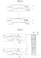
- Fig. 10 shows a waveform 55 of the dislocation detection sensors 33a and 33b among each of the channels a and b, in the case where an altered note adhered with the tape passes (refer to Fig. 4 ).
- the vertical axis shows dislocation output, and the horizontal axis shows travelling distance of the bill 30.
- a threshold value of these waveforms 55 because thickness of the bill 30 differs depending on places, or total thickness of the bill varies depending on environmental change of the bill itself, it is difficult to set the threshold value as it is. Therefore, firstly, a region is extracted where whole of the bill is mounted onto the roller.
- a region is extracted where whole of the bill is mounted onto the roller.
- one shown in Fig. 11 is a waveform 56 of the dislocation output, based on center value of total thickness of the bill (center of thickness in a carrying direction and a carrying width direction).
- an image 58 obtained by binary processing at the threshold value 57 of the convex part of each part of the bill from thickness of the bill of an object region, is shown, as a plan view of the bill.
- the area size thereof is equal to or larger than the threshold value 59, it is judged to have an adhered substance with a certain size, such as a tape. Therefore it can be detected in high precision, whether the bill 30 is carried in two or three sheets in an overlapped state, and whether it is an altered bill by a tape, paper or the like.
- the present invention should not be limited to configurations described in one Examples described above, and is applicable based on technological concept described in the appended claims.
- the bill 30 was used as one example of the medium, in one Examples described above, the present invention is applicable even to other media such as a slip, a check, a securities credit, a gold certificate and the like.
- the present invention is applicable to automatic transaction facilities such as automatic telling machines, exit fare machines, ticket-vending machines and the like, which handle bills or the like.
Landscapes
- Physics & Mathematics (AREA)
- General Physics & Mathematics (AREA)
- Inspection Of Paper Currency And Valuable Securities (AREA)
- Controlling Sheets Or Webs (AREA)
- Delivering By Means Of Belts And Rollers (AREA)
Abstract
Description
- The present invention relates to a medium thickness detection apparatus which detects thickness of media such as bills, securities, postage stamps which are utilized in transaction with automatic transaction facilities.
- In general, in a bill handling apparatus configured inside the automatic transaction facilities which are installed at an automatic transaction corner of financial institutions and the like, discernment of a deteriorated state of circulating notes or counterfeit bill is important, and thus a bill validator is provided inside the bill handling apparatus.
- In recent years, counterfeiting or altering technology of bills has become subtle, and altered notes are circulating, where various media such as bills, securities, postage stamps (hereafter referred to as leaves) are juggled with a micro tape, paper, seal or the like, which has thus required to correctly detect thickness characteristics of these altered notes to discern. For this purpose, it was required to enhance detection precision of the thickness detection apparatus. As one example thereof, there has been proposed a thickness detection apparatus for the leaves, for discerning whether the leaves are counterfeited or not, by thickness of the leaves (for example, refer to
JP-A-2006-4206 - Detection technology disclosed in the thickness detection apparatus of the leaves is one where a protuberance adhered with a tape or the like is detected by elastic dislocation of a detection roller, and amount of this dislocation is detected by a dislocation detection sensor, so as to detect that a tape or the like is adhered, by installing in an opposing way standard rollers, and detection rollers which elastically dislocate in response to thickness of the leaves, and by sandwiching and carrying the leaves sheet by sheet between these rollers.
- However, the above-described detection technology requires correct detection of all of a wide detection range of a paper surface. To attain this, it is necessary to align layout closely so as to eliminate clearance among said dislocation detection sensors by narrowing an arrangement space of the dislocation detection sensors, which are arranged in multiple in a carrying width direction, so as to eliminate a non-detection region of the leaves as less as possible, and.
- In the case where the arrangement space of the dislocation detection sensors was made narrow, however, interference of a magnetic field of adjacent dislocation detection sensors themselves is induced, and the interference becomes the more stringent with the closer arrangement, resulting in inhibiting correct measurement. Accordingly, limitation is generated in making the arrangement space of the dislocation detection sensors close, and at present it is necessary to take a certain space apart in the arrangement space of the dislocation detection sensors, and thus it was impossible to increase precision of thickness detection of the leaves. Therefore, in the case where, for example, folded bills or damaged circulating notes such as cut bills were carried in, there was a problem that it was impossible to count number thereof correctly.
- Accordingly, it is an object of the present invention to solve the problem and provide a medium thickness detection apparatus which is capable of detecting thickness of the media correctly, without interference of the magnetic field of the adjacent dislocation detection sensors, even by closely arranging a plurality of the dislocation detection sensors.
- The present invention is characterized by configured by comprising; standard rollers; a detection roller group for having an elastic member built-in, allowing elastic deformation in a radius direction, as well as arranging a plurality of detection rollers in the same axis direction opposing to the standard rollers; a carrying unit for sandwiching and carrying a medium between both rollers, by rotation driving at least one side of said opposing standard rollers and the detection roller group; and/or a dislocation detection sensor group for detecting dislocation amount of the roller where said detection rollers displaced elastically, by installing in an opposing way the dislocation detection sensors by each of said detection rollers, and/or based on variation of a magnetic field, which is generated from a coil of each of said dislocation detection rollers installed in an opposing way, wherein it is configured by comprising: a switching unit for dividing a plurality of the dislocation detection sensors, aligned along an axis direction of said detection rollers, to non-adjacent groups which are classified by each of non-adjacent groups themselves which are not adjacent in said alignment direction, and/or switching said non-adjacent groups for acquiring said roller dislocation amount.
- According to the present invention, it becomes possible to avoid interference of the magnetic field among the adjacent dislocation detection sensors, and thus, even by closely arranging the adjacent dislocation detection sensors, detection precision in high resolution can be obtained stably.
-
-
Fig. 1 is a configuration drawing of the inside of a bill carrying apparatus. -
Fig. 2 is a configuration drawing of the inside of a discerning part. -
Fig. 3 is a front elevation view showing arrangement relation among detection rollers and dislocation detection sensors. -
Fig. 4 is a front elevation view showing major parts of an example of a dislocation state of detection rollers. -
Figs. 5A and 5B are drawings explaining a switched state of each channel by a non-adjacent group of dislocation detection sensors. -
Fig. 6 is a perspective view showing a partial development of a substrate-integral-type dislocation detection sensor. -
Fig. 7 is a plan view showing arrangement relation among detection rollers and dislocation detection sensors, arranged in a staggered state. -
Fig. 8 is a block diagram of a control circuit of a thickness detection apparatus. -
Fig. 9A is a time chart showing detection data in each channel in judging the number of bills, andFig. 9B is a time chart showing a detection data to perform judgment of the sheet number of bills, by sum of each channel. -
Fig. 10 is a time chart showing a detection data in detecting altered notes. -
Fig. 11 is a drawing explaining a specific judgment state in detecting altered notes. - Explanation will be given below on embodiments of the present invention, with reference to drawings. The drawings show, for example, an automatic telling machine (ATM) installed at financial institutions such as banks, and show embodiments with enhanced detection performance of thickness at the discerning part which is built-in said ATM.
-
Fig. 1 shows a bill carrying apparatus configured inside the ATM, which is one Example of the present invention, and explanation will be given in this Example on the case where bills were processed as an example of a medium. - In this bill carrying apparatus, 1 represents a temporal stock part for temporarily accumulating bills counted; 2 represents a discerning part for discerning money types, authenticity, orientation, and degree of damage of bills; 3a to 3d represent storage parts for accumulating bills by type; 4 represents a recovery part for storing the bills rejected by the
discerning part 2; 5 represents an upper carrying route for carrying bills by looping amoney entrance port 20, thediscerning part 2, the temporal stock part 1, amoney exit port 21 having a shutter, and a return port 22; 6 represents a lower carrying route for carrying bills from the upper carrying route 5 and via the upper part of thestorage parts 3a to 3d and therecovery part 4, and again to the upper carrying route 5; 7 represents a money entrance port carrying route for carrying bills from themoney entrance port 20 to the upper carrying route 5; 8 represents a money exit port carrying route for carrying bills from the upper carrying route 5 to themoney exit port 21 having a shutter; 9 represents a return port carrying route for carrying bills from the upper carrying route 5 to the return port 22; 10 represents a temporal stock part storing and carrying route for carrying bills from the upper carrying route 5 to the temporal stock part 1; 11 represents a temporal stock part sending-out and carrying route for carrying bills from the temporal stock part 1 to the upper carrying route 5; 12a to 12d represent an storage part storing and carrying route for carrying bills from the lower carryingroute 6 to thestorage parts 3a to 3d; 13a to 13d represent an storage part sending-out and carrying route for carrying bills from thestorage parts 3a to 3d to the lower carryingroute 6; 14 represents a recovery part carrying route for carrying bills from the lower carryingroute 6 to therecovery part 4; 15 represents a passing-through sensor for detecting passing-through of bills; 16 represents a gate for switching a direction for carrying bills; 17 represents a money entrance port bill detection sensor for detecting whether bills are present or not at themoney entrance port 20; 18 represents a money exit port bill detection sensor for detecting whether bills are present or not at themoney exit port -
Fig. 2 is an outline drawing showing a major configuration of thediscerning part 2. - This
discerning part 2 is provided with abill carrying mechanism 31 for discerning while carryingbills 30 introduced thereto. Thisbill carrying mechanism 31 is installed with acarrying roller part 23 provided with an uppercarrying roller 23a and a lower carrying roller 23b erected in an opposing way up and down, at carrying route width. These upper andlower carrying rollers 23a and 23b rotate by rotation force transferred from a carrying motor not shown, and thebill 30 is introduced here in a horizontally long state, and carry sheet by sheet by sandwiching saidbill 30 from upper and lower directions. In addition, they have a configuration with high carrying tolerance enabling overlapped carrying, so that smooth carrying is possible even for damaged circulating notes such as folded bills or cut bills. - In addition, in the
discerning part 2, there are provided, subsequent to thecarrying roller part 23, a color linear sensor 24 for checking penetration amount of thebill 30 and penetration amount of ink; a magnetic sensor 25 for discerning magnetic properties of magnetic ink coated on thebill 30; a thickness sensor 26 for detecting thickness of thebill 30, presence or absence of a tape and ruggedness of a thread or the like; anencoder 27 for outputting a clock signal in synchronizing with a carrying distance of thebill 30, based on carrying drive at thebill carrying mechanism 31, and acontrol part 28 for judging money types, number, and authenticity from a detected data of the thickness sensor 26. - Accordingly, the
discerning part 2 discerns to which money type thebill 30 belongs, which was introduced thereto, still more discerns whether it is a true note or a counterfeited note, and still more discerns whether thebill 30 is one sheet or two sheets or three or more sheets, so as to manage thebill 30 to be utilized in transaction. It should be noted that thebill carrying mechanism 31 is configured to make discernment possible, even when thebill 30 is carried from either of the reciprocating directions. - Explanation will be given next on a specific configuration of the thickness sensor 26 provided to the
discerning part 2, with reference toFig. 3 . - This thickness sensor 26 is provided with a
standard roller axis 37 as a rotating axis where rotation force is transmitted from a carrying drive system of thebill carrying mechanism 31;standard rollers 36 arranged, for example, in 6 sheets, in a narrow width space in the same axis direction as thisstandard roller axis 37; sixdetection rollers 34a to 34f arranged on adetection roller axis 38 opposing to said sixstandard rollers 36; adetection roller group 34 which is driven-rotated when these 6detection rollers 34a to 34f are pressed to thestandard rollers 36;dislocation detection sensors 33a to 331, in a total number of 12, arranged in an opposing way, for example, by each 2 sensors, every thedetection rollers 34a to 34f; a dislocationdetection sensor group 33 for detecting roller dislocation amount where thedetection rollers 34a to 34f displaced elastically, based on variation of a magnetic field, which is generated from a coil of each of thedislocation detection sensors 33a to 331, and asensor processing part 35 for processing input data from said dislocationdetection sensor group 33. Thestandard rollers 36 were shown for the case of arraying 6 rollers in a carrying width direction, however, they may be configured by one long roller axis. -
Fig. 4 is a drawing explaining a major part by magnifying a part of the thickness sensor 26. Here explanation will be given on two sets of a left detection part composed of twodislocation detection sensors detection rollers 34a, and thestandard rollers 36 in an upper and lower direction; and a right detection part composed of twodislocation detection sensors detection roller 34b and thestandard rollers 36 in an upper and lower direction at the right side thereof, as an example, in view of explaining this thickness sensor 26. - The
detection rollers elastic members 39a, 39b, ---, such as rubber, between anexternal wheel 32a, which is composed of a cylinder-like member of a metal or the like, and thedetection roller axis 38, which becomes a center axis thereof. On the other hand, thestandard roller 36 is configured by a metal and provided as a standard surface without dislocation of the exterior circumference surface, to which thedetection rollers - By this, when the
bill 30 is meshed between the surfaces of the two set of rollers, that is, thestandard rollers detection rollers elastic members 39a and 39b deform by thickness amount of thebill 30, and theexternal wheels 32a and 32b displace in the upper direction. - This dislocation amount is detected by the two
dislocation detection sensors dislocation detection sensors bill 30 is output. The detection signal is processed at thesensor processing part 35, and a digital signal for the dislocation amount thereof is sent to thecontrol part 28. In thecontrol part 28, it is judged whether thebill 30 is carried or not in two or more sheets in an overlapped state, whether it is a altered note adhered with a tape or the like or not, or whether it is a true note or a counterfeited note or not, based on thickness data of thebill 30 sent. - In addition, by arranging two
dislocation detection sensors detection roller 34a, in the case where, for example, a tape TA is adhered at the paper surface (refer toFig. 4 ), both ends of said tape TA contact over thedetection rollers detection rollers detection rollers - In order to detect a wide detection range of the
bill 30 correctly, it is preferable that layout of a plurality of thedislocation detection sensors 33a to 331 has narrow arrangement space and eliminates clearance among said sensors, so as to decrease a non-detection region of thebill 30 as low as possible. Therefore, each of thedislocation detection sensors 33a to 331, which are aligned over a carrying width direction, is arranged closely by narrowing arrangement space. - Therefore, these
dislocation detection sensors 33a to 331 are arranged in such close vicinity as having little clearance and resulting in interference of mutual magnetic field by adjacent dislocation detection sensors themselves. Explanation will be given next on thickness detection technology which is capable of detecting thickness of thebill 30 correctly, without interference of the magnetic field of the adjacentdislocation detection sensors 33a to 331, even by closely arranging the space of thedislocation detection sensors 33a to 331. - This thickness detection technology is such technology to divide a plurality of the
dislocation detection sensors 33a to 331 aligned along an axis direction of thedetection rollers 34a to 34f, to two channels (channels a and b inFig. 5 ) of two non-adjacent groups which are classified by each of non-adjacent groups themselves which are not adjacent in said alignment direction, and alternately switching (ON/OFF) the power of an oscillation voltage to thus divided non-adjacent groups, as shown inFig. 5A . - For example, as shown in
Fig. 5B , thedislocation detection sensors 33a to 33d are classified to two groups, that is a group havingodd number number odd number group even number group - It aims at avoiding simultaneous output (interference) of the adjacent dislocation detection sensors, in controlling oscillation of these two kinds of groups, in the case where each of the dislocation detection sensors outputs (oscillates). That is, this grouping contributes as a means for avoiding interference.
- In this way, a magnetic field is generated by oscillating a predetermined frequency by a coil of the dislocation detection sensor, however, because of alternate oscillation by the two kinds of groups separated apart by one space, without simultaneous oscillation from these
dislocation detection sensors 33a to 33d, there is no influence of the magnetic field from the adjacent dislocation detection sensors, even when said dislocation detection sensors are arranged closely. - In this way, it becomes possible to avoid interference of the magnetic field between the dislocation detection sensors, and obtain detection precision in high resolution stably, even when the dislocation detection sensors are arranged closely.
-
Fig. 6 shows a configuration example of a substrate integral-type dislocation detection sensor, wherein a plurality ofcoils 62 have printed wiring in narrow width space, as the dislocation detection sensor on thesubstrate 61, and a integral-type substrate 63 is configured by laminating, for example, four layers of thissubstrate 61 having printed wiring. By using this integral-type substrate 63, space of thecoils 62 can be narrowed. As a result, a compact-type detection coil with good precision can be obtained, and it can be built-in compactly, having high detection precision. - It should be noted that explanation was given on magnetic field change by the coil as the dislocation detection sensor, however, for example, a permanent magnet or the like may be used so as to make ON/OFF mechanically. In addition, there may be used a magnetic field detection sensor such as an NR element (a magnetic resistance element), an MI element (a magnetic impedance element), a hole element.
- It should be noted that, the explanation was given in the explanation on unique detection technology for avoiding influence of the magnetic field, however, it is also possible to increase detection precision still more. That is, in the case of the arrangement configuration of the
dislocation detection sensors 33a to 331, adjacent space of thedetection rollers bill 30, and thus generates a carryingspace 72 of the non-detected place (refer toFig. 7 ). To solve this, one example of a configuration will be shown next, which is capable of providing supplemental detection even for said carryingspace 72. -
Fig. 7 shows a plan view showing arrangement relation among thedetection rollers 34a --- and thedislocation detection sensors 33a ---, arranged in a staggered state. For example, adetection unit 71, which is configured by providing, the 6 standard rollers 36-(refer toFig. 3 ), the 6detection rollers 34a to 34f, and the 12dislocation detection sensors 33a to 331 having printed wiring onto the integral-type substrate 63, is located in two rows at the front stage side and the rear stage side in a carrying direction of the bill. Among these, thedetection roller 34a at the rear stage side takes a configuration to be arranged, in a staggered state in a plan view, so as to correspond to the carryingspace 72, as non-detection position between the detection rollers at the front stage side. - By this configuration, although the carrying
space 72 is generated inevitably between a plurality of thedetection rollers 34a an 34b, because detection of all surfaces of thebill 30 is possible without missing, by supplemental detection by thedetection roller 34a at the later stage side, even for this carryingspace 72, ruggedness dislocation of the bill can be detected correctly, even when detection range of the paper surface is wide. - Explanation will be given next on a control configuration of the thickness sensor 26, with reference to
Fig. 8 . Here, explanation will be given below on the case of controlling twodislocation detection sensors -
Oscillation circuits dislocation detection sensors condensers 41a and 41b, andtransistors 42a and 42b are used as negative resistances. After that, indetection circuits oscillation circuits - Said
oscillation circuits - Offset
correction circuits 44a and 44b are circuits, as an adjustment unit for correcting dispersion of temperature variation or mechanical variation, and usually such subtraction correction circuits as to maintain a sensor level, not having thebill 30 before transaction, at a constant level. In amultiplexer circuit 46, the sensor level is subjected to AD conversion sequentially at the timing of a switchingcontrol signal 48 by anAD converter 47, and a digital signal of the dislocation output is output to thecontrol part 28 by thesensor processing part 35. Output thereof is input to ajudgment part 49 in thecontrol part 28, to judge number of thebill 30 or presence or absence of an adhered substance such as a tape. - In addition, in judging the dislocation output, it is converted to dislocation amount of the bill by inclination determined from a linear approximation equation of the thickness memorized by a
nonvolatile memory 45, to calculate dislocation amount of eachbill 30. In thisnonvolatile memory 45, there has been memorized, as a memory unit, inclinations of a linear approximation equation of dislocation of each channel a and b, calculated, in advance, from a plurality of dislocation levels. Still more, it has memorized output levels corresponding to two or more roller dislocation amounts relating to roller dislocation amount of the thickness of the bill, including an absent state of the bill, in advance. In this way, judgment processing at thecontrol part 28 is made easy. - After that, output of the dislocation is input to the
judgment part 49 in thecontrol part 28, to judge number of thebill 30 or presence or absence of an adhered substance such as a tape. Thiscontrol part 28 acts as a difference unit for determining difference between the input level of thedislocation detection sensors 33a --- in passing time of the bill, and the input level in non-passing time of the bill, adjusted by the offsetcorrection circuits 44a and 44b, to judge thickness of the bill, by comparing the output level derived therefrom with the output level memorized by thenonvolatile memory 45. In this comparison judgment, by performing linear approximation between each of the thickness points, thickness dislocation amount can be determined correctly. - In this way, it becomes possible to determine thickness dislocation amount without influence of dispersion of sensor temperature or the apparatus, as well as secure linearity between thickness dislocation amounts memorized by the
nonvolatile memory 45, and thus a thickness sensor with high dynamic range can be prepared. Therefore, it becomes possible to secure a thickness sensor with good precision. - The switching
control signal 48 outputs a sampling timing signal synchronized with an encoder 27 (refer toFig. 2 ), as well as outputs a switching timing signal tooscillation control circuits control signal 48 switches the channels a an b (refer toFig. 5 ) by the non-adjacent group for acquiring the roller dislocation amount within unit detection time for detecting thickness in a carrying direction of thereof, by synchronizing with carrying speed of thebill 30 by the bill carrying mechanism. - In this way, a ruggedness dislocation image without resolution change for a carrying direction can be obtained, even when carrying speed varies. It should be noted that, as for timing of data loading, it is preferably configured by mechanism to output a pulse for travelling distance of the
bill 30 by theencoder 27 or the like. In the case where passing speed of thebill 30 is known in advance, it may be configured by mechanism to output a signal synchronized with assumed passing speed of the bill. - The
oscillation control circuits control signal 48, during an ON period thereof, to thetransistors 42a and 42b of negative resistances of theoscillation circuits transistors 42a and 42b thereof conducted. Theoscillation circuits oscillation control circuits oscillation control circuits dislocation detection sensors - In the case of data transfer from the
sensor processing part 35 to thecontrol part 28 of a high rank control section, thesensor processing part 35 acts as a processing unit, on the premise that detection level before switching is maintained, while a non-detection state switched to other non-adjacent group, and output data processed here is transferred to thecontrol part 28. In this way, thecontrol part 28 can be processed as usual. In particular, because output data transferred to thecontrol part 28 is handled as continued data, where detection level before switching is maintained, a ruggedness dislocation image with high resolution can be obtained. - In the above-described example, the twelve
channels 33a to 331 are classified to two groups, that is a group havingodd number even number - Explanation will be given next on a method for judging how many sheets of the
bill 30 are carried in thejudgment part 49, with reference toFig. 9 . In awaveform 51 represented inFig. 9A , the vertical axis shows dislocation output of each channel CH0, CH1-CH10, CH11 (a, b), and the horizontal axis shows travelling distance of thebill 30. -
Fig. 9B shows awaveform 52 representing the sum of dislocation outputs of each channel described inFig. 9A . - Firstly, the
judgment part 49 extracts a region where thebill 30 is contacting onto thedetection rollers 34a, ---. In this case, when average value of thebill 30 is equal to or more thanthreshold value 53 corresponding to 2.5 sheets of thebill 30, it is judged to be equal to or more than 3 sheets; and as for the sheets below that, when it is equal to or more thanthreshold value 54 corresponding to 1.5 sheets of thebill 30, it is judged to be 2 sheets; and when it is belowthreshold value 54, it t is judged to be 1 sheet. - Explanation will be given next on a judgment method for a tape adhered to the
bill 30 in thejudgment part 49, with reference toFig. 10 and Fig. 11 . -
Fig. 10 shows awaveform 55 of thedislocation detection sensors Fig. 4 ). The vertical axis shows dislocation output, and the horizontal axis shows travelling distance of thebill 30. - As for a threshold value of these
waveforms 55, because thickness of thebill 30 differs depending on places, or total thickness of the bill varies depending on environmental change of the bill itself, it is difficult to set the threshold value as it is. Therefore, firstly, a region is extracted where whole of the bill is mounted onto the roller. In this case, one shown inFig. 11 is awaveform 56 of the dislocation output, based on center value of total thickness of the bill (center of thickness in a carrying direction and a carrying width direction). And, animage 58, obtained by binary processing at the threshold value 57 of the convex part of each part of the bill from thickness of the bill of an object region, is shown, as a plan view of the bill. And, when the area size thereof is equal to or larger than the threshold value 59, it is judged to have an adhered substance with a certain size, such as a tape. Therefore it can be detected in high precision, whether thebill 30 is carried in two or three sheets in an overlapped state, and whether it is an altered bill by a tape, paper or the like. - As described above, since it is possible to avoid interference of the magnetic field among the adjacent dislocation detection sensors, even by closely arranging said adjacent dislocation detection sensors, detection precision in high resolution can be obtained stably. Therefore, it becomes possible to detect, by correct judgment, a fine ruggedness variation state of a medium, irrespective of a carrying state of the medium, and thus judgment in high precision satisfying security function of the bill can be performed,.
- The present invention should not be limited to configurations described in one Examples described above, and is applicable based on technological concept described in the appended claims. For example, although the
bill 30 was used as one example of the medium, in one Examples described above, the present invention is applicable even to other media such as a slip, a check, a securities credit, a gold certificate and the like. - The present invention is applicable to automatic transaction facilities such as automatic telling machines, exit fare machines, ticket-vending machines and the like, which handle bills or the like.
- Features, components and specific details of the structures of the above-described embodiments may be exchanged or combined to form further embodiments optimized for the respective application. As far as those modifications are apparent for an expert skilled in the art they shall be disclosed implicitly by the above description without specifying explicitly every possible combination.
Claims (7)
- A medium thickness detection apparatus configured by comprising:standard rollers (36);
a detection roller group (34) for having an elastic member (39) built-in, allowing elastic deformation in a radius direction, as well as arranging a plurality of detection rollers (34a to 34f) in the same axis direction opposing to the standard rollers (36);
a carrying unit for sandwiching and carrying a medium between both rollers, by rotation driving at least one side of said opposing standard rollers (36) and the detection roller group (34); and
a dislocation detection sensor group (33) for detecting dislocation amount of the roller where said detection rollers (34a to 34f) displaced elastically, by installing in an opposing way the dislocation detection sensors (33a to 331) by each of said detection rollers (34a to 34f), and based on variation of a magnetic field, which is generated from a coil (62) of each of said dislocation detection sensors (33a to 331) installed in an opposing way,
wherein it is configured by comprising:a switching unit for dividing a plurality of the dislocation detection sensors (33a to 331), aligned along an axis direction of said detection rollers (34a to 34f), to non-adjacent groups which are classified by each of non-adjacent groups themselves which are not adjacent in said alignment direction, and switching said non-adjacent groups for acquiring said roller dislocation amount. - The medium thickness detection apparatus according to claim 1, having a configuration located a plurality of the medium thickness detection units, which are configured by comprising said standard rollers (36), said detection roller group (34) and said dislocation detection sensor group (33), in a medium carrying direction; and
arranged in a staggered state, at least the detection rollers (34a to 34f) of the medium thickness detection units, which is located at the front stage side and the rear stage side in said medium carrying direction, so that, at a non-detection position between the detection rollers (34a to 34f) at one side, the detection rollers (34a to 34f) at the other side are arranged in an opposing way at the front stage side and the rear stage side. - The medium thickness detection apparatus according to claim 1 or 2, wherein said switching unit has a configuration for switching said non-adjacent group for acquiring said roller dislocation amount within unit detection time for detecting thickness in a carrying direction of the medium, by synchronizing with carrying speed of the medium by said carrying unit.
- The medium thickness detection apparatus according to claim 1, 2 or 3, comprising:an adjustment unit for adjusting an input level of the dislocation detection sensor (33), in non-passing time of the medium, to a predetermined level;a memory unit for memorizing, in advance, an output level corresponding to dislocation amount of at least two or more rollers, relating to roller dislocation amount of medium thickness ;a difference unit for determining difference between the input level of the dislocation detection sensors (33a to 331) in passing time of the medium, and the predetermined level in non-passing time of the medium, adjusted by said adjustment unit; anda judgment unit for judging thickness of the medium, by comparing the output level determined by said difference unit, and the output level which said memory unit has memorized.
- The medium thickness detection apparatus according to any one of claims 1 to 4, comprising:a memory unit for temporarily memorizing data which said dislocation detection sensor (33) detected;a processing unit for processing data on the premise that detection level before switching is maintained during a non-detection state switched to other non-adjacent group;a transfer unit for transferring data of the roller dislocation amount to a higher rank control section; anda control unit for transferring, by said transfer unit, the output data processed by said processing unit.
- The medium thickness detection apparatus according to any one of claims 1 to 5, wherein a plurality of said dislocation detection sensors (33a to 331) are configured by a coil (62) having printed wiring at a substrate.
- The medium thickness detection apparatus according to any one of claims 1 to 6, wherein said dislocation detection sensors (33a to 331) are configured by:an alternate current magnetic field generation unit for generating the alternate current magnetic field; anda self-excited-type oscillation circuit for detecting dislocation amount of the roller, where the detection rollers (34a to 34f) displaced elastically, based on variation of the alternate current magnetic field, which was generated by said alternate current magnetic field generation unit.
Applications Claiming Priority (1)
| Application Number | Priority Date | Filing Date | Title |
|---|---|---|---|
| JP2009107633A JP2010257292A (en) | 2009-04-27 | 2009-04-27 | Medium thickness detector |
Publications (2)
| Publication Number | Publication Date |
|---|---|
| EP2249315A1 true EP2249315A1 (en) | 2010-11-10 |
| EP2249315B1 EP2249315B1 (en) | 2014-11-19 |
Family
ID=42320837
Family Applications (1)
| Application Number | Title | Priority Date | Filing Date |
|---|---|---|---|
| EP10161039.2A Not-in-force EP2249315B1 (en) | 2009-04-27 | 2010-04-26 | Medium thickness detection apparatus |
Country Status (4)
| Country | Link |
|---|---|
| EP (1) | EP2249315B1 (en) |
| JP (1) | JP2010257292A (en) |
| KR (1) | KR101159961B1 (en) |
| CN (1) | CN101872501B (en) |
Cited By (2)
| Publication number | Priority date | Publication date | Assignee | Title |
|---|---|---|---|---|
| EP3236432A4 (en) * | 2014-12-15 | 2018-01-24 | Fujitsu Frontech Limited | Thickness detection device |
| US10008065B2 (en) | 2013-12-12 | 2018-06-26 | Grg Banking Equipment Co., Ltd. | Method and device for banknote identification based on thickness signal identification |
Families Citing this family (10)
| Publication number | Priority date | Publication date | Assignee | Title |
|---|---|---|---|---|
| JP5593247B2 (en) * | 2011-02-01 | 2014-09-17 | 日立オムロンターミナルソリューションズ株式会社 | Medium thickness detector |
| CN102722933B (en) * | 2012-06-11 | 2014-08-20 | 广州广电运通金融电子股份有限公司 | Device for detecting thickness of sheet medium and method thereof |
| JP5997018B2 (en) * | 2012-11-21 | 2016-09-21 | 日立オムロンターミナルソリューションズ株式会社 | Paper sheet thickness detection device and paper sheet identification device |
| CN103136840B (en) * | 2013-01-23 | 2014-12-31 | 广州广电运通金融电子股份有限公司 | Magnetic levitation type slice medium thickness detecting device |
| CN103617671B (en) * | 2013-12-12 | 2016-08-17 | 广州广电运通金融电子股份有限公司 | The recognition methods of a kind of thickness abnormity banknote and system |
| CN104077831B (en) * | 2014-07-18 | 2016-08-24 | 广州广电运通金融电子股份有限公司 | A kind of value document magnetic detection device |
| CN106898080B (en) * | 2017-03-22 | 2023-01-13 | 深圳怡化电脑股份有限公司 | Thickness detection device and financial equipment |
| CN106909086B (en) * | 2017-03-30 | 2019-06-07 | 深圳怡化电脑股份有限公司 | A kind of detection method and its device of abnormal data |
| CN107680243B (en) * | 2017-09-04 | 2019-11-05 | 东方通信股份有限公司 | Note thickness measurement device and measurement method based on infrared sensor transmission |
| CN112605133A (en) * | 2020-12-11 | 2021-04-06 | 杭州电子科技大学 | Rolled plate strip thickness detection device and control system |
Citations (3)
| Publication number | Priority date | Publication date | Assignee | Title |
|---|---|---|---|---|
| US20010035329A1 (en) * | 2000-03-16 | 2001-11-01 | Kinya Toda | Sheet counting apparatus, sheet counting method and transaction apparatus |
| JP2006004206A (en) | 2004-06-18 | 2006-01-05 | Hitachi Omron Terminal Solutions Corp | Paper sheet thickness detection device and bill handling device |
| US20060055105A1 (en) * | 2004-09-15 | 2006-03-16 | Ryota Kawaguchi | Thickness detecting apparatus |
Family Cites Families (10)
| Publication number | Priority date | Publication date | Assignee | Title |
|---|---|---|---|---|
| JPS60228901A (en) * | 1984-04-27 | 1985-11-14 | Toshiba Corp | Deflection detector for conductor |
| JP3768280B2 (en) * | 1996-01-30 | 2006-04-19 | グローリー工業株式会社 | Optical data collection device for paper |
| JP3642931B2 (en) * | 1997-09-25 | 2005-04-27 | 沖電気工業株式会社 | Paper sheet thickness detection apparatus and correction method thereof |
| CA2230523C (en) * | 1998-02-25 | 2006-05-09 | Cashcode Company Inc. | Induction sensor |
| WO2001036904A1 (en) * | 1999-11-18 | 2001-05-25 | Fujitsu Limited | Pachymeter |
| JP2002269615A (en) * | 2001-03-09 | 2002-09-20 | Canon Electronics Inc | Coin identification device |
| JP4031962B2 (en) * | 2002-08-26 | 2008-01-09 | 日立オムロンターミナルソリューションズ株式会社 | Paper thickness detector |
| JP4507585B2 (en) * | 2003-12-16 | 2010-07-21 | 日本電産サンキョー株式会社 | Drive circuit for paper sheet identification sensor and paper sheet identification device |
| CN200968853Y (en) * | 2006-11-10 | 2007-10-31 | 柳长庆 | Thickness measuring mechanism |
| KR101456707B1 (en) * | 2007-12-12 | 2014-10-31 | 주식회사 엘지씨엔에스 | Medium thickness detecting device |
-
2009
- 2009-04-27 JP JP2009107633A patent/JP2010257292A/en active Pending
-
2010
- 2010-04-26 EP EP10161039.2A patent/EP2249315B1/en not_active Not-in-force
- 2010-04-26 KR KR1020100038342A patent/KR101159961B1/en not_active Expired - Fee Related
- 2010-04-27 CN CN2010101689418A patent/CN101872501B/en not_active Expired - Fee Related
Patent Citations (4)
| Publication number | Priority date | Publication date | Assignee | Title |
|---|---|---|---|---|
| US20010035329A1 (en) * | 2000-03-16 | 2001-11-01 | Kinya Toda | Sheet counting apparatus, sheet counting method and transaction apparatus |
| JP2006004206A (en) | 2004-06-18 | 2006-01-05 | Hitachi Omron Terminal Solutions Corp | Paper sheet thickness detection device and bill handling device |
| EP1764751A1 (en) * | 2004-06-18 | 2007-03-21 | Hitachi-Omron Terminal Solutions, Corp. | Thickness detector for paper sheet and paper money handling device |
| US20060055105A1 (en) * | 2004-09-15 | 2006-03-16 | Ryota Kawaguchi | Thickness detecting apparatus |
Cited By (2)
| Publication number | Priority date | Publication date | Assignee | Title |
|---|---|---|---|---|
| US10008065B2 (en) | 2013-12-12 | 2018-06-26 | Grg Banking Equipment Co., Ltd. | Method and device for banknote identification based on thickness signal identification |
| EP3236432A4 (en) * | 2014-12-15 | 2018-01-24 | Fujitsu Frontech Limited | Thickness detection device |
Also Published As
| Publication number | Publication date |
|---|---|
| KR101159961B1 (en) | 2012-06-25 |
| EP2249315B1 (en) | 2014-11-19 |
| KR20100118075A (en) | 2010-11-04 |
| CN101872501A (en) | 2010-10-27 |
| CN101872501B (en) | 2012-08-22 |
| JP2010257292A (en) | 2010-11-11 |
Similar Documents
| Publication | Publication Date | Title |
|---|---|---|
| EP2249315B1 (en) | Medium thickness detection apparatus | |
| JP4444738B2 (en) | Paper thickness detector | |
| JP4366104B2 (en) | Paper sheet discrimination device | |
| CN101266701A (en) | Banknote identification device | |
| JP5603259B2 (en) | Paper sheet identification device | |
| US20150220936A1 (en) | Valuable document authentication method and device | |
| JP5395859B2 (en) | Paper sheet thickness detection device and bill handling device | |
| WO2012105113A1 (en) | Media-thickness detection device and automatic transaction machine | |
| KR20030025187A (en) | Apparatus of count for paper money and apparatus of process for dealing | |
| US9902582B2 (en) | Apparatus and method for controlling a banknote feed rate | |
| US20110273191A1 (en) | Device for determining a thickness or thickness variation of a flat object | |
| JP2010152611A (en) | Paper currency discrimination device | |
| JP3745372B2 (en) | Distributed processing device | |
| WO2013080485A1 (en) | Medium recognition device, banknote handling device, and medium recognition method | |
| KR100804134B1 (en) | Check character recognition method of check and withdrawal device | |
| KR101388049B1 (en) | Apparatus for magnetic ink character recognition and method for operating the same | |
| US10803691B2 (en) | Device for detecting a magnetic security feature of a value document and method for measured value compensation for the detection of a magnetic security feature of a value document | |
| JP4645428B2 (en) | Bill validator | |
| KR920005626B1 (en) | Paper currency deliverer | |
| JPS6170690A (en) | Discrimination of sheet paper | |
| JP5109353B2 (en) | Bill recognition device | |
| CN106067213A (en) | A kind of device for detecting thickness of medium and method | |
| JPH04217092A (en) | Device for discriminating true or fake of paper money | |
| JPS61202293A (en) | Banknote identification device | |
| WO2000013128A1 (en) | Improvements in and relating to sheet material inspection apparatus and methods |
Legal Events
| Date | Code | Title | Description |
|---|---|---|---|
| PUAI | Public reference made under article 153(3) epc to a published international application that has entered the european phase |
Free format text: ORIGINAL CODE: 0009012 |
|
| 17P | Request for examination filed |
Effective date: 20100917 |
|
| AK | Designated contracting states |
Kind code of ref document: A1 Designated state(s): AT BE BG CH CY CZ DE DK EE ES FI FR GB GR HR HU IE IS IT LI LT LU LV MC MK MT NL NO PL PT RO SE SI SK SM TR |
|
| AX | Request for extension of the european patent |
Extension state: AL BA ME RS |
|
| GRAP | Despatch of communication of intention to grant a patent |
Free format text: ORIGINAL CODE: EPIDOSNIGR1 |
|
| RIC1 | Information provided on ipc code assigned before grant |
Ipc: G07D 7/16 20060101AFI20140519BHEP |
|
| INTG | Intention to grant announced |
Effective date: 20140611 |
|
| RIN1 | Information on inventor provided before grant (corrected) |
Inventor name: MAI, JIAN ZHONG |
|
| GRAS | Grant fee paid |
Free format text: ORIGINAL CODE: EPIDOSNIGR3 |
|
| GRAA | (expected) grant |
Free format text: ORIGINAL CODE: 0009210 |
|
| AK | Designated contracting states |
Kind code of ref document: B1 Designated state(s): AT BE BG CH CY CZ DE DK EE ES FI FR GB GR HR HU IE IS IT LI LT LU LV MC MK MT NL NO PL PT RO SE SI SK SM TR |
|
| REG | Reference to a national code |
Ref country code: GB Ref legal event code: FG4D |
|
| REG | Reference to a national code |
Ref country code: CH Ref legal event code: EP |
|
| REG | Reference to a national code |
Ref country code: AT Ref legal event code: REF Ref document number: 697406 Country of ref document: AT Kind code of ref document: T Effective date: 20141215 |
|
| REG | Reference to a national code |
Ref country code: IE Ref legal event code: FG4D |
|
| REG | Reference to a national code |
Ref country code: DE Ref legal event code: R096 Ref document number: 602010020319 Country of ref document: DE Effective date: 20141231 |
|
| REG | Reference to a national code |
Ref country code: NL Ref legal event code: VDEP Effective date: 20141119 |
|
| REG | Reference to a national code |
Ref country code: AT Ref legal event code: MK05 Ref document number: 697406 Country of ref document: AT Kind code of ref document: T Effective date: 20141119 |
|
| REG | Reference to a national code |
Ref country code: LT Ref legal event code: MG4D |
|
| PG25 | Lapsed in a contracting state [announced via postgrant information from national office to epo] |
Ref country code: NO Free format text: LAPSE BECAUSE OF FAILURE TO SUBMIT A TRANSLATION OF THE DESCRIPTION OR TO PAY THE FEE WITHIN THE PRESCRIBED TIME-LIMIT Effective date: 20150219 Ref country code: PT Free format text: LAPSE BECAUSE OF FAILURE TO SUBMIT A TRANSLATION OF THE DESCRIPTION OR TO PAY THE FEE WITHIN THE PRESCRIBED TIME-LIMIT Effective date: 20150319 Ref country code: NL Free format text: LAPSE BECAUSE OF FAILURE TO SUBMIT A TRANSLATION OF THE DESCRIPTION OR TO PAY THE FEE WITHIN THE PRESCRIBED TIME-LIMIT Effective date: 20141119 Ref country code: LT Free format text: LAPSE BECAUSE OF FAILURE TO SUBMIT A TRANSLATION OF THE DESCRIPTION OR TO PAY THE FEE WITHIN THE PRESCRIBED TIME-LIMIT Effective date: 20141119 Ref country code: IS Free format text: LAPSE BECAUSE OF FAILURE TO SUBMIT A TRANSLATION OF THE DESCRIPTION OR TO PAY THE FEE WITHIN THE PRESCRIBED TIME-LIMIT Effective date: 20150319 Ref country code: ES Free format text: LAPSE BECAUSE OF FAILURE TO SUBMIT A TRANSLATION OF THE DESCRIPTION OR TO PAY THE FEE WITHIN THE PRESCRIBED TIME-LIMIT Effective date: 20141119 Ref country code: FI Free format text: LAPSE BECAUSE OF FAILURE TO SUBMIT A TRANSLATION OF THE DESCRIPTION OR TO PAY THE FEE WITHIN THE PRESCRIBED TIME-LIMIT Effective date: 20141119 |
|
| PG25 | Lapsed in a contracting state [announced via postgrant information from national office to epo] |
Ref country code: PL Free format text: LAPSE BECAUSE OF FAILURE TO SUBMIT A TRANSLATION OF THE DESCRIPTION OR TO PAY THE FEE WITHIN THE PRESCRIBED TIME-LIMIT Effective date: 20141119 Ref country code: CY Free format text: LAPSE BECAUSE OF FAILURE TO SUBMIT A TRANSLATION OF THE DESCRIPTION OR TO PAY THE FEE WITHIN THE PRESCRIBED TIME-LIMIT Effective date: 20141119 Ref country code: AT Free format text: LAPSE BECAUSE OF FAILURE TO SUBMIT A TRANSLATION OF THE DESCRIPTION OR TO PAY THE FEE WITHIN THE PRESCRIBED TIME-LIMIT Effective date: 20141119 Ref country code: HR Free format text: LAPSE BECAUSE OF FAILURE TO SUBMIT A TRANSLATION OF THE DESCRIPTION OR TO PAY THE FEE WITHIN THE PRESCRIBED TIME-LIMIT Effective date: 20141119 Ref country code: GR Free format text: LAPSE BECAUSE OF FAILURE TO SUBMIT A TRANSLATION OF THE DESCRIPTION OR TO PAY THE FEE WITHIN THE PRESCRIBED TIME-LIMIT Effective date: 20150220 Ref country code: LV Free format text: LAPSE BECAUSE OF FAILURE TO SUBMIT A TRANSLATION OF THE DESCRIPTION OR TO PAY THE FEE WITHIN THE PRESCRIBED TIME-LIMIT Effective date: 20141119 Ref country code: SE Free format text: LAPSE BECAUSE OF FAILURE TO SUBMIT A TRANSLATION OF THE DESCRIPTION OR TO PAY THE FEE WITHIN THE PRESCRIBED TIME-LIMIT Effective date: 20141119 |
|
| PG25 | Lapsed in a contracting state [announced via postgrant information from national office to epo] |
Ref country code: EE Free format text: LAPSE BECAUSE OF FAILURE TO SUBMIT A TRANSLATION OF THE DESCRIPTION OR TO PAY THE FEE WITHIN THE PRESCRIBED TIME-LIMIT Effective date: 20141119 Ref country code: DK Free format text: LAPSE BECAUSE OF FAILURE TO SUBMIT A TRANSLATION OF THE DESCRIPTION OR TO PAY THE FEE WITHIN THE PRESCRIBED TIME-LIMIT Effective date: 20141119 Ref country code: CZ Free format text: LAPSE BECAUSE OF FAILURE TO SUBMIT A TRANSLATION OF THE DESCRIPTION OR TO PAY THE FEE WITHIN THE PRESCRIBED TIME-LIMIT Effective date: 20141119 Ref country code: RO Free format text: LAPSE BECAUSE OF FAILURE TO SUBMIT A TRANSLATION OF THE DESCRIPTION OR TO PAY THE FEE WITHIN THE PRESCRIBED TIME-LIMIT Effective date: 20141119 Ref country code: SK Free format text: LAPSE BECAUSE OF FAILURE TO SUBMIT A TRANSLATION OF THE DESCRIPTION OR TO PAY THE FEE WITHIN THE PRESCRIBED TIME-LIMIT Effective date: 20141119 |
|
| REG | Reference to a national code |
Ref country code: DE Ref legal event code: R097 Ref document number: 602010020319 Country of ref document: DE |
|
| PLBE | No opposition filed within time limit |
Free format text: ORIGINAL CODE: 0009261 |
|
| STAA | Information on the status of an ep patent application or granted ep patent |
Free format text: STATUS: NO OPPOSITION FILED WITHIN TIME LIMIT |
|
| 26N | No opposition filed |
Effective date: 20150820 |
|
| PG25 | Lapsed in a contracting state [announced via postgrant information from national office to epo] |
Ref country code: MC Free format text: LAPSE BECAUSE OF FAILURE TO SUBMIT A TRANSLATION OF THE DESCRIPTION OR TO PAY THE FEE WITHIN THE PRESCRIBED TIME-LIMIT Effective date: 20141119 Ref country code: LU Free format text: LAPSE BECAUSE OF FAILURE TO SUBMIT A TRANSLATION OF THE DESCRIPTION OR TO PAY THE FEE WITHIN THE PRESCRIBED TIME-LIMIT Effective date: 20150426 |
|
| REG | Reference to a national code |
Ref country code: CH Ref legal event code: PL |
|
| GBPC | Gb: european patent ceased through non-payment of renewal fee |
Effective date: 20150426 |
|
| PG25 | Lapsed in a contracting state [announced via postgrant information from national office to epo] |
Ref country code: IT Free format text: LAPSE BECAUSE OF FAILURE TO SUBMIT A TRANSLATION OF THE DESCRIPTION OR TO PAY THE FEE WITHIN THE PRESCRIBED TIME-LIMIT Effective date: 20141119 |
|
| REG | Reference to a national code |
Ref country code: IE Ref legal event code: MM4A |
|
| PG25 | Lapsed in a contracting state [announced via postgrant information from national office to epo] |
Ref country code: CH Free format text: LAPSE BECAUSE OF NON-PAYMENT OF DUE FEES Effective date: 20150430 Ref country code: LI Free format text: LAPSE BECAUSE OF NON-PAYMENT OF DUE FEES Effective date: 20150430 Ref country code: GB Free format text: LAPSE BECAUSE OF NON-PAYMENT OF DUE FEES Effective date: 20150426 |
|
| REG | Reference to a national code |
Ref country code: FR Ref legal event code: ST Effective date: 20151231 |
|
| PG25 | Lapsed in a contracting state [announced via postgrant information from national office to epo] |
Ref country code: SI Free format text: LAPSE BECAUSE OF FAILURE TO SUBMIT A TRANSLATION OF THE DESCRIPTION OR TO PAY THE FEE WITHIN THE PRESCRIBED TIME-LIMIT Effective date: 20141119 Ref country code: FR Free format text: LAPSE BECAUSE OF NON-PAYMENT OF DUE FEES Effective date: 20150430 |
|
| PG25 | Lapsed in a contracting state [announced via postgrant information from national office to epo] |
Ref country code: IE Free format text: LAPSE BECAUSE OF NON-PAYMENT OF DUE FEES Effective date: 20150426 |
|
| PGFP | Annual fee paid to national office [announced via postgrant information from national office to epo] |
Ref country code: DE Payment date: 20160419 Year of fee payment: 7 |
|
| PG25 | Lapsed in a contracting state [announced via postgrant information from national office to epo] |
Ref country code: MT Free format text: LAPSE BECAUSE OF FAILURE TO SUBMIT A TRANSLATION OF THE DESCRIPTION OR TO PAY THE FEE WITHIN THE PRESCRIBED TIME-LIMIT Effective date: 20141119 |
|
| PG25 | Lapsed in a contracting state [announced via postgrant information from national office to epo] |
Ref country code: BG Free format text: LAPSE BECAUSE OF FAILURE TO SUBMIT A TRANSLATION OF THE DESCRIPTION OR TO PAY THE FEE WITHIN THE PRESCRIBED TIME-LIMIT Effective date: 20141119 Ref country code: HU Free format text: LAPSE BECAUSE OF FAILURE TO SUBMIT A TRANSLATION OF THE DESCRIPTION OR TO PAY THE FEE WITHIN THE PRESCRIBED TIME-LIMIT; INVALID AB INITIO Effective date: 20100426 Ref country code: SM Free format text: LAPSE BECAUSE OF FAILURE TO SUBMIT A TRANSLATION OF THE DESCRIPTION OR TO PAY THE FEE WITHIN THE PRESCRIBED TIME-LIMIT Effective date: 20141119 |
|
| PG25 | Lapsed in a contracting state [announced via postgrant information from national office to epo] |
Ref country code: TR Free format text: LAPSE BECAUSE OF FAILURE TO SUBMIT A TRANSLATION OF THE DESCRIPTION OR TO PAY THE FEE WITHIN THE PRESCRIBED TIME-LIMIT Effective date: 20141119 |
|
| PG25 | Lapsed in a contracting state [announced via postgrant information from national office to epo] |
Ref country code: BE Free format text: LAPSE BECAUSE OF FAILURE TO SUBMIT A TRANSLATION OF THE DESCRIPTION OR TO PAY THE FEE WITHIN THE PRESCRIBED TIME-LIMIT Effective date: 20141119 |
|
| REG | Reference to a national code |
Ref country code: DE Ref legal event code: R119 Ref document number: 602010020319 Country of ref document: DE |
|
| PG25 | Lapsed in a contracting state [announced via postgrant information from national office to epo] |
Ref country code: DE Free format text: LAPSE BECAUSE OF NON-PAYMENT OF DUE FEES Effective date: 20171103 |
|
| PG25 | Lapsed in a contracting state [announced via postgrant information from national office to epo] |
Ref country code: MK Free format text: LAPSE BECAUSE OF FAILURE TO SUBMIT A TRANSLATION OF THE DESCRIPTION OR TO PAY THE FEE WITHIN THE PRESCRIBED TIME-LIMIT Effective date: 20141119 |