EP2248177B1 - Metal hybride semiconducting component - Google Patents
Metal hybride semiconducting component Download PDFInfo
- Publication number
- EP2248177B1 EP2248177B1 EP09709825A EP09709825A EP2248177B1 EP 2248177 B1 EP2248177 B1 EP 2248177B1 EP 09709825 A EP09709825 A EP 09709825A EP 09709825 A EP09709825 A EP 09709825A EP 2248177 B1 EP2248177 B1 EP 2248177B1
- Authority
- EP
- European Patent Office
- Prior art keywords
- type
- layer
- metal
- providing
- atoms
- Prior art date
- Legal status (The legal status is an assumption and is not a legal conclusion. Google has not performed a legal analysis and makes no representation as to the accuracy of the status listed.)
- Not-in-force
Links
Images




Classifications
-
- H—ELECTRICITY
- H10—SEMICONDUCTOR DEVICES; ELECTRIC SOLID-STATE DEVICES NOT OTHERWISE PROVIDED FOR
- H10D—INORGANIC ELECTRIC SEMICONDUCTOR DEVICES
- H10D62/00—Semiconductor bodies, or regions thereof, of devices having potential barriers
- H10D62/80—Semiconductor bodies, or regions thereof, of devices having potential barriers characterised by the materials
-
- H—ELECTRICITY
- H10—SEMICONDUCTOR DEVICES; ELECTRIC SOLID-STATE DEVICES NOT OTHERWISE PROVIDED FOR
- H10F—INORGANIC SEMICONDUCTOR DEVICES SENSITIVE TO INFRARED RADIATION, LIGHT, ELECTROMAGNETIC RADIATION OF SHORTER WAVELENGTH OR CORPUSCULAR RADIATION
- H10F10/00—Individual photovoltaic cells, e.g. solar cells
- H10F10/10—Individual photovoltaic cells, e.g. solar cells having potential barriers
- H10F10/16—Photovoltaic cells having only PN heterojunction potential barriers
-
- H—ELECTRICITY
- H10—SEMICONDUCTOR DEVICES; ELECTRIC SOLID-STATE DEVICES NOT OTHERWISE PROVIDED FOR
- H10F—INORGANIC SEMICONDUCTOR DEVICES SENSITIVE TO INFRARED RADIATION, LIGHT, ELECTROMAGNETIC RADIATION OF SHORTER WAVELENGTH OR CORPUSCULAR RADIATION
- H10F77/00—Constructional details of devices covered by this subclass
- H10F77/10—Semiconductor bodies
- H10F77/12—Active materials
-
- H—ELECTRICITY
- H10—SEMICONDUCTOR DEVICES; ELECTRIC SOLID-STATE DEVICES NOT OTHERWISE PROVIDED FOR
- H10P—GENERIC PROCESSES OR APPARATUS FOR THE MANUFACTURE OR TREATMENT OF DEVICES COVERED BY CLASS H10
- H10P14/00—Formation of materials, e.g. in the shape of layers or pillars
- H10P14/20—Formation of materials, e.g. in the shape of layers or pillars of semiconductor materials
- H10P14/22—Formation of materials, e.g. in the shape of layers or pillars of semiconductor materials using physical deposition, e.g. vacuum deposition or sputtering
-
- H—ELECTRICITY
- H10—SEMICONDUCTOR DEVICES; ELECTRIC SOLID-STATE DEVICES NOT OTHERWISE PROVIDED FOR
- H10P—GENERIC PROCESSES OR APPARATUS FOR THE MANUFACTURE OR TREATMENT OF DEVICES COVERED BY CLASS H10
- H10P14/00—Formation of materials, e.g. in the shape of layers or pillars
- H10P14/20—Formation of materials, e.g. in the shape of layers or pillars of semiconductor materials
- H10P14/34—Deposited materials, e.g. layers
- H10P14/3402—Deposited materials, e.g. layers characterised by the chemical composition
-
- Y—GENERAL TAGGING OF NEW TECHNOLOGICAL DEVELOPMENTS; GENERAL TAGGING OF CROSS-SECTIONAL TECHNOLOGIES SPANNING OVER SEVERAL SECTIONS OF THE IPC; TECHNICAL SUBJECTS COVERED BY FORMER USPC CROSS-REFERENCE ART COLLECTIONS [XRACs] AND DIGESTS
- Y02—TECHNOLOGIES OR APPLICATIONS FOR MITIGATION OR ADAPTATION AGAINST CLIMATE CHANGE
- Y02E—REDUCTION OF GREENHOUSE GAS [GHG] EMISSIONS, RELATED TO ENERGY GENERATION, TRANSMISSION OR DISTRIBUTION
- Y02E10/00—Energy generation through renewable energy sources
- Y02E10/50—Photovoltaic [PV] energy
Definitions
- This invention relates to a semiconducting component and a method for producing such a component, more specifically it relates to the use and production of metal hydrides as semiconducting devices such as diodes or transistors.
- Semiconductors have been commonly used in a wide range of applications for the last 50 years. Most of these are based on well known semiconducting materials such as Si or GaAs doped with different materials in order to adjust the band widths and thus the semiconducting properties of the materials, e.g. for providing p- or n-type conductivity and combinations of such for producing diodes, transistors etc.
- EP0233613 by C. R. Dickson 1987.08.26 discusses Si (semiconductor) based hydrides and it is related to the discovery of "Giant Micro-electronics", which is about applications of hydrogenated amorphous silicon (a-Si:H) in semiconductor electronics.
- a-Si:H hydrogenated amorphous silicon
- some other hydrogenated semiconductors such as, e.g., a-Si:H, Si2N3H, etc., are widely used in electronic devices, but they have the same disadvantages as other silicon based solutions.
- Patent application WO 9927561A by M. Todd et. Al. 1999.06.03 provides solution of the problem as to how to stabilize a hydride to make it suitable for electronic device applications.
- CN 1483724 by T. Utang et. al. 2004.03.24 discusses hydrogen containing polymer Tris(8-hydroxyquinolinato) aluminum obtained by using the hydride LiAlH 4 .
- FR 2303385 A by J. Meuleman 1976.10.01 discusses a detector consisting of a p-i-n diode from the Si/Hydride device structure where a LiAlH 4 is deposited on a Si substrate.
- Si(Li) detectors One disadvantage of Si(Li) detectors is that they have to be stored in liquid nitrogen or the lithium will diffuse out of the depletion layer.
- This object is thus to provide a cost effective solution for making semiconductive devices and is obtained by a method and component as mentioned above and characterized as specified in the accompanying claims.
- Figure 1 shows the fundamental band gap of a number of metal and complex hydrides: 1-5.
- bottom-most conduction band and top-most valence bands show that these materials are expected to show good electrical conductivity.
- Such hydrides can present interest for electronic device applications, say as p-n junction based devices (solar cells, photodetectors, buffer layers, etc.).
- Nc 1 V 0 ⁇ Ec ⁇ e Ec - E kT ⁇ N E d E
- Nv 1 V 0 ⁇ - ⁇ Ev e E - E v kT ⁇ N E d E
- intrinsic carrier concentration n i n i Nc ⁇ Nv ⁇ e - E g 2 ⁇ kT
- E the energy
- Ec and Ev are the energies corresponding to bottommost CB and topmost VB.
- k is the Boltzmann constant and T is the temperature.
- n i allows to estimate diffusion potential of the p - n junction with concentration of shallow donors N d and shallow acceptors N a
- V D kT q ⁇ ln N a ⁇ N d n i 2 , which is one of the important parameters of semiconductor p - n junction based devices. Using the values of N ( E ) and Eq.
- FIG. 4 presents PDOS for Si and Mg 2 NiH 4 - c .
- Analysis showed that not only the bottommost CB, but also the topmost VB of most of the hydrides are mainly contributed from s-electrons. This is the distinguishing feature of hydrides compared to conventional semiconductors and TCOs where the topmost VB are commonly originated from p -/d-electrons and bottommost CB - from s-electrons.
- One of the parameters characterizing transport properties of solids is carrier effective masses. Effective masses have been calculated for Si and Mg 2 NiH 4 -c , and Mg 2 NiH 4 - m as illustrated in the table in figure 8 . Analysis shows that the effective masses of hydrides are of the same order as those of the well known semiconductors such as Si and GaAs, TCOs ZnO and In 2 O 3 . The results indicate that electrical conductivity of hydrides can be the same as that of semiconductors and TCOs.
- Figure 5 presents total DOS for Mg 2 NiH 4 -c with Al Mg and Li Mg .
- Al Mg ( Figure 5 ) form states below the bottommost part of the CB of Mg 2 NiH 4 -c .
- These shallow-donor-states are not isolated from the CB and can contribute to the n -type electrical conductivity.
- the defects such as Li Mg form shallow acceptor states and can contribute to p -type electrical conductivity ( Figure 5 ).
- Doping can affect not only conductivity but also transparency.
- absorption and reflectivity spectra of Mg 2 NiH 4 - c with Al Mg and Li Mg ( Fig. 6 ). From Fig. 5 it is seen that Al Mg and Li Mg doped Mg 2 NiH 4 - c is not transparent. The reason is that not only the fundamental, but also the second band gap of the hydride, which is the energy difference between the nearest two bottommost CB, is not sufficiently large. To consider these hydrides as TC materials the second band gap should be >3.1 eV.
- hydrides possess wide band gap and therefore can be used as transparent windows for wide variety of electronic devices such as solar cells, light emitting diodes etc.
- the wide band gap hydrides can be regarded as an alternative to such conventional transparent microelectronic materials as SiO x , SiN x or SiN x :H. Distinct from these transparent windows, hydrides have the advantage to provide good passivation of interfaces in semiconductor devices similar to that by the a-Si:H due to high concentration of hydrogen in their structure. More systematic investigations are necessary to prove this statement.
- TCOs The usage of TCOs in some devices results in the formation of an intermediate oxide layer, large band-offset, and defect states, which can limit the device performance. If hydrides would be used instead of the TCOs, then no oxide layer would be formed and there is no need in using buffer layer. Large band-offset can be prevented by reducing the band gap of the hydrides, which is much easier than that in oxides. Furthermore, hydrogen diffusion from hydrides into semiconductors can be useful to passivate defect states at the interface and increase their conductivity those are important for improving the device performance. Hydrides can also be regarded as a natural alternative to SiN x and TCOs in case of any low temperature technology.
- hydrides can be regarded as novel class of solar cells.
- the crystalline nature and light weight of hydrides, as well as small concentration of defects between active solar cell and TCO present interest for third generation photovoltaics.
- World wide lot of attention is currently focused on developing environmentally friendly technologies, alternative energy sources, improving the performance of solar cells etc. and our finding is directly relevant to these activities.
- hydrides in most cases are much lighter than conventional semiconductors, and hydrogen is the most abundant element in the universe. Consequently, hydrides are of great interest for terrestrial and space applications of solar cells, and also hydrides have large potential for applications in bio-compatible semiconducting devices.
- the component according to the invention is illustrated in figure 7 and is preferable produced by positioning at least one metal layer 2,3 on a substrate 4, and a capping layer 1 on top of the metal layer 2,3.
- the metal layer is made from a metal and doped with a chosen dopant which when hydrogenated will have a chosen semiconducting characteristic as discussed in the theory above.
- the component is hydrogenated by subjecting the component to a gas flow 5 comprising hydrogen, as will be discussed more in detail below.
- a component comprising a capping layer 1, a doped metal hydride layer 2,3 and a substrate.
- a gas flow 5 comprising hydrogen
- a component comprising a capping layer 1, a doped metal hydride layer 2,3 and a substrate.
- two metal hydride layers 2,3 are shown, for example providing a p-n junction, i.e. one layer with p-type conduction and one layer with n-type conduction.
- An alternative production method may be performed by growing the layers as hydrides, which will reduce the stress in the material which occurs when it is loaded with hydrogen after the deposition.
- a more detailed description is given in the thesis of Ingrid A.M.E. Giebels "Shining light on magnesium based switchable mirrors" ISBN 90-9018547-X, section 2.2.1 where a GdMg-H 5 layer is produced by co-sputtering of the metals in a hydrogen/argon atmosphere at room temperature. In this case also the capping layer may be omitted during production.
- the abovementioned thesis in sections 2.2.2 and 2.2.3 also discloses other production methods incorporating In-Situ and Ex-Situ hydrogen loading.
- a combination of the production methods may also be contemplated, where the layers are grown as hydrate metals, and additional hydrogen are loaded afterward. This is discussed in section 5.14 in the thesis of Ruud Westerwaal, "Growth, microstructure and hydrogenation of Pd-catalyzed complex metal hydride thin films", ISBN-978 90 8659 071 1 .
- the individual n- or p-type metal hydrides layers can be utilized for instance as buffer layers for heterojunction devices, such as solar cells.
- the device structures look like follows:
- the n-type/p-type metal hydride stack can also be utilized as a diode, which is a basic structure of several microelectronic devices, including solar cells.
- the metal hydride solar cell structures look as follows: Antireflection coating 1/n-type(p-type) metal hydride (emitter) 2/p-type(n-type) metal hydride solar cell base 3/ Pd(Ni) 4/back side metallization 7;
- n- and p-type semiconductors A number of different metal hydrides may be used as n- and p-type semiconductors. Some examples are mentioned below:
- metals and dopants may be contemplated, e.g. combinations of the AlH x and NgNiH x materials mentioned above, thus providing any combinations of n-p, p-n, p-p or n-n junctions, as well as three layered components such as n-p-n and p-n-p constituting transistors.
- the materials are chosen depending on their stability, especially related to temperature and the band gap as well as the compatibility with other materials in the component and connected instruments and conductors. It is also possible to use materials having amorphous properties with the selected concentrations of hydrogen.
- Electrical couplings to conductor leads 6,7 for utilizing the component in an electronic system may also be of different types depending on the compatibility. In general there it is an advantage related to the use of metal hydrides as semiconductors that they provide good electrical contact with other materials and conductor leads.
- the electrical coupling points may be chosen e.g. to the top metal hydride surface 2 and to the substrate 4.
- the substrate 4 is made by any material being compatible with the materials of the deposited layers, such as metal, ceramic, glass, polymers, etc, the choice also depending on the need for e.g. an electrically conductive substrate or for providing electrical conductors on or through the substrate.
- the substrate 4 may also be a metal or metal to be hydrogenated through the production process, thus being part of the active component.
- the component according to the inventions involves a layered structure comprising at least one p- or n- type metal hydride.
- the component incorporates at least two layers, e.g. providing a p-n junction or three layers providing a n-p-n or p-n-p junction, but other solutions may be contemplated, depending on the use, for example an n-n' configuration.
- the component will include a protective top layer, e.g. a TCO and a lower substrate. Between the layers amorphous layers of metal hydrides or silicon may be used, so as to act as stress relieves or buffer layers, but this may not be necessary if two layers are compatible.
- a possible component according to the invention for use in solar cells could thus be comprised from the bottom and up by a conductive metal substrate 4, a p-type metal hydride layer 3, an n-type metal hydride layer 2, and a TCO 1 on top, with conductors 5,6 connected to the TCO layer 1 and metal substrate 4.
- a protective top layer e.g. a TCO and a lower substrate.
- amorphous layers of metal hydrides or silicon may be used, so as to act as stress relieves or buffer layers, but this may not be necessary if two layers are compatible.
- a possible component according to the invention for use in solar cells could thus be comprised from the bottom and up by a conductive metal substrate 4, a p-type metal
- the invention thus relates to an electronic semiconductive component comprising at least one layer of a p-type or n-type material, wherein said p- or n-type material is constituted by a metal hydride having a chosen dopant.
- the component comprises both a p-type and an n-type material constituting a p-n junction, wherein at least one of said p- and n-type materials is constituted by a metal hydride having a chosen dopant.
- a number of material may be used for making the n-type material in the component, such as having at least one following materials Mg 2 NiH 4 -c with Al atom doping in a concentration of 10 15 to 10 22 atoms/cm 3 , MgH 2 with Al atom doping in a concentration of 10 15 to 10 22 atoms/cm 3 or MgH 2 with Cs atom doping in a concentration of 10 15 to 10 22 atoms/cm 3 .
- Another possible n-type material is made from AlH 3 with atom doping from group IV/II atoms, eg. C,Si,Be,Mg etc in a concentration of 10 15 to 10 22 atoms/cm 3 .
- Similarily p-type materials may for example be provided by using a material made from Mg 2 NiH 4 - c with Li atom doping in a concentration of 10 15 to 10 22 atoms/cm 3 , MgH 2 with Li atom doping in a concentration of 10 15 to 10 22 atoms/cm 3 , or at least one following materials AlH 3 with Ca atom doping in a concentration of 10 15 to 10 22 atoms/cm 3 .
- a third layer may be added, for example making a p-n-p og n-p-n device.
- the component may be produced in different ways for example by ex-situ or in-situ deposition or sputtering techniques.
- the ex-situ deposition method comprising the steps of depositing at least one layer constituted by a chosen metal having a chosen dopant on a substrate, said dopant providing a n- or p-type conductivity after hydrogenation, providing a capping layer on said at least one layer, and exposing the layers and capping to a gas stream containing a chosen fraction of hydrogen.
- This method may also include depositing of two metal layers, one of which providing an n-type semiconductor after hydrogenation and the second providing a p-type semiconductor after hydrogenation, thus providing a p-n junction, and depositing a third metal layer providing a second p-n or n-p junction after hydrogenation.
- the in-situ production method may comprise the steps of depositing at least one first layer constituted by a chosen metal having a chosen dopant on a substrate, the deposition being performed by a sputtering process in an atmosphere constituted by hydrogen and a nobel gas, e.g. argon, thus depositing a hydrogenated doped metal layer, the dopant providing a n- or p-type conductivity.
- a nobel gas e.g. argon
- this may also include a second step of depositing a second layer with a second dopant being different from said first dopant, as well as a third step adding a third layer.
- a combination of the two methods may also be used by including a step of depositing a capping layer and exposing said component to a gas stream containing a chosen fraction of hydrogen for additional hydrogen loading of the material.
Landscapes
- Photovoltaic Devices (AREA)
- Electrodes Of Semiconductors (AREA)
Description
- This invention relates to a semiconducting component and a method for producing such a component, more specifically it relates to the use and production of metal hydrides as semiconducting devices such as diodes or transistors.
- Semiconductors have been commonly used in a wide range of applications for the last 50 years. Most of these are based on well known semiconducting materials such as Si or GaAs doped with different materials in order to adjust the band widths and thus the semiconducting properties of the materials, e.g. for providing p- or n-type conductivity and combinations of such for producing diodes, transistors etc.
- A problem with the industry is that even the most common material Si, is a limited resource and the price for Si wafers for semiconductor production has been fairly constant for years. Thus large structures such as solar cells are expensive, and as the production of silicon is energy consuming the environmental gain of solar cells is limited.
- Thus there is a need for alternative materials which can be used in semiconductive devices, especially large structures such as solar cells. Recently it has been discovered that some metal hydrides have semiconductive properties, as discussed in the article by S. Karazhanov, P. Ravindran, P. Vajeeston, A. Ulyashin, "Hydride Electronics", Phys. Stat. Sol. (a) 204 (2007) p. 3538-3544. As discussed in this article the metal hydrides to date has been aimed at fast absorption and desorption of hydrogen, which is advantageous when used as storage means for hydrogen but a disadvantage for electronic applications where stability is an important issue.
- The use of hydrogenated materials in solar cells and other electronic devices is well know as such, and some examples are found in the following publications, but mostly used to avoid disadvantages of silicon based solutions.
-
EP0233613 by C. R. Dickson 1987.08.26 discusses Si (semiconductor) based hydrides and it is related to the discovery of "Giant Micro-electronics", which is about applications of hydrogenated amorphous silicon (a-Si:H) in semiconductor electronics. Nowadays some other hydrogenated semiconductors such as, e.g., a-Si:H, Si2N3H, etc., are widely used in electronic devices, but they have the same disadvantages as other silicon based solutions. - Patent application
WO 9927561A by M. Todd et. Al. 1999.06.03 CN 1483724 by T. Utang et. al. 2004.03.24 discusses hydrogen containing polymer Tris(8-hydroxyquinolinato) aluminum obtained by using the hydride LiAlH4. -
FR 2303385 A by J. Meuleman 1976.10.01 - The article "Semiconducting properties of Mg2NiH4" by D. Lupu et al, published in "International Journal of Hydrgen Energy", Elsevier Science Publishers B.V. discusses the similarity of the behaviour of Mg2NiH4 with the behaviour of an intrinsic semiconductor.
- This object is thus to provide a cost effective solution for making semiconductive devices and is obtained by a method and component as mentioned above and characterized as specified in the accompanying claims.
- The invention will be described below with reference to the accompanying drawings, illustrating the invention by way of examples.
- Fig. 1
- illustrates table over band gap (Eg (in eV)) of a number of metal hydrides.
- Fig. 2.
- illustrates the band dispersion for Si, Mg2NiH4 -c, and Mg2NiH4-m. Fermi level is set at zero energy.
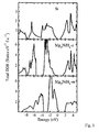
- Fig. 3.
- illustrates the total density of states (DOS) for Si, Mg2NiH4-c, and Mg2NiH4-m. The Fermi level is set to zero.
- Fig. 4.
- illustrates the orbital and site projected DOS for DOS for Si and Mg2NiH4-c. Fermi level is set at zero energy.
- Fig. 5.
- illustrates the total DOS for Mg2NiH4 -c doped with AlMg and LiMg along with that for bulk Mg2NiH4 -c. The Fermi level is set to zero.
- Fig. 6.
- illustrates the optical spectra for Mg2NiH4 -c doped with LiMg and AlMg as compared to those for undoped Mg2NiH4 -c.
- Fig. 7
- illustrates a schematic cross section of the component according to the invention.
- Fig. 8
- shows a table over effective masses (in units of the electron rest mass m0) of electrons mc and holes mh for some hydrides, conventional semiconductors and transparent conductive oxides (TCOs).
- Analysis of literature and our studies of electronic structure and optical properties of hydrides with/without defects and impurities shows that some hydrides are insulators with large fundamental band gap (see
Fig. 1). Figure 1 shows the fundamental band gap of a number of metal and complex hydrides: 1-5. MgH2; BeH2; LiAlH4; NaAlH4; NaAlH4; 6-10. KalH4; RbAlH4; CsAlH4; LiBH4; NaBH4; 11-15. KBH4; RbBH4; CsBH4; LiGaH4; NaGaH4; 16-20. KGaH4; RbGaH4; CsGaH4; Li3AlH6; Na3AlH6; 21-25. K3AlH6; LiMgH3; NaMgH3; KMgH3; RbMgH3; 26-30. CsMgH3; LiBeH3; NaBeH3; KBeH3; RbBeH3; 31-35. CsBeH3; BeAlH5; MgAlH ; CaAlH5; SrAlH5; 36-40. BaAlH5; MgB2H8; MgAl2H8; CaB2H8; CaAl2H8; 41-45. Ba6Mg7H26; BaMgH4; Ca19Mg8H54; Ca4Mg3H14; Ca4Mg4FeH63; 46-50. CaMgNiH4; Cs2MgH4; Cs3MgH5; K2MgH4; LiMg2RuH6; 51-55. Mg2RuH4; Mg3ReH7; Rb2MgH4; Rb3MgH5; Rb4Mg3H10; 56-60. SrMg2FeH8; SrMgH4; SrMgNiH4; Yb4Mg3H14; Sr2Mg3H10; 61-66 LiH; NaH; KH, RbH; CsH; CuH; 67-70 BaLiH3; CaCaH3; RbCaH3; SrLiH3., 71-76 α-AlH3, β-AlH3, γ-AlH3. Mg2NiH4 -c, Mg2NiH4-m, Mg2CoH5. With band gaps less than approximately 3 eV the materials are opaque while they are transparent above 3eV. The most desirable range is between 3 and 4 eV. - The calculated band gaps presented in
Fig. 1 are underestimated because of the well known deficiency of calculation method, density-functional theory (DFT). So, real band gaps are expected to be larger than those presented inFig. 1 . Analysis ofFig. 1 shows that Ca4Mg4FeH63, Mg2RuH4, CuH, BaLiH3 posses small band gaps <1.5 eV. Often, small band gap solids posses the feature of easy bipolar doping, i.e. to be doped with shallow donor and acceptors providing n- and p-type conductivities, respectively. One can design from such solids p-n-junction. Well dispersed nature of bottom-most conduction band and top-most valence bands show that these materials are expected to show good electrical conductivity. Such hydrides can present interest for electronic device applications, say as p-n junction based devices (solar cells, photodetectors, buffer layers, etc.). - Band structure studies for some of the hydrides (
Fig. 2 ) show that bottom-most CB and topmost VB of Si, Mg2NiH4 -c, and Mg2NiH4-m are well dispersive. Consequently, carrier transport through conduction band (CB) and/or valence band (VB) for these hydrides is possible. These analyses show that band structure of hydrides posses the feature required for current transport like semiconductors. - Total density of states (DOS) N(E) has been calculated (
Fig. 3 ). Analysis shows that the topmost VB is sufficiently wide and it does not present isolated sharp peaks. This feature indicates to significant role of covalence in chemical bonding, which is favorable for current transport through these compounds. Knowing the total density of states (DOS) N(E) calculated by DFT, effective DOS in the conduction band (CB) Nc and in the valence band (VB) Nv have been estimated

which have been used to calculate intrinsic carrier concentration ni
- Here E is the energy, Ec and Ev are the energies corresponding to bottommost CB and topmost VB. k is the Boltzmann constant and T is the temperature. V 0 is the volume of the unit cell and Eg = Ec - Ev is the fundamental band gap. Knowledge of ni allows to estimate diffusion potential of the p-n junction with concentration of shallow donors Nd and shallow acceptors Na

which is one of the important parameters of semiconductor p-n junction based devices. Using the values of N(E) and Eq. (1)-(3), effective DOS for CB (Nc) and VB (Nv) as well as intrinsic carrier concentration (ni ) have been calculated for Si, Mg2NiH4 -c, and Mg2NiH4-m for T=300 K (Table II). These values are close to those of Si. The small difference can be related to peculiarities of the band structure and fundamental band gap. - The orbital and site projected density of states (PDOS) and fat band analysis has been performed.
Figure 4 presents PDOS for Si and Mg2NiH4-c. Analysis showed that not only the bottommost CB, but also the topmost VB of most of the hydrides are mainly contributed from s-electrons. This is the distinguishing feature of hydrides compared to conventional semiconductors and TCOs where the topmost VB are commonly originated from p-/d-electrons and bottommost CB - from s-electrons. - One of the parameters characterizing transport properties of solids is carrier effective masses. Effective masses have been calculated for Si and Mg2NiH4 -c, and Mg2NiH4-m as illustrated in the table in
figure 8 . Analysis shows that the effective masses of hydrides are of the same order as those of the well known semiconductors such as Si and GaAs, TCOs ZnO and In2O3. The results indicate that electrical conductivity of hydrides can be the same as that of semiconductors and TCOs. - Application of a material as electric and optoelectronic devices critically depends on dopability, which can be limited by the following three main factors:
- (i) the desired shallow-level impurity may have a low solubility;
- (ii) even if it has good solubility, but its transition energy can be deep, so that at operating temperature the defect can not be ionized;
- (iii) even if the shallow level impurity posses good solubility, upon shifting the Fermi energy oppositely charged native defects or defect-impurity complexes can be formed.
- In this specification the issue (ii) of whether an impurity form shallow energy level in the band gap of hydrides.
- As the shallow-level defects and impurities can be the source for electrical conductivity of semiconductors, we have calculated electronic structure and optical properties of several hydrides.
Figure 5 presents total DOS for Mg2NiH4 -c with AlMg and LiMg. We found that AlMg (Figure 5 ) form states below the bottommost part of the CB of Mg2NiH4 -c. These shallow-donor-states are not isolated from the CB and can contribute to the n-type electrical conductivity. The defects such as LiMg form shallow acceptor states and can contribute to p-type electrical conductivity (Figure 5 ). - Doping can affect not only conductivity but also transparency. In order to establish this viewpoint we have studied absorption and reflectivity spectra of Mg2NiH4-c with AlMg and LiMg (
Fig. 6 ). FromFig. 5 it is seen that AlMg and LiMg doped Mg2NiH4-c is not transparent. The reason is that not only the fundamental, but also the second band gap of the hydride, which is the energy difference between the nearest two bottommost CB, is not sufficiently large. To consider these hydrides as TC materials the second band gap should be >3.1 eV. - In TCOs it is well known that one can easily bring in n-type conductivity, but the introduction of p-type conductivity is problematic. It follows from our results that high p-type doping level in hydrides shall not loose transparency, but can provide good conductivity, whereas high n-type doping leads to loss in transparency. This is one of the distinguishing features between TCOs and hydrides. The calculated formation energies for the Li(Al) doped Mg2NiH4-c is -0.20(+1.57) eV, which shows that the configuration with Li is stable, whereas that with Al is not stable.
- Knowledge of intrinsic carrier concentration and concentration of shallow acceptors and donors allows one to calculate by Eq. (4) diffusion potential VD . Below we perform such estimation for Mg2NiH4 -c. Assuming Nd ~1020cm-3 and Na ~1015cm-3 one can find that VD ~1.06 V.
- As can be seen from
Fig.1 large number of hydrides possess wide band gap and therefore can be used as transparent windows for wide variety of electronic devices such as solar cells, light emitting diodes etc. Thus, the wide band gap hydrides can be regarded as an alternative to such conventional transparent microelectronic materials as SiOx, SiNx or SiNx:H. Distinct from these transparent windows, hydrides have the advantage to provide good passivation of interfaces in semiconductor devices similar to that by the a-Si:H due to high concentration of hydrogen in their structure. More systematic investigations are necessary to prove this statement. - Although wide band gap hydrides can be conductive, as it was shown above, the doping limit for each concrete hydride material is not known yet and has to be studied systematically. In case if an effective high level doping and electrical conductivity can be realised for some of them along with transparency to the visible part of the solar spectra, they can be regarded as alternative to TCO materials. Nevertheless, at this stage of investigations it is possible to claim already that hydrides are more flexible materials than SiNx or TCOs, which are widely used as antireflection coatings in solar cells. As it is well known, optical properties of SiNx and TCOs and passivation of interface states shall be controlled by modulation of the nitrogen or oxygen stoichiometry, which is rather problematic. Upon using hydrides these features can relatively easily be controlled by hydrogen content only. Consequently, formation of nano-dots and other nano-structures in hydrides can be realized more easily than those in SiNx and TCOs. Furthermore, structural and morphological modifications of hydrides can be done at much lower temperatures and pressures than SiNx and TCOs. Hence, hydrides can be more suitable for low temperature synthesis technologies.
- The usage of TCOs in some devices results in the formation of an intermediate oxide layer, large band-offset, and defect states, which can limit the device performance. If hydrides would be used instead of the TCOs, then no oxide layer would be formed and there is no need in using buffer layer. Large band-offset can be prevented by reducing the band gap of the hydrides, which is much easier than that in oxides. Furthermore, hydrogen diffusion from hydrides into semiconductors can be useful to passivate defect states at the interface and increase their conductivity those are important for improving the device performance. Hydrides can also be regarded as a natural alternative to SiNx and TCOs in case of any low temperature technology.
- Smaller band gap hydrides with well dispersive bottommost conduction band and topmost valence band can be useful to replace semiconductor devices such as, say, solar cells. From this point of view, hydrides can be regarded as novel class of solar cells. The crystalline nature and light weight of hydrides, as well as small concentration of defects between active solar cell and TCO present interest for third generation photovoltaics. World wide lot of attention is currently focused on developing environmentally friendly technologies, alternative energy sources, improving the performance of solar cells etc. and our finding is directly relevant to these activities. It has to be noted that hydrides in most cases are much lighter than conventional semiconductors, and hydrogen is the most abundant element in the universe. Consequently, hydrides are of great interest for terrestrial and space applications of solar cells, and also hydrides have large potential for applications in bio-compatible semiconducting devices.
- The component according to the invention is illustrated in
figure 7 and is preferable produced by positioning at least onemetal layer substrate 4, and acapping layer 1 on top of themetal layer - After the deposition of the
capping layer 1 the component is hydrogenated by subjecting the component to agas flow 5 comprising hydrogen, as will be discussed more in detail below. Resulting from this is a component comprising acapping layer 1, a dopedmetal hydride layer figure 1 twometal hydride layers - A principle scheme for fabrication of individual n- or p-type metal hydride layers or a p-n (n-p) junction based metal hydride structures can be described as follows:
- (i) Deposition of an individual metal layer with an appropriate metal composition (co-doped by some elements, see examples below), which provides formation of the p-type hydride after the hydrogenation. This process can be realized using any sputtering method: magnetron, thermal evaporation, e-beam evaporation etc. as well as by any chemical deposition methods. In case of a sputtering process, deposition can be done from one (one target consists of a required composition) or several individual targets (co-sputtering process). Deposition can be done on any substrate (metal, ceramics, semiconductor, polymer etc.) in a temperature interval from room-temperature up to the minimum value of the melting temperature of the sputtered metal composition or the substrate. The thickness of the layer, depending on the applications, can be different:
- from few nm to few µm.
- In case of fabrication of a n-p junction metal hydride structure, one addition metal layer has to be deposited as described below.
- (ii) The same sputtering process can be applied for deposition of a metal layer (co-doped) with an appropriate composition, which provides formation of an n-type layer after the hydrogenation (see examples below).
- (iii) For the formation of a transistor-like structure (n-p-n or p-n-p), deposition of a third corresponding layer after the process (ii) is required.
- (iv) After processes described in (i),(ii) and (iii) a capping Pd or Ni layers with thickness 3-20 nm have to be deposited on an individual metallic layer (after process (i)) or on a metallic stack (after processes (ii) and (iii)). The Pd(Ni) layers serve as catalytic ones to provide a hydrogenation of metallic based structures to convert them into metal hydrides. Thus, these layers work as a membrane that allows passing of hydrogen through them towards to metallic layers with different composition.
- (v) The hydrogenation process can be performed by exposing the final films to a dry gas stream (pure H2 or H2 containing forming gas (a mixture of H2 with a noble gas)). Some details of the dry hydrogenation are given in article by T.J. Richardson, J.L. Slack, R.D. Armitage, R. Kostecki, B. Farangis, M.D. Rubin, "Switchable mirrors based on nickel-magnesium films", Appl. Phys. Lett. Vol. 78, No 20 (2001) p.3047-3049. The hydrogenation process can be done at temperatures between room temperature and the stability temperature of a given metal hydride. Moreover, the hydrogenation can be performed in an electrolyte solution, as described in an article by E.S. Matveeva, R.J. Ortega Ramiro, A. Sanchez Bolinchez, C. Ferrer Limenez, V.P. Parkhutik, "Design and operational conditions of small electrochemical cell for optical switching employing hydrogenation of Pd/Y structure", Sensors and Actuators B 84 (2002) p. 83-90. In this case hydrogenation can be performed at temperatures between room temperature and 100°C. The hydrogenation has to be done up to the stage, at which a given metal composition or whole metal multi-layer structure is converted into a semiconductor ones completely. The conversion (hydrogenation) time depend on the composition of each individual metal layer, thickness of metallic layers, hydrogenation temperature, hydrogen (forming gas) pressure etc.
- An alternative production method may be performed by growing the layers as hydrides, which will reduce the stress in the material which occurs when it is loaded with hydrogen after the deposition. A more detailed description is given in the thesis of Ingrid A.M.E. Giebels "Shining light on magnesium based switchable mirrors" ISBN 90-9018547-X, section 2.2.1 where a GdMg-H5 layer is produced by co-sputtering of the metals in a hydrogen/argon atmosphere at room temperature. In this case also the capping layer may be omitted during production. The abovementioned thesis in sections 2.2.2 and 2.2.3 also discloses other production methods incorporating In-Situ and Ex-Situ hydrogen loading. A combination of the production methods may also be contemplated, where the layers are grown as hydrate metals, and additional hydrogen are loaded afterward. This is discussed in section 5.14 in the thesis of Ruud Westerwaal, "Growth, microstructure and hydrogenation of Pd-catalyzed complex metal hydride thin films", ISBN-978 90 8659 071 1.
- Due to a possibility to fabricate metal hydrides with any desirable band gap, which depends on the composition (including the hydrogen content) the individual n- or p-type metal hydrides layers can be utilized for instance as buffer layers for heterojunction devices, such as solar cells. In this case the device structures look like follows:
- (i) Antireflection coating/Pd/Ni) 1/n-(p-type)
metal hydride 2/p-(n-type)solar cell base: (Si, In-Ga-Cu-Se(S), etc) 3/back side metallization 7;
or - (ii) Antireflection coating/Pd/Ni) 1/n-(p-type)
metal hydride 2/p-(n-type)solar cell base: (Si, In-Ga-Cu-Se(S), etc) 3/ p-(n-type) metal hydride (not shown)/Pd(i) 4/ back side metallization 7; - The n-type/p-type metal hydride stack can also be utilized as a diode, which is a basic structure of several microelectronic devices, including solar cells. In the later case the metal hydride solar cell structures look as follows: Antireflection coating 1/n-type(p-type) metal hydride (emitter) 2/p-type(n-type) metal hydride
solar cell base 3/ Pd(Ni) 4/back side metallization 7; - A number of different metal hydrides may be used as n- and p-type semiconductors. Some examples are mentioned below:
- Mg2NiH4-c
- n-type conductivity provided by Al doping, which being in a Mg site leads to the formation of Mg2NiH4-c:AlMg composition. Concentration of Al atoms as the Mg substitution dopants for the Mg2NiH4-c composition can be varied from 1015 to 1022 atom/cm3.
- p-type conductivity provided by Li in Mg substitution position. Concentration of Li atoms as the H substitution dopants for the Mg2NiH4-c composition can be varied from 1015 to 1022 atom/cm3.
- AlH3 (see the abovementioned article by S. Karazhanov et al, published in Phys. Stat. Sol. "hydride electronics")
- n-type conductivity provided by group-IV/-II atoms (C,Si, etc.Be, Mg, etc.) substituting Al.
- p-type conductivity provided by Ca atom doping. In this case Ca substitutes Al.
- The concentration of all foreign atoms, which provide the n- or p-type conductivity in AlH3 structure, can be varied from 1015 to 1022 atom/cm3.
- Other combinations of metals and dopants may be contemplated, e.g. combinations of the AlHx and NgNiHx materials mentioned above, thus providing any combinations of n-p, p-n, p-p or n-n junctions, as well as three layered components such as n-p-n and p-n-p constituting transistors. The materials are chosen depending on their stability, especially related to temperature and the band gap as well as the compatibility with other materials in the component and connected instruments and conductors. It is also possible to use materials having amorphous properties with the selected concentrations of hydrogen.
- Electrical couplings to conductor leads 6,7 for utilizing the component in an electronic system may also be of different types depending on the compatibility. In general there it is an advantage related to the use of metal hydrides as semiconductors that they provide good electrical contact with other materials and conductor leads. The electrical coupling points may be chosen e.g. to the top
metal hydride surface 2 and to thesubstrate 4. - The
substrate 4 is made by any material being compatible with the materials of the deposited layers, such as metal, ceramic, glass, polymers, etc, the choice also depending on the need for e.g. an electrically conductive substrate or for providing electrical conductors on or through the substrate. Thesubstrate 4 may also be a metal or metal to be hydrogenated through the production process, thus being part of the active component. - Thus the component according to the inventions involves a layered structure comprising at least one p- or n- type metal hydride. In the preferred embodiment the component incorporates at least two layers, e.g. providing a p-n junction or three layers providing a n-p-n or p-n-p junction, but other solutions may be contemplated, depending on the use, for example an n-n' configuration.
- Usually the component will include a protective top layer, e.g. a TCO and a lower substrate. Between the layers amorphous layers of metal hydrides or silicon may be used, so as to act as stress relieves or buffer layers, but this may not be necessary if two layers are compatible. A possible component according to the invention for use in solar cells could thus be comprised from the bottom and up by a
conductive metal substrate 4, a p-typemetal hydride layer 3, an n-typemetal hydride layer 2, and aTCO 1 on top, withconductors TCO layer 1 andmetal substrate 4. Depending on the available materials and their band gaps other structures may also be possible, as mentioned above constituting p-n-p structures etc. - To summarize the invention thus relates to an electronic semiconductive component comprising at least one layer of a p-type or n-type material, wherein said p- or n-type material is constituted by a metal hydride having a chosen dopant. According to the preferred embodiment the component comprises both a p-type and an n-type material constituting a p-n junction, wherein at least one of said p- and n-type materials is constituted by a metal hydride having a chosen dopant. Thus effectively constituting a diode, which can be used as a solar cell.
- A number of material may be used for making the n-type material in the component, such as having at least one following materials Mg2NiH4 -c with Al atom doping in a concentration of 1015 to 1022 atoms/cm3, MgH2 with Al atom doping in a concentration of 1015 to 1022 atoms/cm3 or MgH2 with Cs atom doping in a concentration of 1015 to 1022 atoms/cm3. Another possible n-type material is made from AlH3 with atom doping from group IV/II atoms, eg. C,Si,Be,Mg etc in a concentration of 1015 to 1022 atoms/cm3.
- Similarily p-type materials may for example be provided by using a material made from Mg2NiH4-c with Li atom doping in a concentration of 1015 to 1022 atoms/cm3, MgH2 with Li atom doping in a concentration of 1015 to 1022 atoms/cm3, or at least one following materials AlH3 with Ca atom doping in a concentration of 1015 to 1022 atoms/cm3.
- In addition to the p-n junction a third layer may be added, for example making a p-n-p og n-p-n device.
- The component may be produced in different ways for example by ex-situ or in-situ deposition or sputtering techniques. The ex-situ deposition method comprising the steps of depositing at least one layer constituted by a chosen metal having a chosen dopant on a substrate, said dopant providing a n- or p-type conductivity after hydrogenation, providing a capping layer on said at least one layer, and exposing the layers and capping to a gas stream containing a chosen fraction of hydrogen. This method may also include depositing of two metal layers, one of which providing an n-type semiconductor after hydrogenation and the second providing a p-type semiconductor after hydrogenation, thus providing a p-n junction, and depositing a third metal layer providing a second p-n or n-p junction after hydrogenation.
- The in-situ production method may comprise the steps of depositing at least one first layer constituted by a chosen metal having a chosen dopant on a substrate, the deposition being performed by a sputtering process in an atmosphere constituted by hydrogen and a nobel gas, e.g. argon, thus depositing a hydrogenated doped metal layer, the dopant providing a n- or p-type conductivity.
- As with the ex-situ method this may also include a second step of depositing a second layer with a second dopant being different from said first dopant, as well as a third step adding a third layer. A combination of the two methods may also be used by including a step of depositing a capping layer and exposing said component to a gas stream containing a chosen fraction of hydrogen for additional hydrogen loading of the material.
Claims (15)
- Electronic semiconductive component comprising at least one layer of a p-type or n-type material, characterized in that one of said at least one layer of p- or n-type material is constituted by a metal hydride having a chosen dopant.
- Component according to claim 1 comprising a p-type and an n-type material constituting a p-n junction, wherein at least one of said p- and n-type materials is constituted by a metal hydride having a chosen dopant.
- Component according to claim 1, wherein the material is an n-type material having at least one following materials: Mg2NiH4 -c with Al atom doping in a concentration of 1015 to 1022 atoms/cm3, MgH2 with Al atom doping in a concentration of 1015 to 1022 atoms/cm3 or MgH2 with Cs atom doping in a concentration of 1015 to 1022 atoms/cm3.
- Component according to claim 1, wherein the material is a p-type material made from Mg2NiH4 -c with Li atom doping in a concentration of 1015 to 1022 atoms/cm3, MgH2 with Li atom doping in a concentration of 1015 to 1022 atoms/cm3.
- Component according to claim 1, wherein the material is a p-type material of at least one following materials AlH3 with Ca atom doping in a concentration of 1015 to 1022 atoms/cm3.
- Component according to claim 1, wherein the material is an n-type material made from Mg2NiH4 with atom doping from group I/III atoms, eg. Li/Al, etc in a concentration of 1015 to 1022 atoms/cm3.
- Component according to claim 2, also including a third material of a p-type providing a p-n junction with said n-type material, the component thus being a p-n-p device.
- Component according to claim 2, also including a third material of a n-type providing a p-n junction with said n-type material, the component thus being a n-p-n device.
- Use of a component according to claim 1 as a solar cell.
- Method for producing a component according to claim 1 including a semiconducting metal hydride, comprising the steps of depositing at least one layer constituted by a chosen metal having a chosen dopant on a substrate, said dopant providing a n- or p-type conductivity after hydrogenation, providing a capping layer on said at least one layer, and exposing the layers and capping to a gas stream containing a chosen fraction of hydrogen.
- Method according to claim 10, wherein it includes depositing of two metal layers, one of which providing an n-type semiconductor after hydrogenation and the second providing a p-type semiconductor after hydrogenation, thus providing a p-n junction.
- Method according to claim 10, wherein it includes depositing a third metal layer providing a second p-n or n-p junction after hydrogenation.
- Method for producing a component according to claim 1 including a semiconducting metal hydride, comprising the steps of depositing at least one first layer constituted by a chosen metal having a chosen dopant on a substrate, the deposition being performed by a sputtering process in an atmosphere constituted by hydrogen and a noble gas, e.g. argon, thus depositing a hydrogenated doped metal layer, the dopant providing a n- or p-type conductivity.
- Method according to claim 13, including a second step of depositing a second layer with a second dopant being different from said first dopant.
- Method according to claim 13, including a step of depositing a capping layer and exposing said component to a gas stream containing a chosen fraction of hydrogen for additional hydrogen loading of the material.
Priority Applications (1)
| Application Number | Priority Date | Filing Date | Title |
|---|---|---|---|
| EP12193329A EP2562817A1 (en) | 2008-02-11 | 2009-02-09 | Semiconducting component |
Applications Claiming Priority (3)
| Application Number | Priority Date | Filing Date | Title |
|---|---|---|---|
| US6400408P | 2008-02-11 | 2008-02-11 | |
| NO20080769A NO342873B1 (en) | 2008-02-11 | 2008-02-12 | Semiconductor Component |
| PCT/NO2009/000045 WO2009102213A1 (en) | 2008-02-11 | 2009-02-09 | Metal hybride semiconducting component |
Related Child Applications (1)
| Application Number | Title | Priority Date | Filing Date |
|---|---|---|---|
| EP12193329.5 Division-Into | 2012-11-20 |
Publications (3)
| Publication Number | Publication Date |
|---|---|
| EP2248177A1 EP2248177A1 (en) | 2010-11-10 |
| EP2248177B1 true EP2248177B1 (en) | 2012-11-21 |
| EP2248177B8 EP2248177B8 (en) | 2013-01-02 |
Family
ID=41091754
Family Applications (2)
| Application Number | Title | Priority Date | Filing Date |
|---|---|---|---|
| EP12193329A Withdrawn EP2562817A1 (en) | 2008-02-11 | 2009-02-09 | Semiconducting component |
| EP09709825A Not-in-force EP2248177B8 (en) | 2008-02-11 | 2009-02-09 | Metal hydride semiconducting component |
Family Applications Before (1)
| Application Number | Title | Priority Date | Filing Date |
|---|---|---|---|
| EP12193329A Withdrawn EP2562817A1 (en) | 2008-02-11 | 2009-02-09 | Semiconducting component |
Country Status (4)
| Country | Link |
|---|---|
| US (2) | US9461123B2 (en) |
| EP (2) | EP2562817A1 (en) |
| NO (1) | NO342873B1 (en) |
| WO (1) | WO2009102213A1 (en) |
Families Citing this family (2)
| Publication number | Priority date | Publication date | Assignee | Title |
|---|---|---|---|---|
| NO342873B1 (en) | 2008-02-11 | 2018-08-20 | Inst Energiteknik | Semiconductor Component |
| US10658532B2 (en) * | 2016-02-11 | 2020-05-19 | Flisom Ag | Fabricating thin-film optoelectronic devices with added rubidium and/or cesium |
Family Cites Families (9)
| Publication number | Priority date | Publication date | Assignee | Title |
|---|---|---|---|---|
| FR2303385A1 (en) * | 1975-03-03 | 1976-10-01 | Radiotechnique Compelec | NEW PROCESS FOR MANUFACTURING SEMICONDUCTOR BODIES |
| US4710786A (en) * | 1978-03-16 | 1987-12-01 | Ovshinsky Stanford R | Wide band gap semiconductor alloy material |
| EG18056A (en) * | 1986-02-18 | 1991-11-30 | Solarex Corp | Dispositif feedstock materials useful in the fabrication of hydrogenated amorphous silicon alloys for photo-voltaic devices and other semiconductor devices |
| AUPM483494A0 (en) * | 1994-03-31 | 1994-04-28 | Pacific Solar Pty Limited | Multiple layer thin film solar cells |
| US5719076A (en) * | 1996-04-24 | 1998-02-17 | United Solar Systems Corporation | Method for the manufacture of semiconductor devices with optimized hydrogen content |
| US6146608A (en) * | 1997-11-24 | 2000-11-14 | Advanced Technology Materials, Inc. | Stable hydride source compositions for manufacture of semiconductor devices and structures |
| CA2301252A1 (en) * | 2000-03-17 | 2001-09-17 | Hydro-Quebec | Method for producing gaseous hydrogen by chemical reaction of metals or metal hydrides subjected to intense mechanical deformations |
| CN1199949C (en) * | 2003-06-25 | 2005-05-04 | 山东大学 | High-purity 8-hydroxyquinoline aluminium group compound, preparation method and use thereof |
| NO342873B1 (en) | 2008-02-11 | 2018-08-20 | Inst Energiteknik | Semiconductor Component |
-
2008
- 2008-02-12 NO NO20080769A patent/NO342873B1/en unknown
-
2009
- 2009-02-09 US US12/867,070 patent/US9461123B2/en active Active
- 2009-02-09 EP EP12193329A patent/EP2562817A1/en not_active Withdrawn
- 2009-02-09 WO PCT/NO2009/000045 patent/WO2009102213A1/en not_active Ceased
- 2009-02-09 EP EP09709825A patent/EP2248177B8/en not_active Not-in-force
-
2016
- 2016-03-28 US US15/082,160 patent/US10461160B2/en active Active
Also Published As
| Publication number | Publication date |
|---|---|
| NO342873B1 (en) | 2018-08-20 |
| US20100319760A1 (en) | 2010-12-23 |
| US10461160B2 (en) | 2019-10-29 |
| EP2248177A1 (en) | 2010-11-10 |
| NO20080769L (en) | 2009-08-12 |
| US9461123B2 (en) | 2016-10-04 |
| WO2009102213A1 (en) | 2009-08-20 |
| US20160211391A1 (en) | 2016-07-21 |
| EP2248177B8 (en) | 2013-01-02 |
| EP2562817A1 (en) | 2013-02-27 |
Similar Documents
| Publication | Publication Date | Title |
|---|---|---|
| Gupta et al. | Recent advances in materials design using atomic layer deposition for energy applications | |
| Mailoa et al. | A 2-terminal perovskite/silicon multijunction solar cell enabled by a silicon tunnel junction | |
| CN101960618B (en) | Low-cost solar cells and methods for their production | |
| AU2015304774B2 (en) | System and method based on low-pressure chemical vapor deposition for fabricating perovskite film | |
| Masudy-Panah et al. | Reduction of Cu-rich interfacial layer and improvement of bulk CuO property through two-step sputtering for p-CuO/n-Si heterojunction solar cell | |
| Wan et al. | A magnesium/amorphous silicon passivating contact for n-type crystalline silicon solar cells | |
| Chua et al. | Enhancement of the open circuit voltage of Cu2O/Ga2O3 heterojunction solar cells through the mitigation of interfacial recombination | |
| CN109923687A (en) | Solar battery and manufacturing method comprising metal oxide buffer layer | |
| EP0233613B1 (en) | Deposition feedstock and dopant materials useful in the fabrication of hydrogenated amorphous silicon alloys for photovoltaic devices and other semiconductor devices | |
| Dutta et al. | Low-temperature UV ozone-treated high efficiency radial pn junction solar cells: N-Si NW arrays embedded in a p-Si matrix | |
| Xu et al. | Mitigating voltage loss in efficient CsPbI2Br all-inorganic perovskite solar cells via metal ion-doped ZnO electron transport layer | |
| Park et al. | Amorphous TiO2 Passivating Contacts for Cu (In, Ga)(S, Se) 2 Ultrathin Solar Cells: Defect‐State‐Mediated Hole Conduction | |
| Bharwal et al. | Influence of sodium concentration on the optoelectronic properties of silicon clathrate films | |
| Kang et al. | Carbon-doped GaAs single junction solar microcells grown in multilayer epitaxial assemblies | |
| Yu et al. | Enhancing poly-Si contact through a highly conductive and ultra-thin TiN layer for high-efficiency passivating contact silicon solar cells | |
| US20110146784A1 (en) | Photovoltaic device back contact | |
| CN103210499B (en) | Electrical contact | |
| US10461160B2 (en) | Semiconducting component | |
| Rahman | Cadmium telluride (CdTe) thin film solar cells | |
| Jang et al. | Achieving over 10% device efficiency in Cu2ZnSn (S, Se) 4 thin-film solar cells with modifications of window layer properties | |
| Manjunatha et al. | Carrier selective metal-oxides for self-doped silicon nanowire solar cells | |
| Wang et al. | Enhanced solar hydrogen production by manipulating the spatial distribution of Pt catalyst onto Si micro-pyramid arrays | |
| Liu et al. | Improved device performance of Si-based heterojunction solar cells by using phosphorus doped Si nanocrystals embedded in SiC host matrix | |
| US7368658B1 (en) | High efficiency diamond solar cells | |
| Camacho-Espinosa et al. | CHClF2 gas mixtures to activate all-sputtered CdS/CdTe solar cells |
Legal Events
| Date | Code | Title | Description |
|---|---|---|---|
| PUAI | Public reference made under article 153(3) epc to a published international application that has entered the european phase |
Free format text: ORIGINAL CODE: 0009012 |
|
| 17P | Request for examination filed |
Effective date: 20100910 |
|
| AK | Designated contracting states |
Kind code of ref document: A1 Designated state(s): AT BE BG CH CY CZ DE DK EE ES FI FR GB GR HR HU IE IS IT LI LT LU LV MC MK MT NL NO PL PT RO SE SI SK TR |
|
| AX | Request for extension of the european patent |
Extension state: AL BA RS |
|
| DAX | Request for extension of the european patent (deleted) | ||
| GRAP | Despatch of communication of intention to grant a patent |
Free format text: ORIGINAL CODE: EPIDOSNIGR1 |
|
| GRAS | Grant fee paid |
Free format text: ORIGINAL CODE: EPIDOSNIGR3 |
|
| GRAA | (expected) grant |
Free format text: ORIGINAL CODE: 0009210 |
|
| AK | Designated contracting states |
Kind code of ref document: B1 Designated state(s): AT BE BG CH CY CZ DE DK EE ES FI FR GB GR HR HU IE IS IT LI LT LU LV MC MK MT NL NO PL PT RO SE SI SK TR |
|
| REG | Reference to a national code |
Ref country code: GB Ref legal event code: FG4D |
|
| REG | Reference to a national code |
Ref country code: CH Ref legal event code: EP |
|
| REG | Reference to a national code |
Ref country code: AT Ref legal event code: REF Ref document number: 585465 Country of ref document: AT Kind code of ref document: T Effective date: 20121215 |
|
| REG | Reference to a national code |
Ref country code: IE Ref legal event code: FG4D |
|
| REG | Reference to a national code |
Ref country code: DE Ref legal event code: R096 Ref document number: 602009011352 Country of ref document: DE Effective date: 20130117 |
|
| REG | Reference to a national code |
Ref country code: NL Ref legal event code: VDEP Effective date: 20121121 |
|
| REG | Reference to a national code |
Ref country code: AT Ref legal event code: MK05 Ref document number: 585465 Country of ref document: AT Kind code of ref document: T Effective date: 20121121 |
|
| REG | Reference to a national code |
Ref country code: LT Ref legal event code: MG4D |
|
| PG25 | Lapsed in a contracting state [announced via postgrant information from national office to epo] |
Ref country code: LT Free format text: LAPSE BECAUSE OF FAILURE TO SUBMIT A TRANSLATION OF THE DESCRIPTION OR TO PAY THE FEE WITHIN THE PRESCRIBED TIME-LIMIT Effective date: 20121121 Ref country code: ES Free format text: LAPSE BECAUSE OF FAILURE TO SUBMIT A TRANSLATION OF THE DESCRIPTION OR TO PAY THE FEE WITHIN THE PRESCRIBED TIME-LIMIT Effective date: 20130304 Ref country code: NO Free format text: LAPSE BECAUSE OF FAILURE TO SUBMIT A TRANSLATION OF THE DESCRIPTION OR TO PAY THE FEE WITHIN THE PRESCRIBED TIME-LIMIT Effective date: 20130221 Ref country code: HR Free format text: LAPSE BECAUSE OF FAILURE TO SUBMIT A TRANSLATION OF THE DESCRIPTION OR TO PAY THE FEE WITHIN THE PRESCRIBED TIME-LIMIT Effective date: 20121121 Ref country code: SE Free format text: LAPSE BECAUSE OF FAILURE TO SUBMIT A TRANSLATION OF THE DESCRIPTION OR TO PAY THE FEE WITHIN THE PRESCRIBED TIME-LIMIT Effective date: 20121121 Ref country code: FI Free format text: LAPSE BECAUSE OF FAILURE TO SUBMIT A TRANSLATION OF THE DESCRIPTION OR TO PAY THE FEE WITHIN THE PRESCRIBED TIME-LIMIT Effective date: 20121121 |
|
| PG25 | Lapsed in a contracting state [announced via postgrant information from national office to epo] |
Ref country code: LV Free format text: LAPSE BECAUSE OF FAILURE TO SUBMIT A TRANSLATION OF THE DESCRIPTION OR TO PAY THE FEE WITHIN THE PRESCRIBED TIME-LIMIT Effective date: 20121121 Ref country code: SI Free format text: LAPSE BECAUSE OF FAILURE TO SUBMIT A TRANSLATION OF THE DESCRIPTION OR TO PAY THE FEE WITHIN THE PRESCRIBED TIME-LIMIT Effective date: 20121121 Ref country code: GR Free format text: LAPSE BECAUSE OF FAILURE TO SUBMIT A TRANSLATION OF THE DESCRIPTION OR TO PAY THE FEE WITHIN THE PRESCRIBED TIME-LIMIT Effective date: 20130222 Ref country code: BE Free format text: LAPSE BECAUSE OF FAILURE TO SUBMIT A TRANSLATION OF THE DESCRIPTION OR TO PAY THE FEE WITHIN THE PRESCRIBED TIME-LIMIT Effective date: 20121121 Ref country code: PT Free format text: LAPSE BECAUSE OF FAILURE TO SUBMIT A TRANSLATION OF THE DESCRIPTION OR TO PAY THE FEE WITHIN THE PRESCRIBED TIME-LIMIT Effective date: 20130321 Ref country code: PL Free format text: LAPSE BECAUSE OF FAILURE TO SUBMIT A TRANSLATION OF THE DESCRIPTION OR TO PAY THE FEE WITHIN THE PRESCRIBED TIME-LIMIT Effective date: 20121121 |
|
| PG25 | Lapsed in a contracting state [announced via postgrant information from national office to epo] |
Ref country code: AT Free format text: LAPSE BECAUSE OF FAILURE TO SUBMIT A TRANSLATION OF THE DESCRIPTION OR TO PAY THE FEE WITHIN THE PRESCRIBED TIME-LIMIT Effective date: 20121121 |
|
| PG25 | Lapsed in a contracting state [announced via postgrant information from national office to epo] |
Ref country code: BG Free format text: LAPSE BECAUSE OF FAILURE TO SUBMIT A TRANSLATION OF THE DESCRIPTION OR TO PAY THE FEE WITHIN THE PRESCRIBED TIME-LIMIT Effective date: 20130221 Ref country code: SK Free format text: LAPSE BECAUSE OF FAILURE TO SUBMIT A TRANSLATION OF THE DESCRIPTION OR TO PAY THE FEE WITHIN THE PRESCRIBED TIME-LIMIT Effective date: 20121121 Ref country code: EE Free format text: LAPSE BECAUSE OF FAILURE TO SUBMIT A TRANSLATION OF THE DESCRIPTION OR TO PAY THE FEE WITHIN THE PRESCRIBED TIME-LIMIT Effective date: 20121121 Ref country code: CZ Free format text: LAPSE BECAUSE OF FAILURE TO SUBMIT A TRANSLATION OF THE DESCRIPTION OR TO PAY THE FEE WITHIN THE PRESCRIBED TIME-LIMIT Effective date: 20121121 Ref country code: DK Free format text: LAPSE BECAUSE OF FAILURE TO SUBMIT A TRANSLATION OF THE DESCRIPTION OR TO PAY THE FEE WITHIN THE PRESCRIBED TIME-LIMIT Effective date: 20121121 |
|
| PG25 | Lapsed in a contracting state [announced via postgrant information from national office to epo] |
Ref country code: RO Free format text: LAPSE BECAUSE OF FAILURE TO SUBMIT A TRANSLATION OF THE DESCRIPTION OR TO PAY THE FEE WITHIN THE PRESCRIBED TIME-LIMIT Effective date: 20121121 Ref country code: NL Free format text: LAPSE BECAUSE OF FAILURE TO SUBMIT A TRANSLATION OF THE DESCRIPTION OR TO PAY THE FEE WITHIN THE PRESCRIBED TIME-LIMIT Effective date: 20121121 Ref country code: IT Free format text: LAPSE BECAUSE OF FAILURE TO SUBMIT A TRANSLATION OF THE DESCRIPTION OR TO PAY THE FEE WITHIN THE PRESCRIBED TIME-LIMIT Effective date: 20121121 |
|
| PLBE | No opposition filed within time limit |
Free format text: ORIGINAL CODE: 0009261 |
|
| STAA | Information on the status of an ep patent application or granted ep patent |
Free format text: STATUS: NO OPPOSITION FILED WITHIN TIME LIMIT |
|
| PG25 | Lapsed in a contracting state [announced via postgrant information from national office to epo] |
Ref country code: MC Free format text: LAPSE BECAUSE OF NON-PAYMENT OF DUE FEES Effective date: 20130228 |
|
| REG | Reference to a national code |
Ref country code: CH Ref legal event code: PL |
|
| 26N | No opposition filed |
Effective date: 20130822 |
|
| PG25 | Lapsed in a contracting state [announced via postgrant information from national office to epo] |
Ref country code: CH Free format text: LAPSE BECAUSE OF NON-PAYMENT OF DUE FEES Effective date: 20130228 Ref country code: LI Free format text: LAPSE BECAUSE OF NON-PAYMENT OF DUE FEES Effective date: 20130228 |
|
| REG | Reference to a national code |
Ref country code: IE Ref legal event code: MM4A |
|
| REG | Reference to a national code |
Ref country code: DE Ref legal event code: R097 Ref document number: 602009011352 Country of ref document: DE Effective date: 20130822 |
|
| PG25 | Lapsed in a contracting state [announced via postgrant information from national office to epo] |
Ref country code: IE Free format text: LAPSE BECAUSE OF NON-PAYMENT OF DUE FEES Effective date: 20130209 |
|
| PG25 | Lapsed in a contracting state [announced via postgrant information from national office to epo] |
Ref country code: MT Free format text: LAPSE BECAUSE OF FAILURE TO SUBMIT A TRANSLATION OF THE DESCRIPTION OR TO PAY THE FEE WITHIN THE PRESCRIBED TIME-LIMIT Effective date: 20121121 |
|
| PG25 | Lapsed in a contracting state [announced via postgrant information from national office to epo] |
Ref country code: TR Free format text: LAPSE BECAUSE OF FAILURE TO SUBMIT A TRANSLATION OF THE DESCRIPTION OR TO PAY THE FEE WITHIN THE PRESCRIBED TIME-LIMIT Effective date: 20121121 Ref country code: CY Free format text: LAPSE BECAUSE OF FAILURE TO SUBMIT A TRANSLATION OF THE DESCRIPTION OR TO PAY THE FEE WITHIN THE PRESCRIBED TIME-LIMIT Effective date: 20121121 |
|
| PG25 | Lapsed in a contracting state [announced via postgrant information from national office to epo] |
Ref country code: HU Free format text: LAPSE BECAUSE OF FAILURE TO SUBMIT A TRANSLATION OF THE DESCRIPTION OR TO PAY THE FEE WITHIN THE PRESCRIBED TIME-LIMIT; INVALID AB INITIO Effective date: 20090209 Ref country code: MK Free format text: LAPSE BECAUSE OF FAILURE TO SUBMIT A TRANSLATION OF THE DESCRIPTION OR TO PAY THE FEE WITHIN THE PRESCRIBED TIME-LIMIT Effective date: 20121121 Ref country code: LU Free format text: LAPSE BECAUSE OF NON-PAYMENT OF DUE FEES Effective date: 20130209 |
|
| REG | Reference to a national code |
Ref country code: FR Ref legal event code: PLFP Year of fee payment: 8 |
|
| PG25 | Lapsed in a contracting state [announced via postgrant information from national office to epo] |
Ref country code: IS Free format text: LAPSE BECAUSE OF FAILURE TO SUBMIT A TRANSLATION OF THE DESCRIPTION OR TO PAY THE FEE WITHIN THE PRESCRIBED TIME-LIMIT Effective date: 20121121 |
|
| REG | Reference to a national code |
Ref country code: FR Ref legal event code: PLFP Year of fee payment: 9 |
|
| REG | Reference to a national code |
Ref country code: FR Ref legal event code: PLFP Year of fee payment: 10 |
|
| PGFP | Annual fee paid to national office [announced via postgrant information from national office to epo] |
Ref country code: DE Payment date: 20240212 Year of fee payment: 16 Ref country code: GB Payment date: 20240214 Year of fee payment: 16 |
|
| PGFP | Annual fee paid to national office [announced via postgrant information from national office to epo] |
Ref country code: FR Payment date: 20240221 Year of fee payment: 16 |
|
| REG | Reference to a national code |
Ref country code: DE Ref legal event code: R079 Ref document number: 602009011352 Country of ref document: DE Free format text: PREVIOUS MAIN CLASS: H01L0029240000 Ipc: H10D0062800000 |
|
| REG | Reference to a national code |
Ref country code: DE Ref legal event code: R119 Ref document number: 602009011352 Country of ref document: DE |
|
| GBPC | Gb: european patent ceased through non-payment of renewal fee |
Effective date: 20250209 |
|
| PG25 | Lapsed in a contracting state [announced via postgrant information from national office to epo] |
Ref country code: DE Free format text: LAPSE BECAUSE OF NON-PAYMENT OF DUE FEES Effective date: 20250902 |
|
| PG25 | Lapsed in a contracting state [announced via postgrant information from national office to epo] |
Ref country code: GB Free format text: LAPSE BECAUSE OF NON-PAYMENT OF DUE FEES Effective date: 20250209 |
|
| PG25 | Lapsed in a contracting state [announced via postgrant information from national office to epo] |
Ref country code: FR Free format text: LAPSE BECAUSE OF NON-PAYMENT OF DUE FEES Effective date: 20250228 |