EP2248172B1 - Resistor triggered electrostatic discharge protection - Google Patents
Resistor triggered electrostatic discharge protection Download PDFInfo
- Publication number
- EP2248172B1 EP2248172B1 EP09715944.6A EP09715944A EP2248172B1 EP 2248172 B1 EP2248172 B1 EP 2248172B1 EP 09715944 A EP09715944 A EP 09715944A EP 2248172 B1 EP2248172 B1 EP 2248172B1
- Authority
- EP
- European Patent Office
- Prior art keywords
- coupled
- emitter
- esd
- resistors
- regions
- Prior art date
- Legal status (The legal status is an assumption and is not a legal conclusion. Google has not performed a legal analysis and makes no representation as to the accuracy of the status listed.)
- Not-in-force
Links
Images



Classifications
-
- H—ELECTRICITY
- H10—SEMICONDUCTOR DEVICES; ELECTRIC SOLID-STATE DEVICES NOT OTHERWISE PROVIDED FOR
- H10D—INORGANIC ELECTRIC SEMICONDUCTOR DEVICES
- H10D89/00—Aspects of integrated devices not covered by groups H10D84/00 - H10D88/00
- H10D89/60—Integrated devices comprising arrangements for electrical or thermal protection, e.g. protection circuits against electrostatic discharge [ESD]
- H10D89/601—Integrated devices comprising arrangements for electrical or thermal protection, e.g. protection circuits against electrostatic discharge [ESD] for devices having insulated gate electrodes, e.g. for IGFETs or IGBTs
- H10D89/711—Integrated devices comprising arrangements for electrical or thermal protection, e.g. protection circuits against electrostatic discharge [ESD] for devices having insulated gate electrodes, e.g. for IGFETs or IGBTs using bipolar transistors as protective elements
- H10D89/713—Integrated devices comprising arrangements for electrical or thermal protection, e.g. protection circuits against electrostatic discharge [ESD] for devices having insulated gate electrodes, e.g. for IGFETs or IGBTs using bipolar transistors as protective elements including a PNP transistor and a NPN transistor, wherein each of said transistors has its base region coupled to the collector region of the other transistor, e.g. silicon controlled rectifier [SCR] devices
-
- H—ELECTRICITY
- H10—SEMICONDUCTOR DEVICES; ELECTRIC SOLID-STATE DEVICES NOT OTHERWISE PROVIDED FOR
- H10D—INORGANIC ELECTRIC SEMICONDUCTOR DEVICES
- H10D1/00—Resistors, capacitors or inductors
- H10D1/40—Resistors
-
- H—ELECTRICITY
- H10—SEMICONDUCTOR DEVICES; ELECTRIC SOLID-STATE DEVICES NOT OTHERWISE PROVIDED FOR
- H10D—INORGANIC ELECTRIC SEMICONDUCTOR DEVICES
- H10D8/00—Diodes
- H10D8/80—PNPN diodes, e.g. Shockley diodes or break-over diodes
Definitions
- the present invention generally relates to electrostatic discharge (ESD) protection of electronic elements and, more particularly, ESD protection of semiconductor components and integrated circuits.
- ESD electrostatic discharge
- Modem electronic devices especially semiconductor (SC) devices and integrated circuits (ICs) are at risk of damage due to electrostatic discharge (ESD) events.
- ESD electrostatic discharge
- SC devices and ICs semiconductor devices and integrated circuits
- I/O input/output
- ESD clamp 11 is placed between input/output (I/O) terminals 22 and ground or common terminal 23 of a SC device or IC to protect the other devices on the chip, that is, to protect circuit core 24 which is also coupled to I/O terminals 22 aInd common (e.g., "GND") terminal 23.
- Zener diode symbol 11' within ESD clamp 11 indicates that the function of ESD clamp 11 is to limit the voltage than can appear across circuit core 24 irrespective of the voltage applied to external I/O and GND terminals 22, 23.
- GND is intended to refer to the common or reference terminal of a particular circuit or electronic element, irrespective of whether it is actually coupled to an earth return, and the abbreviation “I/O" is intended to include any external terminals other than “GND”.
- FIG. 2 is a simplified schematic diagram illustrating internal components of prior art ESD clamp 21 which is inserted in circuit 10 in place of ESD clamp 11.
- ESD clamp 21 comprises bipolar transistor 25, having emitter 26, collector 27 and base 28, resistance 19 and Zener diode 13 having terminals 131, 132.
- Zener diode 13 can also exhibit some small inherent resistance.
- Resistance 19 can include any inherent contact resistance and the effect of the inherent base resistance (not shown). In applications employing Zener diode 13 it is common to directly connect the base and emitter contacts, in which case resistance 19 is small.
- ESD clamp 21 The purpose of resistance 19 in ESD clamp 21 is not to provide triggering, since this is provided by Zener diode 13 but to keep base 28 and emitter 26 at substantially the same potential unless there is an ESD event, so that in normal operation of circuit 10, ESD clamp 21 does not interfere with the operation of circuit core 24.
- Zener diode 13 turns on, thereby switching bipolar transistor 25 into conduction and desirably clamping the voltage across terminals 22, 23 at a level below a value capable of damaging circuit core 24.
- FIG. 3 is a simplified schematic diagram illustrating internal components of prior art ESD clamp 31 which is inserted in circuit 10 in place of ESD clamp 11.
- ESD clamp 31 comprises bipolar transistor 25, having emitter 26, collector 27 and base 28 and resistor 29.
- Resistor 29 is generally much larger than the inherent base and contact resistance. Resistor 29 is used to trigger bipolar transistor 25 into conduction when an ESD event occurs.
- an ESD event arrives across terminals 22, 23 the collector-base voltage rises very rapidly and a small but finite leakage current begins to flow through the reverse biased collector base junction and through resistor 29.
- resistor 29 By using a value for resistor 29 that is large compared to the inherent base resistance, sufficient voltage is developed across resistor 29 to bias the emitter-base junction into conduction, thereby turning on transistor 25 and providing ESD protection by clamping the external voltage at a level below that capable of causing damage to circuit core 24. After the ESD transient has passed, resistor 29 discharges any charge stored on the emitter base junction, thereby returning transistor 25 to its non-conductive state so that in normal operation of circuit 10, ESD clamp 21 does not interfere with the operation of circuit core 24.
- FIG. 4 is an illustration of a typical current-voltage characteristic of an ESD clamp, where voltage Vt1 is referred to as the trigger voltage and voltage Vh is referred to as the holding voltage.
- US-A1-2007/0008667 describes a silicon controlled rectifier, with a constant negative current to ensure cutoff at most times.
- US-B1-7 196 361 shows a pair of parallel connected circuits, which provide a 'tuneable' SCR.
- US-B1-6 236 087 shows a pair of cascaded DIACS.
- FIG. 5 is a simplified schematic diagram illustrating internal components of ESD clamp 41, according to an embodiment of the present invention.
- ESD clamp 41 is used in generalized protection circuit 10 in place of ESD clamp 11.
- ESD clamp 41 differs from prior art ESD clamps 21, 31 of FIGS. 2 and 3 in that it utilizes two mirror coupled transistor stages T1 and T2 joined at node 52 and further does not have Zener diode 13.
- Transistor stage T1 comprises transistor 25 analogous to transistor 25 of FIGS. 2-3 with emitter 26, collector 27 and base 28, plus resistor 29, coupled in generally the same manner as in FIGS. 2 and 3 .
- the same reference numbers are used for transistor stage T1 and ESD clamp 31 of FIG. 3 , to indicate that the individual elements are analogous but not necessarily identical.
- Transistor stage T2 comprises transistor 35 having emitter 36, collector 37 and base 38. Resistor 39 is coupled between base 38 at node 44 and emitter 36 at node 42. Node 43 of Transistor stage T2 is coupled to node 33 of transistor stage T1 via node 52. Nodes 33, 52 and 43 are shown as separate nodes merely for convenience of description and can be combined. Node 42 of Transistor stage T2 is adapted to be coupled to input/output (I/O) terminals 22 of ESD circuit 10 of FIG. 1 .
- I/O input/output
- stages T1 and T2 of ESD clamp 41 individually resemble ESD clamp 31 of FIG. 3 , they are serially coupled in opposition or in mirror arrangement, that is, node 43 of transistor stage T2 is coupled to node 33 of transistor stage T1, or to say it another way, collector 27 of transistor stage T1 is coupled to collector 37 of transistor stage T2 via common node 52.
- An advantage of ESD clamp 41 compared to ESD clamps 21 and 31 is that ESD clamp 41 is bi-directional, that is, it will respond, for example, to a positive going ESD transient at either of terminals 22 or 23 of ESD circuit 10. This is a significant advantage since it results in a substantial area saving in providing bi-directional ESD protection to circuit core 24, and thereby lowers the cost of manufacture of the SC device or IC containing circuit core 24 of FIG. 1 .
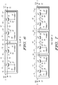
- FIGS. 6-7 are simplified schematic diagrams illustrating internal components of ESD clamps 51, 61 according to further embodiments of the present invention, wherein it will be understood that clamps 51, 61 are substituted for clamp 11 in generalized ESD protection circuit 10 of FIG. 1 .
- ESD clamp 51 differs from ESD clamp 41 of FIG. 5 in that it comprises two serially coupled ESD stages, that is, lower ESD stage or clamp 41 (e.g., clamp 41 of FIG. 5 ) and upper ESD stage or clamp 41' (also analogous to clamp 41 of FIG. 5 ).
- ESD clamp 61 differs from ESD clamp 51 of FIG.
- serially coupled ESD stages that is, lower ESD stage or clamp 41, intermediate ESD stage or clamp 41' and upper or end ESD stage or clamp 41".
- the terms “lower” or “first” and “upper” or “end” or “last” are used herein merely to indicate that one of the serially coupled ESD stages (e.g., “lower or “first” ESD clamp 41) is coupled to so-called GND terminal 23 of ESD circuit 10 and another of the serially coupled ESD stages (e.g., "upper” or “end” or “last” clamp 41' or 41") is coupled to so-called I/O terminals 22 of ESD circuit 10 of FIG.
- Intermediate and upper ESD stages or clamps 41' and 41" are analogous to lower ESD stage or clamp 41 and the convention is adopted of identifying the individual components thereof analogous to those of lower ESD stage or clamp 41 by adding a prime to the individual reference numbers of intermediate stage or clamp 41' and a double prime to the individual reference numbers of upper or end or last stage or clamp 41", for example, emitters 26', 26" of intermediate and upper ESD stages or clamps 41', 41” are analogous to emitter 26 of lower ESD stage or clamp 41, collectors 27', 27" to collector 27, and so forth.
- ESD stages or clamps 41, 41', 41" are coupled so that: (i) node 42 of lower or first stage or clamp 41 is coupled to node 32' of intermediate stage or clamp 41' via node 65; (ii) node 42' of intermediate stage or clamp 41' is coupled to node 32" of end or upper or last stage or clamp 41" via node 65'; (iii) lower or bottom node 32 of lower or first stage of ESD clamp 41 is adapted to be coupled to GND terminal 23 of ESD circuit 10; (iv) top or upper node 42" of upper or end or last stage of ESD clamp 41" is adapted to be coupled to I/O terminals 22 of ESD circuit 10.
- stage or clamp 41" When only two stages are used, then stage or clamp 41" is omitted, and upper node 42' of stage or clamp 41' is coupled to I/O terminals 22.
- ESD clamp 51 of FIG. 6 and ESD clamp 61 of FIG. 7 are referred to as "stacked" or “cascaded” ESD clamps, in that they comprise an electrically serially coupled arrangement of individual bi-directional ESD stages or clamps 41, 41', 41", etc..
- FIG. 6 shows two-stack ESD clamp 51 and FIG. 7 , shows three-stack ESD clamp 61.
- Intermediate nodes 42, 65 and 32 between ESD stacks or clamps 41 and 41', and intermediate nodes 42', 65' and 32" between ESD stacks or clamps 41' and 41" are shown as separate nodes merely for convenience of description and can be combined.
- Such a multiple "stacked" arrangement makes it possible to obtain higher trigger voltage and holding voltage (e.g., voltages Vt1 and Vh of FIG. 3 ) than are generally possible with a single ESD protection stage, such as is illustrated in FIG. 5 .
- the "first" of the N serially coupled ESD stages would ordinarily have its lower node 32 1 (by analogy to stage 41) coupled to GND terminal 23 of circuit 10 of FIG. 1 and the Nth stage would ordinarily have its upper node 42 N (by analogy to stage 41") coupled to the I/O terminals of the circuit core 24 of FIG. 10 , where the subscripts 1, 2, ...N indicate the particular stage.
- the lower, intermediate and upper nodes of the i th ESD stage would be identified as 32 i , 52 i , and 42 i respectively, and the intermediate nodes between electrically adjacent ESD stages "i" and the "(i+1)" would be identified as 65 i .
- FIG. 8 shows simplified schematic cross-sectional view 70 through ESD clamp 71 analogous to ESD clamp 41 of FIG. 5 showing an arrangement of its internal regions and providing further detail.
- ESD clamp 71 comprises P-type substrate (P-SUBSTRATE) 72, N-type buried layer (NBL) 73 and N doped regions 741, 742, 743 (collectively 74).
- N-type buried layer 73 and N doped regions 74 serve as the collectors 27, 37 coupled by node 52 corresponding to N doped region 742.
- ESD clamp 71 further comprises P-type epi regions (P-EPI) 751, 752 (collectively 75) separated by N doped region 742 and P-type diffused regions (P-DIFF) 761, 762 (collectively 76) respectively in P-type epi regions 751, 752 that serve as base regions 28, 38.
- P+ base contact regions 771, 772 are provided in diffused regions 76 wherein base contact region 771 is coupled to base node 34 and base contact region 772 is coupled to base node 44 (see also plan view 84 of FIG. 9 ).
- N+ emitter regions 781, 782 are also provided in diffused regions 76, wherein emitter region 781 is coupled to emitter node 32 and emitter region 782 is coupled to emitter node 42 (see also plan view 84 of FIG. 9 ).
- Resistors 29, 39 couple emitter node 32 to base node 34 and emitter node 42 to base node 44, respectively.
- Resistors 29, 39 are external resistors, that is, fabricated during the same manufacturing process and by the same general techniques used for preparing the core circuit and ESD protection device, but which are not formed within semiconductor 80.
- Conventional surface dielectric passivation layer 79 is also provided.
- FIG. 9 shows simplified schematic plan view 84 of the ESD clamp 71 of FIG. 8 .
- N doped region 74 conveniently has a square plan view shape wherein N doped region 741 forms a central divider or partition, separating P-epi regions 751, 752.
- N doped region 741 corresponds to node 52 of the circuit of FIG. 5 .
- P-diffused regions 761, 762 are located in P-epi regions 751, 752 respectively.
- N+ emitter regions 781, 782 and P+ base contact regions 771, 772 are located in P-diffused regions 761, 762 respectively.
- Emitter region 781 has emitter contact region 783 to which is coupled conductor 81, corresponding to node 32.
- Emitter region 782 has emitter contact region 784, to which is coupled conductor 82 corresponding to node 42.
- Conductors 81, 82 are desirably a highly conductive material such as a metal or heavily doped semiconductor or semi-metal so as to minimize the series resistance of the ESD clamp to the ESD transient.
- P+ base contact regions 771, 772 have ohmic contact regions 773, 774 coupled respectively to conductors 341, 441 which extend to resistors 29, 39 respectively.
- Resistors 29, 39 are thin film resistors, as for example, and not intended to be limiting of poly-silicon or other poly-semiconductor (poly-SC), formed on the upper surface of dielectric passivation layer 79.
- each of resistors 29, 39 is formed from the parallel combination of two resistors 291, 292 and 391, 392, each having a resistance value of 2R, where R is the desired emitter-base coupling resistance value.
- contact nodes 34 on 2R resistances 291, 292 are coupled to base contacts 773 via conductors 341 and to emitter contact 783 via contacts 321 and emitter conductor 81, so that resistances 291, 292 of value 2R are electrically in parallel, thereby yielding the desired resistance value of R.
- contact nodes 44 on 2R resistances 391, 292 are coupled to base contacts 774 via conductors 441 and to emitter contact 784 via contacts 421 and emitter conductor 82, so that resistances 391, 392 of value 2R are electrically in parallel, thereby yielding the desired resistance value of R.
- FIG. 9 shows the resistors R of the circuit of FIG. 5 being provided by a parallel combination of two resistances each of value 2R, persons of skill in the art will understand that this is by way of example and not intended to be limiting.
- Resistances 29, 39 of value R may be provided by a parallel combination of resistors of value 2R, 4R, 6R, etc., or a series combination of resistors of value R/2, R/3, R/4 etc., or by a series-parallel combination of individual resistances of other sizes, or by forming resistances R from one or more strips of resistive material of known resistance per square, and then locating, for example, contacts 321, 421 at different distances along the resistive strip to produce the desired resistances R.
- These modifications can be accomplished merely by altering only the metal contact mask rather than altering multiple masks of the planar process used for forming such ESD clamps.
- the trigger voltage Vt1 can be changed by changing the values of resistance R of resistors 29, 39 of FIG. 5 .
- the invented arrangement of incorporating resistances whose values can be altered by a minimal mask change allows a single process and basic mask set to be easily adapted to provide different desired values of Vt1. This is a significant advantage.
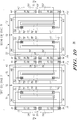
- FIG. 10 is a simplified plan view 94 of two ESD clamps 84, 84' of the type shown in FIG. 9 electrically cascaded or stacked in series to provide ESD clamp 86 analogous to ESD clamp 51 of FIG. 6 comprising stages 41, 41'.
- the same reference numbers are used in FIG. 10 as in FIG. 9 to identify similar elements, wherein the elements of lower or first ESD stage 71, 84 are the same as in FIG. 9 , and those of upper or end or last ESD stage 71', 84' are identified by adding a (') to the corresponding elements. Accordingly, the discussion of FIG. 9 is incorporated herein by reference as applied to FIG. 10 .
- Conductor 81 is adapted to be coupled to GND terminal 23 of circuit 10 of FIG. 1 and conductor 82' is adapted to be coupled to I/O terminal 22 of circuit 10 of FIG. 1 .
- FIGS. 11-12 are plots of current I in amps verses voltage V in volts for ESD clamps according to several embodiments of the invention when subjected to simulated ESD transients obtained from a charged transmission line, for example, as are routinely used for human body model (HBM) testing of ESD clamps.
- FIG. 11 shows I-V plot 90 for single, double and triple stack or stage ESD clamps.
- Trace 91 shows the I-V plot obtained for single stage ESD clamp 41 of FIG. 5 having the cross-section and plan view layout illustrated in FIGS. 8 and 9 , respectively.
- Trace 92 shows the I-V plot obtained for double stack or stage ESD clamp 51 of FIG. 6 having the plan view layout illustrated in FIG.
- Trace 93 shows the I-V plot obtained for triple stack or stage ESD clamp 61 of FIG. 5 having the cross-section and plan view layout corresponding to three serially coupled arrangements of ESD clamps 71 illustrated in FIGS. 8 and 9 , respectively.
- Vt1 for the single stack was 23.7 volts
- Vt1 for the double stack was 48.9 volts
- Vt1 for the triple stack was 73.9 volts, illustrating how different values of trigger voltage Vt1 (and holding voltages) may be obtained by electrically stacking ESD stages.
- the individual ESD stages in the two stack and three stack arrangements were substantially identical to the single stack arrangement and had the same resistance values R 29 , R 39 but this is not essential. It may be desirable in some situations to have resistors R 29 , R 29' , R 29" , etc., have the same resistance values and resistors R 39 , R 39' , R 39" , etc., have different resistance values.
- the device of trace 96 was oriented at 0 or 180 degrees and the device of trace 97 was oriented at 90 or 270 degrees. Stated another way, the devices of traces 96 and 97 were oriented at right angles to each other.
- each bipolar transistor has an emitter, a base and a collector, and wherein the emitter of the second transistor of the first stage is coupled to the emitter of the first transistor of the second stage.
- the first and second resistors have values in the range of about 0.5 k Ohm to 150 K Ohms.
- the first resistors of each of the one or more serially arranged resistor triggered bi-directional ESD clamp stages have substantially the same first values and the second resistors of each of the one or more serially arranged resistor triggered ESD clamp stages have substantially the same second values.
- the first and second resistors have different values.
- the first and second resistors of at least some of the one or more serially arranged resistor triggered bi-directional ESD clamp stages have different values.
- an integrated ESD protection device having I/O and common terminals adapted to be coupled to I/O and common terminals of a core circuit being protected by the integrated ESD protection device, comprising, first and second bipolar transistors having a common collector region and comprising, first and second base regions of a first conductivity type, one base region for each bipolar transistor, a region of a second, opposite conductivity type extending beneath the first and second base regions, and separating and laterally surrounding the first and second base regions, and serving as the common collector region of the first and second bipolar transistors, a first emitter region of the second conductivity type within the first base region and a second emitter region of the second conductivity type within the second base region, wherein the first emitter region is adapted to be coupled to the common terminal of the core circuit and the second emitter region is adapted to be coupled to the I/O terminals of the core circuit, and first and second resistors coupled respectively between the emitter region and the base region of the first transistor and the emitter region and the base region of the
- the first and second resistors are thin film resistors.
- the thin film resistors may be formed of poly-semiconductor. Both the first and second resistors each comprise multiple segments coupled in a series arrangement or a parallel arrangement or a series-parallel arrangement to provide the desired resistance values. According to a still yet further embodiment, the first and second resistors have substantially the same resistance value. According to a yet still further embodiment, the first and second resistors have different resistance values.
- the combination of the first and second transistors and the first and second resistors form a modular ESD clamp stage; and the integrated ESD protection device further comprises two or more serially coupled modular ESD clamp stages.
- an ESD protection device adapted to be coupled between common and I/O terminals of a core circuit desired to be protected, comprising, one or more bi-directional resistor triggered ESD stages, each stage comprising, two bipolar transistors having a common collector and isolation region, a base region for each transistor separated by a portion of the common collector and isolation region, separate emitter regions, one in each base region, base contact regions, one for each base region, and ESD trigger resistors external to the transistors, coupled between the emitter region and the base contact region of each transistor.
- the ESD trigger resistors lie laterally outside the collector and isolation region.
- the ESD trigger resistors are thin film resistors.
- the ESD trigger resistors have resistance values in the range of about 0.5 k Ohms to 150 k Ohms.
Landscapes
- Semiconductor Integrated Circuits (AREA)
- Bipolar Integrated Circuits (AREA)
Description
- The present invention generally relates to electrostatic discharge (ESD) protection of electronic elements and, more particularly, ESD protection of semiconductor components and integrated circuits.
- Modem electronic devices, especially semiconductor (SC) devices and integrated circuits (ICs) are at risk of damage due to electrostatic discharge (ESD) events. It is well known that electrostatic discharge from handling SC devices and ICs, by humans or machines or both, is a source of such excess voltage. Accordingly, it is commonplace to provide an ESD clamp (voltage limiting device) across the input/output (I/O) and other terminals of such SC devices and IC's.
FIG. 1 is a simplified schematic diagram ofcircuit 10 whereinESD clamp 11 is placed between input/output (I/O)terminals 22 and ground orcommon terminal 23 of a SC device or IC to protect the other devices on the chip, that is, to protectcircuit core 24 which is also coupled to I/O terminals 22 aInd common (e.g., "GND")terminal 23. Zener diode symbol 11' withinESD clamp 11 indicates that the function ofESD clamp 11 is to limit the voltage than can appear acrosscircuit core 24 irrespective of the voltage applied to external I/O andGND terminals -
FIG. 2 is a simplified schematic diagram illustrating internal components of priorart ESD clamp 21 which is inserted incircuit 10 in place ofESD clamp 11.ESD clamp 21 comprisesbipolar transistor 25, havingemitter 26,collector 27 andbase 28,resistance 19 and Zener diode 13 havingterminals Resistance 19 can include any inherent contact resistance and the effect of the inherent base resistance (not shown). In applications employing Zener diode 13 it is common to directly connect the base and emitter contacts, in whichcase resistance 19 is small. The purpose ofresistance 19 inESD clamp 21 is not to provide triggering, since this is provided by Zener diode 13 but to keepbase 28 andemitter 26 at substantially the same potential unless there is an ESD event, so that in normal operation ofcircuit 10,ESD clamp 21 does not interfere with the operation ofcircuit core 24. When the voltage acrossterminals bipolar transistor 25 into conduction and desirably clamping the voltage acrossterminals damaging circuit core 24. -
FIG. 3 is a simplified schematic diagram illustrating internal components of priorart ESD clamp 31 which is inserted incircuit 10 in place ofESD clamp 11.ESD clamp 31 comprisesbipolar transistor 25, havingemitter 26,collector 27 andbase 28 andresistor 29.Resistor 29 is generally much larger than the inherent base and contact resistance.Resistor 29 is used to triggerbipolar transistor 25 into conduction when an ESD event occurs. When an ESD event arrives acrossterminals resistor 29. By using a value forresistor 29 that is large compared to the inherent base resistance, sufficient voltage is developed acrossresistor 29 to bias the emitter-base junction into conduction, thereby turning ontransistor 25 and providing ESD protection by clamping the external voltage at a level below that capable of causing damage tocircuit core 24. After the ESD transient has passed,resistor 29 discharges any charge stored on the emitter base junction, thereby returningtransistor 25 to its non-conductive state so that in normal operation ofcircuit 10,ESD clamp 21 does not interfere with the operation ofcircuit core 24. - Design, construction and operation of such ESD devices is described for example in commonly owned United States Patent
7,164,566 B2 "Electrostatic Discharge Protection Device and Method Therefore" by Hongzhong Xu et al, and further described by Danielle Coffing and Richard Ida in "Analysis of a Zener-Triggered Bipolar ESD Structure in a BiCMOS Technology", IEEE BCTM 1998, pages 31-34, and by Joshi, Ida, Givelin and Rosenbaum in "An Analysis of Bipolar Breakdown and its Application to the Design of ESD Protection Circuits", IEEE 01CH37167, 39th Annual International Reliability Physics Symposium, Orlando, FL, 2001, pages 240-245.FIG. 4 is an illustration of a typical current-voltage characteristic of an ESD clamp, where voltage Vt1 is referred to as the trigger voltage and voltage Vh is referred to as the holding voltage.US-A1-2007/0008667 describes a silicon controlled rectifier, with a constant negative current to ensure cutoff at most times.US-B1-7 196 361 shows a pair of parallel connected circuits, which provide a 'tuneable' SCR.US-B1-6 236 087 shows a pair of cascaded DIACS. - The present invention will hereinafter be described in conjunction with the following drawing figures, wherein like numerals denote like elements, and wherein:
-
FIG. 1 is a simplified schematic diagram of a generalized ESD protection circuit using an ESD clamp to protect a circuit core from electrostatic discharge (ESD) events; -
FIG. 2 is a simplified schematic diagram illustrating internal components of a prior art ESD clamp; -
FIG. 3 is a simplified schematic diagram illustrating internal components of a further prior art ESD clamp; -
FIG. 4 is an illustration of a typical current-voltage characteristic of the ESD clamp ofFIGS. 2 and 3 ; -
FIG. 5 is a simplified schematic diagram illustrating internal components of an ESD clamp according to an embodiment of the present invention; -
FIGS. 6-7 are simplified schematic diagram illustrating internal components of ESD clamp according to further embodiments of the present invention in which, inFIG.6 , two ESD clamps of the type shown inFIG. 5 have been electrically cascaded or stacked and inFIG. 7 , three ESD stages of the type shown inFIG. 5 have been electrically cascaded or stacked, in order to achieve higher and higher trigger voltage; -
FIG. 8 is a simplified schematic cross-sectional view through the ESD clamp ofFIG. 5 showing an arrangement of its internal regions according to an embodiment of the present invention and providing further detail; -
FIG. 9 is a simplified schematic plan view of the ESD clamp ofFIG. 8 ; -
FIG. 10 is a simplified plan view of two ESD clamps of the type shown inFIG. 9 electrically cascaded or stacked according to the circuit ofFIG. 6 ; -
FIGS. 11-12 are plots of current verses voltage for ESD clamps according to several embodiments of the invention, illustrating how the trigger voltage Vt1 may be adjusted by changing values of R and/or by electrically cascading or stacking modular ESD stages. - The following detailed description is merely exemplary in nature and is not intended to limit the invention or the application and uses of the invention. Furthermore, there is no intention to be bound by any expressed or implied theory presented in the preceding technical field, background, or the following detailed description.
- For simplicity and clarity of illustration, the drawing figures illustrate the general manner of construction, and descriptions and details of well-known features and techniques may be omitted to avoid unnecessarily obscuring the invention. Additionally, elements in the drawings figures are not necessarily drawn to scale. For example, the dimensions of some of the elements or regions in the figures may be exaggerated relative to other elements or regions to help improve understanding of embodiments of the invention.
- The terms "first," "second," "third," "fourth" and the like in the description and the claims, if any, may be used for distinguishing between similar elements and not necessarily for describing a particular sequential or chronological order. It is to be understood that the terms so used are interchangeable under appropriate circumstances such that the embodiments of the invention described herein are, for example, capable of operation in sequences other than those illustrated or otherwise described herein. Furthermore, the terms "comprise," "include," "have" and any variations thereof, are intended to cover non-exclusive inclusions, such that a process, method, article, or apparatus that comprises a list of elements is not necessarily limited to those elements, but may include other elements not expressly listed or inherent to such process, method, article, or apparatus. The term "coupled," as used herein, is defined as directly or indirectly connected in an electrical or non-electrical manner.
- While the circuits of
FIGS. 2 and 3 can be effective in providing ESD protection, further improvements are desirable. Accordingly, there is an ongoing need to provide improved ESD clamps, especially ESD clamps that are adapted to achieve a variety of predetermined trigger voltages, and that are bidirectional so as to conserve chip area, and that are modular in nature so as to electrically stackable, and that are less sensitive to manufacturing variations that can adversely affect manufacturing yield. Other desirable features and characteristics of the present invention will become apparent from the subsequent detailed description of the invention and the appended claims, taken in conjunction with the accompanying drawings and this background of the invention. -
FIG. 5 is a simplified schematic diagram illustrating internal components ofESD clamp 41, according to an embodiment of the present invention.ESD clamp 41 is used ingeneralized protection circuit 10 in place ofESD clamp 11.ESD clamp 41 differs from priorart ESD clamps FIGS. 2 and 3 in that it utilizes two mirror coupled transistor stages T1 and T2 joined atnode 52 and further does not have Zener diode 13. Transistor stage T1 comprisestransistor 25 analogous totransistor 25 ofFIGS. 2-3 withemitter 26,collector 27 andbase 28, plusresistor 29, coupled in generally the same manner as inFIGS. 2 and 3 . The same reference numbers are used for transistor stage T1 andESD clamp 31 ofFIG. 3 , to indicate that the individual elements are analogous but not necessarily identical.Resistor 29 is coupled betweenbase 28 atnode 34 andemitter 26 atnode 32.Node 32 is adapted to be coupled toGND terminal 23 ofESD protection circuit 10 ofFIG. 1 . Transistor stage T2 comprisestransistor 35 havingemitter 36,collector 37 andbase 38.Resistor 39 is coupled betweenbase 38 atnode 44 andemitter 36 atnode 42.Node 43 of Transistor stage T2 is coupled tonode 33 of transistor stage T1 vianode 52.Nodes Node 42 of Transistor stage T2 is adapted to be coupled to input/output (I/O)terminals 22 ofESD circuit 10 ofFIG. 1 . It will be noted that while stages T1 and T2 ofESD clamp 41 individually resembleESD clamp 31 ofFIG. 3 , they are serially coupled in opposition or in mirror arrangement, that is,node 43 of transistor stage T2 is coupled tonode 33 of transistor stage T1, or to say it another way,collector 27 of transistor stage T1 is coupled tocollector 37 of transistor stage T2 viacommon node 52. An advantage ofESD clamp 41 compared to ESD clamps 21 and 31 is thatESD clamp 41 is bi-directional, that is, it will respond, for example, to a positive going ESD transient at either ofterminals ESD circuit 10. This is a significant advantage since it results in a substantial area saving in providing bi-directional ESD protection tocircuit core 24, and thereby lowers the cost of manufacture of the SC device or IC containingcircuit core 24 ofFIG. 1 . -
FIGS. 6-7 are simplified schematic diagrams illustrating internal components of ESD clamps 51, 61 according to further embodiments of the present invention, wherein it will be understood that clamps 51, 61 are substituted forclamp 11 in generalizedESD protection circuit 10 ofFIG. 1 .ESD clamp 51 differs fromESD clamp 41 ofFIG. 5 in that it comprises two serially coupled ESD stages, that is, lower ESD stage or clamp 41 (e.g., clamp 41 ofFIG. 5 ) and upper ESD stage or clamp 41' (also analogous to clamp 41 ofFIG. 5 ).ESD clamp 61 differs fromESD clamp 51 ofFIG. 6 in that it comprises three serially coupled ESD stages, that is, lower ESD stage or clamp 41, intermediate ESD stage or clamp 41' and upper or end ESD stage or clamp 41". The terms "lower" or "first" and "upper" or "end" or "last" are used herein merely to indicate that one of the serially coupled ESD stages (e.g., "lower or "first" ESD clamp 41) is coupled to so-calledGND terminal 23 ofESD circuit 10 and another of the serially coupled ESD stages (e.g., "upper" or "end" or "last"clamp 41' or 41") is coupled to so-called I/O terminals 22 ofESD circuit 10 ofFIG. 1 , wherein GND is usually (but not always) the lower potential side ofcircuit 10 and the I/O terminals are coupled to what is usually (but not always) the higher potential side ofESD circuit 10. The designations of "lower" or "first" and "upper" or "end" or "last" are merely for convenience of reference and not intended to be limiting. Lower ESD stage or clamp 41 is described in connection withFIG. 5 . Intermediate and upper ESD stages or clamps 41' and 41" are analogous to lower ESD stage or clamp 41 and the convention is adopted of identifying the individual components thereof analogous to those of lower ESD stage or clamp 41 by adding a prime to the individual reference numbers of intermediate stage or clamp 41' and a double prime to the individual reference numbers of upper or end or last stage or clamp 41", for example,emitters 26', 26" of intermediate and upper ESD stages or clamps 41', 41" are analogous to emitter 26 of lower ESD stage or clamp 41,collectors 27', 27" tocollector 27, and so forth. ESD stages or clamps 41, 41', 41" are coupled so that: (i)node 42 of lower or first stage or clamp 41 is coupled to node 32' of intermediate stage or clamp 41' vianode 65; (ii) node 42' of intermediate stage or clamp 41' is coupled tonode 32" of end or upper or last stage or clamp 41" via node 65'; (iii) lower orbottom node 32 of lower or first stage ofESD clamp 41 is adapted to be coupled toGND terminal 23 ofESD circuit 10; (iv) top orupper node 42" of upper or end or last stage ofESD clamp 41" is adapted to be coupled to I/O terminals 22 ofESD circuit 10. When only two stages are used, then stage or clamp 41" is omitted, and upper node 42' of stage or clamp 41' is coupled to I/O terminals 22.ESD clamp 51 ofFIG. 6 and ESD clamp 61 ofFIG. 7 are referred to as "stacked" or "cascaded" ESD clamps, in that they comprise an electrically serially coupled arrangement of individual bi-directional ESD stages or clamps 41, 41', 41", etc..FIG. 6 shows two-stack ESD clamp 51 andFIG. 7 , shows three-stack ESD clamp 61.Intermediate nodes intermediate nodes 42', 65' and 32" between ESD stacks or clamps 41' and 41" are shown as separate nodes merely for convenience of description and can be combined. Such a multiple "stacked" arrangement makes it possible to obtain higher trigger voltage and holding voltage (e.g., voltages Vt1 and Vh ofFIG. 3 ) than are generally possible with a single ESD protection stage, such as is illustrated inFIG. 5 . - While
FIGS. 6 and 7 illustrate two-stack and three-stack configurations, respectively, any number N of ESD stages 41, where N = 1, 2, 3, 4, ... etc., may be stacked in generally the same manner and the "N-stack" substituted forESD clamp 11 ofFIG. 1 . In such case, then the "first" of the N serially coupled ESD stages would ordinarily have its lower node 321 (by analogy to stage 41) coupled toGND terminal 23 ofcircuit 10 ofFIG. 1 and the Nth stage would ordinarily have its upper node 42N (by analogy to stage 41") coupled to the I/O terminals of thecircuit core 24 ofFIG. 10 , where thesubscripts 1, 2, ...N indicate the particular stage. In the same manner, the lower, intermediate and upper nodes of the ith ESD stage would be identified as 32i, 52i, and 42i respectively, and the intermediate nodes between electrically adjacent ESD stages "i" and the "(i+1)" would be identified as 65i. -
FIG. 8 shows simplified schematiccross-sectional view 70 throughESD clamp 71 analogous toESD clamp 41 ofFIG. 5 showing an arrangement of its internal regions and providing further detail. For convenience of reference to the circuit schematic ofESD clamp 41 ofFIG. 5 , the corresponding physical regions ofESD clamp 71 are identified with the corresponding reference numbers used inFIG. 5 . Referring now to bothFIGS. 5 and8 ,ESD clamp 71 comprises P-type substrate (P-SUBSTRATE) 72, N-type buried layer (NBL) 73 and N dopedregions layer 73 and N dopedregions 74 serve as thecollectors node 52 corresponding to N dopedregion 742.ESD clamp 71 further comprises P-type epi regions (P-EPI) 751, 752 (collectively 75) separated by N dopedregion 742 and P-type diffused regions (P-DIFF) 761, 762 (collectively 76) respectively in P-type epi regions base regions base contact regions 771, 772 (collectively 77) are provided in diffusedregions 76 whereinbase contact region 771 is coupled tobase node 34 andbase contact region 772 is coupled to base node 44 (see also planview 84 ofFIG. 9 ).N+ emitter regions 781, 782 (collectively 78) are also provided in diffusedregions 76, whereinemitter region 781 is coupled toemitter node 32 andemitter region 782 is coupled to emitter node 42 (see also planview 84 ofFIG. 9 ).Resistors couple emitter node 32 tobase node 34 andemitter node 42 tobase node 44, respectively.Resistors semiconductor 80. Conventional surfacedielectric passivation layer 79 is also provided. -
FIG. 9 shows simplifiedschematic plan view 84 of theESD clamp 71 ofFIG. 8 . Like reference numbers are used inFIGS. 8 and 9 to refer to like regions. N dopedregion 74 conveniently has a square plan view shape wherein N dopedregion 741 forms a central divider or partition, separating P-epiregions region 741 corresponds tonode 52 of the circuit ofFIG. 5 . P-diffusedregions regions N+ emitter regions base contact regions regions Emitter region 781 hasemitter contact region 783 to which is coupledconductor 81, corresponding tonode 32.Emitter region 782 hasemitter contact region 784, to which is coupled conductor 82 corresponding tonode 42.Conductors 81, 82 are desirably a highly conductive material such as a metal or heavily doped semiconductor or semi-metal so as to minimize the series resistance of the ESD clamp to the ESD transient. P+base contact regions ohmic contact regions conductors resistors Resistors dielectric passivation layer 79. In this embodiment, each ofresistors resistors contact nodes 34 on2R resistances base contacts 773 viaconductors 341 and to emitter contact 783 viacontacts 321 andemitter conductor 81, so thatresistances value 2R are electrically in parallel, thereby yielding the desired resistance value of R. Similarly,contact nodes 44 on2R resistances base contacts 774 viaconductors 441 and to emitter contact 784 viacontacts 421 and emitter conductor 82, so thatresistances value 2R are electrically in parallel, thereby yielding the desired resistance value of R. While the embodiment ofFIG. 9 shows the resistors R of the circuit ofFIG. 5 being provided by a parallel combination of two resistances each ofvalue 2R, persons of skill in the art will understand that this is by way of example and not intended to be limiting.Resistances value 2R, 4R, 6R, etc., or a series combination of resistors of value R/2, R/3, R/4 etc., or by a series-parallel combination of individual resistances of other sizes, or by forming resistances R from one or more strips of resistive material of known resistance per square, and then locating, for example,contacts resistors FIG. 5 . Thus, the invented arrangement of incorporating resistances whose values can be altered by a minimal mask change allows a single process and basic mask set to be easily adapted to provide different desired values of Vt1. This is a significant advantage. -
FIG. 10 is asimplified plan view 94 of two ESD clamps 84, 84' of the type shown inFIG. 9 electrically cascaded or stacked in series to provide ESD clamp 86 analogous toESD clamp 51 ofFIG. 6 comprisingstages 41, 41'. The same reference numbers are used inFIG. 10 as inFIG. 9 to identify similar elements, wherein the elements of lower orfirst ESD stage FIG. 9 , and those of upper or end or last ESD stage 71', 84' are identified by adding a (') to the corresponding elements. Accordingly, the discussion ofFIG. 9 is incorporated herein by reference as applied toFIG. 10 .Conductor 81 is adapted to be coupled toGND terminal 23 ofcircuit 10 ofFIG. 1 and conductor 82' is adapted to be coupled to I/O terminal 22 ofcircuit 10 ofFIG. 1 . - It has been found that the arrangement illustrated in
FIGS. 5-7 and8-10 provide very useful ESD protection when applied incircuit 10 ofFIG. 1 , and that the values of Vt1 can be easily adjusted to suit different circumstances, e.g., different circuit operating voltages and/or desired protection thresholds. The entries in Table I show how varying the value of resistances R in the various embodiments can be used to adjust the desired trigger voltage Vt1. The data of Table I was taken on ESD devices corresponding to the circuit shown inFIG. 5 and the physical implementation illustrated inFIGS. 8-9 , where R29 and R39 are the values ofresistors Table I - Single Stack, Bi-directional. Resistor Triggered ESD device R29 = R39 = 2 kΩ R29 = R39 = 4 kΩ R29 = R39 = 8 kΩ R29 = R39 = 20 kΩ Vt1 = 44.41 volts Vt1 = 32.9 volts Vt1 = 27.44 volts Vt1 = 23.5 volts -
FIGS. 11-12 are plots of current I in amps verses voltage V in volts for ESD clamps according to several embodiments of the invention when subjected to simulated ESD transients obtained from a charged transmission line, for example, as are routinely used for human body model (HBM) testing of ESD clamps.FIG. 11 showsI-V plot 90 for single, double and triple stack or stage ESD clamps.Trace 91 shows the I-V plot obtained for singlestage ESD clamp 41 ofFIG. 5 having the cross-section and plan view layout illustrated inFIGS. 8 and 9 , respectively.Trace 92 shows the I-V plot obtained for double stack or stageESD clamp 51 ofFIG. 6 having the plan view layout illustrated inFIG. 10 and cross-sectional views corresponding to two serially coupled arrangements of the cross-section shown inFIG. 8 .Trace 93 shows the I-V plot obtained for triple stack or stageESD clamp 61 ofFIG. 5 having the cross-section and plan view layout corresponding to three serially coupled arrangements of ESD clamps 71 illustrated inFIGS. 8 and 9 , respectively. In all three cases the resistor values R29, R39 were set at 40 k Ohms, that is R29 = R39 = R29'= R39' = R29" = R39" = 40 k Ohms. Vt1 for the single stack (trace 91) was 23.7 volts, Vt1 for the double stack (trace 92) was 48.9 volts, and Vt1 for the triple stack (trace 93) was 73.9 volts, illustrating how different values of trigger voltage Vt1 (and holding voltages) may be obtained by electrically stacking ESD stages. For experimental convenience, the individual ESD stages in the two stack and three stack arrangements were substantially identical to the single stack arrangement and had the same resistance values R29, R39 but this is not essential. It may be desirable in some situations to have resistors R29, R29', R29", etc., have the same resistance values and resistors R39, R39', R39", etc., have different resistance values. -
FIG. 12 showsI-V plot 95 for a double stack or stage ESD clamp corresponding to the circuit ofESD clamp 51 ofFIG. 6 and cross-section and plan layout shown inFIGS. 8-9 respectively, with R29, R39 = 40 k Ohms but oriented in different directions on the same wafer. The device oftrace 96 was oriented at 0 or 180 degrees and the device oftrace 97 was oriented at 90 or 270 degrees. Stated another way, the devices oftraces trace 97 gave Vt1 = 53.1 volts. This is an important result since it is well known in the art that ESD clamps often are orientation sensitive, that is, nominally identical ESD clamps on the same wafer or die, but with different azimuthal orientations in plan view can exhibit significantly different values of Vt1 and I-V behavior, to the detriment of performance and manufacturing yield. The fact illustrated inFIG. 12 that the invented arrangement does not exhibit this behavior is a significant and economically important result. - The two-stack results (trace 92) of
FIG. 11 with 40k Ohm resistors gave Vt1 = 48.9 and the two stack results ofFIG. 12 (traces 96, 97) gave Vt1 = 53.4 and 53.1. The difference in Vt1 results = (53.25-48.9)/48.9 = 8.8% occurred because the devices ofFIG. 12 where of smaller area than those ofFIG. 11 . While Vt1 depends strongly on the value of resistors R29 R39, etc., as shown by Table I, Vt1 is also weakly dependent on the device size, thereby providing another means for fine tuning the desired value of Vt1. - According to an embodiment, there are two or more resistor triggered bi-directional ESD clamp stages and each bipolar transistor has an emitter, a base and a collector, and wherein the emitter of the second transistor of the first stage is coupled to the emitter of the first transistor of the second stage. According to a still yet further embodiment, there are three or more resistor triggered bi-directional ESD clamp stages and each bipolar transistor has an emitter, a base and a collector, and wherein the emitter of the second transistor of the first stage is coupled to the emitter of the first transistor of the second stage and the emitter of the second transistor of the second stage is coupled to the emitter of the first transistor of the third stage. According to a yet still further embodiment, the first and second resistors have values in the range of about 0.5 k Ohm to 150 K Ohms. According to another embodiment, the first resistors of each of the one or more serially arranged resistor triggered bi-directional ESD clamp stages have substantially the same first values and the second resistors of each of the one or more serially arranged resistor triggered ESD clamp stages have substantially the same second values. According to a still another embodiment, the first and second resistors have different values. According to a yet another embodiment, the first and second resistors of at least some of the one or more serially arranged resistor triggered bi-directional ESD clamp stages have different values.
- There is provided an integrated ESD protection device, having I/O and common terminals adapted to be coupled to I/O and common terminals of a core circuit being protected by the integrated ESD protection device, comprising, first and second bipolar transistors having a common collector region and comprising, first and second base regions of a first conductivity type, one base region for each bipolar transistor, a region of a second, opposite conductivity type extending beneath the first and second base regions, and separating and laterally surrounding the first and second base regions, and serving as the common collector region of the first and second bipolar transistors, a first emitter region of the second conductivity type within the first base region and a second emitter region of the second conductivity type within the second base region, wherein the first emitter region is adapted to be coupled to the common terminal of the core circuit and the second emitter region is adapted to be coupled to the I/O terminals of the core circuit, and first and second resistors coupled respectively between the emitter region and the base region of the first transistor and the emitter region and the base region of the second transistor, wherein the first and second resistors are located so that portions of the region of second, opposite, conductivity type are located between the first resistor and the first base region and between the second resistor and the second base region. The first and second resistors are thin film resistors. The thin film resistors may be formed of poly-semiconductor. Both the first and second resistors each comprise multiple segments coupled in a series arrangement or a parallel arrangement or a series-parallel arrangement to provide the desired resistance values. According to a still yet further embodiment, the first and second resistors have substantially the same resistance value. According to a yet still further embodiment, the first and second resistors have different resistance values. According to another embodiment, the combination of the first and second transistors and the first and second resistors form a modular ESD clamp stage; and the integrated ESD protection device further comprises two or more serially coupled modular ESD clamp stages.
- According to a further example there is provided an ESD protection device adapted to be coupled between common and I/O terminals of a core circuit desired to be protected, comprising, one or more bi-directional resistor triggered ESD stages, each stage comprising, two bipolar transistors having a common collector and isolation region, a base region for each transistor separated by a portion of the common collector and isolation region, separate emitter regions, one in each base region, base contact regions, one for each base region, and ESD trigger resistors external to the transistors, coupled between the emitter region and the base contact region of each transistor. According to a still further example, the ESD trigger resistors lie laterally outside the collector and isolation region. According to a still further embodiment, the ESD trigger resistors are thin film resistors. According to a yet further example, the ESD trigger resistors have resistance values in the range of about 0.5 k Ohms to 150 k Ohms.
- While at least one exemplary embodiment has been presented in the foregoing detailed description of the invention, it should be appreciated that a vast number of variations exist. It should also be appreciated that the exemplary embodiment or exemplary embodiments are only examples, and are not intended to limit the scope, applicability, or configuration of the invention in any way. Rather, the foregoing detailed description will provide those skilled in the art with a convenient road map for implementing an exemplary embodiment of the invention, it being understood that various changes may be made in the function and arrangement of elements described in an exemplary embodiment without departing from the scope of the invention as set forth in the appended claims.
Claims (10)
- An electronic device (51, 94) having input/output (I/O) (22) and common (23) terminals, comprising:a circuit core (24) coupled between the I/O (22) and common (23) terminals; and characterized by:a plurality of serially arranged resistor triggered bi-directional electrostatic discharge (ESD) clamp stages (71, 71') coupled between the I/O and common terminals,wherein a first electrostatic discharge clamp stage (41, 71) of the plurality of electrostatic discharge clamp stages comprises serially coupled first (25) and second (35) bipolar transistors located in a substrate, a first external resistor (29) coupled between an emitter (26) and a base (28) of the first bipolar transistor, and a second external resistor (39) coupled between an emitter (36) and a base (38) of the second bipolar transistor, wherein the emitter (26) of the first bipolar transistor is coupled to the common terminal (23), and collectors (27, 37) of the first and second bipolar transistors are coupled together,wherein a second electrostatic discharge clamp stage (41', 71') of the plurality of electrostatic discharge clamp stages comprises serially coupled third (25') and fourth (35') bipolar transistors located in said substrate, a third external resistor (29') coupled between an emitter (26') and a base (28') of the third bipolar transistor, and a fourth external resistor (39') coupled between an emitter (36') and a base (38') of the fourth bipolar transistor, wherein the emitter (26') of the third bipolar transistor is coupled to the emitter (36) of the second bipolar transistor, and collectors (27', 37') of the third and fourth bipolar transistors are coupled together,wherein each of said external resistors is a thin film resistor and comprises at least two resistors (291, 292, 391, 392, 291', 292', 391', 392') formed on an upper surface of a dielectric passivation layer (79) located on a surface of said substrate, andwherein the resistors of each said external thin film resistor are connectedin parallel, in series, or in a series-parallel combination to provide an emitter-base coupling resistance value for providing a desired trigger voltage (Vt1) of the ESD clamp stage.
- The device of claim 1, wherein the first (29), second (39), third (29') and fourth (39') external resistors have values in the range of about 0.5 kΩ to 150 KΩ.
- The device of claim 1 or claim 2, wherein:(i) there are three or more resistor triggered bi-directional electrostatic discharge clamp stages (41, 41', 41"); and(ii) the emitter (36') of the fourth transistor (35') of the second electrostatic discharge clamp stage (41') is coupled to an emitter (26") of a fifth transistor (25") of a third electrostatic discharge clamp stage (41").
- The device of claim 1 or claim 2, wherein:(i) the first (29) and third (29') external resistors have substantially the same first values; and(ii) the second (39) and fourth (39') external resistors have substantially the same second values.
- The device of claim 3, wherein:(i) the third electrostatic discharge clamp stage (41") comprises a fifth external resistor (29") coupled between an emitter (26") and a base (28") of the fifth bipolar transistor (25"), and a sixth external resistor (39") coupled between an emitter (36") and a base (38") of a sixth bipolar transistor (35");(ii) the first (29), third (29') and fifth (29") external resistors have substantially the same first values; and(iii) the second (39), fourth (39') and sixth (39") external resistors have substantially the same second values.
- The device of claim 4 or claim 5, wherein the first and second values are different.
- The device of claim 3, wherein:(i) the third electrostatic discharge clamp stage (41") comprises a fifth external resistor (29") coupled between an emitter (26") and a base (28") of the fifth bipolar transistor (25"), and a sixth external resistor (39") coupled between an emitter (36") and a base (38") of a sixth bipolar transistor (35"); and(ii) at least some of the pairs of first (29) and second (39) resistors, and/or third (29') and fourth (39') resistors, and/or fifth (29") and sixth (39") resistors, have different values.
- The device of claim 1, wherein the device has a top surface, and the plurality of electrostatic discharge clamp stages comprises:(i) a substrate (72) of a first conductivity type;(ii) a buried layer (73) of a second and opposite conductivity type, positioned below the top surface;(iii) doped first regions (741, 742, 743) of the second conductivity type extending from the top surface to the buried layer (73), wherein the buried layer and the first doped regions serve as collectors of the first, second, third and fourth bipolar transistors;(iv) epitaxial second regions (751, 752) of the first conductivity type extending from the top surface to the buried layer (73) and separated by the first regions (741, 742, 743);(v) diffused third regions (76, 761, 762) of the first conductivity type extending from the top surface and located within the second regions, wherein the third regions serve as base regions (28, 38) of the first, second, third and fourth bipolar transistors;(vi) base contact regions (77, 771, 772) of the first conductivity type within the third regions (76, 761, 762); and(vii) emitter regions (781, 782) of the second conductivity type within the third regions (76, 761, 762).
- The device of any previous claim, wherein:the contact nodes (44, 34') of the second external resistor (39) and third external resistor (29') are coupled, with a single conductor (82), to the emitter (36, 784) of the second bipolar transistor (35) and the emitter (26', 783') of the third bipolar transistor (25').
- The device of any previous claim, wherein:one or more of the first (29), second (39), third (29') and fourth (39') external resistors comprise a parallel combination of resistors (291, 292; 391, 392; 291', 292'; 391', 392').
Applications Claiming Priority (2)
| Application Number | Priority Date | Filing Date | Title |
|---|---|---|---|
| US12/038,146 US7911750B2 (en) | 2008-02-27 | 2008-02-27 | Resistor triggered electrostatic discharge protection |
| PCT/US2009/031204 WO2009108410A2 (en) | 2008-02-27 | 2009-01-16 | Resistor triggered electrostatic discharge protection |
Publications (3)
| Publication Number | Publication Date |
|---|---|
| EP2248172A2 EP2248172A2 (en) | 2010-11-10 |
| EP2248172A4 EP2248172A4 (en) | 2011-07-20 |
| EP2248172B1 true EP2248172B1 (en) | 2017-08-02 |
Family
ID=40998067
Family Applications (1)
| Application Number | Title | Priority Date | Filing Date |
|---|---|---|---|
| EP09715944.6A Not-in-force EP2248172B1 (en) | 2008-02-27 | 2009-01-16 | Resistor triggered electrostatic discharge protection |
Country Status (4)
| Country | Link |
|---|---|
| US (1) | US7911750B2 (en) |
| EP (1) | EP2248172B1 (en) |
| TW (1) | TW200941706A (en) |
| WO (1) | WO2009108410A2 (en) |
Families Citing this family (29)
| Publication number | Priority date | Publication date | Assignee | Title |
|---|---|---|---|---|
| US8193560B2 (en) * | 2009-06-18 | 2012-06-05 | Freescale Semiconductor, Inc. | Voltage limiting devices |
| US8648419B2 (en) * | 2010-01-20 | 2014-02-11 | Freescale Semiconductor, Inc. | ESD protection device and method |
| US8390092B2 (en) | 2010-11-12 | 2013-03-05 | Freescale Semiconductor, Inc. | Area-efficient high voltage bipolar-based ESD protection targeting narrow design windows |
| US8982516B2 (en) | 2010-11-12 | 2015-03-17 | Freescale Semiconductor, Inc. | Area-efficient high voltage bipolar-based ESD protection targeting narrow design windows |
| US8686470B2 (en) | 2011-01-07 | 2014-04-01 | Nxp, B.V. | ESD protection circuit |
| EP2515334B1 (en) * | 2011-04-20 | 2013-11-20 | Nxp B.V. | ESD protection circuit |
| US20160277017A1 (en) * | 2011-09-13 | 2016-09-22 | Fsp Technology Inc. | Snubber circuit |
| US10522675B2 (en) * | 2012-01-25 | 2019-12-31 | Infineon Technologies Ag | Integrated circuit including field effect transistor structures with gate and field electrodes and methods for manufacturing and operating an integrated circuit |
| US9018673B2 (en) | 2012-08-31 | 2015-04-28 | Freescale Semiconductor Inc. | Zener diode device and fabrication |
| US9019667B2 (en) * | 2012-11-08 | 2015-04-28 | Freescale Semiconductor Inc. | Protection device and related fabrication methods |
| US8921943B2 (en) | 2012-12-10 | 2014-12-30 | Taiwan Semiconductor Manufacturing Company, Ltd. | Methods and apparatus for ESD structures |
| US9129806B2 (en) | 2013-05-22 | 2015-09-08 | Freescale Semiconductor Inc. | Protection device and related fabrication methods |
| US9502890B2 (en) | 2013-05-22 | 2016-11-22 | Freescale Semiconductor, Inc. | Protection device and related fabrication methods |
| US9543420B2 (en) | 2013-07-19 | 2017-01-10 | Nxp Usa, Inc. | Protection device and related fabrication methods |
| US9330961B2 (en) * | 2013-09-23 | 2016-05-03 | Freescale Semiconductor, Inc. | Stacked protection devices and related fabrication methods |
| US9099487B2 (en) | 2013-12-05 | 2015-08-04 | Freescale Semiconductor Inc. | Zener diode devices and related fabrication methods |
| US9287255B2 (en) | 2014-07-09 | 2016-03-15 | Freescale Semiconductor Inc. | ESD protection device and related fabrication methods |
| US9780558B2 (en) | 2014-12-11 | 2017-10-03 | Nxp Usa, Inc. | Semiconductor device and related protection methods |
| CN104600068B (en) * | 2015-01-20 | 2018-06-26 | 湖州迈康电子科技有限公司 | A kind of high-voltage bidirectional ESD protective device based on longitudinal NPN structures |
| US9620496B2 (en) | 2015-03-10 | 2017-04-11 | Nxp Usa, Inc. | Stacked protection devices with overshoot protection and related fabrication methods |
| US10037986B2 (en) * | 2015-03-19 | 2018-07-31 | Nxp Usa, Inc. | ESD protection structure and method of fabrication thereof |
| US9960251B2 (en) | 2015-03-19 | 2018-05-01 | Nxp Usa, Inc. | ESD protection structure and method of fabrication thereof |
| TWI591793B (en) * | 2015-03-26 | 2017-07-11 | 立積電子股份有限公司 | Electrostatic discharge protection circuit |
| US9893050B2 (en) | 2015-06-30 | 2018-02-13 | Nxp Usa, Inc. | ESD protection structure |
| EP3467874B1 (en) | 2017-10-03 | 2020-09-23 | NXP USA, Inc. | Single-stack bipolar-based esd protection device |
| US11069675B2 (en) * | 2018-05-17 | 2021-07-20 | Jiangnan University | ESD protection device with bidirectional diode string-triggering SCR structure |
| US11201466B2 (en) | 2018-07-12 | 2021-12-14 | Globalfoundries U.S. Inc. | Electrostatic discharge clamp structures |
| CN109119417B (en) * | 2018-08-24 | 2021-10-26 | 电子科技大学 | Latch-up immune bidirectional ESD protection device |
| US11532610B2 (en) * | 2020-06-24 | 2022-12-20 | Amazing Microelectronic Corp. | Electrostatic discharge protection structure and electrostatic discharge protection circuit with low parasitic capacitance thereof |
Family Cites Families (16)
| Publication number | Priority date | Publication date | Assignee | Title |
|---|---|---|---|---|
| US5276582A (en) * | 1992-08-12 | 1994-01-04 | National Semiconductor Corporation | ESD protection using npn bipolar transistor |
| US5602409A (en) * | 1995-07-13 | 1997-02-11 | Analog Devices, Inc. | Bidirectional electrical overstress protection circuit for bipolar and bipolar-CMOS integrated circuits |
| JP2850801B2 (en) * | 1995-07-28 | 1999-01-27 | 日本電気株式会社 | Semiconductor element |
| US6365924B1 (en) * | 1998-06-19 | 2002-04-02 | National Semiconductor Corporation | Dual direction over-voltage and over-current IC protection device and its cell structure |
| US6236087B1 (en) * | 1998-11-02 | 2001-05-22 | Analog Devices, Inc. | SCR cell for electrical overstress protection of electronic circuits |
| US20010043449A1 (en) * | 2000-05-15 | 2001-11-22 | Nec Corporation | ESD protection apparatus and method for fabricating the same |
| US6472286B1 (en) * | 2000-08-09 | 2002-10-29 | Taiwan Semiconductor Manufacturing Company | Bipolar ESD protection structure |
| US6483168B1 (en) * | 2001-09-13 | 2002-11-19 | National Semiconductor Corporation | Integrated circuit having resistor formed over emitter of vertical bipolar transistor |
| US6970336B2 (en) | 2003-10-10 | 2005-11-29 | Freescale Semiconductor, Inc. | Electrostatic discharge protection circuit and method of operation |
| US20050083618A1 (en) * | 2003-10-21 | 2005-04-21 | Steinhoff Robert M. | ESD protection for integrated circuits |
| US7196361B1 (en) * | 2003-12-12 | 2007-03-27 | National Semiconductor Corporation | Cascoded bi-directional high voltage ESD protection structure |
| TWI223432B (en) * | 2003-12-18 | 2004-11-01 | Univ Nat Chiao Tung | Double-triggered silicon controller rectifier and relevant circuitry |
| US7164566B2 (en) * | 2004-03-19 | 2007-01-16 | Freescale Semiconductor, Inc. | Electrostatic discharge protection device and method therefore |
| US7002216B2 (en) * | 2004-06-08 | 2006-02-21 | Taiwan Semiconductor Manufacturing Company, Ltd. | ESD performance using separate diode groups |
| EP1624570A1 (en) | 2004-08-03 | 2006-02-08 | Freescale Semiconductor Inc. (A Delaware Corp) | A semiconductor switch arrangement |
| US7427787B2 (en) | 2005-07-08 | 2008-09-23 | Texas Instruments Incorporated | Guardringed SCR ESD protection |
-
2008
- 2008-02-27 US US12/038,146 patent/US7911750B2/en active Active
-
2009
- 2009-01-16 EP EP09715944.6A patent/EP2248172B1/en not_active Not-in-force
- 2009-01-16 WO PCT/US2009/031204 patent/WO2009108410A2/en not_active Ceased
- 2009-02-09 TW TW098104094A patent/TW200941706A/en unknown
Non-Patent Citations (1)
| Title |
|---|
| None * |
Also Published As
| Publication number | Publication date |
|---|---|
| EP2248172A2 (en) | 2010-11-10 |
| US7911750B2 (en) | 2011-03-22 |
| US20090213506A1 (en) | 2009-08-27 |
| TW200941706A (en) | 2009-10-01 |
| WO2009108410A2 (en) | 2009-09-03 |
| WO2009108410A3 (en) | 2009-10-29 |
| EP2248172A4 (en) | 2011-07-20 |
Similar Documents
| Publication | Publication Date | Title |
|---|---|---|
| US7911750B2 (en) | Resistor triggered electrostatic discharge protection | |
| US8242566B2 (en) | Stacked ESD protection | |
| US8647955B2 (en) | Methods for forming electrostatic discharge protection clamps with increased current capabilities | |
| US8637899B2 (en) | Method and apparatus for protection and high voltage isolation of low voltage communication interface terminals | |
| CN109599398B (en) | Single stack bipolar ESD protection device | |
| US6587320B1 (en) | Apparatus for current ballasting ESD sensitive devices | |
| US8743516B2 (en) | Sharing stacked BJT clamps for system level ESD protection | |
| US9093272B2 (en) | Methods of forming electronic elements with ESD protection | |
| US7985644B1 (en) | Methods for forming fully segmented salicide ballasting (FSSB) in the source and/or drain region | |
| CN106030808B (en) | Segmented NPN Vertical Bipolar Transistor | |
| CN103548139B (en) | Devices for electrostatic discharge protection | |
| JPH07506216A (en) | SCR protection structure and circuit with reduced trigger voltage | |
| US9502890B2 (en) | Protection device and related fabrication methods | |
| CN104733454A (en) | Apparatus and method for protecting RF and microwave integrated circuits | |
| US9129806B2 (en) | Protection device and related fabrication methods | |
| US9478531B2 (en) | Semiconductor device comprising an ESD protection device, an ESD protection circuitry, an integrated circuit and a method of manufacturing a semiconductor device | |
| US8080832B1 (en) | Semiconductor device for electrostatic discharge protection | |
| US6597021B2 (en) | Protection circuit and semiconductor device | |
| CN112510664B (en) | ESD protection structure design and preparation method based on diode and protection circuit | |
| US20230378165A1 (en) | Electrostatic Discharge Protection Device Having Multiple Pairs of PN Stripes and Methods of Fabrication Thereof | |
| CN104299965A (en) | Static protection device |
Legal Events
| Date | Code | Title | Description |
|---|---|---|---|
| PUAI | Public reference made under article 153(3) epc to a published international application that has entered the european phase |
Free format text: ORIGINAL CODE: 0009012 |
|
| 17P | Request for examination filed |
Effective date: 20100927 |
|
| AK | Designated contracting states |
Kind code of ref document: A2 Designated state(s): AT BE BG CH CY CZ DE DK EE ES FI FR GB GR HR HU IE IS IT LI LT LU LV MC MK MT NL NO PL PT RO SE SI SK TR |
|
| AX | Request for extension of the european patent |
Extension state: AL BA RS |
|
| DAX | Request for extension of the european patent (deleted) | ||
| REG | Reference to a national code |
Ref country code: DE Ref legal event code: R079 Free format text: PREVIOUS MAIN CLASS: H01L0027040000 Ipc: H01L0027020000 Ref country code: DE Ref legal event code: R079 Ref document number: 602009047486 Country of ref document: DE Free format text: PREVIOUS MAIN CLASS: H01L0027040000 Ipc: H01L0027020000 |
|
| A4 | Supplementary search report drawn up and despatched |
Effective date: 20110622 |
|
| RIC1 | Information provided on ipc code assigned before grant |
Ipc: H01L 27/02 20060101AFI20110616BHEP |
|
| 17Q | First examination report despatched |
Effective date: 20160330 |
|
| RAP1 | Party data changed (applicant data changed or rights of an application transferred) |
Owner name: NXP USA, INC. |
|
| REG | Reference to a national code |
Ref country code: DE Ref legal event code: R079 Ref document number: 602009047486 Country of ref document: DE Free format text: PREVIOUS MAIN CLASS: H01L0027020000 Ipc: H01L0029860000 |
|
| GRAP | Despatch of communication of intention to grant a patent |
Free format text: ORIGINAL CODE: EPIDOSNIGR1 |
|
| RIC1 | Information provided on ipc code assigned before grant |
Ipc: H01L 29/87 20060101ALI20170210BHEP Ipc: H01L 27/02 20060101ALI20170210BHEP Ipc: H01L 29/86 20060101AFI20170210BHEP |
|
| INTG | Intention to grant announced |
Effective date: 20170310 |
|
| GRAJ | Information related to disapproval of communication of intention to grant by the applicant or resumption of examination proceedings by the epo deleted |
Free format text: ORIGINAL CODE: EPIDOSDIGR1 |
|
| GRAP | Despatch of communication of intention to grant a patent |
Free format text: ORIGINAL CODE: EPIDOSNIGR1 |
|
| INTC | Intention to grant announced (deleted) | ||
| INTG | Intention to grant announced |
Effective date: 20170526 |
|
| GRAS | Grant fee paid |
Free format text: ORIGINAL CODE: EPIDOSNIGR3 |
|
| GRAA | (expected) grant |
Free format text: ORIGINAL CODE: 0009210 |
|
| AK | Designated contracting states |
Kind code of ref document: B1 Designated state(s): AT BE BG CH CY CZ DE DK EE ES FI FR GB GR HR HU IE IS IT LI LT LU LV MC MK MT NL NO PL PT RO SE SI SK TR |
|
| REG | Reference to a national code |
Ref country code: GB Ref legal event code: FG4D |
|
| REG | Reference to a national code |
Ref country code: CH Ref legal event code: EP Ref country code: AT Ref legal event code: REF Ref document number: 915346 Country of ref document: AT Kind code of ref document: T Effective date: 20170815 |
|
| REG | Reference to a national code |
Ref country code: IE Ref legal event code: FG4D |
|
| REG | Reference to a national code |
Ref country code: DE Ref legal event code: R096 Ref document number: 602009047486 Country of ref document: DE |
|
| REG | Reference to a national code |
Ref country code: NL Ref legal event code: MP Effective date: 20170802 |
|
| REG | Reference to a national code |
Ref country code: AT Ref legal event code: MK05 Ref document number: 915346 Country of ref document: AT Kind code of ref document: T Effective date: 20170802 |
|
| REG | Reference to a national code |
Ref country code: LT Ref legal event code: MG4D |
|
| PG25 | Lapsed in a contracting state [announced via postgrant information from national office to epo] |
Ref country code: LT Free format text: LAPSE BECAUSE OF FAILURE TO SUBMIT A TRANSLATION OF THE DESCRIPTION OR TO PAY THE FEE WITHIN THE PRESCRIBED TIME-LIMIT Effective date: 20170802 Ref country code: SE Free format text: LAPSE BECAUSE OF FAILURE TO SUBMIT A TRANSLATION OF THE DESCRIPTION OR TO PAY THE FEE WITHIN THE PRESCRIBED TIME-LIMIT Effective date: 20170802 Ref country code: AT Free format text: LAPSE BECAUSE OF FAILURE TO SUBMIT A TRANSLATION OF THE DESCRIPTION OR TO PAY THE FEE WITHIN THE PRESCRIBED TIME-LIMIT Effective date: 20170802 Ref country code: NO Free format text: LAPSE BECAUSE OF FAILURE TO SUBMIT A TRANSLATION OF THE DESCRIPTION OR TO PAY THE FEE WITHIN THE PRESCRIBED TIME-LIMIT Effective date: 20171102 Ref country code: HR Free format text: LAPSE BECAUSE OF FAILURE TO SUBMIT A TRANSLATION OF THE DESCRIPTION OR TO PAY THE FEE WITHIN THE PRESCRIBED TIME-LIMIT Effective date: 20170802 Ref country code: NL Free format text: LAPSE BECAUSE OF FAILURE TO SUBMIT A TRANSLATION OF THE DESCRIPTION OR TO PAY THE FEE WITHIN THE PRESCRIBED TIME-LIMIT Effective date: 20170802 Ref country code: FI Free format text: LAPSE BECAUSE OF FAILURE TO SUBMIT A TRANSLATION OF THE DESCRIPTION OR TO PAY THE FEE WITHIN THE PRESCRIBED TIME-LIMIT Effective date: 20170802 |
|
| PG25 | Lapsed in a contracting state [announced via postgrant information from national office to epo] |
Ref country code: GR Free format text: LAPSE BECAUSE OF FAILURE TO SUBMIT A TRANSLATION OF THE DESCRIPTION OR TO PAY THE FEE WITHIN THE PRESCRIBED TIME-LIMIT Effective date: 20171103 Ref country code: PL Free format text: LAPSE BECAUSE OF FAILURE TO SUBMIT A TRANSLATION OF THE DESCRIPTION OR TO PAY THE FEE WITHIN THE PRESCRIBED TIME-LIMIT Effective date: 20170802 Ref country code: BG Free format text: LAPSE BECAUSE OF FAILURE TO SUBMIT A TRANSLATION OF THE DESCRIPTION OR TO PAY THE FEE WITHIN THE PRESCRIBED TIME-LIMIT Effective date: 20171102 Ref country code: ES Free format text: LAPSE BECAUSE OF FAILURE TO SUBMIT A TRANSLATION OF THE DESCRIPTION OR TO PAY THE FEE WITHIN THE PRESCRIBED TIME-LIMIT Effective date: 20170802 Ref country code: IS Free format text: LAPSE BECAUSE OF FAILURE TO SUBMIT A TRANSLATION OF THE DESCRIPTION OR TO PAY THE FEE WITHIN THE PRESCRIBED TIME-LIMIT Effective date: 20171202 Ref country code: LV Free format text: LAPSE BECAUSE OF FAILURE TO SUBMIT A TRANSLATION OF THE DESCRIPTION OR TO PAY THE FEE WITHIN THE PRESCRIBED TIME-LIMIT Effective date: 20170802 |
|
| PG25 | Lapsed in a contracting state [announced via postgrant information from national office to epo] |
Ref country code: RO Free format text: LAPSE BECAUSE OF FAILURE TO SUBMIT A TRANSLATION OF THE DESCRIPTION OR TO PAY THE FEE WITHIN THE PRESCRIBED TIME-LIMIT Effective date: 20170802 Ref country code: CZ Free format text: LAPSE BECAUSE OF FAILURE TO SUBMIT A TRANSLATION OF THE DESCRIPTION OR TO PAY THE FEE WITHIN THE PRESCRIBED TIME-LIMIT Effective date: 20170802 Ref country code: DK Free format text: LAPSE BECAUSE OF FAILURE TO SUBMIT A TRANSLATION OF THE DESCRIPTION OR TO PAY THE FEE WITHIN THE PRESCRIBED TIME-LIMIT Effective date: 20170802 |
|
| REG | Reference to a national code |
Ref country code: DE Ref legal event code: R097 Ref document number: 602009047486 Country of ref document: DE |
|
| PG25 | Lapsed in a contracting state [announced via postgrant information from national office to epo] |
Ref country code: SK Free format text: LAPSE BECAUSE OF FAILURE TO SUBMIT A TRANSLATION OF THE DESCRIPTION OR TO PAY THE FEE WITHIN THE PRESCRIBED TIME-LIMIT Effective date: 20170802 Ref country code: IT Free format text: LAPSE BECAUSE OF FAILURE TO SUBMIT A TRANSLATION OF THE DESCRIPTION OR TO PAY THE FEE WITHIN THE PRESCRIBED TIME-LIMIT Effective date: 20170802 Ref country code: EE Free format text: LAPSE BECAUSE OF FAILURE TO SUBMIT A TRANSLATION OF THE DESCRIPTION OR TO PAY THE FEE WITHIN THE PRESCRIBED TIME-LIMIT Effective date: 20170802 |
|
| PLBE | No opposition filed within time limit |
Free format text: ORIGINAL CODE: 0009261 |
|
| STAA | Information on the status of an ep patent application or granted ep patent |
Free format text: STATUS: NO OPPOSITION FILED WITHIN TIME LIMIT |
|
| 26N | No opposition filed |
Effective date: 20180503 |
|
| PG25 | Lapsed in a contracting state [announced via postgrant information from national office to epo] |
Ref country code: SI Free format text: LAPSE BECAUSE OF FAILURE TO SUBMIT A TRANSLATION OF THE DESCRIPTION OR TO PAY THE FEE WITHIN THE PRESCRIBED TIME-LIMIT Effective date: 20170802 |
|
| REG | Reference to a national code |
Ref country code: CH Ref legal event code: PL |
|
| GBPC | Gb: european patent ceased through non-payment of renewal fee |
Effective date: 20180116 |
|
| PG25 | Lapsed in a contracting state [announced via postgrant information from national office to epo] |
Ref country code: FR Free format text: LAPSE BECAUSE OF NON-PAYMENT OF DUE FEES Effective date: 20180131 Ref country code: LU Free format text: LAPSE BECAUSE OF NON-PAYMENT OF DUE FEES Effective date: 20180116 |
|
| REG | Reference to a national code |
Ref country code: IE Ref legal event code: MM4A |
|
| REG | Reference to a national code |
Ref country code: FR Ref legal event code: ST Effective date: 20180928 |
|
| REG | Reference to a national code |
Ref country code: BE Ref legal event code: MM Effective date: 20180131 |
|
| PG25 | Lapsed in a contracting state [announced via postgrant information from national office to epo] |
Ref country code: BE Free format text: LAPSE BECAUSE OF NON-PAYMENT OF DUE FEES Effective date: 20180131 Ref country code: LI Free format text: LAPSE BECAUSE OF NON-PAYMENT OF DUE FEES Effective date: 20180131 Ref country code: GB Free format text: LAPSE BECAUSE OF NON-PAYMENT OF DUE FEES Effective date: 20180116 Ref country code: CH Free format text: LAPSE BECAUSE OF NON-PAYMENT OF DUE FEES Effective date: 20180131 |
|
| PG25 | Lapsed in a contracting state [announced via postgrant information from national office to epo] |
Ref country code: IE Free format text: LAPSE BECAUSE OF NON-PAYMENT OF DUE FEES Effective date: 20180116 |
|
| PG25 | Lapsed in a contracting state [announced via postgrant information from national office to epo] |
Ref country code: MC Free format text: LAPSE BECAUSE OF FAILURE TO SUBMIT A TRANSLATION OF THE DESCRIPTION OR TO PAY THE FEE WITHIN THE PRESCRIBED TIME-LIMIT Effective date: 20170802 |
|
| PG25 | Lapsed in a contracting state [announced via postgrant information from national office to epo] |
Ref country code: MT Free format text: LAPSE BECAUSE OF NON-PAYMENT OF DUE FEES Effective date: 20180116 |
|
| PG25 | Lapsed in a contracting state [announced via postgrant information from national office to epo] |
Ref country code: TR Free format text: LAPSE BECAUSE OF FAILURE TO SUBMIT A TRANSLATION OF THE DESCRIPTION OR TO PAY THE FEE WITHIN THE PRESCRIBED TIME-LIMIT Effective date: 20170802 |
|
| PG25 | Lapsed in a contracting state [announced via postgrant information from national office to epo] |
Ref country code: HU Free format text: LAPSE BECAUSE OF FAILURE TO SUBMIT A TRANSLATION OF THE DESCRIPTION OR TO PAY THE FEE WITHIN THE PRESCRIBED TIME-LIMIT; INVALID AB INITIO Effective date: 20090116 Ref country code: PT Free format text: LAPSE BECAUSE OF FAILURE TO SUBMIT A TRANSLATION OF THE DESCRIPTION OR TO PAY THE FEE WITHIN THE PRESCRIBED TIME-LIMIT Effective date: 20170802 |
|
| PG25 | Lapsed in a contracting state [announced via postgrant information from national office to epo] |
Ref country code: MK Free format text: LAPSE BECAUSE OF NON-PAYMENT OF DUE FEES Effective date: 20170802 Ref country code: CY Free format text: LAPSE BECAUSE OF FAILURE TO SUBMIT A TRANSLATION OF THE DESCRIPTION OR TO PAY THE FEE WITHIN THE PRESCRIBED TIME-LIMIT Effective date: 20170802 |
|
| P01 | Opt-out of the competence of the unified patent court (upc) registered |
Effective date: 20230725 |
|
| PGFP | Annual fee paid to national office [announced via postgrant information from national office to epo] |
Ref country code: DE Payment date: 20231219 Year of fee payment: 16 |
|
| REG | Reference to a national code |
Ref country code: DE Ref legal event code: R079 Ref document number: 602009047486 Country of ref document: DE Free format text: PREVIOUS MAIN CLASS: H01L0029860000 Ipc: H10D0048380000 |
|
| REG | Reference to a national code |
Ref country code: DE Ref legal event code: R119 Ref document number: 602009047486 Country of ref document: DE |
|
| PG25 | Lapsed in a contracting state [announced via postgrant information from national office to epo] |
Ref country code: DE Free format text: LAPSE BECAUSE OF NON-PAYMENT OF DUE FEES Effective date: 20250801 |