EP2247099A1 - Solid-state imaging device - Google Patents
Solid-state imaging device Download PDFInfo
- Publication number
- EP2247099A1 EP2247099A1 EP10735747A EP10735747A EP2247099A1 EP 2247099 A1 EP2247099 A1 EP 2247099A1 EP 10735747 A EP10735747 A EP 10735747A EP 10735747 A EP10735747 A EP 10735747A EP 2247099 A1 EP2247099 A1 EP 2247099A1
- Authority
- EP
- European Patent Office
- Prior art keywords
- region
- register
- units
- solid
- charge
- Prior art date
- Legal status (The legal status is an assumption and is not a legal conclusion. Google has not performed a legal analysis and makes no representation as to the accuracy of the status listed.)
- Granted
Links
Images

Classifications
-
- H—ELECTRICITY
- H10—SEMICONDUCTOR DEVICES; ELECTRIC SOLID-STATE DEVICES NOT OTHERWISE PROVIDED FOR
- H10D—INORGANIC ELECTRIC SEMICONDUCTOR DEVICES
- H10D44/00—Charge transfer devices
- H10D44/40—Charge-coupled devices [CCD]
- H10D44/45—Charge-coupled devices [CCD] having field effect produced by insulated gate electrodes
- H10D44/454—Output structures
-
- H—ELECTRICITY
- H04—ELECTRIC COMMUNICATION TECHNIQUE
- H04N—PICTORIAL COMMUNICATION, e.g. TELEVISION
- H04N25/00—Circuitry of solid-state image sensors [SSIS]; Control thereof
- H04N25/60—Noise processing, e.g. detecting, correcting, reducing or removing noise
- H04N25/67—Noise processing, e.g. detecting, correcting, reducing or removing noise applied to fixed-pattern noise, e.g. non-uniformity of response
- H04N25/671—Noise processing, e.g. detecting, correcting, reducing or removing noise applied to fixed-pattern noise, e.g. non-uniformity of response for non-uniformity detection or correction
- H04N25/672—Noise processing, e.g. detecting, correcting, reducing or removing noise applied to fixed-pattern noise, e.g. non-uniformity of response for non-uniformity detection or correction between adjacent sensors or output registers for reading a single image
-
- H—ELECTRICITY
- H04—ELECTRIC COMMUNICATION TECHNIQUE
- H04N—PICTORIAL COMMUNICATION, e.g. TELEVISION
- H04N25/00—Circuitry of solid-state image sensors [SSIS]; Control thereof
- H04N25/70—SSIS architectures; Circuits associated therewith
- H04N25/71—Charge-coupled device [CCD] sensors; Charge-transfer registers specially adapted for CCD sensors
- H04N25/713—Transfer or readout registers; Split readout registers or multiple readout registers
-
- H—ELECTRICITY
- H10—SEMICONDUCTOR DEVICES; ELECTRIC SOLID-STATE DEVICES NOT OTHERWISE PROVIDED FOR
- H10F—INORGANIC SEMICONDUCTOR DEVICES SENSITIVE TO INFRARED RADIATION, LIGHT, ELECTROMAGNETIC RADIATION OF SHORTER WAVELENGTH OR CORPUSCULAR RADIATION
- H10F39/00—Integrated devices, or assemblies of multiple devices, comprising at least one element covered by group H10F30/00, e.g. radiation detectors comprising photodiode arrays
- H10F39/80—Constructional details of image sensors
-
- H—ELECTRICITY
- H10—SEMICONDUCTOR DEVICES; ELECTRIC SOLID-STATE DEVICES NOT OTHERWISE PROVIDED FOR
- H10F—INORGANIC SEMICONDUCTOR DEVICES SENSITIVE TO INFRARED RADIATION, LIGHT, ELECTROMAGNETIC RADIATION OF SHORTER WAVELENGTH OR CORPUSCULAR RADIATION
- H10F39/00—Integrated devices, or assemblies of multiple devices, comprising at least one element covered by group H10F30/00, e.g. radiation detectors comprising photodiode arrays
- H10F39/80—Constructional details of image sensors
- H10F39/802—Geometry or disposition of elements in pixels, e.g. address-lines or gate electrodes
- H10F39/8023—Disposition of the elements in pixels, e.g. smaller elements in the centre of the imager compared to larger elements at the periphery
Definitions
- the present invention relates to a multi-port type and charge multiplying type of solid-state imaging device.
- Such solid-state imaging devices include an imaging region and a plurality of units.
- the imaging region contains a plurality of pixel columns.
- Each of the units has an output register that transfers a charge from one or more corresponding pixel columns out of the pixel columns, a multiplication register that receives a charge transferred by the output register to generate a multiplied charge, and an amplifier that generates a signal based on a multiplied charge from the multiplication register.
- the gain of a charge multiplying solid-state imaging device fluctuates depending on the temperature. Moreover, it is desired from a multi-port and charge multiplying solid-state imaging devices to reduce a difference in gain in all units.
- the solid-state imaging device disclosed in Patent Literature 2 can control the multiplication register in multiplication factor, and is thus capable of controlling the gain of each port so as to reduce a difference in gain in all ports.
- a circuit configuration for controlling the gain is complicated.
- a solid-state imaging device of the present invention is a multi-port solid-state imaging device, and includes an imaging region and a plurality of units.
- the imaging region contains a plurality of pixel columns.
- the units are for generating a signal based on a charge from the imaging region, and arrayed in a direction in which the pixel columns are arrayed.
- Each of the units has an output register, a multiplication register, and an amplifier.
- the output register transfers a charge from one or more corresponding pixel columns out of the pixel columns.
- the multiplication register receives the charge from the output register to generate a multiplied charge.
- the amplifier generates a signal based on the multiplied charge from the multiplication register.
- the present solid-state imaging device contains a region where the units are provided, and a first dummy region and a second dummy region located on both sides in the above-mentioned direction of said region.
- a multiplication register and an amplifier are provided in each of the first dummy region and the second dummy region.
- the other units exist on both sides of units other than the units located at both ends of a plurality of units, but with regard to the units at both ends, one unit solely exists at one side thereof.
- the gain in each unit greatly fluctuates depending on the temperature of that unit.
- heat generating elements such as an amplifier and a multiplication register are included in each unit. Therefore, in the conventional multi-port and charge multiplying solid-state imaging device, there is a difference produced between the temperature of the units at both ends and the temperature of other units. Hence, in the conventional multi-port and charge multiplying solid-state imaging device, it has been difficult to unify the gain among the units.
- the multiplication register and the amplifier are provided near two units located at both ends of the multiple units. Therefore, the difference between the temperature of the two units located at both ends and the temperature of other units is reduced. Consequently, the difference in gain among the units is reduced.
- a multi-port and charge multiplying solid-state imaging device that outputs from a plurality of units signals based on charges from an imaging region, and that is capable of reducing a difference in gain among the units with a simple configuration is provided.
- Fig. 1 is a view showing a solid-state imaging device according to an embodiment.
- the solid-state imaging device 10 shown in Fig. 1 includes an imaging region 12, and a plurality of units 14a to 14d.
- the units 14a to 14d may be collectively referred to as units 14.
- the imaging region 12 is a region that generates charges in response to incident light.
- the imaging region 12 includes a plurality of pixel arrayed two-dimensionally, and each pixel includes a photodiode.
- the solid-state imaging device 10 of the present embodiment includes charge accumulating regions 16 as well as the imaging region 12.
- the charge accumulating region 16 is a section that temporarily accumulates charges generated by the imaging region 12 before transferring the charges to output registers described later.
- the solid-state imaging device 10 having such charge accumulating regions 16 is called a frame transfer CCD image sensor.
- the solid-state imaging device of the present invention may be an interline CCD image sensor or a full-frame transfer CCD image sensor.
- the imaging region 12 has a plurality of areas 12a to 12d.
- the areas 12a to 12d are arranged in the horizontal direction, and a plurality of pixel columns are included in each area. Charges generated by the areas 12a to 12d are output to corresponding units 14.
- the imaging region 12 of the solid-state imaging device 10 contains four areas, that is, the solid-state imaging device 10 is a 4-port solid-state imaging device, but the number of ports of the solid-state imaging device of the present invention is not limited to four.
- Each of the units 14a to 14d has an output register 18, a multiplication register 20, and an amplifier 22.
- each of the units 14a to 14d further may include a corner register 24.
- the output register 18 is a transfer register that receives a charge generated by a corresponding area of the imaging region 12 and then transferred in the vertical direction to transfer the charge in the horizontal direction.
- the corner register 24 is a transfer register that transfers a charge like the output register 18. The corner register 24 is provided between the output register 18 and the multiplication register 20. The corner register 24 transfers a charge transferred by the output register 18 to the multiplication register 20.
- the multiplication register 20 is a register that multiplies a charge by an impact ionization effect, and transfers the multiplied charge.
- the multiplication register 20 receives via the corner register 24 a charge transferred from the output register 18, and outputs a multiplied charge to the amplifier 22.
- the amplifier 22 receives a charge multiplied by the multiplication register 20 to perform charge-voltage conversion, and generates a signal according to the amount of charge.
- a floating diffusion (FD) amplifier may be used as the amplifier 22 .
- the present solid-state imaging device 10 contains a region R, a first dummy region R1, and a second dummy region R2.
- the region R is a region where the multiple units 14a to 14d are provided.
- the first dummy region R1 and the second dummy region R2 exist on both sides of the region R in the same direction (horizontal direction) as the charge transferring direction of the output register 18.
- the solid-state imaging device 10 includes a dummy multiplication register 20d and a dummy amplifier 22d in each of the first dummy region R1 and the second dummy region R2.
- the dummy multiplication register 20d and the dummy amplifier 22d are elements the same as the multiplication register 20 and the amplifier 22, respectively.
- a dummy output register 18d and a dummy corner register 24d may be provided in each of the first dummy region R1 and the second dummy region R2.
- the dummy output register 18d and the dummy corner register 24d are elements the same as the output register 18 and the corner register 24, respectively.
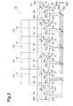
- Fig. 2 is a view showing with wiring the solid-state imaging device 10 shown in Fig. 1 .
- the solid-state imaging device 10 is a three-phase drive solid-state imaging device, and has terminals P1 to P3, PM1 to PM3, and PDC.
- the terminals P1 to P3 are terminals for inputting 3-phase clock signals to the output registers 18 and the corner registers 24 of all units 14a to 14d.
- the wirings extending from the terminals P1 to P3 are common to the output registers 18 and the corner registers 24 of all units 14a to 14d, and connected to the output registers 18 and the corner registers 24 of all units 14a to 14d.
- the output registers 18 and the corner registers 24 transfer charges, respectively.
- the wirings extending from these terminals P1 to P3 are also common to the dummy output registers 18d and the dummy corner registers 24d, and also connected to the dummy output registers 18d and the dummy corner registers 24d.
- the terminals PM1 to PM3 are terminals for inputting 3-phase clock signals to the multiplication registers 20 of all units 14a to 14d.
- the terminal PDC is a terminal to which a DC voltage is input for forming a barrier on the multiplication registers 20.
- the wirings extending from the terminals PM1 to PM3 and PDC are common to the multiplication registers 20 of all units 14a to 14d, and connected to the multiplication registers 20 of all units 14a to 14d. Further, the wirings extending from these terminals PM1 to PM3 and PDC are also common to the dummy multiplication registers 20d, and also connected to the multiplication registers 20d.
- Each of the amplifiers 22 and 22d has a reset gate terminal RG, a reset drain terminal RD, an output drain terminal OD, and an output source terminal OS. Moreover, between an FD region of the amplifiers 22, 22d and the last stage of the multiplication register 20, an output gate terminal OG is provided.
- the terminal RG is a terminal for supplying a reset pulse to the gates of a reset transistor in the amplifiers 22, 22d.
- a reset pulse being supplied to the terminal RG, a charge accumulated in the FD region is discharged from the terminal RD connected to the drain of the reset transistor.
- a predetermined supply voltage is supplied to the terminals RD and OD.
- an ON signal is supplied when transferring a charge from the multiplication register. Accordingly, the charge from the multiplication register is transferred to the FD region. From the terminal OS, an amplified signal is output.
- the same terminals of the amplifiers 22 and 22d are supplied with the same signals, but the wirings are not in common in order to prevent crosstalk between adjacent amplifiers.
- the multiplication register 20d and the amplifier 22d are provided in each of the first dummy region R1 and the second dummy region R2 located near the units 14a and 14d at both ends of the multiple units 14a to 14d.
- signals are supplied also to the multiplication register 20d and the amplifier 22d like the multiplication register 20 and the amplifier 22 of the units 14a to 14d. Accordingly, the multiplication register 20d and the amplifier 22d generate heat like the multiplication register 20 and the amplifier 22. Therefore, the difference between the temperature of the units 14a and 14d at both ends and the temperature of other units 14b and 14c is reduced. Hence, in the solid-state imaging device 10, the difference in gain among the units 14a to 14d is reduced.
- the present invention is not limited to the present embodiment described above, and can be variously modified.
- the solid-state imaging device of the present invention may not have the dummy output registers and dummy corner registers. This is because heat generation by the output register and corner register is small relative to that of the multiplication register and amplifier.
- the solid-state imaging device of the present invention is not limited to a three-phase drive solid-state imaging device, and can adopt various drive systems such as, for example, four-phase drive.
- 10 Solid-state image imaging device, 12 ... Imaging region, 14a to 14d ... Unit, 16 ... Charge accumulating region, 18 ... Output register, 18d ... Output register (dummy), 20 ... Multiplication register, 20d ... Multiplication register (dummy), 22 ... Amplifier, 22d ... Amplifier (dummy), 24 ... Corner register, 24d ... Corner register (dummy), OD ... Output drain terminal, OG ... Output gate terminal, OS ... Output source terminal, RD ... Reset drain terminal, RG ... Reset gate terminal, P1 to P3 ... Terminal, PDC ... Terminal, PM1 to PM3 ... Terminal, R ... Region, R1 ... First dummy region, R2 ... Second dummy region.
Landscapes
- Engineering & Computer Science (AREA)
- Multimedia (AREA)
- Signal Processing (AREA)
- Solid State Image Pick-Up Elements (AREA)
- Transforming Light Signals Into Electric Signals (AREA)
Abstract
Description
- The present invention relates to a multi-port type and charge multiplying type of solid-state imaging device.
- Among solid-state imaging device, there are multi-port and charge multiplying solid-state imaging devices described in the following Patent Literature 1 and Patent Literature 2. Such solid-state imaging devices include an imaging region and a plurality of units. The imaging region contains a plurality of pixel columns. Each of the units has an output register that transfers a charge from one or more corresponding pixel columns out of the pixel columns, a multiplication register that receives a charge transferred by the output register to generate a multiplied charge, and an amplifier that generates a signal based on a multiplied charge from the multiplication register.
-
- Patent Literature 1: Japanese Patent Laid-Open No.
2007-124675 - Patent Literature 2: Japanese Patent No.
3862850 - The gain of a charge multiplying solid-state imaging device fluctuates depending on the temperature. Moreover, it is desired from a multi-port and charge multiplying solid-state imaging devices to reduce a difference in gain in all units. The solid-state imaging device disclosed in Patent Literature 2 can control the multiplication register in multiplication factor, and is thus capable of controlling the gain of each port so as to reduce a difference in gain in all ports. However, a circuit configuration for controlling the gain is complicated.
- It is an object of the present invention to provide a multi-port and charge multiplying solid-state imaging device that outputs from a plurality of units signals based on charges from an imaging region, and that is capable of reducing a difference in gain among the units with a simple configuration.
- A solid-state imaging device of the present invention is a multi-port solid-state imaging device, and includes an imaging region and a plurality of units. The imaging region contains a plurality of pixel columns. The units are for generating a signal based on a charge from the imaging region, and arrayed in a direction in which the pixel columns are arrayed. Each of the units has an output register, a multiplication register, and an amplifier. The output register transfers a charge from one or more corresponding pixel columns out of the pixel columns. The multiplication register receives the charge from the output register to generate a multiplied charge. The amplifier generates a signal based on the multiplied charge from the multiplication register. The present solid-state imaging device contains a region where the units are provided, and a first dummy region and a second dummy region located on both sides in the above-mentioned direction of said region. In each of the first dummy region and the second dummy region, a multiplication register and an amplifier are provided.
- In a conventional multi-port and charge multiplying solid-state imaging device, the other units exist on both sides of units other than the units located at both ends of a plurality of units, but with regard to the units at both ends, one unit solely exists at one side thereof. Generally, the gain in each unit greatly fluctuates depending on the temperature of that unit. Moreover, heat generating elements such as an amplifier and a multiplication register are included in each unit. Therefore, in the conventional multi-port and charge multiplying solid-state imaging device, there is a difference produced between the temperature of the units at both ends and the temperature of other units. Hence, in the conventional multi-port and charge multiplying solid-state imaging device, it has been difficult to unify the gain among the units.
- On the other hand, according to the solid-state imaging device of the present invention, the multiplication register and the amplifier are provided near two units located at both ends of the multiple units. Therefore, the difference between the temperature of the two units located at both ends and the temperature of other units is reduced. Consequently, the difference in gain among the units is reduced.
- As has been described above, according to the present invention, a multi-port and charge multiplying solid-state imaging device that outputs from a plurality of units signals based on charges from an imaging region, and that is capable of reducing a difference in gain among the units with a simple configuration is provided.
-
-
Fig. 1 is a view showing a solid-state imaging device according to an embodiment. -
Fig. 2 is a view showing with wiring the solid-state imaging device shown inFig. 1 . - Hereinafter, a preferred embodiment of the present invention will be described in detail with reference to the drawings. Also, the same or corresponding parts will be denoted with the same reference numerals in the drawings.
-
Fig. 1 is a view showing a solid-state imaging device according to an embodiment. The solid-state imaging device 10 shown inFig. 1 includes animaging region 12, and a plurality ofunits 14a to 14d. In the following description, theunits 14a to 14d may be collectively referred to as units 14. - The
imaging region 12 is a region that generates charges in response to incident light. Specifically, theimaging region 12 includes a plurality of pixel arrayed two-dimensionally, and each pixel includes a photodiode. - The solid-
state imaging device 10 of the present embodiment includescharge accumulating regions 16 as well as theimaging region 12. Thecharge accumulating region 16 is a section that temporarily accumulates charges generated by theimaging region 12 before transferring the charges to output registers described later. The solid-state imaging device 10 having suchcharge accumulating regions 16 is called a frame transfer CCD image sensor. However, the solid-state imaging device of the present invention may be an interline CCD image sensor or a full-frame transfer CCD image sensor. - The
imaging region 12 has a plurality ofareas 12a to 12d. Theareas 12a to 12d are arranged in the horizontal direction, and a plurality of pixel columns are included in each area. Charges generated by theareas 12a to 12d are output to corresponding units 14. In addition, theimaging region 12 of the solid-state imaging device 10 contains four areas, that is, the solid-state imaging device 10 is a 4-port solid-state imaging device, but the number of ports of the solid-state imaging device of the present invention is not limited to four. - Each of the
units 14a to 14d has anoutput register 18, amultiplication register 20, and anamplifier 22. In the present embodiment, each of theunits 14a to 14d further may include acorner register 24. - The
output register 18 is a transfer register that receives a charge generated by a corresponding area of theimaging region 12 and then transferred in the vertical direction to transfer the charge in the horizontal direction. Thecorner register 24 is a transfer register that transfers a charge like theoutput register 18. Thecorner register 24 is provided between theoutput register 18 and themultiplication register 20. Thecorner register 24 transfers a charge transferred by theoutput register 18 to themultiplication register 20. - The
multiplication register 20 is a register that multiplies a charge by an impact ionization effect, and transfers the multiplied charge. In the solid-state imaging device 10, themultiplication register 20 receives via the corner register 24 a charge transferred from theoutput register 18, and outputs a multiplied charge to theamplifier 22. - The
amplifier 22 receives a charge multiplied by themultiplication register 20 to perform charge-voltage conversion, and generates a signal according to the amount of charge. As theamplifier 22, a floating diffusion (FD) amplifier may be used. - The present solid-
state imaging device 10 contains a region R, a first dummy region R1, and a second dummy region R2. The region R is a region where themultiple units 14a to 14d are provided. The first dummy region R1 and the second dummy region R2 exist on both sides of the region R in the same direction (horizontal direction) as the charge transferring direction of theoutput register 18. - The solid-
state imaging device 10 includes adummy multiplication register 20d and adummy amplifier 22d in each of the first dummy region R1 and the second dummy region R2. Thedummy multiplication register 20d and thedummy amplifier 22d are elements the same as themultiplication register 20 and theamplifier 22, respectively. - Further, in the solid-
state imaging device 10, adummy output register 18d and adummy corner register 24d may be provided in each of the first dummy region R1 and the second dummy region R2. Thedummy output register 18d and thedummy corner register 24d are elements the same as theoutput register 18 and thecorner register 24, respectively. - Hereinafter, the electrical connection relationship of the solid-
state imaging device 10 will be described with reference toFig. 2. Fig. 2 is a view showing with wiring the solid-state imaging device 10 shown inFig. 1 . As shown inFig. 2 , the solid-state imaging device 10 is a three-phase drive solid-state imaging device, and has terminals P1 to P3, PM1 to PM3, and PDC. - The terminals P1 to P3 are terminals for inputting 3-phase clock signals to the output registers 18 and the corner registers 24 of all
units 14a to 14d. The wirings extending from the terminals P1 to P3 are common to the output registers 18 and the corner registers 24 of allunits 14a to 14d, and connected to the output registers 18 and the corner registers 24 of allunits 14a to 14d. As a result of being supplied with 3-phase clock signals from the terminals P1 to P3, the output registers 18 and the corner registers 24 transfer charges, respectively. Further, the wirings extending from these terminals P1 to P3 are also common to thedummy output registers 18d and thedummy corner registers 24d, and also connected to thedummy output registers 18d and thedummy corner registers 24d. - The terminals PM1 to PM3 are terminals for inputting 3-phase clock signals to the multiplication registers 20 of all
units 14a to 14d. Moreover, the terminal PDC is a terminal to which a DC voltage is input for forming a barrier on the multiplication registers 20. The wirings extending from the terminals PM1 to PM3 and PDC are common to the multiplication registers 20 of allunits 14a to 14d, and connected to the multiplication registers 20 of allunits 14a to 14d. Further, the wirings extending from these terminals PM1 to PM3 and PDC are also common to thedummy multiplication registers 20d, and also connected to themultiplication registers 20d. - Each of the
amplifiers amplifiers multiplication register 20, an output gate terminal OG is provided. - The terminal RG is a terminal for supplying a reset pulse to the gates of a reset transistor in the
amplifiers - In the present solid-
state imaging device 10, the same terminals of theamplifiers - In the solid-
state imaging device 10 described above, themultiplication register 20d and theamplifier 22d are provided in each of the first dummy region R1 and the second dummy region R2 located near theunits multiple units 14a to 14d. In addition, signals are supplied also to themultiplication register 20d and theamplifier 22d like themultiplication register 20 and theamplifier 22 of theunits 14a to 14d. Accordingly, themultiplication register 20d and theamplifier 22d generate heat like themultiplication register 20 and theamplifier 22. Therefore, the difference between the temperature of theunits other units state imaging device 10, the difference in gain among theunits 14a to 14d is reduced. - It should be noted that the present invention is not limited to the present embodiment described above, and can be variously modified. For example, the solid-state imaging device of the present invention may not have the dummy output registers and dummy corner registers. This is because heat generation by the output register and corner register is small relative to that of the multiplication register and amplifier. Moreover, the solid-state imaging device of the present invention is not limited to a three-phase drive solid-state imaging device, and can adopt various drive systems such as, for example, four-phase drive.
- 10 ... Solid-state image imaging device, 12 ... Imaging region, 14a to 14d ... Unit, 16 ... Charge accumulating region, 18 ... Output register, 18d ... Output register (dummy), 20 ... Multiplication register, 20d ... Multiplication register (dummy), 22 ... Amplifier, 22d ... Amplifier (dummy), 24 ... Corner register, 24d ... Corner register (dummy), OD ... Output drain terminal, OG ... Output gate terminal, OS ... Output source terminal, RD ... Reset drain terminal, RG ... Reset gate terminal, P1 to P3 ... Terminal, PDC ... Terminal, PM1 to PM3 ... Terminal, R ... Region, R1 ... First dummy region, R2 ... Second dummy region.
Claims (1)
- A multi-port solid-state imaging device comprising:an imaging region containing a plurality of pixel columns; anda plurality of units that generate signals based on a charges from the imaging region, said units being arrayed in a direction in which the pixel columns are arrayed,each of the units having:an output register that transfers a charge from one or more corresponding pixel columns out of the plurality of pixel columns;a multiplication register that receives the charge from the output register to generate a multiplied charge; andan amplifier that generates a signal based on the multiplied charge from the multiplication register,wherein the solid-state imaging devicefurther comprises a region in which the units are provided, and a first dummy region and a second dummy region located on both sides in the direction of said region, andfurther comprises, in each of the first dummy region and the second dummy region, a multiplication register and an amplifier.
Applications Claiming Priority (2)
| Application Number | Priority Date | Filing Date | Title |
|---|---|---|---|
| JP2009020457A JP5237843B2 (en) | 2009-01-30 | 2009-01-30 | Solid-state imaging device |
| PCT/JP2010/050777 WO2010087278A1 (en) | 2009-01-30 | 2010-01-22 | Solid-state imaging device |
Publications (3)
| Publication Number | Publication Date |
|---|---|
| EP2247099A1 true EP2247099A1 (en) | 2010-11-03 |
| EP2247099A4 EP2247099A4 (en) | 2011-03-23 |
| EP2247099B1 EP2247099B1 (en) | 2012-03-21 |
Family
ID=42395540
Family Applications (1)
| Application Number | Title | Priority Date | Filing Date |
|---|---|---|---|
| EP10735747A Not-in-force EP2247099B1 (en) | 2009-01-30 | 2010-01-22 | Solid-state imaging device |
Country Status (8)
| Country | Link |
|---|---|
| US (1) | US8367999B2 (en) |
| EP (1) | EP2247099B1 (en) |
| JP (1) | JP5237843B2 (en) |
| KR (1) | KR101178670B1 (en) |
| CN (1) | CN101960837B (en) |
| AT (1) | ATE550874T1 (en) |
| TW (1) | TWI481257B (en) |
| WO (1) | WO2010087278A1 (en) |
Families Citing this family (6)
| Publication number | Priority date | Publication date | Assignee | Title |
|---|---|---|---|---|
| JP5330001B2 (en) * | 2009-01-30 | 2013-10-30 | 浜松ホトニクス株式会社 | Solid-state imaging device |
| US8773563B2 (en) | 2011-05-25 | 2014-07-08 | Truesense Imaging, Inc. | Multi-purpose architecture for CCD image sensors |
| US8411189B2 (en) * | 2011-05-25 | 2013-04-02 | Truesense Imaging, Inc. | Multi-purpose architecture for CCD image sensors |
| US8800130B2 (en) | 2011-05-25 | 2014-08-12 | Truesense Imaging, Inc. | Methods for producing image sensors having multi-purpose architecture |
| CN104767945B (en) * | 2015-04-14 | 2018-02-06 | 中国电子科技集团公司第四十四研究所 | The drive circuit of EMCCD transfer efficiencies can be improved |
| CN106601767B (en) * | 2016-12-02 | 2019-06-04 | 中国电子科技集团公司第四十四研究所 | Orthographic frame transfer CCD capable of reducing electrode signal delay |
Family Cites Families (25)
| Publication number | Priority date | Publication date | Assignee | Title |
|---|---|---|---|---|
| GB8901200D0 (en) | 1989-01-19 | 1989-03-15 | Eev Ltd | Camera using imaging array |
| KR100298039B1 (en) * | 1991-07-11 | 2001-10-24 | 윌리엄 비. 켐플러 | Charge multiplication device and manufacturing method |
| JP2785782B2 (en) * | 1995-12-27 | 1998-08-13 | 日本電気株式会社 | Solid-state imaging device |
| GB2323471B (en) | 1997-03-22 | 2002-04-17 | Eev Ltd | CCd imagers |
| JP3987232B2 (en) * | 1999-04-14 | 2007-10-03 | 日本放送協会 | Method for driving CCD type imaging device and CCD type imaging device |
| US6278142B1 (en) * | 1999-08-30 | 2001-08-21 | Isetex, Inc | Semiconductor image intensifier |
| JP2001119010A (en) * | 1999-10-18 | 2001-04-27 | Nikon Corp | Multi-output solid-state imaging device |
| EP1152469B1 (en) | 2000-04-28 | 2015-12-02 | Texas Instruments Japan Limited | High dynamic range charge readout system |
| US7420605B2 (en) * | 2001-01-18 | 2008-09-02 | E2V Technologies (Uk) Limited | Solid state imager arrangements |
| GB2371403B (en) * | 2001-01-18 | 2005-07-27 | Marconi Applied Techn Ltd | Solid state imager arrangements |
| US7190400B2 (en) * | 2001-06-04 | 2007-03-13 | Texas Instruments Incorporated | Charge multiplier with logarithmic dynamic range compression implemented in charge domain |
| JP3689866B2 (en) * | 2002-05-30 | 2005-08-31 | 日本テキサス・インスツルメンツ株式会社 | CMD and CCD device with CMD |
| US6791858B2 (en) * | 2002-08-26 | 2004-09-14 | Micron Technology, Inc. | Power reduction in CMOS imagers by trimming of master current reference |
| US20050029553A1 (en) * | 2003-08-04 | 2005-02-10 | Jaroslav Hynecek | Clocked barrier virtual phase charge coupled device image sensor |
| GB2413007A (en) * | 2004-04-07 | 2005-10-12 | E2V Tech Uk Ltd | Multiplication register for amplifying signal charge |
| US7692707B2 (en) | 2004-07-20 | 2010-04-06 | Shimadzu Corporation | Solid-state image pickup apparatus, image pickup apparatus, and image sensor |
| CN100539650C (en) * | 2004-07-20 | 2009-09-09 | 株式会社岛津制作所 | Solid-state imaging device, imaging device, and imaging element |
| JP4751617B2 (en) * | 2005-01-21 | 2011-08-17 | 株式会社日立ハイテクノロジーズ | Defect inspection method and apparatus |
| GB0503827D0 (en) * | 2005-02-24 | 2005-04-06 | E2V Tech Uk Ltd | Enhanced spectral range imaging sensor |
| JP4687155B2 (en) * | 2005-03-09 | 2011-05-25 | ソニー株式会社 | Solid-state imaging device and driving method thereof |
| GB2424758A (en) * | 2005-03-31 | 2006-10-04 | E2V Tech | CCD device |
| GB2431538B (en) * | 2005-10-24 | 2010-12-22 | E2V Tech | CCD device |
| US7755685B2 (en) * | 2007-09-28 | 2010-07-13 | Sarnoff Corporation | Electron multiplication CMOS imager |
| JP5346605B2 (en) * | 2009-01-30 | 2013-11-20 | 浜松ホトニクス株式会社 | Solid-state imaging device |
| GB2468668B (en) * | 2009-03-17 | 2014-07-16 | E2V Tech Uk Ltd | CCD imaging array with extended dynamic range |
-
2009
- 2009-01-30 JP JP2009020457A patent/JP5237843B2/en active Active
-
2010
- 2010-01-22 EP EP10735747A patent/EP2247099B1/en not_active Not-in-force
- 2010-01-22 WO PCT/JP2010/050777 patent/WO2010087278A1/en not_active Ceased
- 2010-01-22 US US12/920,142 patent/US8367999B2/en not_active Expired - Fee Related
- 2010-01-22 KR KR1020107015311A patent/KR101178670B1/en not_active Expired - Fee Related
- 2010-01-22 CN CN2010800011468A patent/CN101960837B/en not_active Expired - Fee Related
- 2010-01-22 AT AT10735747T patent/ATE550874T1/en active
- 2010-01-27 TW TW099102275A patent/TWI481257B/en not_active IP Right Cessation
Also Published As
| Publication number | Publication date |
|---|---|
| CN101960837B (en) | 2012-11-28 |
| US8367999B2 (en) | 2013-02-05 |
| JP5237843B2 (en) | 2013-07-17 |
| KR101178670B1 (en) | 2012-08-30 |
| TW201127031A (en) | 2011-08-01 |
| CN101960837A (en) | 2011-01-26 |
| TWI481257B (en) | 2015-04-11 |
| ATE550874T1 (en) | 2012-04-15 |
| EP2247099A4 (en) | 2011-03-23 |
| KR20100109550A (en) | 2010-10-08 |
| US20110031377A1 (en) | 2011-02-10 |
| EP2247099B1 (en) | 2012-03-21 |
| JP2010178194A (en) | 2010-08-12 |
| WO2010087278A1 (en) | 2010-08-05 |
Similar Documents
| Publication | Publication Date | Title |
|---|---|---|
| CN101369595B (en) | Solid-state image device | |
| US7990440B2 (en) | Image sensing apparatus and imaging system | |
| JP4818018B2 (en) | Photoelectric conversion device and imaging system using the same | |
| US8878971B2 (en) | Image sensing apparatus, image sensing apparatus control method, and imaging system | |
| US6552323B2 (en) | Image sensor with a shared output signal line | |
| JP4054839B1 (en) | Photoelectric conversion device and imaging system using the same | |
| US10658404B2 (en) | Solid state imaging device and imaging apparatus with pixel column having multiple output lines | |
| CN102244741B (en) | Solid-state image sensor and camera | |
| US7714920B2 (en) | Solid-state imaging device driving method | |
| US8367999B2 (en) | Solid state imaging device comprising dummy regions each containing a multiplication register and an amplifier | |
| US8552352B2 (en) | Solid-state imaging device including corner register | |
| US20130043373A1 (en) | Solid-state imaging device | |
| KR101594201B1 (en) | Solid-state imaging device | |
| JP4330579B2 (en) | Solid-state imaging device | |
| JP2009124495A (en) | Solid-state image sensor |
Legal Events
| Date | Code | Title | Description |
|---|---|---|---|
| PUAI | Public reference made under article 153(3) epc to a published international application that has entered the european phase |
Free format text: ORIGINAL CODE: 0009012 |
|
| 17P | Request for examination filed |
Effective date: 20100831 |
|
| AK | Designated contracting states |
Kind code of ref document: A1 Designated state(s): AT BE BG CH CY CZ DE DK EE ES FI FR GB GR HR HU IE IS IT LI LT LU LV MC MK MT NL NO PL PT RO SE SI SK SM TR |
|
| AX | Request for extension of the european patent |
Extension state: AL BA RS |
|
| A4 | Supplementary search report drawn up and despatched |
Effective date: 20110217 |
|
| GRAP | Despatch of communication of intention to grant a patent |
Free format text: ORIGINAL CODE: EPIDOSNIGR1 |
|
| DAX | Request for extension of the european patent (deleted) | ||
| GRAS | Grant fee paid |
Free format text: ORIGINAL CODE: EPIDOSNIGR3 |
|
| GRAA | (expected) grant |
Free format text: ORIGINAL CODE: 0009210 |
|
| AK | Designated contracting states |
Kind code of ref document: B1 Designated state(s): AT BE BG CH CY CZ DE DK EE ES FI FR GB GR HR HU IE IS IT LI LT LU LV MC MK MT NL NO PL PT RO SE SI SK SM TR |
|
| REG | Reference to a national code |
Ref country code: GB Ref legal event code: FG4D |
|
| REG | Reference to a national code |
Ref country code: CH Ref legal event code: EP |
|
| REG | Reference to a national code |
Ref country code: IE Ref legal event code: FG4D |
|
| REG | Reference to a national code |
Ref country code: AT Ref legal event code: REF Ref document number: 550874 Country of ref document: AT Kind code of ref document: T Effective date: 20120415 |
|
| REG | Reference to a national code |
Ref country code: DE Ref legal event code: R096 Ref document number: 602010001152 Country of ref document: DE Effective date: 20120516 |
|
| REG | Reference to a national code |
Ref country code: NL Ref legal event code: VDEP Effective date: 20120321 |
|
| PG25 | Lapsed in a contracting state [announced via postgrant information from national office to epo] |
Ref country code: LT Free format text: LAPSE BECAUSE OF FAILURE TO SUBMIT A TRANSLATION OF THE DESCRIPTION OR TO PAY THE FEE WITHIN THE PRESCRIBED TIME-LIMIT Effective date: 20120321 Ref country code: NO Free format text: LAPSE BECAUSE OF FAILURE TO SUBMIT A TRANSLATION OF THE DESCRIPTION OR TO PAY THE FEE WITHIN THE PRESCRIBED TIME-LIMIT Effective date: 20120621 Ref country code: HR Free format text: LAPSE BECAUSE OF FAILURE TO SUBMIT A TRANSLATION OF THE DESCRIPTION OR TO PAY THE FEE WITHIN THE PRESCRIBED TIME-LIMIT Effective date: 20120321 |
|
| LTIE | Lt: invalidation of european patent or patent extension |
Effective date: 20120321 |
|
| PG25 | Lapsed in a contracting state [announced via postgrant information from national office to epo] |
Ref country code: GR Free format text: LAPSE BECAUSE OF FAILURE TO SUBMIT A TRANSLATION OF THE DESCRIPTION OR TO PAY THE FEE WITHIN THE PRESCRIBED TIME-LIMIT Effective date: 20120622 Ref country code: FI Free format text: LAPSE BECAUSE OF FAILURE TO SUBMIT A TRANSLATION OF THE DESCRIPTION OR TO PAY THE FEE WITHIN THE PRESCRIBED TIME-LIMIT Effective date: 20120321 Ref country code: LV Free format text: LAPSE BECAUSE OF FAILURE TO SUBMIT A TRANSLATION OF THE DESCRIPTION OR TO PAY THE FEE WITHIN THE PRESCRIBED TIME-LIMIT Effective date: 20120321 |
|
| REG | Reference to a national code |
Ref country code: AT Ref legal event code: MK05 Ref document number: 550874 Country of ref document: AT Kind code of ref document: T Effective date: 20120321 |
|
| PG25 | Lapsed in a contracting state [announced via postgrant information from national office to epo] |
Ref country code: CY Free format text: LAPSE BECAUSE OF FAILURE TO SUBMIT A TRANSLATION OF THE DESCRIPTION OR TO PAY THE FEE WITHIN THE PRESCRIBED TIME-LIMIT Effective date: 20120321 |
|
| PG25 | Lapsed in a contracting state [announced via postgrant information from national office to epo] |
Ref country code: BE Free format text: LAPSE BECAUSE OF FAILURE TO SUBMIT A TRANSLATION OF THE DESCRIPTION OR TO PAY THE FEE WITHIN THE PRESCRIBED TIME-LIMIT Effective date: 20120321 Ref country code: EE Free format text: LAPSE BECAUSE OF FAILURE TO SUBMIT A TRANSLATION OF THE DESCRIPTION OR TO PAY THE FEE WITHIN THE PRESCRIBED TIME-LIMIT Effective date: 20120321 Ref country code: IS Free format text: LAPSE BECAUSE OF FAILURE TO SUBMIT A TRANSLATION OF THE DESCRIPTION OR TO PAY THE FEE WITHIN THE PRESCRIBED TIME-LIMIT Effective date: 20120721 Ref country code: CZ Free format text: LAPSE BECAUSE OF FAILURE TO SUBMIT A TRANSLATION OF THE DESCRIPTION OR TO PAY THE FEE WITHIN THE PRESCRIBED TIME-LIMIT Effective date: 20120321 Ref country code: SE Free format text: LAPSE BECAUSE OF FAILURE TO SUBMIT A TRANSLATION OF THE DESCRIPTION OR TO PAY THE FEE WITHIN THE PRESCRIBED TIME-LIMIT Effective date: 20120321 Ref country code: PL Free format text: LAPSE BECAUSE OF FAILURE TO SUBMIT A TRANSLATION OF THE DESCRIPTION OR TO PAY THE FEE WITHIN THE PRESCRIBED TIME-LIMIT Effective date: 20120321 Ref country code: SI Free format text: LAPSE BECAUSE OF FAILURE TO SUBMIT A TRANSLATION OF THE DESCRIPTION OR TO PAY THE FEE WITHIN THE PRESCRIBED TIME-LIMIT Effective date: 20120321 Ref country code: RO Free format text: LAPSE BECAUSE OF FAILURE TO SUBMIT A TRANSLATION OF THE DESCRIPTION OR TO PAY THE FEE WITHIN THE PRESCRIBED TIME-LIMIT Effective date: 20120321 |
|
| PG25 | Lapsed in a contracting state [announced via postgrant information from national office to epo] |
Ref country code: SK Free format text: LAPSE BECAUSE OF FAILURE TO SUBMIT A TRANSLATION OF THE DESCRIPTION OR TO PAY THE FEE WITHIN THE PRESCRIBED TIME-LIMIT Effective date: 20120321 Ref country code: PT Free format text: LAPSE BECAUSE OF FAILURE TO SUBMIT A TRANSLATION OF THE DESCRIPTION OR TO PAY THE FEE WITHIN THE PRESCRIBED TIME-LIMIT Effective date: 20120723 |
|
| PLBE | No opposition filed within time limit |
Free format text: ORIGINAL CODE: 0009261 |
|
| STAA | Information on the status of an ep patent application or granted ep patent |
Free format text: STATUS: NO OPPOSITION FILED WITHIN TIME LIMIT |
|
| PG25 | Lapsed in a contracting state [announced via postgrant information from national office to epo] |
Ref country code: DK Free format text: LAPSE BECAUSE OF FAILURE TO SUBMIT A TRANSLATION OF THE DESCRIPTION OR TO PAY THE FEE WITHIN THE PRESCRIBED TIME-LIMIT Effective date: 20120321 Ref country code: NL Free format text: LAPSE BECAUSE OF FAILURE TO SUBMIT A TRANSLATION OF THE DESCRIPTION OR TO PAY THE FEE WITHIN THE PRESCRIBED TIME-LIMIT Effective date: 20120321 Ref country code: AT Free format text: LAPSE BECAUSE OF FAILURE TO SUBMIT A TRANSLATION OF THE DESCRIPTION OR TO PAY THE FEE WITHIN THE PRESCRIBED TIME-LIMIT Effective date: 20120321 |
|
| 26N | No opposition filed |
Effective date: 20130102 |
|
| PG25 | Lapsed in a contracting state [announced via postgrant information from national office to epo] |
Ref country code: IT Free format text: LAPSE BECAUSE OF FAILURE TO SUBMIT A TRANSLATION OF THE DESCRIPTION OR TO PAY THE FEE WITHIN THE PRESCRIBED TIME-LIMIT Effective date: 20120321 |
|
| REG | Reference to a national code |
Ref country code: DE Ref legal event code: R097 Ref document number: 602010001152 Country of ref document: DE Effective date: 20130102 |
|
| PG25 | Lapsed in a contracting state [announced via postgrant information from national office to epo] |
Ref country code: ES Free format text: LAPSE BECAUSE OF FAILURE TO SUBMIT A TRANSLATION OF THE DESCRIPTION OR TO PAY THE FEE WITHIN THE PRESCRIBED TIME-LIMIT Effective date: 20120702 |
|
| PG25 | Lapsed in a contracting state [announced via postgrant information from national office to epo] |
Ref country code: BG Free format text: LAPSE BECAUSE OF FAILURE TO SUBMIT A TRANSLATION OF THE DESCRIPTION OR TO PAY THE FEE WITHIN THE PRESCRIBED TIME-LIMIT Effective date: 20120621 |
|
| PG25 | Lapsed in a contracting state [announced via postgrant information from national office to epo] |
Ref country code: MC Free format text: LAPSE BECAUSE OF NON-PAYMENT OF DUE FEES Effective date: 20130131 |
|
| REG | Reference to a national code |
Ref country code: IE Ref legal event code: MM4A |
|
| PG25 | Lapsed in a contracting state [announced via postgrant information from national office to epo] |
Ref country code: IE Free format text: LAPSE BECAUSE OF NON-PAYMENT OF DUE FEES Effective date: 20130122 |
|
| PG25 | Lapsed in a contracting state [announced via postgrant information from national office to epo] |
Ref country code: MT Free format text: LAPSE BECAUSE OF FAILURE TO SUBMIT A TRANSLATION OF THE DESCRIPTION OR TO PAY THE FEE WITHIN THE PRESCRIBED TIME-LIMIT Effective date: 20120321 |
|
| REG | Reference to a national code |
Ref country code: CH Ref legal event code: PL |
|
| PG25 | Lapsed in a contracting state [announced via postgrant information from national office to epo] |
Ref country code: CH Free format text: LAPSE BECAUSE OF NON-PAYMENT OF DUE FEES Effective date: 20140131 Ref country code: LI Free format text: LAPSE BECAUSE OF NON-PAYMENT OF DUE FEES Effective date: 20140131 |
|
| PG25 | Lapsed in a contracting state [announced via postgrant information from national office to epo] |
Ref country code: SM Free format text: LAPSE BECAUSE OF FAILURE TO SUBMIT A TRANSLATION OF THE DESCRIPTION OR TO PAY THE FEE WITHIN THE PRESCRIBED TIME-LIMIT Effective date: 20120321 |
|
| PG25 | Lapsed in a contracting state [announced via postgrant information from national office to epo] |
Ref country code: TR Free format text: LAPSE BECAUSE OF FAILURE TO SUBMIT A TRANSLATION OF THE DESCRIPTION OR TO PAY THE FEE WITHIN THE PRESCRIBED TIME-LIMIT Effective date: 20120321 |
|
| PG25 | Lapsed in a contracting state [announced via postgrant information from national office to epo] |
Ref country code: LU Free format text: LAPSE BECAUSE OF NON-PAYMENT OF DUE FEES Effective date: 20130122 Ref country code: HU Free format text: LAPSE BECAUSE OF FAILURE TO SUBMIT A TRANSLATION OF THE DESCRIPTION OR TO PAY THE FEE WITHIN THE PRESCRIBED TIME-LIMIT; INVALID AB INITIO Effective date: 20100122 Ref country code: MK Free format text: LAPSE BECAUSE OF FAILURE TO SUBMIT A TRANSLATION OF THE DESCRIPTION OR TO PAY THE FEE WITHIN THE PRESCRIBED TIME-LIMIT Effective date: 20120321 |
|
| REG | Reference to a national code |
Ref country code: FR Ref legal event code: PLFP Year of fee payment: 7 |
|
| REG | Reference to a national code |
Ref country code: FR Ref legal event code: PLFP Year of fee payment: 8 |
|
| REG | Reference to a national code |
Ref country code: FR Ref legal event code: PLFP Year of fee payment: 9 |
|
| PGFP | Annual fee paid to national office [announced via postgrant information from national office to epo] |
Ref country code: FR Payment date: 20191216 Year of fee payment: 11 |
|
| PGFP | Annual fee paid to national office [announced via postgrant information from national office to epo] |
Ref country code: DE Payment date: 20200107 Year of fee payment: 11 Ref country code: GB Payment date: 20200115 Year of fee payment: 11 |
|
| REG | Reference to a national code |
Ref country code: DE Ref legal event code: R119 Ref document number: 602010001152 Country of ref document: DE |
|
| GBPC | Gb: european patent ceased through non-payment of renewal fee |
Effective date: 20210122 |
|
| PG25 | Lapsed in a contracting state [announced via postgrant information from national office to epo] |
Ref country code: FR Free format text: LAPSE BECAUSE OF NON-PAYMENT OF DUE FEES Effective date: 20210131 |
|
| PG25 | Lapsed in a contracting state [announced via postgrant information from national office to epo] |
Ref country code: GB Free format text: LAPSE BECAUSE OF NON-PAYMENT OF DUE FEES Effective date: 20210122 Ref country code: DE Free format text: LAPSE BECAUSE OF NON-PAYMENT OF DUE FEES Effective date: 20210803 |