EP2247040A2 - buffered crossbar switch system - Google Patents
buffered crossbar switch system Download PDFInfo
- Publication number
- EP2247040A2 EP2247040A2 EP09175280A EP09175280A EP2247040A2 EP 2247040 A2 EP2247040 A2 EP 2247040A2 EP 09175280 A EP09175280 A EP 09175280A EP 09175280 A EP09175280 A EP 09175280A EP 2247040 A2 EP2247040 A2 EP 2247040A2
- Authority
- EP
- European Patent Office
- Prior art keywords
- data
- crossbar switch
- buffer
- input
- output
- Prior art date
- Legal status (The legal status is an assumption and is not a legal conclusion. Google has not performed a legal analysis and makes no representation as to the accuracy of the status listed.)
- Granted
Links
- 239000000872 buffer Substances 0.000 claims abstract description 76
- 239000004744 fabric Substances 0.000 claims abstract description 23
- 238000012546 transfer Methods 0.000 claims abstract description 12
- 230000015654 memory Effects 0.000 claims description 55
- 238000012545 processing Methods 0.000 claims description 32
- 238000013500 data storage Methods 0.000 claims description 12
- 230000004044 response Effects 0.000 claims description 2
- 238000004891 communication Methods 0.000 description 36
- 238000000034 method Methods 0.000 description 15
- 238000010586 diagram Methods 0.000 description 4
- 239000011159 matrix material Substances 0.000 description 3
- 230000003139 buffering effect Effects 0.000 description 2
- 230000006870 function Effects 0.000 description 2
- 230000003287 optical effect Effects 0.000 description 2
- 230000008569 process Effects 0.000 description 2
- 230000001174 ascending effect Effects 0.000 description 1
- 230000005540 biological transmission Effects 0.000 description 1
- 230000000903 blocking effect Effects 0.000 description 1
- 230000008878 coupling Effects 0.000 description 1
- 238000010168 coupling process Methods 0.000 description 1
- 238000005859 coupling reaction Methods 0.000 description 1
- 238000013461 design Methods 0.000 description 1
- 238000009429 electrical wiring Methods 0.000 description 1
- 230000005670 electromagnetic radiation Effects 0.000 description 1
- 239000000835 fiber Substances 0.000 description 1
- 239000000463 material Substances 0.000 description 1
- 239000013307 optical fiber Substances 0.000 description 1
- 238000012913 prioritisation Methods 0.000 description 1
- 239000007787 solid Substances 0.000 description 1
- 238000000638 solvent extraction Methods 0.000 description 1
- 238000009827 uniform distribution Methods 0.000 description 1
Images



Classifications
-
- H—ELECTRICITY
- H04—ELECTRIC COMMUNICATION TECHNIQUE
- H04L—TRANSMISSION OF DIGITAL INFORMATION, e.g. TELEGRAPHIC COMMUNICATION
- H04L49/00—Packet switching elements
- H04L49/25—Routing or path finding in a switch fabric
- H04L49/253—Routing or path finding in a switch fabric using establishment or release of connections between ports
- H04L49/254—Centralised controller, i.e. arbitration or scheduling
-
- H—ELECTRICITY
- H04—ELECTRIC COMMUNICATION TECHNIQUE
- H04L—TRANSMISSION OF DIGITAL INFORMATION, e.g. TELEGRAPHIC COMMUNICATION
- H04L49/00—Packet switching elements
- H04L49/10—Packet switching elements characterised by the switching fabric construction
- H04L49/101—Packet switching elements characterised by the switching fabric construction using crossbar or matrix
-
- H—ELECTRICITY
- H04—ELECTRIC COMMUNICATION TECHNIQUE
- H04L—TRANSMISSION OF DIGITAL INFORMATION, e.g. TELEGRAPHIC COMMUNICATION
- H04L49/00—Packet switching elements
- H04L49/25—Routing or path finding in a switch fabric
- H04L49/252—Store and forward routing
-
- H—ELECTRICITY
- H04—ELECTRIC COMMUNICATION TECHNIQUE
- H04L—TRANSMISSION OF DIGITAL INFORMATION, e.g. TELEGRAPHIC COMMUNICATION
- H04L49/00—Packet switching elements
- H04L49/30—Peripheral units, e.g. input or output ports
- H04L49/3027—Output queuing
-
- H—ELECTRICITY
- H04—ELECTRIC COMMUNICATION TECHNIQUE
- H04L—TRANSMISSION OF DIGITAL INFORMATION, e.g. TELEGRAPHIC COMMUNICATION
- H04L49/00—Packet switching elements
- H04L49/30—Peripheral units, e.g. input or output ports
- H04L49/3045—Virtual queuing
-
- H—ELECTRICITY
- H04—ELECTRIC COMMUNICATION TECHNIQUE
- H04L—TRANSMISSION OF DIGITAL INFORMATION, e.g. TELEGRAPHIC COMMUNICATION
- H04L49/00—Packet switching elements
- H04L49/50—Overload detection or protection within a single switching element
- H04L49/505—Corrective measures
- H04L49/508—Head of Line Blocking Avoidance
-
- H—ELECTRICITY
- H04—ELECTRIC COMMUNICATION TECHNIQUE
- H04Q—SELECTING
- H04Q3/00—Selecting arrangements
- H04Q3/0004—Selecting arrangements using crossbar selectors in the switching stages
-
- H—ELECTRICITY
- H04—ELECTRIC COMMUNICATION TECHNIQUE
- H04Q—SELECTING
- H04Q2213/00—Indexing scheme relating to selecting arrangements in general and for multiplex systems
- H04Q2213/1302—Relay switches
-
- H—ELECTRICITY
- H04—ELECTRIC COMMUNICATION TECHNIQUE
- H04Q—SELECTING
- H04Q2213/00—Indexing scheme relating to selecting arrangements in general and for multiplex systems
- H04Q2213/1304—Coordinate switches, crossbar, 4/2 with relays, coupling field
-
- H—ELECTRICITY
- H04—ELECTRIC COMMUNICATION TECHNIQUE
- H04Q—SELECTING
- H04Q2213/00—Indexing scheme relating to selecting arrangements in general and for multiplex systems
- H04Q2213/13076—Distributing frame, MDF, cross-connect switch
-
- H—ELECTRICITY
- H04—ELECTRIC COMMUNICATION TECHNIQUE
- H04Q—SELECTING
- H04Q2213/00—Indexing scheme relating to selecting arrangements in general and for multiplex systems
- H04Q2213/13103—Memory
-
- H—ELECTRICITY
- H04—ELECTRIC COMMUNICATION TECHNIQUE
- H04Q—SELECTING
- H04Q2213/00—Indexing scheme relating to selecting arrangements in general and for multiplex systems
- H04Q2213/13322—Integrated circuits
Definitions
- the present invention relates to a buffered crossbar switch for inter-connection between multiple modules in a communication system.
- a crossbar switch (also known as a "crosspoint switch” or a “matrix switch”) inter-connects a plurality of input ports and output ports to each other.
- a crossbar switch having P inputs and Q outputs has a switch fabric matrix with P x Q crosspoints where connections between input ports and output ports are made.
- packets arriving at one of the input ports might be routed to one or more specified output ports. For example, a packet might be routed to just a single specified output port (unicast), routed to all output ports (broadcast), or routed to multiple specified output ports (multicast).
- Bufferless crossbar switches are frequently used in multi-processor computer systems to link processors with other resources, such as memory or other subsystems, or with internet switches or other high-performance communication networks.
- bufferless crossbar switches generally require switch fabric speedup, meaning that the internal data rate of the switch must be higher than the data rate of the link.
- These crossbar switches typically require high-complexity centrally-controlled scheduling algorithms to achieve 100% throughput, such as the Parallel Iterative Matching (PIM) and iSLIP algorithms.
- PIM Parallel Iterative Matching
- iSLIP iSLIP
- buffers are included in the crossbar switch to temporarily store packets that cannot be routed to a specified output port instantly (i.e., blocked packets).
- buffers might be provided for each input port, for each output port, for each crosspoint connection of the crossbar switch, or some combination thereof.
- Centrally-controlled scheduling algorithms might be employed to allow the input and output data streams to efficiently access the switch fabric.
- the present invention provides for transfer of data between data modules.
- Each data module is at least one of a data processing module and a data storage module.
- At least two coupled crossbar switches are employed and input nodes and output nodes of each of the crossbar switches are coupled to corresponding data modules.
- the i th crossbar switch has an N i -input node by M i -output node switch fabric, wherein N i and M i are each positive integers greater than one.
- Each crossbar switch includes an input buffer at each input node, a crosspoint buffer at each crosspoint of the switch fabric, and an output buffer at each output node.
- the input buffer has an input arbiter that reads data packets from the input buffer in accordance with a first scheduling algorithm.
- the crosspoint buffer provides a queue having an output arbiter that reads data packets from the crosspoint buffer queue in accordance with a second scheduling algorithm.
- the output node receives segments of data packets provided from one or more corresponding crosspoint buffers.
- FIG. 1 shows a block diagram of a buffered crossbar switch system operating in accordance with exemplary embodiments of the present invention
- FIG. 2 shows a block diagram of a buffered crossbar switch in accordance with an embodiment of the present invention
- FIG. 3 shows additional detail of the buffered crossbar switch of FIG. 2 ;
- FIG. 4 shows another buffered crossbar switch system operating in accordance with exemplary embodiments of the present invention.
- FIG. 5 shows another buffered crossbar switch system operating in accordance with exemplary embodiments of the present invention.
- a buffered crossbar switch system for a high-throughput interconnection between multiple data modules in a communication system.
- embodiments of the present invention might be used to create concurrent virtual pipelines to interconnect multi-core processors with memory subsystems.
- Embodiments of the present invention might alternatively be used as, for example, client-server switches, internet routers, shared memory systems, or network switches.
- Embodiments of the present invention might achieve 100% throughput without speedup.
- FIG. 1 shows a block diagram of exemplary buffered crossbar switch system 100.
- buffered crossbar switch system 100 comprises processing unit 102, buffered crossbar switches 103 and 104, and memory unit 105.
- Buffered crossbar switches 103 and 104 are each in electrical communication with processing unit 102 and memory unit 105.
- buffered crossbar switches 103 and 104 might be configured to implement a high-throughput interconnection between multiple data modules within processing unit 102 and memory unit 105.
- buffered crossbar switches 103 and 104 might be on one or more chips in communication with processing unit 102 and memory unit 105 via optical fiber.
- processing unit 102 might be a multi-core processor.
- processing unit 102 might include N processors, where N is an integer greater than or equal to 1.
- processing unit 102 includes processor 120(1), processor 120(2), and so on, through the Nth processor 120( N ).
- processors might be, for example, implemented as general-purpose processors, such as PowerPC or ARM processors, or the processors might be, for example, implemented as accelerators for specialized functions such as digital signal processing or security protocol processing.
- Processing unit 102 also includes arbiter 122(1), arbiter 122(2), and so on, through the Nth arbiter 122( N ). As shown in FIG.
- processor 120(1) is in electrical communication with arbiter 122(1)
- processor 120(2) is in electrical communication with arbiter 122(2) and so on, through processor 120( N ) that is in electrical communication with arbiter 122(N).
- Each of arbiters 122(1) through 122( N ) has at least one input port and one output port for communication with processors 120(1) through 120( N ), respectively.
- memory unit 105 might employ memory controllers for coordination of reading and writing operations with memory.
- Memory might include, for example, at least one RAM buffer. Therefore, as shown in the exemplary embodiment, memory unit 105 might include M memory controllers for coordination of reading information from, and writing information to, one or more RAM buffers, where M is an integer greater than or equal to 1. Values for N and M might be equal, but are not necessarily equal.
- Memory is not limited to only a RAM buffer, and might be implemented with one or more other types of memory, such as flash memory.
- Memory unit 105 includes memory controllers 152(1) through memory controller 152( M ). Memory unit 105 also includes arbiters 150(1) through arbiter 150( M ). As shown in FIG.
- memory controller 152(1) is in electrical communication with arbiter 150(1)
- memory controller 152(2) is in electrical communication with arbiter 150(2)
- memory controller 152( M ) that is in electrical communication with arbiter 150( M ).
- Each of arbiters 150(1) through 150( M ) has at least one input port and one output port for communication with memory controllers 152(1) through 152( M ), respectively.
- Embodiments of the present invention might alternatively include a centralized arbiter for output arbitration. Other embodiments of the present invention might include a combination of localized and centralized arbiters.
- Buffered crossbar switches 103 and 104 include a switch fabric configured to allow any input to the switch to be transferred to any one or more outputs of the switch.
- buffered crossbar switch 103 has N input ports and M output ports
- buffered crossbar switch 104 has M input ports and N output ports, where N is the number of processors and M is the number of memory controllers.
- buffered crossbar switch 103 has N input ports, shown as 132(1) through 132 ( N ) , and M output ports, shown as 138(1) through 138( M ).
- Buffered crossbar switch 104 has M input ports, shown as 148(1) through 148( M ), and N output ports, shown as 142(1) through 142( N ). While two buffered crossbar switches are shown in FIG. 1 , the present invention is not so limited, and, thus, buffered crossbar switch system 100 might include up to B buffered crossbar switches, where B is an integer greater than or equal to 1.
- an exemplary embodiment of the present invention might include 5 buffered crossbar switches: one switch (not shown) to send addresses from processing unit 102 to memory unit 105, one switch (shown as buffered crossbar switch 103) to send data from processing unit 102 to memory unit 105, one switch (not shown) to send addresses from memory unit 105 to processing unit 102, one switch (shown as buffered crossbar switch 104) to send data from memory unit 105 to processing unit 102, and one switch (not shown) to send responses from the memory to the processors.
- buffered crossbar switch 103 is configured to switch data sent from processing unit 102 to memory unit 105
- buffered crossbar switch 104 is configured to switch data sent from memory unit 105 to processing unit 102.
- buffered crossbar switches 103 and 104 might be used to set which ones of N processors of processing unit 102 are in communication with which ones of the M memory controllers of memory unit 105.
- data provided from processor 120(1) of processing unit 102 might be provided to input port 132(1) of buffered crossbar switch 103.
- Arbiter 122(1) controls what data processor 120(1) provides to input port 132(1) of buffered crossbar switch 103.
- buffered crossbar switch 103 might be configured to provide this data to output port 138(2) of buffered crossbar switch 103.
- Arbiter 150(2) controls which crosspoint buffer is transferred to output port 138(2) of buffered crossbar switch 103.
- buffered crossbar switch 103 provides this data to memory controller 152(2) of memory unit 105.
- dashed arrows 135 and 136 indicate other exemplary data path settings of buffered crossbar switch 103.
- Buffered crossbar switch 103 might also be set to provide the data from one input port to multiple output ports.
- data from memory controller 152(1) of memory unit 105 might be provided to buffered crossbar switch 104 at input port 148(2).
- Arbiter 150(1) controls what data memory controller 152(1) provides to input port 148(2) of buffered crossbar switch 104. As indicated by dashed arrow 145, buffered crossbar switch 104 might be set to provide this data to one output, in this instance, output port 142(2), which provides the data to processor 120(2) of processing unit 102. Arbiter 122(2) controls which crosspoint buffer is transferred to output port 142(2) of buffered crossbar switch 104. Analogously, dashed arrows 144 and 146 indicate other exemplary data path settings of buffered crossbar switch 104.
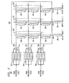
- FIG. 2 shows a block diagram of buffered crossbar switch system 200 in accordance with an embodiment of the present invention.
- buffered crossbar switch system 200 includes buffered crossbar switch 226 and virtual output queues (VOQs) 202, 204 and 206.
- Buffered crossbar switch 226 has 3 input ports, shown as input ports 220, 222 and 224, and 3 output ports, shown as output ports 246, 248 and 250.
- Input port 220 is in electrical communication with VOQ 202
- input port 222 is in electrical communication with VOQ 204
- input port 224 is in electrical communication with VOQ 206.
- Output port 246 is in electrical communication with output queue 1 252, output port 248 is in electrical communication with output queue 2 254 and output port 250 is in electrical communication with output queue M 256.
- Some embodiments of the present invention might not include output queues 252, 254 and 256.
- Buffered crossbar switch 226 includes a FIFO buffer at each crosspoint of the 3 x 3 switch matrix.
- an N x M switch will have N x M buffers.
- These FIFO buffers are shown in FIG. 2 as crosspoint queues 228, 230, 232, 234, 236, 238, 240 , 242 and 244.
- Crosspoint queues temporarily store data before forwarding the data to the respective output port. Crosspoint queues allow the switch fabric to receive data nearly simultaneously at multiple input ports without blocking.
- VOQs 202, 204 and 206 might each include one or more virtual first-in, first-out (FIFO) buffers.
- VOQ 202 might include three FIFOs, shown in FIG. 2 as FIFOs 202a, 202b and 202c; however, the present invention is not so limited and more or less FIFOs might be employed.
- Each VOQ buffer is in electrical communication with an arbiter that schedules access by the VOQs to the switch fabric of buffered crossbar switch 226.
- arbiter that schedules access by the VOQs to the switch fabric of buffered crossbar switch 226.
- VOQ 202 is in electrical communication with arbiter 214
- VOQ 204 is in electrical communication with arbiter 216
- VOQ 206 is in electrical communication with arbiter 218.
- FIG. 2 VOQs, embodiments of the present invention might employ other types of input buffering.
- Packets sent to VOQs 202, 204 and 206 are sorted in FIFOs according to the destination addresses of the packets.
- Packets generally are of a variable length, thus, embodiments of the present invention segment packets into "cells" before they are provided to the switch fabric.
- a cell is a fixed number of bits such that packets of varying sizes might be segmented into a number of cells of fixed size, plus padding, if necessary.
- Crosspoint queues temporarily store data cells before cells are transferred to corresponding output queue(s). Each crosspoint queue is in electrical communication with an arbiter that schedules access by the crosspoint queues to the output ports of buffered crossbar switch 226.
- crosspoint queues 228, 230 and 232 are in electrical communication with arbiter 225
- crosspoint queues 234, 236 and 238 are in electrical communication with arbiter 227
- crosspoint queues 240, 242 and 244 are in electrical communication with arbiter 229.
- arbiters 214, 216, and 218 correspond to arbiters 122(1) through 122( N )
- Some embodiments of the present invention include output queues 252, 254 and 256 to reassemble data cells into packets.
- Output queues 252, 254 and 256 are not needed in embodiments that send packets directly to the switch fabric (i.e. do not segment packets into cells) because no packet reassembly is required.
- each crosspoint queue e.g. queue depth
- the depth of each crosspoint queue might vary based on, for example, the round-trip time of data transfer through buffered crossbar switches 103 and 104 of FIG. 1 .
- a data path having a long round-trip time might require a larger crosspoint buffer to store data cells during the round-trip transfer of the packet.
- embodiments of the present invention provide crosspoint queues of varying depths to support different round-trip times.
- Round-trip time is the time required for a credit to return to the input arbiter and the time required to send data to a crosspoint buffer.
- All crosspoint buffers are empty.
- Each input arbiter of the buffered crossbar switch might track how many credits are available for each crosspoint buffer. For example, the number of credits, C , available for each input port i at crosspoint buffer i , j might be represented as C ( i , j ). The number of credits might initially be equal to the depth of crosspoint buffer i , j . For each data cell sent to crosspoint buffer i , j from input port i , the number of credits, C , is decremented.
- C ( i , j ) When C ( i , j ) is zero, input port i must stop sending data cells, or else crosspoint buffer i , j will overflow.
- C ( i , j ) When the output arbiter at output j pulls a cell from crosspoint buffer ( i , j ), C ( i , j ) is incremented ("returning a credit"). For example, in a system where it takes two cycles for an input to write to a crosspoint buffer and three cycles to return a credit, the round-trip time is 5 cycles. With a deeper crosspoint buffer, the input can keep sending cells into the crosspoint buffer without exhausting its credits. In exemplary embodiments of the present invention, the depth of the crosspoint buffer might increase as credit return latency, and thus round-trip time, increases.
- Input arbiters 214, 216 and 218 are distributed arbiters because each of N input FIFO buffers 202, 204 and 206 has one arbiter. Input arbiters are not in electrical communication with each other, thus facilitating scalability of buffered crossbar switch 226, since distributed arbiters might have a smaller physical size than a centralized arbiter. Similarly, output arbiters 225, 227 and 229 are also distributed arbiters because each of the M output queues 252, 254 and 256 has one arbiter.
- Arbiters 214, 216, 218, 225, 227 and 229 are, for exemplary embodiments, implemented as "round-robin" schedulers implementing a round-robin algorithm: buffers are processed in ascending or descending order, and the process returns to the first buffer in the sequence after the last buffer in the sequence is served. For example, as each one of non-empty VOQs 202a, 202b and 202c is served by arbiter 214, data cells in the serviced buffer are provided to the switch fabric until the currently serviced VOQ becomes empty or the timeslot for the VOQ is over. Either such occurrence causes arbiter 214 to advance to the next VOQ in the sequence.
- Arbiter 214 skips empty VOQs to serve the next non-empty VOQ.
- Arbiters 216, 218, 225, 227 and 229 operate similarly as arbiter 214.
- a round-robin scheduling algorithm is described, the present invention is not so limited, and other scheduling algorithms might be employed, for example longest queue first scheduling wherein the queue that has held data for the longest time is given scheduling priority. Further, embodiments of the present invention provide input and output arbiters that do not necessarily employ the same scheduling algorithm and a combination of scheduling algorithms might be employed.
- a packet consisting of Z cells might take N x Z clock cycles to reach the destination output queue.
- exemplary embodiments of the present invention provide for cell prioritization. For example, priority might be assigned on a processor basis, wherein certain processors within processing unit 102 might be assigned higher priority than other processors, such that the associated arbiter would deliver all Z cells of a packet consecutively in Z cycles. Alternatively, priority might be assigned on a packet basis, wherein, for example, certain types of packets might be assigned higher priority than other types of packets.
- Non-uniform output occurs with repeated access of a particular output port of buffered crossbar switch 226.
- Non-uniform output might limit the maximum throughput of buffered crossbar switch 226 since access to the output port is controlled by the output arbiter.
- each output port of buffered crossbar switch 226 corresponds to particular memory controller within memory unit 105.
- the destination memory address determines which output of the buffered crossbar switch 226 is accessed.
- sequential memory accesses might cause a non-uniform output condition to arise, which might limit the maximum throughput of buffered crossbar switch 226.
- Some embodiments of the present invention scramble memory addresses before passing data for such addresses through buffered crossbar switch 226. Scrambling of memory addresses translates sequential memory accesses into accesses having a more uniform distribution of output port accesses.
- FIG. 3 shows additional detail of the buffered crossbar switch system of FIG. 2 .
- exemplary embodiments of buffered crossbar switch 301 additionally include M multiplexers, shown as 302, 304 and 306, where M is the number of outputs of the crossbar switch.
- the switch fabric of buffered crossbar switch 301 might include M " N -to-1" multiplexers.
- arbiter 225 and crosspoint queues 228, 230 and 232 are in electrical communication with multiplexer 302.
- Arbiter 225 controls which of the crosspoint queues is asserted by multiplexer 302 to output port 246, thus accessing output queue 252.
- crosspoint queues 234, 236 and 238 are in electrical communication with multiplexer 304.
- Arbiter 227 controls which of the crosspoint queues is asserted by multiplexer 304 to output port 248, thus accessing output queue 254.
- Crosspoint queues 240, 242 and 244 are in electrical communication with multiplexer 306.
- Arbiter 229 controls which of the crosspoint queues is asserted by multiplexer 306 to output port 250, thus accessing output queue 256.
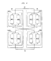
- each buffered crossbar switch might occupy its own circuit board, shown as switch cards 406(1) through 406( L ).
- Multiple switch cards might occupy a shelf, with multiple shelves, shown as shelves 404(1) through 404( K ), forming switch chassis 400.
- the processors and memories might be located on line chassis 402.
- Line chassis 402 might include multiple shelves, shown as shelves 409(1) through 409( K ), each shelf including multiple line cards, shown as line cards 410(1) through 410( L ).
- Each line card might contain devices, such as memory or processors, which communicate via the switch cards.
- a line chassis typically communicates with a switch chassis via electrical cables or optical links, shown as links 412, 414, 416 and 418.
- FIG. 5 shows another buffered crossbar switch system operating in accordance with exemplary embodiments of the present invention.
- one or more buffered crossbar switches shown as 500
- one or more buffered crossbar switches might be used to make a chain of processors 102 and storage modules 105 where a storage module might serve as a buffer for two processors to communicate with each other.
- Buffered crossbar switches 500 operate as described with regard to FIG. 1 .
- Buffered crossbar switches 500 might also be in electrical communication with bridge 502, thus, creating a branch along the chain.
- Bridge 500 might have one high-bandwidth port for communication with buffered crossbar switches 500, and lower bandwidth ports for communication with slower or legacy data modules, shown as processor 504 and storage modules 506 and 508.
- Bridge 502 might employ buffered crossbar switches as described above, or might employ a design that doesn't use buffered crossbar switches.
- circuits including possible implementation as a single integrated circuit, a multi-chip module, a single card, or a multi-card circuit pack
- present invention is not so limited.
- various functions of circuit elements may also be implemented as processing blocks in a software program.
- Such software may be employed in, for example, a digital signal processor, micro-controller, or general purpose computer.
- the present invention can be embodied in the form of methods and apparatuses for practicing those methods.
- the present invention can also be embodied in the form of program code embodied in tangible media, such as magnetic recording media, optical recording media, solid state memory, floppy diskettes, CD-ROMs, hard drives, or any other machine-readable storage medium, wherein, when the program code is loaded into and executed by a machine, such as a computer, the machine becomes an apparatus for practicing the invention.
- the present invention can also be embodied in the form of program code, for example, whether stored in a storage medium, loaded into and/or executed by a machine, or transmitted over some transmission medium or carrier, such as over electrical wiring or cabling, through fiber optics, or via electromagnetic radiation, wherein, when the program code is loaded into and executed by a machine, such as a computer, the machine becomes an apparatus for practicing the invention.
- program code When implemented on a general-purpose processor, the program code segments combine with the processor to provide a unique device that operates analogously to specific logic circuits.
- the present invention can also be embodied in the form of a bitstream or other sequence of signal values electrically or optically transmitted through a medium, stored magnetic-field variations in a magnetic recording medium, etc., generated using a method and/or an apparatus of the present invention.
- a method of transferring data between data modules is preferably provided, each of said data modules being at least one of a data processing module and a data storage module, the method comprising: passing the data through at least one crossbar switch, wherein input nodes and output nodes of each of the crossbar switches are coupled to corresponding ones of the data modules, the ith crossbar switch having an Ni-input node by Mi-output node switch fabric, wherein Ni and Mi are each positive integers greater than one and wherein each crossbar switch comprises: reading, from an input buffer at each input node having an input arbiter, data packets from each input buffer in accordance with a first scheduling algorithm; reading, from an output arbiter of a crosspoint buffer at each crosspoint of the switch fabric, the crosspoint buffer having a queue with an output arbiter, data packets from the crosspoint buffer queue in accordance with a second scheduling algorithm; and receiving, at an output node, segments of data packets from one or more corresponding crosspoint buffers.
- the method may further comprise varying, for each crosspoint buffer queue a depth of the queue in accordance with a round-trip time of data transfer through one of the at least one crossbar switch.
- the method may further comprise scrambling, when a data storage module employs sequential addressing of locations in memory, addresses of the locations in memory before passing the data through the at least one crossbar switch.
- the method may further comprise partitioning the packet of data provided to the input buffer into equal length cells.
- a machine-readable storage medium having encoded thereon program code, wherein, when the program code is executed by a machine, the machine implements a method for transferring data between data modules, each of said data modules being at least one of a data processing module and a data storage module, comprising the steps of: passing the data through at least one crossbar switch, wherein input nodes and output nodes of each of the crossbar switches are coupled to corresponding ones of the data modules, the ith crossbar switch having an Ni-input node by Mi-output node switch fabric, wherein Ni and Mi are each positive integers greater than one and wherein each crossbar switch comprises: reading, from an input buffer at each input node having an input arbiter, data packets from each input buffer in accordance with a first scheduling algorithm; reading, from an output arbiter of a crosspoint buffer at each crosspoint of the switch fabric, the crosspoint buffer having a queue with an output arbiter, data packets from the crosspoint buffer queue in accordance with a second scheduling algorithm; and receiving,
- the term "compatible" means that the element communicates with other elements in a manner wholly or partially specified by the standard, and would be recognized by other elements as sufficiently capable of communicating with the other elements in the manner specified by the standard.
- the compatible element does not need to operate internally in a manner specified by the standard.
- Couple refers to any manner known in the art or later developed in which energy is allowed to be transferred between two or more elements, and the interposition of one or more additional elements is contemplated, although not required.
- the terms “directly coupled,” “directly connected,” etc. imply the absence of such additional elements. Signals and corresponding nodes or ports may be referred to by the same name and are interchangeable for purposes here.
Landscapes
- Engineering & Computer Science (AREA)
- Computer Networks & Wireless Communication (AREA)
- Signal Processing (AREA)
- Physics & Mathematics (AREA)
- Mathematical Physics (AREA)
- Data Exchanges In Wide-Area Networks (AREA)
- Multi Processors (AREA)
Abstract
Description
- Field of the Invention
- The present invention relates to a buffered crossbar switch for inter-connection between multiple modules in a communication system.
- Description of the Related Art
- A crossbar switch (also known as a "crosspoint switch" or a "matrix switch") inter-connects a plurality of input ports and output ports to each other. A crossbar switch having P inputs and Q outputs has a switch fabric matrix with P x Q crosspoints where connections between input ports and output ports are made. Thus, packets arriving at one of the input ports might be routed to one or more specified output ports. For example, a packet might be routed to just a single specified output port (unicast), routed to all output ports (broadcast), or routed to multiple specified output ports (multicast).
- Bufferless crossbar switches are frequently used in multi-processor computer systems to link processors with other resources, such as memory or other subsystems, or with internet switches or other high-performance communication networks. However, bufferless crossbar switches generally require switch fabric speedup, meaning that the internal data rate of the switch must be higher than the data rate of the link. These crossbar switches typically require high-complexity centrally-controlled scheduling algorithms to achieve 100% throughput, such as the Parallel Iterative Matching (PIM) and iSLIP algorithms.
- In a buffered crossbar switch, buffers are included in the crossbar switch to temporarily store packets that cannot be routed to a specified output port instantly (i.e., blocked packets). For example, buffers might be provided for each input port, for each output port, for each crosspoint connection of the crossbar switch, or some combination thereof. Centrally-controlled scheduling algorithms might be employed to allow the input and output data streams to efficiently access the switch fabric.
- In an exemplary embodiment, the present invention provides for transfer of data between data modules. Each data module is at least one of a data processing module and a data storage module. At least two coupled crossbar switches are employed and input nodes and output nodes of each of the crossbar switches are coupled to corresponding data modules. The ith crossbar switch has an Ni -input node by Mi -output node switch fabric, wherein Ni and Mi are each positive integers greater than one. Each crossbar switch includes an input buffer at each input node, a crosspoint buffer at each crosspoint of the switch fabric, and an output buffer at each output node. The input buffer has an input arbiter that reads data packets from the input buffer in accordance with a first scheduling algorithm. The crosspoint buffer provides a queue having an output arbiter that reads data packets from the crosspoint buffer queue in accordance with a second scheduling algorithm. The output node receives segments of data packets provided from one or more corresponding crosspoint buffers.
- Other aspects, features, and advantages of the present invention will become more fully apparent from the following detailed description, the appended claims, and the accompanying drawings in which like reference numerals identify similar or identical elements.
-
FIG. 1 shows a block diagram of a buffered crossbar switch system operating in accordance with exemplary embodiments of the present invention; -
FIG. 2 shows a block diagram of a buffered crossbar switch in accordance with an embodiment of the present invention; -
FIG. 3 shows additional detail of the buffered crossbar switch ofFIG. 2 ; -
FIG. 4 shows another buffered crossbar switch system operating in accordance with exemplary embodiments of the present invention; and, -
FIG. 5 shows another buffered crossbar switch system operating in accordance with exemplary embodiments of the present invention. - In accordance with embodiments of the present invention, a buffered crossbar switch system is provided for a high-throughput interconnection between multiple data modules in a communication system. For example, through distributed buffering and scheduling algorithms in the crossbar switch, embodiments of the present invention might be used to create concurrent virtual pipelines to interconnect multi-core processors with memory subsystems. Embodiments of the present invention might alternatively be used as, for example, client-server switches, internet routers, shared memory systems, or network switches. Embodiments of the present invention might achieve 100% throughput without speedup.
-
FIG. 1 shows a block diagram of exemplary bufferedcrossbar switch system 100. As shown, bufferedcrossbar switch system 100 comprisesprocessing unit 102, bufferedcrossbar switches memory unit 105.Buffered crossbar switches processing unit 102 andmemory unit 105. Thus, as shown, bufferedcrossbar switches processing unit 102 andmemory unit 105. In some embodiments,buffered crossbar switches processing unit 102 andmemory unit 105 via optical fiber. - In some embodiments,
processing unit 102 might be a multi-core processor. For example,processing unit 102 might include N processors, where N is an integer greater than or equal to 1. As shown inFIG. 1 ,processing unit 102 includes processor 120(1), processor 120(2), and so on, through the Nth processor 120(N). Processors might be, for example, implemented as general-purpose processors, such as PowerPC or ARM processors, or the processors might be, for example, implemented as accelerators for specialized functions such as digital signal processing or security protocol processing.Processing unit 102 also includes arbiter 122(1), arbiter 122(2), and so on, through the Nth arbiter 122(N). As shown inFIG. 1 , processor 120(1) is in electrical communication with arbiter 122(1), processor 120(2) is in electrical communication with arbiter 122(2) and so on, through processor 120(N) that is in electrical communication with arbiter 122(N). Each of arbiters 122(1) through 122(N) has at least one input port and one output port for communication with processors 120(1) through 120(N), respectively. - In some embodiments,
memory unit 105 might employ memory controllers for coordination of reading and writing operations with memory. Memory might include, for example, at least one RAM buffer. Therefore, as shown in the exemplary embodiment,memory unit 105 might include M memory controllers for coordination of reading information from, and writing information to, one or more RAM buffers, where M is an integer greater than or equal to 1. Values for N and M might be equal, but are not necessarily equal. Memory is not limited to only a RAM buffer, and might be implemented with one or more other types of memory, such as flash memory.Memory unit 105 includes memory controllers 152(1) through memory controller 152(M).Memory unit 105 also includes arbiters 150(1) through arbiter 150(M). As shown inFIG. 1 , memory controller 152(1) is in electrical communication with arbiter 150(1), memory controller 152(2) is in electrical communication with arbiter 150(2), and so on, through memory controller 152(M) that is in electrical communication with arbiter 150(M). Each of arbiters 150(1) through 150(M) has at least one input port and one output port for communication with memory controllers 152(1) through 152(M), respectively. Embodiments of the present invention might alternatively include a centralized arbiter for output arbitration. Other embodiments of the present invention might include a combination of localized and centralized arbiters. - Buffered
crossbar switches buffered crossbar switch 103 has N input ports and M output ports, and bufferedcrossbar switch 104 has M input ports and N output ports, where N is the number of processors and M is the number of memory controllers. As shown inFIG. 1 ,buffered crossbar switch 103 has N input ports, shown as 132(1) through 132(N), and M output ports, shown as 138(1) through 138(M). Bufferedcrossbar switch 104 has M input ports, shown as 148(1) through 148(M), and N output ports, shown as 142(1) through 142(N). While two buffered crossbar switches are shown inFIG. 1 , the present invention is not so limited, and, thus, bufferedcrossbar switch system 100 might include up to B buffered crossbar switches, where B is an integer greater than or equal to 1. - For example, an exemplary embodiment of the present invention might include 5 buffered crossbar switches: one switch (not shown) to send addresses from
processing unit 102 tomemory unit 105, one switch (shown as buffered crossbar switch 103) to send data fromprocessing unit 102 tomemory unit 105, one switch (not shown) to send addresses frommemory unit 105 toprocessing unit 102, one switch (shown as buffered crossbar switch 104) to send data frommemory unit 105 toprocessing unit 102, and one switch (not shown) to send responses from the memory to the processors. - As shown in
FIG. 1 , bufferedcrossbar switch 103 is configured to switch data sent fromprocessing unit 102 tomemory unit 105, and bufferedcrossbar switch 104 is configured to switch data sent frommemory unit 105 toprocessing unit 102. Thus, buffered crossbar switches 103 and 104 might be used to set which ones of N processors ofprocessing unit 102 are in communication with which ones of the M memory controllers ofmemory unit 105. For example, data provided from processor 120(1) ofprocessing unit 102 might be provided to input port 132(1) of bufferedcrossbar switch 103. Arbiter 122(1) controls what data processor 120(1) provides to input port 132(1) of bufferedcrossbar switch 103. As indicated by dashedarrow 134, bufferedcrossbar switch 103 might be configured to provide this data to output port 138(2) of bufferedcrossbar switch 103. Arbiter 150(2) controls which crosspoint buffer is transferred to output port 138(2) of bufferedcrossbar switch 103. Thus, bufferedcrossbar switch 103 provides this data to memory controller 152(2) ofmemory unit 105. Analogously, dashedarrows 135 and 136 indicate other exemplary data path settings of bufferedcrossbar switch 103. Bufferedcrossbar switch 103 might also be set to provide the data from one input port to multiple output ports. Similarly, data from memory controller 152(1) ofmemory unit 105 might be provided to bufferedcrossbar switch 104 at input port 148(2). Arbiter 150(1) controls what data memory controller 152(1) provides to input port 148(2) of bufferedcrossbar switch 104. As indicated by dashedarrow 145, bufferedcrossbar switch 104 might be set to provide this data to one output, in this instance, output port 142(2), which provides the data to processor 120(2) ofprocessing unit 102. Arbiter 122(2) controls which crosspoint buffer is transferred to output port 142(2) of bufferedcrossbar switch 104. Analogously, dashedarrows crossbar switch 104. -
FIG. 2 shows a block diagram of buffered crossbar switch system 200 in accordance with an embodiment of the present invention. As shown, buffered crossbar switch system 200 includes bufferedcrossbar switch 226 and virtual output queues (VOQs) 202, 204 and 206. Bufferedcrossbar switch 226 has 3 input ports, shown asinput ports output ports FIG. 2 , N = M = 3.Input port 220 is in electrical communication withVOQ 202,input port 222 is in electrical communication withVOQ 204 andinput port 224 is in electrical communication withVOQ 206.Output port 246 is in electrical communication withoutput queue 1 252,output port 248 is in electrical communication withoutput queue 2 254 andoutput port 250 is in electrical communication withoutput queue M 256. Some embodiments of the present invention might not includeoutput queues crossbar switch 226 includes a FIFO buffer at each crosspoint of the 3 x 3 switch matrix. Thus, in exemplary embodiments, an N x M switch will have N x M buffers. These FIFO buffers are shown inFIG. 2 ascrosspoint queues -
VOQs VOQ 202 might include three FIFOs, shown inFIG. 2 as FIFOs 202a, 202b and 202c; however, the present invention is not so limited and more or less FIFOs might be employed. Each VOQ buffer is in electrical communication with an arbiter that schedules access by the VOQs to the switch fabric of bufferedcrossbar switch 226. As shown inFIG. 2 ,VOQ 202 is in electrical communication witharbiter 214,VOQ 204 is in electrical communication witharbiter 216 andVOQ 206 is in electrical communication witharbiter 218. Although shown inFIG. 2 as VOQs, embodiments of the present invention might employ other types of input buffering. - Packets sent to
VOQs crossbar switch 226. As shown,crosspoint queues arbiter 225,crosspoint queues arbiter 227 andcrosspoint queues arbiter 229. Referring back toFIG. 1 ,arbiters arbiters - Some embodiments of the present invention include
output queues Output queues - Some embodiments of the present invention provide that the size of each crosspoint queue (e.g. queue depth) might be variable. Thus, the depth of each crosspoint queue might vary based on, for example, the round-trip time of data transfer through buffered crossbar switches 103 and 104 of
FIG. 1 . For example, a data path having a long round-trip time might require a larger crosspoint buffer to store data cells during the round-trip transfer of the packet. Thus, embodiments of the present invention provide crosspoint queues of varying depths to support different round-trip times. - Round-trip time is the time required for a credit to return to the input arbiter and the time required to send data to a crosspoint buffer. Initially, all crosspoint buffers are empty. Each input arbiter of the buffered crossbar switch might track how many credits are available for each crosspoint buffer. For example, the number of credits, C, available for each input port i at crosspoint buffer i, j might be represented as C(i, j). The number of credits might initially be equal to the depth of crosspoint buffer i, j. For each data cell sent to crosspoint buffer i, j from input port i, the number of credits, C, is decremented. When C(i, j) is zero, input port i must stop sending data cells, or else crosspoint buffer i, j will overflow. When the output arbiter at output j pulls a cell from crosspoint buffer (i, j), C(i, j) is incremented ("returning a credit"). For example, in a system where it takes two cycles for an input to write to a crosspoint buffer and three cycles to return a credit, the round-trip time is 5 cycles. With a deeper crosspoint buffer, the input can keep sending cells into the crosspoint buffer without exhausting its credits. In exemplary embodiments of the present invention, the depth of the crosspoint buffer might increase as credit return latency, and thus round-trip time, increases.
-
Input arbiters crossbar switch 226, since distributed arbiters might have a smaller physical size than a centralized arbiter. Similarly,output arbiters M output queues -
Arbiters arbiter 214, data cells in the serviced buffer are provided to the switch fabric until the currently serviced VOQ becomes empty or the timeslot for the VOQ is over. Either such occurrence causesarbiter 214 to advance to the next VOQ in the sequence.Arbiter 214 skips empty VOQs to serve the next non-empty VOQ.Arbiters arbiter 214. Although a round-robin scheduling algorithm is described, the present invention is not so limited, and other scheduling algorithms might be employed, for example longest queue first scheduling wherein the queue that has held data for the longest time is given scheduling priority. Further, embodiments of the present invention provide input and output arbiters that do not necessarily employ the same scheduling algorithm and a combination of scheduling algorithms might be employed. - Generally, arbitration is performed as described above. Thus, if buffered
crossbar switch 226 has an equal number, N, of inputs and outputs, a packet consisting of Z cells, where Z is an integer, might take N x Z clock cycles to reach the destination output queue. Exemplary embodiments of the present invention provide for cell prioritization. For example, priority might be assigned on a processor basis, wherein certain processors withinprocessing unit 102 might be assigned higher priority than other processors, such that the associated arbiter would deliver all Z cells of a packet consecutively in Z cycles. Alternatively, priority might be assigned on a packet basis, wherein, for example, certain types of packets might be assigned higher priority than other types of packets. - Non-uniform output occurs with repeated access of a particular output port of buffered
crossbar switch 226. Non-uniform output might limit the maximum throughput of bufferedcrossbar switch 226 since access to the output port is controlled by the output arbiter. For example, as shown inFIG. 1 , each output port of bufferedcrossbar switch 226 corresponds to particular memory controller withinmemory unit 105. Typically, data transfer of a block of memory having sequential addresses is managed by one memory controller. The destination memory address determines which output of the bufferedcrossbar switch 226 is accessed. Thus, sequential memory accesses might cause a non-uniform output condition to arise, which might limit the maximum throughput of bufferedcrossbar switch 226. Some embodiments of the present invention scramble memory addresses before passing data for such addresses through bufferedcrossbar switch 226. Scrambling of memory addresses translates sequential memory accesses into accesses having a more uniform distribution of output port accesses. -
FIG. 3 shows additional detail of the buffered crossbar switch system ofFIG. 2 . As shown inFIG. 3 , exemplary embodiments of bufferedcrossbar switch 301 additionally include M multiplexers, shown as 302, 304 and 306, where M is the number of outputs of the crossbar switch. As shown inFIG. 3 , N = M = 3. For a switch having N inputs and M outputs, the switch fabric of bufferedcrossbar switch 301 might include M "N-to-1" multiplexers. As shown,arbiter 225 andcrosspoint queues multiplexer 302.Arbiter 225 controls which of the crosspoint queues is asserted bymultiplexer 302 tooutput port 246, thus accessingoutput queue 252. Similarly,crosspoint queues multiplexer 304.Arbiter 227 controls which of the crosspoint queues is asserted bymultiplexer 304 tooutput port 248, thus accessingoutput queue 254.Crosspoint queues multiplexer 306.Arbiter 229 controls which of the crosspoint queues is asserted bymultiplexer 306 tooutput port 250, thus accessingoutput queue 256. - While described above as being implemented as a monolithic chip, the present invention is not so limited. For example, as shown in
FIG. 4 , each buffered crossbar switch might occupy its own circuit board, shown as switch cards 406(1) through 406(L). Multiple switch cards might occupy a shelf, with multiple shelves, shown as shelves 404(1) through 404(K), formingswitch chassis 400. Similarly, the processors and memories might be located online chassis 402.Line chassis 402 might include multiple shelves, shown as shelves 409(1) through 409(K), each shelf including multiple line cards, shown as line cards 410(1) through 410(L). Each line card might contain devices, such as memory or processors, which communicate via the switch cards. A line chassis typically communicates with a switch chassis via electrical cables or optical links, shown aslinks -
FIG. 5 shows another buffered crossbar switch system operating in accordance with exemplary embodiments of the present invention. As shown inFIG. 5 , one or more buffered crossbar switches, shown as 500, might be used to make a chain ofprocessors 102 andstorage modules 105 where a storage module might serve as a buffer for two processors to communicate with each other. Buffered crossbar switches 500 operate as described with regard toFIG. 1 . Buffered crossbar switches 500 might also be in electrical communication withbridge 502, thus, creating a branch along the chain.Bridge 500 might have one high-bandwidth port for communication with buffered crossbar switches 500, and lower bandwidth ports for communication with slower or legacy data modules, shown asprocessor 504 andstorage modules Bridge 502 might employ buffered crossbar switches as described above, or might employ a design that doesn't use buffered crossbar switches. - It will be further understood that various changes in the details, materials, and arrangements of the parts which have been described and illustrated in order to explain the nature of this invention may be made by those skilled in the art without departing from the scope of the invention as expressed in the following claims.
- Reference herein to "one embodiment" or "an embodiment" means that a particular feature, structure, or characteristic described in connection with the embodiment can be included in at least one embodiment of the invention. The appearances of the phrase "in one embodiment" in various places in the specification are not necessarily all referring to the same embodiment, nor are separate or alternative embodiments necessarily mutually exclusive of other embodiments. The same applies to the term "implementation."
- While the exemplary embodiments of the present invention have been described with respect to processes of circuits, including possible implementation as a single integrated circuit, a multi-chip module, a single card, or a multi-card circuit pack, the present invention is not so limited. As would be apparent to one skilled in the art, various functions of circuit elements may also be implemented as processing blocks in a software program. Such software may be employed in, for example, a digital signal processor, micro-controller, or general purpose computer.
- The present invention can be embodied in the form of methods and apparatuses for practicing those methods. The present invention can also be embodied in the form of program code embodied in tangible media, such as magnetic recording media, optical recording media, solid state memory, floppy diskettes, CD-ROMs, hard drives, or any other machine-readable storage medium, wherein, when the program code is loaded into and executed by a machine, such as a computer, the machine becomes an apparatus for practicing the invention. The present invention can also be embodied in the form of program code, for example, whether stored in a storage medium, loaded into and/or executed by a machine, or transmitted over some transmission medium or carrier, such as over electrical wiring or cabling, through fiber optics, or via electromagnetic radiation, wherein, when the program code is loaded into and executed by a machine, such as a computer, the machine becomes an apparatus for practicing the invention. When implemented on a general-purpose processor, the program code segments combine with the processor to provide a unique device that operates analogously to specific logic circuits. The present invention can also be embodied in the form of a bitstream or other sequence of signal values electrically or optically transmitted through a medium, stored magnetic-field variations in a magnetic recording medium, etc., generated using a method and/or an apparatus of the present invention.
- A method of transferring data between data modules, is preferably provided, each of said data modules being at least one of a data processing module and a data storage module, the method comprising: passing the data through at least one crossbar switch, wherein input nodes and output nodes of each of the crossbar switches are coupled to corresponding ones of the data modules, the ith crossbar switch having an Ni-input node by Mi-output node switch fabric, wherein Ni and Mi are each positive integers greater than one and wherein each crossbar switch comprises: reading, from an input buffer at each input node having an input arbiter, data packets from each input buffer in accordance with a first scheduling algorithm; reading, from an output arbiter of a crosspoint buffer at each crosspoint of the switch fabric, the crosspoint buffer having a queue with an output arbiter, data packets from the crosspoint buffer queue in accordance with a second scheduling algorithm; and receiving, at an output node, segments of data packets from one or more corresponding crosspoint buffers.
- The method may further comprise varying, for each crosspoint buffer queue a depth of the queue in accordance with a round-trip time of data transfer through one of the at least one crossbar switch.
- The method may further comprise scrambling, when a data storage module employs sequential addressing of locations in memory, addresses of the locations in memory before passing the data through the at least one crossbar switch.
- The method may further comprise partitioning the packet of data provided to the input buffer into equal length cells.
- A machine-readable storage medium is preferably provided, having encoded thereon program code, wherein, when the program code is executed by a machine, the machine implements a method for transferring data between data modules, each of said data modules being at least one of a data processing module and a data storage module, comprising the steps of: passing the data through at least one crossbar switch, wherein input nodes and output nodes of each of the crossbar switches are coupled to corresponding ones of the data modules, the ith crossbar switch having an Ni-input node by Mi-output node switch fabric, wherein Ni and Mi are each positive integers greater than one and wherein each crossbar switch comprises: reading, from an input buffer at each input node having an input arbiter, data packets from each input buffer in accordance with a first scheduling algorithm; reading, from an output arbiter of a crosspoint buffer at each crosspoint of the switch fabric, the crosspoint buffer having a queue with an output arbiter, data packets from the crosspoint buffer queue in accordance with a second scheduling algorithm; and receiving, at an output node, segments of data packets from one or more corresponding crosspoint buffers.
- It should be understood that the steps of the exemplary methods set forth herein are not necessarily required to be performed in the order described, and the order of the steps of such methods should be understood to be merely exemplary. Likewise, additional steps may be included in such methods, and certain steps may be omitted or combined, in methods consistent with various embodiments of the present invention.
- As used herein in reference to an element and a standard, the term "compatible" means that the element communicates with other elements in a manner wholly or partially specified by the standard, and would be recognized by other elements as sufficiently capable of communicating with the other elements in the manner specified by the standard. The compatible element does not need to operate internally in a manner specified by the standard.
- Also for purposes of this description, the terms "couple," "coupling," "coupled," "electrical communication," "connect," "connecting," or "connected" refer to any manner known in the art or later developed in which energy is allowed to be transferred between two or more elements, and the interposition of one or more additional elements is contemplated, although not required. Conversely, the terms "directly coupled," "directly connected," etc., imply the absence of such additional elements. Signals and corresponding nodes or ports may be referred to by the same name and are interchangeable for purposes here.
Claims (15)
- Apparatus for transferring data between data modules, each of said data modules being at least one of a data processing module and a data storage module, the apparatus comprising:at least one crossbar switch, wherein input nodes and output nodes of each of the crossbar switches are coupled to corresponding ones of the data modules, the ith crossbar switch having an Ni-input node by Mi-output node switch fabric, wherein Ni and Mi are each positive integers greater than one and wherein each crossbar switch comprises:an input buffer at each input node having an input arbiter configured to read data packets from each input buffer in accordance with a first scheduling algorithm;a crosspoint buffer at each crosspoint of the switch fabric, the crosspoint buffer providing a queue having an output arbiter configured to read data packets from the crosspoint buffer queue in accordance with a second scheduling algorithm; andan output node configured to receive segments of data packets provided from one or more corresponding crosspoint buffers.
- The invention as recited in claim 1, further comprising an output buffer at each output node, the output buffer configured to store segments of data packets provided from one or more corresponding crosspoint buffers.
- The invention as recited in claim 1, wherein the input buffer at each input node further comprises one of: a first-in, first-out (FIFO) buffer, a virtual output queue (VOQ), or a push-in, first-out buffer (PIFO).
- The invention as recited in claim 1, wherein, for each crosspoint buffer queue a depth of the queue varies in accordance with a round-trip time of data transfer through one of the at least one crossbar switch.
- The invention as recited in claim 1, wherein at least one of the first scheduling algorithm and the second scheduling algorithm use a round-robin scheduling algorithm.
- The invention as recited in claim 5, wherein the round-robin scheduling algorithm of at least one of the first scheduling algorithm and the second scheduling algorithm employs priority delivery for one or more data processing modules.
- The invention as recited in claim 1, wherein, when a data storage module employs sequential addressing of locations in memory, addresses of the locations in memory are scrambled before passing the data through the at least one crossbar switch.
- The invention as recited in claim 1, wherein at least one Ni-input node by Mi-output node switch fabric comprises Mi inter-coupled Ni-to-1 multiplexers.
- The invention as recited in claim 1, wherein, the packet of data provided to the input buffer is partitioned into equal length cells.
- The invention as recited in claim 9, wherein the input buffer is a first-in, first-out (FIFO) buffer.
- The invention as recited in claim 1, wherein the apparatus comprises at least one pair of crossbar switches, a first crossbar switch has an N-input node by M-output node switch fabric, and a second crossbar switch has an M-input node by N-output node switch fabric, where N and M are each positive integers greater than or equal to one.
- The invention as recited in claim 11, wherein the first crossbar switch directs data from a first group of data modules to a second group of data modules, and the second crossbar switch directs data from the second group of data modules to the first group of data modules.
- The invention as recited in claim 12, wherein each of the first group of data modules is a data processing module and each of the second group of data modules is a data storage module.
- The invention as recited in claim 1, wherein, the apparatus is implemented in a monolithic integrated circuit chip.
- The invention as recited in claim 1, wherein the apparatus comprises at least five crossbar switches: a first crossbar switch for transfer of address data from a data processing module to a data storage module, a second crossbar switch for transfer of user data from the data processing module to the data storage module, a third crossbar switch for transfer of address data from the data storage module to the data processing module, a fourth crossbar switch for transfer of user data from the data storage module to the data processing module, and a fifth crossbar switch for transfer of responses from the data storage module to the data processing module.
Applications Claiming Priority (1)
| Application Number | Priority Date | Filing Date | Title |
|---|---|---|---|
| US12/430,438 US8352669B2 (en) | 2009-04-27 | 2009-04-27 | Buffered crossbar switch system |
Publications (3)
| Publication Number | Publication Date |
|---|---|
| EP2247040A2 true EP2247040A2 (en) | 2010-11-03 |
| EP2247040A3 EP2247040A3 (en) | 2011-12-07 |
| EP2247040B1 EP2247040B1 (en) | 2017-08-16 |
Family
ID=42536429
Family Applications (1)
| Application Number | Title | Priority Date | Filing Date |
|---|---|---|---|
| EP09175280.8A Not-in-force EP2247040B1 (en) | 2009-04-27 | 2009-11-06 | Buffered crossbar switch system |
Country Status (6)
| Country | Link |
|---|---|
| US (1) | US8352669B2 (en) |
| EP (1) | EP2247040B1 (en) |
| JP (1) | JP5537956B2 (en) |
| KR (1) | KR101639438B1 (en) |
| CN (1) | CN101873253B (en) |
| TW (1) | TWI390913B (en) |
Families Citing this family (38)
| Publication number | Priority date | Publication date | Assignee | Title |
|---|---|---|---|---|
| US7965705B2 (en) * | 2009-03-19 | 2011-06-21 | Oracle America, Inc. | Fast and fair arbitration on a data link |
| US9444757B2 (en) | 2009-04-27 | 2016-09-13 | Intel Corporation | Dynamic configuration of processing modules in a network communications processor architecture |
| CN101631081B (en) * | 2009-08-12 | 2011-06-08 | 华为技术有限公司 | Multistage switched network |
| US8687629B1 (en) * | 2009-11-18 | 2014-04-01 | Juniper Networks, Inc. | Fabric virtualization for packet and circuit switching |
| FR2955992B1 (en) * | 2010-01-29 | 2012-04-20 | Inst Nat Rech Inf Automat | MODULATING SWITCHING OR ROUTING DEVICE |
| US9432298B1 (en) | 2011-12-09 | 2016-08-30 | P4tents1, LLC | System, method, and computer program product for improving memory systems |
| US20130141442A1 (en) * | 2011-12-06 | 2013-06-06 | John W. Brothers | Method and apparatus for multi-chip processing |
| US8868672B2 (en) | 2012-05-14 | 2014-10-21 | Advanced Micro Devices, Inc. | Server node interconnect devices and methods |
| US9137173B2 (en) | 2012-06-19 | 2015-09-15 | Advanced Micro Devices, Inc. | Devices and methods for interconnecting server nodes |
| US8930595B2 (en) * | 2012-06-21 | 2015-01-06 | Advanced Micro Devices, Inc. | Memory switch for interconnecting server nodes |
| US9253287B2 (en) | 2012-08-20 | 2016-02-02 | Advanced Micro Devices, Inc. | Speculation based approach for reliable message communications |
| US8984206B2 (en) | 2012-10-31 | 2015-03-17 | International Business Machines Corporation | Weightage-based scheduling for hierarchical switching fabrics |
| US8875256B2 (en) | 2012-11-13 | 2014-10-28 | Advanced Micro Devices, Inc. | Data flow processing in a network environment |
| WO2014077821A1 (en) * | 2012-11-15 | 2014-05-22 | Empire Technology Development Llc | A multi-channel storage system supporting a multi-command protocol |
| US8902899B2 (en) | 2013-02-08 | 2014-12-02 | International Business Machines Corporation | Input buffered switching device including bypass logic |
| US10375155B1 (en) | 2013-02-19 | 2019-08-06 | F5 Networks, Inc. | System and method for achieving hardware acceleration for asymmetric flow connections |
| CN104125171A (en) * | 2013-04-26 | 2014-10-29 | 联发科技股份有限公司 | Switch structure and ingress traffic processing method |
| US9336169B2 (en) * | 2013-10-02 | 2016-05-10 | International Business Machines Corporation | Facilitating resource use in multicycle arbitration for single cycle data transfer |
| GB2519813B (en) | 2013-10-31 | 2016-03-30 | Silicon Tailor Ltd | Pipelined configurable processor |
| CN104734873B (en) * | 2013-12-20 | 2018-04-13 | 深圳市国微电子有限公司 | Management method, the system of buffer in a kind of exchange system and its switching equipment |
| US9678906B2 (en) * | 2014-03-26 | 2017-06-13 | International Business Machines Corporation | Oldest link first arbitration between links grouped as single arbitration elements |
| US9467396B2 (en) | 2014-04-11 | 2016-10-11 | International Business Machines Corporation | Simultaneous transfers from a single input link to multiple output links with a timesliced crossbar |
| US9846661B2 (en) * | 2014-07-17 | 2017-12-19 | Empire Technology Development Llc | Utilization of solid state memory devices |
| US10560383B2 (en) * | 2016-11-10 | 2020-02-11 | Futurewei Technologies, Inc. | Network latency scheduling |
| KR102269068B1 (en) * | 2017-03-10 | 2021-06-24 | 한국전자통신연구원 | Scheduling method and scheduler for switching |
| US10769080B2 (en) * | 2017-03-30 | 2020-09-08 | Futurewei Technologies, Inc. | Distributed and shared memory controller |
| US10938751B2 (en) | 2018-04-18 | 2021-03-02 | Hewlett Packard Enterprise Development Lp | Hierarchical switching devices |
| TWI756444B (en) * | 2018-06-29 | 2022-03-01 | 智邦科技股份有限公司 | Network interface cards, fabric cards, and line cards for loop avoidance in a chassis switch |
| US10757038B2 (en) * | 2018-07-06 | 2020-08-25 | Hewlett Packard Enterprise Development Lp | Reservation-based switching devices |
| US11520713B2 (en) * | 2018-08-03 | 2022-12-06 | International Business Machines Corporation | Distributed bus arbiter for one-cycle channel selection using inter-channel ordering constraints in a disaggregated memory system |
| US11855913B2 (en) | 2018-10-31 | 2023-12-26 | Hewlett Packard Enterprise Development Lp | Hierarchical switching device with deadlockable storage and storage partitions |
| US11706163B2 (en) * | 2019-12-20 | 2023-07-18 | The Board Of Trustees Of The University Of Illinois | Accelerating distributed reinforcement learning with in-switch computing |
| US12401729B1 (en) * | 2021-01-25 | 2025-08-26 | Marvell Asia Pte Ltd | Internal communications within a network device |
| US11563687B2 (en) * | 2021-02-04 | 2023-01-24 | Ciena Corporation | Controlling distributed buffers in a network to manage data packets |
| CN114968861B (en) * | 2022-05-25 | 2024-03-08 | 中国科学院计算技术研究所 | A two-write and two-read data transmission structure and an on-chip multi-channel interaction network |
| US12607977B2 (en) * | 2022-06-29 | 2026-04-21 | Altera Corporation | Shared non-blocking crossbar buffer circuits and methods |
| US20220334979A1 (en) * | 2022-06-29 | 2022-10-20 | Intel Corporation | Crossbar Circuits And Methods For External Communication With Logic In Integrated Circuits |
| CN116720227A (en) * | 2023-01-16 | 2023-09-08 | 合肥沛睿微电子股份有限公司 | Data encryption and decryption system and data encryption and decryption method for memory |
Family Cites Families (22)
| Publication number | Priority date | Publication date | Assignee | Title |
|---|---|---|---|---|
| FR2447652A1 (en) * | 1979-01-24 | 1980-08-22 | Materiel Telephonique | OPERATOR FOR PACKET DIGITAL DATA SWITCHING NETWORK |
| US4982187A (en) * | 1989-11-28 | 1991-01-01 | International Business Machines Corporation | Low-end high-performance switch subsystem architecture |
| US5623698A (en) * | 1993-04-30 | 1997-04-22 | Cray Research, Inc. | Memory interconnect network having separate routing networks for inputs and outputs using switches with FIFO queues and message steering bits |
| EP0681240B1 (en) * | 1994-05-03 | 2001-01-10 | Hewlett-Packard Company | Duplicate cache tag memory system |
| US5892766A (en) * | 1996-02-22 | 1999-04-06 | Fujitsu, Ltd. | Method and apparatus for coordinating access to an output of a routing device in a packet switching network |
| US6195335B1 (en) * | 1997-06-27 | 2001-02-27 | International Business Machines Corporation | Data switch |
| US5943283A (en) * | 1997-12-05 | 1999-08-24 | Invox Technology | Address scrambling in a semiconductor memory |
| US6636932B1 (en) * | 1998-05-27 | 2003-10-21 | Micron Technology, Inc. | Crossbar switch and control for data networks switching |
| JP3389913B2 (en) * | 1999-11-10 | 2003-03-24 | 日本電気株式会社 | Grouped pipeline scheduling method and method |
| JP3736338B2 (en) * | 2000-11-13 | 2006-01-18 | 株式会社日立製作所 | Packet switch |
| US6836815B1 (en) * | 2001-07-11 | 2004-12-28 | Pasternak Solutions Llc | Layered crossbar for interconnection of multiple processors and shared memories |
| US7154885B2 (en) * | 2001-12-31 | 2006-12-26 | Stmicroelectronics Ltd. | Apparatus for switching data in high-speed networks and method of operation |
| US7349388B1 (en) * | 2002-01-03 | 2008-03-25 | International Business Machines Corporation | Buffered crossbar switch and its method of operation |
| US7089346B2 (en) * | 2002-06-03 | 2006-08-08 | International Business Machines Corporation | Method of operating a crossbar switch |
| US7385969B2 (en) | 2002-10-23 | 2008-06-10 | Northrop Grumman Space & Mission Systems Corp. | Cross-point switch fabric and switch fabric slice |
| JP4002210B2 (en) * | 2003-05-13 | 2007-10-31 | 日本電信電話株式会社 | Input / crosspoint buffer type switch and scheduling method thereof |
| US6954821B2 (en) * | 2003-07-31 | 2005-10-11 | Freescale Semiconductor, Inc. | Crossbar switch that supports a multi-port slave device and method of operation |
| US7492782B2 (en) * | 2003-12-27 | 2009-02-17 | Electronics And Telecommunications Research Institute | Scalable crossbar matrix switching apparatus and distributed scheduling method thereof |
| US7499464B2 (en) * | 2005-04-06 | 2009-03-03 | Robert Ayrapetian | Buffered crossbar switch with a linear buffer to port relationship that supports cells and packets of variable size |
| US7596142B1 (en) * | 2006-05-12 | 2009-09-29 | Integrated Device Technology, Inc | Packet processing in a packet switch with improved output data distribution |
| JP2008042504A (en) * | 2006-08-04 | 2008-02-21 | Nec Corp | Switching apparatus, switch method, and program |
| US8995456B2 (en) * | 2009-04-08 | 2015-03-31 | Empire Technology Development Llc | Space-space-memory (SSM) Clos-network packet switch |
-
2009
- 2009-04-27 US US12/430,438 patent/US8352669B2/en not_active Expired - Fee Related
- 2009-10-09 TW TW098134398A patent/TWI390913B/en not_active IP Right Cessation
- 2009-10-23 CN CN200910208256.0A patent/CN101873253B/en not_active Expired - Fee Related
- 2009-11-06 EP EP09175280.8A patent/EP2247040B1/en not_active Not-in-force
- 2009-11-20 KR KR1020090112679A patent/KR101639438B1/en not_active Expired - Fee Related
-
2010
- 2010-01-05 JP JP2010000313A patent/JP5537956B2/en not_active Expired - Fee Related
Also Published As
| Publication number | Publication date |
|---|---|
| TW201108668A (en) | 2011-03-01 |
| EP2247040B1 (en) | 2017-08-16 |
| KR20100118054A (en) | 2010-11-04 |
| US8352669B2 (en) | 2013-01-08 |
| JP2010259045A (en) | 2010-11-11 |
| JP5537956B2 (en) | 2014-07-02 |
| US20100272117A1 (en) | 2010-10-28 |
| KR101639438B1 (en) | 2016-07-13 |
| CN101873253A (en) | 2010-10-27 |
| EP2247040A3 (en) | 2011-12-07 |
| TWI390913B (en) | 2013-03-21 |
| CN101873253B (en) | 2014-06-04 |
Similar Documents
| Publication | Publication Date | Title |
|---|---|---|
| US8352669B2 (en) | Buffered crossbar switch system | |
| US8131950B2 (en) | Low latency request dispatcher | |
| US7023841B2 (en) | Three-stage switch fabric with buffered crossbar devices | |
| US7046687B1 (en) | Configurable virtual output queues in a scalable switching system | |
| US7161906B2 (en) | Three-stage switch fabric with input device features | |
| US8243737B2 (en) | High speed packet FIFO input buffers for switch fabric with speedup and retransmit | |
| US7324537B2 (en) | Switching device with asymmetric port speeds | |
| US7403536B2 (en) | Method and system for resequencing data packets switched through a parallel packet switch | |
| US8006025B2 (en) | Architecture for an output buffered switch with input groups | |
| Abel et al. | A four-terabit packet switch supporting long round-trip times | |
| US5999527A (en) | Modular switch | |
| CN106886498B (en) | Data processing devices and terminals | |
| CN1859263B (en) | Cell reordering method, cell processing method and device using the method | |
| US5926475A (en) | Method and apparatus for ensuring ATM cell order in multiple cell transmission lane switching system | |
| CN1187077A (en) | LAN switch architecture | |
| US20080259947A1 (en) | Method and System for High-Concurrency and Reduced Latency Queue Processing in Networks | |
| Matsunaga et al. | A 1.5 Gb/s 8* 8 cross-connect switch using a time reservation algorithm | |
| US8040907B2 (en) | Switching method | |
| US7218638B2 (en) | Switch operation scheduling mechanism with concurrent connection and queue scheduling | |
| Yun | A terabit multiservice switch | |
| Abel et al. | A Four-Terabit Single-Stage Packet Switch with Large Round-Trip Time Support. | |
| US7272151B2 (en) | Centralized switching fabric scheduler supporting simultaneous updates | |
| Katevenis et al. | ‘VC-level Flow Control and Shared Buffering in the Telegraphos Switch | |
| US6891843B1 (en) | Apparatus and method for sharing memory using extra data path having multiple rings | |
| Iqbal | Advanced Core Router Architectures–A Hardware Perspective |
Legal Events
| Date | Code | Title | Description |
|---|---|---|---|
| PUAI | Public reference made under article 153(3) epc to a published international application that has entered the european phase |
Free format text: ORIGINAL CODE: 0009012 |
|
| AK | Designated contracting states |
Kind code of ref document: A2 Designated state(s): AT BE BG CH CY CZ DE DK EE ES FI FR GB GR HR HU IE IS IT LI LT LU LV MC MK MT NL NO PL PT RO SE SI SK SM TR |
|
| PUAL | Search report despatched |
Free format text: ORIGINAL CODE: 0009013 |
|
| AK | Designated contracting states |
Kind code of ref document: A3 Designated state(s): AT BE BG CH CY CZ DE DK EE ES FI FR GB GR HR HU IE IS IT LI LT LU LV MC MK MT NL NO PL PT RO SE SI SK SM TR |
|
| RIC1 | Information provided on ipc code assigned before grant |
Ipc: H04Q 3/00 20060101ALI20111103BHEP Ipc: H04L 12/56 20060101AFI20111103BHEP |
|
| 17P | Request for examination filed |
Effective date: 20120607 |
|
| RAP1 | Party data changed (applicant data changed or rights of an application transferred) |
Owner name: INTEL CORPORATION |
|
| REG | Reference to a national code |
Ref country code: DE Ref legal event code: R079 Ref document number: 602009047732 Country of ref document: DE Free format text: PREVIOUS MAIN CLASS: H04L0012560000 Ipc: H04Q0003000000 |
|
| RIC1 | Information provided on ipc code assigned before grant |
Ipc: H04Q 3/00 20060101AFI20170214BHEP |
|
| GRAP | Despatch of communication of intention to grant a patent |
Free format text: ORIGINAL CODE: EPIDOSNIGR1 |
|
| STAA | Information on the status of an ep patent application or granted ep patent |
Free format text: STATUS: GRANT OF PATENT IS INTENDED |
|
| INTG | Intention to grant announced |
Effective date: 20170328 |
|
| GRAS | Grant fee paid |
Free format text: ORIGINAL CODE: EPIDOSNIGR3 |
|
| GRAA | (expected) grant |
Free format text: ORIGINAL CODE: 0009210 |
|
| STAA | Information on the status of an ep patent application or granted ep patent |
Free format text: STATUS: THE PATENT HAS BEEN GRANTED |
|
| AK | Designated contracting states |
Kind code of ref document: B1 Designated state(s): AT BE BG CH CY CZ DE DK EE ES FI FR GB GR HR HU IE IS IT LI LT LU LV MC MK MT NL NO PL PT RO SE SI SK SM TR |
|
| REG | Reference to a national code |
Ref country code: GB Ref legal event code: FG4D |
|
| REG | Reference to a national code |
Ref country code: CH Ref legal event code: EP |
|
| REG | Reference to a national code |
Ref country code: IE Ref legal event code: FG4D |
|
| REG | Reference to a national code |
Ref country code: AT Ref legal event code: REF Ref document number: 920152 Country of ref document: AT Kind code of ref document: T Effective date: 20170915 |
|
| REG | Reference to a national code |
Ref country code: DE Ref legal event code: R096 Ref document number: 602009047732 Country of ref document: DE |
|
| REG | Reference to a national code |
Ref country code: NL Ref legal event code: MP Effective date: 20170816 |
|
| REG | Reference to a national code |
Ref country code: LT Ref legal event code: MG4D |
|
| REG | Reference to a national code |
Ref country code: AT Ref legal event code: MK05 Ref document number: 920152 Country of ref document: AT Kind code of ref document: T Effective date: 20170816 |
|
| PG25 | Lapsed in a contracting state [announced via postgrant information from national office to epo] |
Ref country code: AT Free format text: LAPSE BECAUSE OF FAILURE TO SUBMIT A TRANSLATION OF THE DESCRIPTION OR TO PAY THE FEE WITHIN THE PRESCRIBED TIME-LIMIT Effective date: 20170816 Ref country code: NL Free format text: LAPSE BECAUSE OF FAILURE TO SUBMIT A TRANSLATION OF THE DESCRIPTION OR TO PAY THE FEE WITHIN THE PRESCRIBED TIME-LIMIT Effective date: 20170816 Ref country code: NO Free format text: LAPSE BECAUSE OF FAILURE TO SUBMIT A TRANSLATION OF THE DESCRIPTION OR TO PAY THE FEE WITHIN THE PRESCRIBED TIME-LIMIT Effective date: 20171116 Ref country code: FI Free format text: LAPSE BECAUSE OF FAILURE TO SUBMIT A TRANSLATION OF THE DESCRIPTION OR TO PAY THE FEE WITHIN THE PRESCRIBED TIME-LIMIT Effective date: 20170816 Ref country code: SE Free format text: LAPSE BECAUSE OF FAILURE TO SUBMIT A TRANSLATION OF THE DESCRIPTION OR TO PAY THE FEE WITHIN THE PRESCRIBED TIME-LIMIT Effective date: 20170816 Ref country code: LT Free format text: LAPSE BECAUSE OF FAILURE TO SUBMIT A TRANSLATION OF THE DESCRIPTION OR TO PAY THE FEE WITHIN THE PRESCRIBED TIME-LIMIT Effective date: 20170816 |
|
| PG25 | Lapsed in a contracting state [announced via postgrant information from national office to epo] |
Ref country code: LV Free format text: LAPSE BECAUSE OF FAILURE TO SUBMIT A TRANSLATION OF THE DESCRIPTION OR TO PAY THE FEE WITHIN THE PRESCRIBED TIME-LIMIT Effective date: 20170816 Ref country code: GR Free format text: LAPSE BECAUSE OF FAILURE TO SUBMIT A TRANSLATION OF THE DESCRIPTION OR TO PAY THE FEE WITHIN THE PRESCRIBED TIME-LIMIT Effective date: 20171117 Ref country code: PL Free format text: LAPSE BECAUSE OF FAILURE TO SUBMIT A TRANSLATION OF THE DESCRIPTION OR TO PAY THE FEE WITHIN THE PRESCRIBED TIME-LIMIT Effective date: 20170816 Ref country code: IS Free format text: LAPSE BECAUSE OF FAILURE TO SUBMIT A TRANSLATION OF THE DESCRIPTION OR TO PAY THE FEE WITHIN THE PRESCRIBED TIME-LIMIT Effective date: 20171216 Ref country code: ES Free format text: LAPSE BECAUSE OF FAILURE TO SUBMIT A TRANSLATION OF THE DESCRIPTION OR TO PAY THE FEE WITHIN THE PRESCRIBED TIME-LIMIT Effective date: 20170816 Ref country code: BG Free format text: LAPSE BECAUSE OF FAILURE TO SUBMIT A TRANSLATION OF THE DESCRIPTION OR TO PAY THE FEE WITHIN THE PRESCRIBED TIME-LIMIT Effective date: 20171116 |
|
| PGFP | Annual fee paid to national office [announced via postgrant information from national office to epo] |
Ref country code: GB Payment date: 20171121 Year of fee payment: 9 |
|
| PG25 | Lapsed in a contracting state [announced via postgrant information from national office to epo] |
Ref country code: CZ Free format text: LAPSE BECAUSE OF FAILURE TO SUBMIT A TRANSLATION OF THE DESCRIPTION OR TO PAY THE FEE WITHIN THE PRESCRIBED TIME-LIMIT Effective date: 20170816 Ref country code: RO Free format text: LAPSE BECAUSE OF FAILURE TO SUBMIT A TRANSLATION OF THE DESCRIPTION OR TO PAY THE FEE WITHIN THE PRESCRIBED TIME-LIMIT Effective date: 20170816 Ref country code: DK Free format text: LAPSE BECAUSE OF FAILURE TO SUBMIT A TRANSLATION OF THE DESCRIPTION OR TO PAY THE FEE WITHIN THE PRESCRIBED TIME-LIMIT Effective date: 20170816 |
|
| REG | Reference to a national code |
Ref country code: DE Ref legal event code: R097 Ref document number: 602009047732 Country of ref document: DE |
|
| PG25 | Lapsed in a contracting state [announced via postgrant information from national office to epo] |
Ref country code: SM Free format text: LAPSE BECAUSE OF FAILURE TO SUBMIT A TRANSLATION OF THE DESCRIPTION OR TO PAY THE FEE WITHIN THE PRESCRIBED TIME-LIMIT Effective date: 20170816 Ref country code: IT Free format text: LAPSE BECAUSE OF FAILURE TO SUBMIT A TRANSLATION OF THE DESCRIPTION OR TO PAY THE FEE WITHIN THE PRESCRIBED TIME-LIMIT Effective date: 20170816 Ref country code: EE Free format text: LAPSE BECAUSE OF FAILURE TO SUBMIT A TRANSLATION OF THE DESCRIPTION OR TO PAY THE FEE WITHIN THE PRESCRIBED TIME-LIMIT Effective date: 20170816 Ref country code: SK Free format text: LAPSE BECAUSE OF FAILURE TO SUBMIT A TRANSLATION OF THE DESCRIPTION OR TO PAY THE FEE WITHIN THE PRESCRIBED TIME-LIMIT Effective date: 20170816 |
|
| PLBE | No opposition filed within time limit |
Free format text: ORIGINAL CODE: 0009261 |
|
| STAA | Information on the status of an ep patent application or granted ep patent |
Free format text: STATUS: NO OPPOSITION FILED WITHIN TIME LIMIT |
|
| PG25 | Lapsed in a contracting state [announced via postgrant information from national office to epo] |
Ref country code: MC Free format text: LAPSE BECAUSE OF FAILURE TO SUBMIT A TRANSLATION OF THE DESCRIPTION OR TO PAY THE FEE WITHIN THE PRESCRIBED TIME-LIMIT Effective date: 20170816 |
|
| 26N | No opposition filed |
Effective date: 20180517 |
|
| PG25 | Lapsed in a contracting state [announced via postgrant information from national office to epo] |
Ref country code: CH Free format text: LAPSE BECAUSE OF NON-PAYMENT OF DUE FEES Effective date: 20171130 Ref country code: LI Free format text: LAPSE BECAUSE OF NON-PAYMENT OF DUE FEES Effective date: 20171130 |
|
| PG25 | Lapsed in a contracting state [announced via postgrant information from national office to epo] |
Ref country code: LU Free format text: LAPSE BECAUSE OF NON-PAYMENT OF DUE FEES Effective date: 20171106 Ref country code: SI Free format text: LAPSE BECAUSE OF FAILURE TO SUBMIT A TRANSLATION OF THE DESCRIPTION OR TO PAY THE FEE WITHIN THE PRESCRIBED TIME-LIMIT Effective date: 20170816 |
|
| REG | Reference to a national code |
Ref country code: FR Ref legal event code: ST Effective date: 20180731 Ref country code: BE Ref legal event code: MM Effective date: 20171130 |
|
| REG | Reference to a national code |
Ref country code: IE Ref legal event code: MM4A |
|
| PG25 | Lapsed in a contracting state [announced via postgrant information from national office to epo] |
Ref country code: MT Free format text: LAPSE BECAUSE OF NON-PAYMENT OF DUE FEES Effective date: 20171106 |
|
| PG25 | Lapsed in a contracting state [announced via postgrant information from national office to epo] |
Ref country code: FR Free format text: LAPSE BECAUSE OF NON-PAYMENT OF DUE FEES Effective date: 20171130 Ref country code: IE Free format text: LAPSE BECAUSE OF NON-PAYMENT OF DUE FEES Effective date: 20171106 |
|
| PG25 | Lapsed in a contracting state [announced via postgrant information from national office to epo] |
Ref country code: BE Free format text: LAPSE BECAUSE OF NON-PAYMENT OF DUE FEES Effective date: 20171130 |
|
| PGFP | Annual fee paid to national office [announced via postgrant information from national office to epo] |
Ref country code: DE Payment date: 20181023 Year of fee payment: 10 |
|
| PG25 | Lapsed in a contracting state [announced via postgrant information from national office to epo] |
Ref country code: HU Free format text: LAPSE BECAUSE OF FAILURE TO SUBMIT A TRANSLATION OF THE DESCRIPTION OR TO PAY THE FEE WITHIN THE PRESCRIBED TIME-LIMIT; INVALID AB INITIO Effective date: 20091106 |
|
| GBPC | Gb: european patent ceased through non-payment of renewal fee |
Effective date: 20181106 |
|
| PG25 | Lapsed in a contracting state [announced via postgrant information from national office to epo] |
Ref country code: CY Free format text: LAPSE BECAUSE OF NON-PAYMENT OF DUE FEES Effective date: 20170816 |
|
| PG25 | Lapsed in a contracting state [announced via postgrant information from national office to epo] |
Ref country code: MK Free format text: LAPSE BECAUSE OF FAILURE TO SUBMIT A TRANSLATION OF THE DESCRIPTION OR TO PAY THE FEE WITHIN THE PRESCRIBED TIME-LIMIT Effective date: 20170816 |
|
| PG25 | Lapsed in a contracting state [announced via postgrant information from national office to epo] |
Ref country code: GB Free format text: LAPSE BECAUSE OF NON-PAYMENT OF DUE FEES Effective date: 20181106 |
|
| PG25 | Lapsed in a contracting state [announced via postgrant information from national office to epo] |
Ref country code: TR Free format text: LAPSE BECAUSE OF FAILURE TO SUBMIT A TRANSLATION OF THE DESCRIPTION OR TO PAY THE FEE WITHIN THE PRESCRIBED TIME-LIMIT Effective date: 20170816 |
|
| PG25 | Lapsed in a contracting state [announced via postgrant information from national office to epo] |
Ref country code: PT Free format text: LAPSE BECAUSE OF FAILURE TO SUBMIT A TRANSLATION OF THE DESCRIPTION OR TO PAY THE FEE WITHIN THE PRESCRIBED TIME-LIMIT Effective date: 20170816 |
|
| REG | Reference to a national code |
Ref country code: DE Ref legal event code: R119 Ref document number: 602009047732 Country of ref document: DE |
|
| PG25 | Lapsed in a contracting state [announced via postgrant information from national office to epo] |
Ref country code: HR Free format text: LAPSE BECAUSE OF FAILURE TO SUBMIT A TRANSLATION OF THE DESCRIPTION OR TO PAY THE FEE WITHIN THE PRESCRIBED TIME-LIMIT Effective date: 20170816 |
|
| PG25 | Lapsed in a contracting state [announced via postgrant information from national office to epo] |
Ref country code: DE Free format text: LAPSE BECAUSE OF NON-PAYMENT OF DUE FEES Effective date: 20200603 |