EP2246977A2 - Wideband voltage translators - Google Patents
Wideband voltage translators Download PDFInfo
- Publication number
- EP2246977A2 EP2246977A2 EP10161454A EP10161454A EP2246977A2 EP 2246977 A2 EP2246977 A2 EP 2246977A2 EP 10161454 A EP10161454 A EP 10161454A EP 10161454 A EP10161454 A EP 10161454A EP 2246977 A2 EP2246977 A2 EP 2246977A2
- Authority
- EP
- European Patent Office
- Prior art keywords
- signal
- voltage
- stage
- translator
- processed
- Prior art date
- Legal status (The legal status is an assumption and is not a legal conclusion. Google has not performed a legal analysis and makes no representation as to the accuracy of the status listed.)
- Granted
Links
Images



Classifications
-
- H—ELECTRICITY
- H03—ELECTRONIC CIRCUITRY
- H03F—AMPLIFIERS
- H03F3/00—Amplifiers with only discharge tubes or only semiconductor devices as amplifying elements
- H03F3/50—Amplifiers in which input is applied to, or output is derived from, an impedance common to input and output circuits of the amplifying element, e.g. cathode follower
- H03F3/505—Amplifiers in which input is applied to, or output is derived from, an impedance common to input and output circuits of the amplifying element, e.g. cathode follower with field-effect devices
-
- H—ELECTRICITY
- H03—ELECTRONIC CIRCUITRY
- H03F—AMPLIFIERS
- H03F3/00—Amplifiers with only discharge tubes or only semiconductor devices as amplifying elements
- H03F3/20—Power amplifiers, e.g. Class B amplifiers, Class C amplifiers
- H03F3/21—Power amplifiers, e.g. Class B amplifiers, Class C amplifiers with semiconductor devices only
- H03F3/211—Power amplifiers, e.g. Class B amplifiers, Class C amplifiers with semiconductor devices only using a combination of several amplifiers
-
- H—ELECTRICITY
- H03—ELECTRONIC CIRCUITRY
- H03F—AMPLIFIERS
- H03F3/00—Amplifiers with only discharge tubes or only semiconductor devices as amplifying elements
- H03F3/45—Differential amplifiers
- H03F3/45071—Differential amplifiers with semiconductor devices only
- H03F3/45076—Differential amplifiers with semiconductor devices only characterised by the way of implementation of the active amplifying circuit in the differential amplifier
- H03F3/45179—Differential amplifiers with semiconductor devices only characterised by the way of implementation of the active amplifying circuit in the differential amplifier using MOSFET transistors as the active amplifying circuit
- H03F3/45197—Pl types
- H03F3/45206—Folded cascode stages
-
- H—ELECTRICITY
- H03—ELECTRONIC CIRCUITRY
- H03F—AMPLIFIERS
- H03F3/00—Amplifiers with only discharge tubes or only semiconductor devices as amplifying elements
- H03F3/45—Differential amplifiers
- H03F3/45071—Differential amplifiers with semiconductor devices only
- H03F3/45076—Differential amplifiers with semiconductor devices only characterised by the way of implementation of the active amplifying circuit in the differential amplifier
- H03F3/45278—Differential amplifiers with semiconductor devices only characterised by the way of implementation of the active amplifying circuit in the differential amplifier using BiFET transistors as the active amplifying circuit
- H03F3/45295—Pl types
- H03F3/45304—Folded cascode stages
-
- H—ELECTRICITY
- H03—ELECTRONIC CIRCUITRY
- H03F—AMPLIFIERS
- H03F2200/00—Indexing scheme relating to amplifiers
- H03F2200/168—Two amplifying stages are coupled by means of a filter circuit
-
- H—ELECTRICITY
- H03—ELECTRONIC CIRCUITRY
- H03F—AMPLIFIERS
- H03F2200/00—Indexing scheme relating to amplifiers
- H03F2200/171—A filter circuit coupled to the output of an amplifier
-
- H—ELECTRICITY
- H03—ELECTRONIC CIRCUITRY
- H03F—AMPLIFIERS
- H03F2200/00—Indexing scheme relating to amplifiers
- H03F2200/36—Indexing scheme relating to amplifiers the amplifier comprising means for increasing the bandwidth
-
- H—ELECTRICITY
- H03—ELECTRONIC CIRCUITRY
- H03F—AMPLIFIERS
- H03F2200/00—Indexing scheme relating to amplifiers
- H03F2200/39—Different band amplifiers are coupled in parallel to broadband the whole amplifying circuit
-
- H—ELECTRICITY
- H03—ELECTRONIC CIRCUITRY
- H03F—AMPLIFIERS
- H03F2200/00—Indexing scheme relating to amplifiers
- H03F2200/429—Two or more amplifiers or one amplifier with filters for different frequency bands are coupled in parallel at the input or output
-
- H—ELECTRICITY
- H03—ELECTRONIC CIRCUITRY
- H03F—AMPLIFIERS
- H03F2200/00—Indexing scheme relating to amplifiers
- H03F2200/451—Indexing scheme relating to amplifiers the amplifier being a radio frequency amplifier
-
- H—ELECTRICITY
- H03—ELECTRONIC CIRCUITRY
- H03F—AMPLIFIERS
- H03F2203/00—Indexing scheme relating to amplifiers with only discharge tubes or only semiconductor devices as amplifying elements covered by H03F3/00
- H03F2203/20—Indexing scheme relating to power amplifiers, e.g. Class B amplifiers, Class C amplifiers
- H03F2203/21—Indexing scheme relating to power amplifiers, e.g. Class B amplifiers, Class C amplifiers with semiconductor devices only
- H03F2203/211—Indexing scheme relating to power amplifiers, e.g. Class B amplifiers, Class C amplifiers with semiconductor devices only using a combination of several amplifiers
- H03F2203/21142—Output signals of a plurality of power amplifiers are parallel combined to a common output
-
- H—ELECTRICITY
- H03—ELECTRONIC CIRCUITRY
- H03F—AMPLIFIERS
- H03F2203/00—Indexing scheme relating to amplifiers with only discharge tubes or only semiconductor devices as amplifying elements covered by H03F3/00
- H03F2203/20—Indexing scheme relating to power amplifiers, e.g. Class B amplifiers, Class C amplifiers
- H03F2203/21—Indexing scheme relating to power amplifiers, e.g. Class B amplifiers, Class C amplifiers with semiconductor devices only
- H03F2203/211—Indexing scheme relating to power amplifiers, e.g. Class B amplifiers, Class C amplifiers with semiconductor devices only using a combination of several amplifiers
- H03F2203/21157—A filter circuit being added at the output of a power amplifier stage
-
- H—ELECTRICITY
- H03—ELECTRONIC CIRCUITRY
- H03F—AMPLIFIERS
- H03F2203/00—Indexing scheme relating to amplifiers with only discharge tubes or only semiconductor devices as amplifying elements covered by H03F3/00
- H03F2203/45—Indexing scheme relating to differential amplifiers
- H03F2203/45468—Indexing scheme relating to differential amplifiers the CSC comprising a cross coupling circuit, e.g. comprising two cross-coupled transistors
-
- H—ELECTRICITY
- H03—ELECTRONIC CIRCUITRY
- H03F—AMPLIFIERS
- H03F2203/00—Indexing scheme relating to amplifiers with only discharge tubes or only semiconductor devices as amplifying elements covered by H03F3/00
- H03F2203/45—Indexing scheme relating to differential amplifiers
- H03F2203/45631—Indexing scheme relating to differential amplifiers the LC comprising one or more capacitors, e.g. coupling capacitors
-
- H—ELECTRICITY
- H03—ELECTRONIC CIRCUITRY
- H03F—AMPLIFIERS
- H03F2203/00—Indexing scheme relating to amplifiers with only discharge tubes or only semiconductor devices as amplifying elements covered by H03F3/00
- H03F2203/45—Indexing scheme relating to differential amplifiers
- H03F2203/45638—Indexing scheme relating to differential amplifiers the LC comprising one or more coils
-
- H—ELECTRICITY
- H03—ELECTRONIC CIRCUITRY
- H03F—AMPLIFIERS
- H03F2203/00—Indexing scheme relating to amplifiers with only discharge tubes or only semiconductor devices as amplifying elements covered by H03F3/00
- H03F2203/45—Indexing scheme relating to differential amplifiers
- H03F2203/45656—Indexing scheme relating to differential amplifiers the LC comprising one diode of a current mirror, i.e. forming an asymmetrical load
-
- H—ELECTRICITY
- H03—ELECTRONIC CIRCUITRY
- H03F—AMPLIFIERS
- H03F2203/00—Indexing scheme relating to amplifiers with only discharge tubes or only semiconductor devices as amplifying elements covered by H03F3/00
- H03F2203/45—Indexing scheme relating to differential amplifiers
- H03F2203/45701—Indexing scheme relating to differential amplifiers the LC comprising one resistor
-
- H—ELECTRICITY
- H03—ELECTRONIC CIRCUITRY
- H03F—AMPLIFIERS
- H03F2203/00—Indexing scheme relating to amplifiers with only discharge tubes or only semiconductor devices as amplifying elements covered by H03F3/00
- H03F2203/45—Indexing scheme relating to differential amplifiers
- H03F2203/45702—Indexing scheme relating to differential amplifiers the LC comprising two resistors
-
- H—ELECTRICITY
- H03—ELECTRONIC CIRCUITRY
- H03F—AMPLIFIERS
- H03F2203/00—Indexing scheme relating to amplifiers with only discharge tubes or only semiconductor devices as amplifying elements covered by H03F3/00
- H03F2203/50—Indexing scheme relating to amplifiers in which input being applied to, or output being derived from, an impedance common to input and output circuits of the amplifying element, e.g. cathode follower
- H03F2203/5033—Two source followers are controlled at their inputs by a differential signal
Definitions
- the present invention relates generally to voltage translators used in integrated circuits (ICs), and more specifically, to wideband voltage translators used in high-speed ICs.
- signals i.e. translate signal voltages
- the signals to be translated may be single-ended signals or differential signals.
- the voltage translation effectively changes the reference voltage of the signals of interest, and in the case of differential signals, the voltage translation alters the common mode voltage of the signals.
- the first implementation translates signal voltage from an input voltage domain to an output voltage domain by using large series AC-coupling capacitors tied to large resistors.
- the capacitors block the DC components and pass the AC components of the signal, and generate the output signal in the output voltage domain.
- the resistors and capacitors in this implementation are required to be large to pass the low-frequency content without undesirable "droop" in the frequency response.
- the use of large resistors or large capacitors results in large circuit area and high cost, which are undesirable.
- the parasitic capacitance of the AC-coupling capacitor tends to negatively effect the high frequency performance of the circuit.
- the second implementation uses emitter followers or source followers to shift voltages between input and output domains, hence eliminating the need for large passive components, like in the first implementation, with minimal compromise of speed.
- this implementation does not readily allow an arbitrary shift in the voltage level of a signal, and particularly, with regard to differential signals, this implementation has an undesirable property that the output common mode voltage is proportional to the input common mode voltage.
- the third implementation employs a transconductance amplifier to convert the input voltage signal to a current signal that is delivered across the voltage domain boundary.
- a resistive load or another transconductance stage may be used to convert the current signal back to a voltage signal.
- This approach also does not require large passive components, but is often much slower than the two above-discussed implementations because it often requires slower high-voltage devices or p-type devices in the signal path.
- the problems of poor low-frequency response, slow speed, high cost and high power consumption in voltage translators are addressed by processing high frequency and low frequency components of an input signal separately in two parallel stages without the use of large passive components or slow devices.
- the processed high frequency and low frequency components are seamlessly merged at a combining stage that maintains the integrity of the frequency response over the complete translator bandwidth.
- voltage translators and methods pertaining to this invention may be used in programmable gain amplifiers (PGAs) in an RF communication system operating over a wide range of frequencies.
- the invention pertains to a voltage level translator for translating an input signal in an input voltage domain to an output signal in an output voltage domain.
- the translator includes a low frequency stage, a high frequency stage, and a combining stage.
- the low frequency stage receives and processes the input signal to generate a first processed signal in a low frequency range, wherein the first processed signal is in the output voltage domain.
- the high frequency stage receives and processes the input signal to generate a second processed signal in a high frequency range, wherein the second processed signal determines a bandwidth of the translator.
- the combining stage combines the first and second processed signals to generate the output signal in the output voltage domain.
- At least one of the input signal and the output signal is a single-ended signal or a differential signal.
- the translator is implemented using CMOS or BiCMOS technology.
- the low frequency stage includes a DC-coupled amplifier.
- the DC-coupled amplifier includes a transconductance amplifier for converting the input voltage signal into a current signal.
- the DC-coupled amplifier may further comprise a conversion stage for receiving and converting the current signal into the first processed signal.
- the DC-coupled amplifier further includes a cascode stage operatively connected between the transconductance amplifier and the conversion stage for transferring the current signal therebetween.
- the high frequency stage comprises an AC-coupled amplifier.
- the AC-coupled amplifier includes a source follower or an emitter follower amplifier for amplifying the input signal to generate the second processed signal.
- the AC-coupled amplifier further includes a gain enhancement block.
- the combining stage includes an RC, an LC or an RLC filter.
- the low frequency and high frequency stages are implemented using the same transistors.
- the invention in another aspect, pertains to a method of translating an input signal in an input voltage domain to an output signal in an output voltage domain.
- the method includes receiving the input signal at a low frequency stage and at a high frequency stage.
- the input signal is processed to generate a first processed signal in a low frequency range, wherein the first processed signal is in the output voltage domain.
- the input signal is processed to generate a second processed signal in a high frequency range, wherein the second processed signal determines a bandwidth of the translator.
- the method further includes combining the first and second processed signals at a combining stage to generate the output signal.
- the method is used in a voltage level translation circuit which is implemented using CMOS or BiCMOS technology.
- processing the input signal at the low frequency stage includes converting the input voltage signal into a current signal. In one embodiment, the processing at the low frequency stage further includes converting the current signal into the first processed signal.
- processing the input signal at the high frequency stage includes amplifying the high frequency component of the input signal to generate the second processed signal.
- Figure 1 depicts a block diagram of a voltage translator according to an illustrative embodiment of the invention
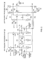
- Figure 2 depicts a CMOS implementation of the voltage translator depicted in Figure 1 ;
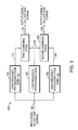
- Figure 3 depicts a block diagram a voltage translator according to another illustrative embodiment of the invention.
- Figure 4 depicts a CMOS implementation of the voltage translator depicted in Figure 2 ;
- Figure 5 depicts a merged BiCMOS implementation of the voltage translator depicted in Figure 1 ;
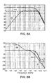
- Figure 6a depicts the magnitude of a frequency response of the BiCMOS implementation depicted in Figure 5 .
- Figure 6b depicts the phase of a frequency response of the BiCMOS implementation depicted in Figure 5 .
- the present invention pertains in various embodiments to voltage level translators and methods for translating signals from one voltage domain to another voltage domain.
- certain illustrative embodiments are described, including voltage level translators and methods for translating signals in, e.g. radio frequency (RF) range from about 10 MHz to about 5000 MHz, in an RF communication system.
- RF radio frequency
- FIG. 1 shows a block diagram of a voltage translator 100 according to an illustrative embodiment of the invention.
- the illustrated translator translates the signal voltage from an input voltage domain, V in , to an output voltage domain, V out .
- the translator 100 includes a low frequency processing stage 102 and a high frequency processing stage 104, both receiving the same input signal 106.
- the input signal 106 may be a single-ended signal or a differential signal. If the input signal is a single-ended signal, the input voltage domain, V in , is represented by the reference value of the input signal 106.
- V in is represented by the common mode voltage of the input signal 106, and in this case, as well known to a person skilled in the art, the input signal 106 will include two 180-degree phase-shifted signals, e.g. 106p, 106n.
- the low frequency processing stage 102 may be configured to process the input signal 106 to generate a signal 108 in a low frequency range.
- the reference voltage or the common mode voltage of the signal 108 does not determine the overall bandwidth of the translator, but is directly related to the voltage domain of the output signal of the translator 100. Accordingly, the signal 108 may have the reference voltage value (for the single-ended case) or the common mode voltage value (for the differential case) in the desired output voltage domain, V out .
- the high frequency processing stage 104 may be configured to process the input signal 106 to generate a signal 110 in a high frequency range.
- the reference voltage or the common mode voltage of the signal 110 does not contribute toward or is not relevant to the voltage domain of the output signal of the translator 100, but determines the overall bandwidth of the translator 100.
- the implementations of the stages 102, 104 may be chosen such that the translator 100 has favorable characteristics in terms of speed, breakdown voltages, power consumption, and size, for both low and high frequency ranges.
- the stage 104 is implemented without the use of passive components, or any slow or p-type devices.
- the low frequency processed signal 108 and the high frequency processed signal 110 are combined at a combining stage 112.
- the combining stage 112 combines the signals 108, 110 to produce an output signal 114, which collectively has the properties of the signals 108, 110.
- the output signal 114 has the reference voltage or the common mode voltage in the desired output voltage domain, V out , and also has the frequency range which covers the complete bandwidth of the translator 100.
- the values chosen for the components in the combining stage 112 determine the frequency (within the translator bandwidth) at which the low frequency processed signal 108 and the high frequency processed signal 110 are merged while still maintaining the integrity of the overall frequency response of the translator 100.
- Figure 2 shows a CMOS implementation of the embodiment of the translator 100 shown in Figure 1 , and accordingly, uses the same labels for the components shown in both Figures 1 and 2 . This implementation is shown and will be discussed with respect to differential signals.
- the low frequency processing stage 102 comprises a transconductance amplifier and two "folded" cascode amplifiers.
- the transconductance amplifier includes n-type field-effect transistors (FETs) T1 and T2, the gates of both of which receive input signals 106p, 106n.
- the input signals 106p, 106n have a phase difference of 180 degrees and together constitute the differential input signal 106 (which is in input voltage domain, V in ) of Figure 1 .
- the source of the transistor T1 is connected to a current source I1 which is connected to ground.
- the source of the transistor T2 is connected to a current source I2 which is connected to ground.
- a resistor R1 is connected at the top of the current sources I1, I2.
- the drain of the transistor T1 is connected to one end of a current source I3, the other end of which is connected to a voltage supply, Vdd.
- the drain of the transistor T2 is connected to one end of a current source I4, the other end of which is also connected to the voltage supply Vdd.
- the transconductance amplifier converts the input voltage signals 106p, 106n into respective current signals 206, 208 supplied at nodes 202, 204.
- one folded cascode amplifier of the low frequency processing stage 102 includes the transistor T1 and a p-type FET T3, and processes the current signal obtained from the difference of a current signal from I3 and the current signal 206.
- the other folded cascode amplifier includes the transistor T2 and a p-type FET T4, and processes the current signal obtained from the difference of a current signal from I4 and the current signal 208.
- the drain of the transistor T3 is connected at node 202, and the drain of the transistor T4 is connected at node 204.
- the gates of the transistors T3, T4 are connected to a biasing voltage source, Vcas, and their sources are connected to load resistors R2 and R3, respectively.
- the other ends of the resistors R2, R3 are commonly connected to the source of an n-type transistor T5, the gate of which is self-biased and the drain is connected to ground.
- Vcas is not greater than Vdd.
- the transistors T1, T2, T3, T4 operate in the input voltage domain, V in
- the transistor T5 operates in the output voltage domain, V out .
- the load resistors R2, R3, and the transistor T5 constitute a conversion stage to convert current signals from nodes 202, 204 into voltage signals 108p, 108n.
- the conversion stage may include other passive and active components connected in different topologies.
- the current signal from node 202 passes through the transistor T3, and is converted back to a voltage signal 108n at the resistor R2.
- the current signal from node 204 passes through the transistor T4, and is converted back to a voltage signal 108p at the resistor R3.
- the common mode voltage of the signals 108p, 108n is in the desired output voltage domain, V out , and is calculated as a sum of the voltage difference between the gate and source, V gs of T5 and the current value (at R2 or R3) times the resistance value (of R2 or R3).
- the voltage signals 108p, 108n may have the phase difference of 180 degrees and may be available at nodes 210, 212, respectively to be supplied to combining stages 112p, 112n.
- the high frequency processing stage 104 is implemented as a source-follower differential amplifier pair.
- This differential amplifier pair includes two n-type FETs T6, T7.
- the gates of the transistors T6, T7 receive the input signals 106p, 106n, the drains are commonly connected to the voltage supply Vdd, and the sources are connected to ground through current sources I5, I6.
- the transistors T6, T7 according to the voltage swing of the input signals 106p, 106n, the transistors T6, T7 generate outputs 110p, 110n at their respective sources, which are received at nodes 214, 216.
- the common mode voltage of the signals 110p, 110n may be less than Vdd, and not in the desired output voltage domain V out .
- the gain of the differential amplifier pair is gl, where g1 is desirably equal to one.
- g1 is desirably equal to one.
- a gain enhancement block 218 is connected at nodes 220, 222.
- the gain enhancement block 218 may include n-type FETs T8, T9, and a current source I7.
- the low frequency processed signal 108p is combined with the high frequency processed signal 110p at a combiner 112p.
- the low frequency processed signal 108n is combined with the high frequency processed signal 110n at a combiner 112n.
- the combiners 112p, 112n may be structurally similar or different. As shown in Figure 2 , both the combiners are the same and each includes a resistor and a capacitor.
- the combiner 112p includes a resistor R4 connected with a capacitor C1
- the combiner 112n includes a resistor R5 connected with a capacitor C2.
- the combiners 112p, 112n include passive networks comprising a resistor, a capacitor, and an inductor, or a capacitor and an inductor.
- the combiner 112p may act as a first-order low pass RC filter, and for the signal 110p at the node 212 arriving at the capacitor C1, the combiner 112p may serve as a first-order high pass CR filter.
- the cut-off frequency of both the low pass and the high pass filters is the same, and is calculated as the inverse of the product of the resistance of (R4+R3) and the capacitance of C1. Accordingly, the combination of the low-pass signal 108p and the high-pass signal 110p, in the frequency response sense, may be seamless.
- the signal 110p entering the CR high-pass filter is DC blocked due to the capacitor C1, while the rest of the frequencies are passed with different attenuations. Accordingly, the DC component of the signal 110p may not be related to the desired output voltage domain V out , and the signal 110p may determine the overall bandwidth of a translator 100. As discussed above, the signal 108p is in the output voltage domain V out , and hence, upon combination with the high-pass signal 110p, the combiner 112p generates an output signal 114p which is in the voltage domain V out , and has the frequency range equal to the bandwidth of the translator 100.
- the combiner 112n receives the low frequency processed signal 108n and act as a first-order low-pass filter for that signal, and receives the high frequency processed signal 110n at the node 216 and acts as a first-order high-pass filter for the signal 110n.
- the cut-off frequency of each of these filters is calculated as the inverse of the product of the resistance of (R5+R2) and the capacitance of C2, and this cut-off frequency may be different than the cut-off frequency of the filter of the combiner 112p.
- the combiner 112n combines the signals 108n and the signal 110 to generate an output signal 114n, and the common mode voltage of the signal 114n is, as desired, in the output voltage domain V out .
- FIG. 3 shows a block diagram of a voltage translator 100 according to another illustrative embodiment of the invention.
- the illustrated translator translates the signal voltage from an input voltage domain, V in , to an output voltage domain, V out .
- the translator 100 includes a low frequency processing stage 102, a high frequency processing stage 104 providing an overall gain gl, and a high frequency processing stage 302 with an overall gain g2.
- the high frequency processing stages 110, 304 are implemented differently to provide different gains.
- Such a translator implementation with multiple gains may be required as part of a programmable gain amplifier application for various communications and signal processing systems.
- all the stages receive the same input signal 106, which may be a single-ended signal or a differential signal.
- the low frequency processing stage 102 may be configured to process the input signal 106 and generate a signal 108 in a low frequency range.
- the reference voltage (for the single-ended case) or the common mode voltage (for the differential case) of the low frequency processed signal 108 is in the desired output voltage domain, V out .
- the high frequency processing stages 104, 302 may be configured to process the input signal 106 to generate signals 110, 304, respectively, in high frequency range.
- the signals 110, 304 determine the overall bandwidth of the translator.
- the low frequency processed signal 108 and the high frequency processed signal 110 are combined at a combining stage 112, and the signal 108 is also combined with the high frequency processed signal 304 at a combining stage 306.
- the combining stages 112, 306 may be structurally different to maintain the different gains from the high frequency processing stages 104, 302.
- the combining stages 112, 306 combine their respective input signals to generate output signals 114, 308.
- the signals 114, 308, each have the reference voltage or the common mode voltage in the desired output voltage domain, V out , and also have the frequency range which covers the complete bandwidth of the translator 100.
- Figure 4 shows the detailed CMOS implementation of an embodiment of the translator 100 shown in Figure 3 . This implementation is shown and will be discussed with respect to differential signals. In this implementation, the stages 102, 104 and the combiners 112p, 112n are structurally identical to those shown in Figure 2 .
- the implementation of the stage 302 is based on the implementation of the stage 104, i.e., including a source follower differential amplifier pair and a gain enhancement block.
- the differential input signals 106p, 106n may not be directly coupled to the gates of the transistor pair, as shown for the stage 104.
- the input signals 106p, 106n are fed to a voltage divider network including resistors R6, R7, R8. Capacitors C3, C4 may be connected in parallel to the resistors R6, R7, respectively, to pass the AC component and block the DC component of the input signals 106p, 106n which is processed through the divider network.
- the implementations of the combiners 306p, 306n are based on the implementations of the combiners 112p, 112n, i.e., each including a resistor and a capacitor, but further includes a voltage divider network comprising resistors R9, R10, R11 in accordance with the specific gain requirement of the stage 302.
- the divider network including R9, R10, R11 is connected with the low frequency processed signals 108p, 108n (which determine the voltage domain V out of the output signal).
- Output signals 308p, 308n from the combiners 306p, 306n may have the common mode voltage in the domain V out with gain equal to 1/2.
- FIG. 5 shows a merged BiCMOS implementation of an embodiment of the translator 100 shown in Figure 1 .
- bipolar junction transistors (BJTs) T1, T2 operate both as a transconductance amplifier for the low frequency processing stage 102, and as an emitter follower differential amplifier pair for the high frequency processing stage 104 of the translator 100.
- the bases of the transistors T1, T2 receive a differential signal including signals 106p, 106n with a common mode voltage in the input voltage domain V in .
- the outputs of the transconductance amplifier 108p, 108n may be received at nodes 502, 504 across resistors R1, R2 connected to the collectors of the transistors T1, T2.
- the outputs of the emitter follower differential amplifier pair 110p, 110n may be received at the emitters of the transistors T1, T2 through capacitors C1, C2.
- the signals 108p, 110p are combined at a combining stage comprising the resistor R1 and the capacitor C1 to generate an output signal 114p.
- the signals 108n, 110n are combined at a combining stage comprising the resistor R2 and the capacitor C2 to generate an output signal 114n.
- the common mode voltage of the output signals 114p, 114n may be in the output voltage domain V out .
- the translator 100 is powered between power supplies, Vdd and Vss, each of which may be a positive or a negative power supply.
- Figure 6a, 6b plot the magnitude and phase, respectively, of a frequency response of the BiCMOS implementation of Figure 5 .
- Plots 602, 604 show the magnitude and phase frequency responses of the output of the low frequency processing stage 102 (i.e., the transconductance amplifier)
- plots 606, 608 show the magnitude and phase frequency responses of the output of the high frequency processing stage 104 (i.e., the emitter follower differential amplifier)
- plots 610, 612 show the magnitude and phase frequency responses of the combined output.
Landscapes
- Engineering & Computer Science (AREA)
- Power Engineering (AREA)
- Amplifiers (AREA)
- Superheterodyne Receivers (AREA)
Abstract
Description
- The present application claims priority under 35 U.S.C. §119 from
U.S. Provisional Patent Application Ser. No. 61/174,689, filed on May 1, 2009 - The present invention relates generally to voltage translators used in integrated circuits (ICs), and more specifically, to wideband voltage translators used in high-speed ICs.
- In high-speed ICs, it is often necessary to drive signals, i.e. translate signal voltages, from one voltage domain to another (higher or lower) voltage domain. For example, in high-speed ICs, it may be required to translate signal voltages between an "I/O" voltage domain and a "core" voltage domain, or between a "clean" analog voltage domain and a "dirty" digital voltage domain. The signals to be translated may be single-ended signals or differential signals. In the case of single-ended signals, the voltage translation effectively changes the reference voltage of the signals of interest, and in the case of differential signals, the voltage translation alters the common mode voltage of the signals.
- Various implementations of a voltage translation circuit exist in the prior art; the following is a discussion of three conventional implementations. The first implementation translates signal voltage from an input voltage domain to an output voltage domain by using large series AC-coupling capacitors tied to large resistors. In effect, the capacitors block the DC components and pass the AC components of the signal, and generate the output signal in the output voltage domain. The resistors and capacitors in this implementation are required to be large to pass the low-frequency content without undesirable "droop" in the frequency response. However, the use of large resistors or large capacitors results in large circuit area and high cost, which are undesirable. In addition, the parasitic capacitance of the AC-coupling capacitor tends to negatively effect the high frequency performance of the circuit.
- The second implementation uses emitter followers or source followers to shift voltages between input and output domains, hence eliminating the need for large passive components, like in the first implementation, with minimal compromise of speed. However, this implementation does not readily allow an arbitrary shift in the voltage level of a signal, and particularly, with regard to differential signals, this implementation has an undesirable property that the output common mode voltage is proportional to the input common mode voltage.
- The third implementation employs a transconductance amplifier to convert the input voltage signal to a current signal that is delivered across the voltage domain boundary. At the output side of this implementation, either a resistive load or another transconductance stage may be used to convert the current signal back to a voltage signal. This approach also does not require large passive components, but is often much slower than the two above-discussed implementations because it often requires slower high-voltage devices or p-type devices in the signal path.
- In embodiments of the present invention, the problems of poor low-frequency response, slow speed, high cost and high power consumption in voltage translators are addressed by processing high frequency and low frequency components of an input signal separately in two parallel stages without the use of large passive components or slow devices. At the output, the processed high frequency and low frequency components are seamlessly merged at a combining stage that maintains the integrity of the frequency response over the complete translator bandwidth. In various embodiments, voltage translators and methods pertaining to this invention may be used in programmable gain amplifiers (PGAs) in an RF communication system operating over a wide range of frequencies.
- Accordingly, in one aspect, the invention pertains to a voltage level translator for translating an input signal in an input voltage domain to an output signal in an output voltage domain. The translator includes a low frequency stage, a high frequency stage, and a combining stage. The low frequency stage receives and processes the input signal to generate a first processed signal in a low frequency range, wherein the first processed signal is in the output voltage domain. The high frequency stage receives and processes the input signal to generate a second processed signal in a high frequency range, wherein the second processed signal determines a bandwidth of the translator. The combining stage combines the first and second processed signals to generate the output signal in the output voltage domain.
- In various embodiments, at least one of the input signal and the output signal is a single-ended signal or a differential signal.
- In various embodiments, the translator is implemented using CMOS or BiCMOS technology.
- In various embodiments, the low frequency stage includes a DC-coupled amplifier. In one embodiment, the DC-coupled amplifier includes a transconductance amplifier for converting the input voltage signal into a current signal. The DC-coupled amplifier may further comprise a conversion stage for receiving and converting the current signal into the first processed signal. In one embodiment, the DC-coupled amplifier further includes a cascode stage operatively connected between the transconductance amplifier and the conversion stage for transferring the current signal therebetween.
- In various embodiments, the high frequency stage comprises an AC-coupled amplifier. In one embodiment, the AC-coupled amplifier includes a source follower or an emitter follower amplifier for amplifying the input signal to generate the second processed signal. In another embodiment, the AC-coupled amplifier further includes a gain enhancement block.
- In one embodiment, the combining stage includes an RC, an LC or an RLC filter.
- In one embodiment, the low frequency and high frequency stages are implemented using the same transistors.
- In another aspect, the invention pertains to a method of translating an input signal in an input voltage domain to an output signal in an output voltage domain. The method includes receiving the input signal at a low frequency stage and at a high frequency stage. In one embodiment, at the low frequency stage, the input signal is processed to generate a first processed signal in a low frequency range, wherein the first processed signal is in the output voltage domain. At the high frequency stage, the input signal is processed to generate a second processed signal in a high frequency range, wherein the second processed signal determines a bandwidth of the translator. The method further includes combining the first and second processed signals at a combining stage to generate the output signal.
- In various embodiments, the method is used in a voltage level translation circuit which is implemented using CMOS or BiCMOS technology.
- In various embodiments, processing the input signal at the low frequency stage includes converting the input voltage signal into a current signal. In one embodiment, the processing at the low frequency stage further includes converting the current signal into the first processed signal.
- In various embodiments, processing the input signal at the high frequency stage includes amplifying the high frequency component of the input signal to generate the second processed signal.
- The foregoing and other features and advantages of the present invention will be made more apparent from the description, drawings, and claims that follow.
- In the drawings, like reference characters generally refer to the same parts throughout the different views. Also, the drawings are not necessarily to scale, emphasis instead generally being placed upon illustrating the principles of the invention. In the following description, various embodiments of the present invention are described with reference to the following drawings, in which:
-
Figure 1 depicts a block diagram of a voltage translator according to an illustrative embodiment of the invention; -
Figure 2 depicts a CMOS implementation of the voltage translator depicted inFigure 1 ; -
Figure 3 depicts a block diagram a voltage translator according to another illustrative embodiment of the invention; -
Figure 4 depicts a CMOS implementation of the voltage translator depicted inFigure 2 ; -
Figure 5 depicts a merged BiCMOS implementation of the voltage translator depicted inFigure 1 ; and -
Figure 6a depicts the magnitude of a frequency response of the BiCMOS implementation depicted inFigure 5 . -
Figure 6b depicts the phase of a frequency response of the BiCMOS implementation depicted inFigure 5 . - In general, the present invention pertains in various embodiments to voltage level translators and methods for translating signals from one voltage domain to another voltage domain. To provide an overall understanding of the invention, certain illustrative embodiments are described, including voltage level translators and methods for translating signals in, e.g. radio frequency (RF) range from about 10 MHz to about 5000 MHz, in an RF communication system.
-
Figure 1 shows a block diagram of avoltage translator 100 according to an illustrative embodiment of the invention. The illustrated translator translates the signal voltage from an input voltage domain, Vin, to an output voltage domain, Vout. Thetranslator 100 includes a lowfrequency processing stage 102 and a highfrequency processing stage 104, both receiving thesame input signal 106. Theinput signal 106 may be a single-ended signal or a differential signal. If the input signal is a single-ended signal, the input voltage domain, Vin, is represented by the reference value of theinput signal 106. Wheninput signal 106 is a differential signal, Vin is represented by the common mode voltage of theinput signal 106, and in this case, as well known to a person skilled in the art, theinput signal 106 will include two 180-degree phase-shifted signals, e.g. 106p, 106n. - The low
frequency processing stage 102 may be configured to process theinput signal 106 to generate asignal 108 in a low frequency range. In one embodiment, the reference voltage or the common mode voltage of thesignal 108 does not determine the overall bandwidth of the translator, but is directly related to the voltage domain of the output signal of thetranslator 100. Accordingly, thesignal 108 may have the reference voltage value (for the single-ended case) or the common mode voltage value (for the differential case) in the desired output voltage domain, Vout. - The high
frequency processing stage 104 may be configured to process theinput signal 106 to generate asignal 110 in a high frequency range. In one embodiment, the reference voltage or the common mode voltage of thesignal 110 does not contribute toward or is not relevant to the voltage domain of the output signal of thetranslator 100, but determines the overall bandwidth of thetranslator 100. Generally, the implementations of thestages translator 100 has favorable characteristics in terms of speed, breakdown voltages, power consumption, and size, for both low and high frequency ranges. For example, in one embodiment, thestage 104 is implemented without the use of passive components, or any slow or p-type devices. - In one embodiment, the low frequency processed
signal 108 and the high frequency processedsignal 110 are combined at a combiningstage 112. The combiningstage 112 combines thesignals output signal 114, which collectively has the properties of thesignals output signal 114 has the reference voltage or the common mode voltage in the desired output voltage domain, Vout, and also has the frequency range which covers the complete bandwidth of thetranslator 100. In one embodiment, the values chosen for the components in the combiningstage 112 determine the frequency (within the translator bandwidth) at which the low frequency processedsignal 108 and the high frequency processedsignal 110 are merged while still maintaining the integrity of the overall frequency response of thetranslator 100. -
Figure 2 shows a CMOS implementation of the embodiment of thetranslator 100 shown inFigure 1 , and accordingly, uses the same labels for the components shown in bothFigures 1 and2 . This implementation is shown and will be discussed with respect to differential signals. - In this embodiment, the low
frequency processing stage 102 comprises a transconductance amplifier and two "folded" cascode amplifiers. In one embodiment, the transconductance amplifier includes n-type field-effect transistors (FETs) T1 and T2, the gates of both of which receiveinput signals Figure 1 . The source of the transistor T1 is connected to a current source I1 which is connected to ground. Similarly, the source of the transistor T2 is connected to a current source I2 which is connected to ground. A resistor R1 is connected at the top of the current sources I1, I2. Atnode 202, the drain of the transistor T1 is connected to one end of a current source I3, the other end of which is connected to a voltage supply, Vdd. Similarly, atnode 204, the drain of the transistor T2 is connected to one end of a current source I4, the other end of which is also connected to the voltage supply Vdd. In this embodiment, the transconductance amplifier converts theinput voltage signals current signals nodes - In one embodiment, one folded cascode amplifier of the low
frequency processing stage 102 includes the transistor T1 and a p-type FET T3, and processes the current signal obtained from the difference of a current signal from I3 and thecurrent signal 206. The other folded cascode amplifier includes the transistor T2 and a p-type FET T4, and processes the current signal obtained from the difference of a current signal from I4 and thecurrent signal 208. The drain of the transistor T3 is connected atnode 202, and the drain of the transistor T4 is connected atnode 204. The gates of the transistors T3, T4 are connected to a biasing voltage source, Vcas, and their sources are connected to load resistors R2 and R3, respectively. The other ends of the resistors R2, R3 are commonly connected to the source of an n-type transistor T5, the gate of which is self-biased and the drain is connected to ground. In one embodiment, Vcas is not greater than Vdd. In one embodiment, the transistors T1, T2, T3, T4 operate in the input voltage domain, Vin, and the transistor T5 operates in the output voltage domain, Vout. In one embodiment, the load resistors R2, R3, and the transistor T5 constitute a conversion stage to convert current signals fromnodes voltage signals - The current signal from
node 202 passes through the transistor T3, and is converted back to avoltage signal 108n at the resistor R2. Similarly, the current signal fromnode 204 passes through the transistor T4, and is converted back to avoltage signal 108p at the resistor R3. In one embodiment, the common mode voltage of thesignals nodes stages - Still referring to
Figure 2 , in one embodiment, the highfrequency processing stage 104 is implemented as a source-follower differential amplifier pair. This differential amplifier pair includes two n-type FETs T6, T7. The gates of the transistors T6, T7 receive the input signals 106p, 106n, the drains are commonly connected to the voltage supply Vdd, and the sources are connected to ground through current sources I5, I6. In one embodiment, according to the voltage swing of the input signals 106p, 106n, the transistors T6, T7 generateoutputs nodes 214, 216. The common mode voltage of thesignals gain enhancement block 218 is connected atnodes gain enhancement block 218 may include n-type FETs T8, T9, and a current source I7. - In one embodiment, the low frequency processed
signal 108p is combined with the high frequency processedsignal 110p at acombiner 112p. Similarly, the low frequency processedsignal 108n is combined with the high frequency processedsignal 110n at acombiner 112n. Thecombiners Figure 2 , both the combiners are the same and each includes a resistor and a capacitor. Thecombiner 112p includes a resistor R4 connected with a capacitor C1, and thecombiner 112n includes a resistor R5 connected with a capacitor C2. In another embodiment, thecombiners - For the
signal 108p coming in at the resistor R4, thecombiner 112p may act as a first-order low pass RC filter, and for thesignal 110p at thenode 212 arriving at the capacitor C1, thecombiner 112p may serve as a first-order high pass CR filter. The cut-off frequency of both the low pass and the high pass filters is the same, and is calculated as the inverse of the product of the resistance of (R4+R3) and the capacitance of C1. Accordingly, the combination of the low-pass signal 108p and the high-pass signal 110p, in the frequency response sense, may be seamless. - The
signal 110p entering the CR high-pass filter is DC blocked due to the capacitor C1, while the rest of the frequencies are passed with different attenuations. Accordingly, the DC component of thesignal 110p may not be related to the desired output voltage domain Vout, and thesignal 110p may determine the overall bandwidth of atranslator 100. As discussed above, thesignal 108p is in the output voltage domain Vout, and hence, upon combination with the high-pass signal 110p, thecombiner 112p generates anoutput signal 114p which is in the voltage domain Vout, and has the frequency range equal to the bandwidth of thetranslator 100. - Similar to the operation of the
combiner 112p, thecombiner 112n receives the low frequency processedsignal 108n and act as a first-order low-pass filter for that signal, and receives the high frequency processedsignal 110n at thenode 216 and acts as a first-order high-pass filter for thesignal 110n. The cut-off frequency of each of these filters is calculated as the inverse of the product of the resistance of (R5+R2) and the capacitance of C2, and this cut-off frequency may be different than the cut-off frequency of the filter of thecombiner 112p. Thecombiner 112n combines thesignals 108n and thesignal 110 to generate anoutput signal 114n, and the common mode voltage of thesignal 114n is, as desired, in the output voltage domain Vout. -
Figure 3 shows a block diagram of avoltage translator 100 according to another illustrative embodiment of the invention. The illustrated translator translates the signal voltage from an input voltage domain, Vin, to an output voltage domain, Vout. Thetranslator 100 includes a lowfrequency processing stage 102, a highfrequency processing stage 104 providing an overall gain gl, and a highfrequency processing stage 302 with an overall gain g2. In one embodiment, there is only one lowfrequency processing stage 102 required to work in parallel with one or more high frequency processing stages, e.g., stages 104, 302. In another embodiment, the high frequency processing stages 110, 304 are implemented differently to provide different gains. Such a translator implementation with multiple gains may be required as part of a programmable gain amplifier application for various communications and signal processing systems. - In this embodiment, all the stages receive the
same input signal 106, which may be a single-ended signal or a differential signal. The lowfrequency processing stage 102 may be configured to process theinput signal 106 and generate asignal 108 in a low frequency range. In one embodiment, the reference voltage (for the single-ended case) or the common mode voltage (for the differential case) of the low frequency processedsignal 108 is in the desired output voltage domain, Vout. The high frequency processing stages 104, 302 may be configured to process theinput signal 106 to generatesignals signals - In one embodiment, the low frequency processed
signal 108 and the high frequency processedsignal 110 are combined at a combiningstage 112, and thesignal 108 is also combined with the high frequency processedsignal 304 at a combiningstage 306. The combiningstages stages output signals signals translator 100. -
Figure 4 shows the detailed CMOS implementation of an embodiment of thetranslator 100 shown inFigure 3 . This implementation is shown and will be discussed with respect to differential signals. In this implementation, thestages combiners Figure 2 . - In this implementation, the high
frequency processing stage 104 provides unity gain, i.e., g1=1, and the highfrequency processing stage 302 provides gain, g2 = 1/2. In one embodiment, the implementation of thestage 302 is based on the implementation of thestage 104, i.e., including a source follower differential amplifier pair and a gain enhancement block. However, to provide a gain of 1/2 at the output, thedifferential input signals stage 104. In one embodiment, the input signals 106p, 106n are fed to a voltage divider network including resistors R6, R7, R8. Capacitors C3, C4 may be connected in parallel to the resistors R6, R7, respectively, to pass the AC component and block the DC component of the input signals 106p, 106n which is processed through the divider network. - In one embodiment, the implementations of the
combiners combiners stage 302. The divider network including R9, R10, R11 is connected with the low frequency processedsignals Output signals combiners -
Figure 5 shows a merged BiCMOS implementation of an embodiment of thetranslator 100 shown inFigure 1 . In this implementation, bipolar junction transistors (BJTs) T1, T2 operate both as a transconductance amplifier for the lowfrequency processing stage 102, and as an emitter follower differential amplifier pair for the highfrequency processing stage 104 of thetranslator 100. The bases of the transistors T1, T2 receive a differentialsignal including signals transconductance amplifier nodes differential amplifier pair signals output signal 114p. In another embodiment, thesignals output signal 114n. The common mode voltage of theoutput signals - In various embodiments, the
translator 100 is powered between power supplies, Vdd and Vss, each of which may be a positive or a negative power supply. -
Figure 6a, 6b plot the magnitude and phase, respectively, of a frequency response of the BiCMOS implementation ofFigure 5 .Plots - It will therefore be seen that the foregoing represents a highly advantageous approach to translate signal voltage between different voltage domains in high-speed ICs. The terms and expressions employed herein are used as terms of description and not of limitation and there is no intention, in the use of such terms and expressions, of excluding any equivalents of the features shown and described or portions thereof, but it is recognized that various modifications are possible within the scope of the invention claims.
Claims (15)
- A voltage level translator for translating an input signal in an input voltage domain to an output signal in an output voltage domain, the translator comprising:a low frequency stage (102) for receiving and processing the input signal to generate a first processed signal in a low frequency range, wherein the first processed signal is in the output voltage domain;a high frequency stage (104) for receiving and processing the input signal to generate a second processed signal in a high frequency range, wherein the second processed signal determines a bandwidth of the translator; anda combining stage for combining the first and second processed signals to generate the output signal.
- The voltage level translator of claim 1, wherein one or more of the following applies:1) at least one of the input signal and the output signal is a single-ended signal or a differential signal:2) the translator is implemented using CMOS or BiCMOS technology.
- The voltage level translator of any of the preceding claims, wherein the low frequency stage comprises a DC-coupled amplifier.
- The voltage translator of claim 3, wherein the DC-coupled amplifier comprises a transconductance amplifier for converting the input voltage signal into a current signal.
- The voltage translator of claim 4, wherein the DC-coupled amplifier further comprises a conversion stage for receiving and converting the current signal into the first processed signal.
- The voltage translator of claim 5, wherein the DC-coupled amplifier further comprises a cascode stage operatively connected between the transconductance amplifier and the conversion stage for transferring the current signal therebetween.
- The voltage level translator as claimed in any of the preceding claims, wherein the high frequency stage comprises an AC-coupled amplifier.
- The voltage level translator of claim 7, wherein one or more of the following conditions apply:1) the AC-coupled amplifier comprises a source follower or an emitter follower amplifier for amplifying the input signal to generate the second processed signal;2) the AC-coupled amplifier further comprises a gain enhancement block.
- The voltage level translator as claimed in any of the preceding claims, wherein the combining stage comprises an RC, an LC or an RLC filter.
- The voltage level translator as claimed in any of the preceding claims, wherein the low frequency and high frequency stages are implemented using the same transistors.
- A method of translating an input signal in an input voltage domain to an output signal in an output voltage domain, the method comprising:receiving and processing the input signal at a low frequency stage to generate a first processed signal in a low frequency range, wherein the first processed signal is in the output voltage domain;receiving and processing the input signal at a high frequency stage to generate a second processed signal in a high frequency range, wherein the second processed signal determines a bandwidth of the translator; andcombining the first and second processed signals at a combining stage to generate the output signal.
- The method of claim 11, wherein at least one of the following conditions apply:1) at least one of the input signal and the output signal is a single-ended signal or differential signal;2) the method is used in a voltage level translation circuit which is implemented using CMOS or BiCMOS technology;3) processing the input signal at the high frequency stage comprises amplifying the high frequency component of the input signal to generate the second processed signal;4) the combining stage comprises an RC, an LC or an RLC filter.
- The method of claim 11 or 12, wherein processing the input signal at the low frequency stage comprises converting the input voltage signal into a current signal .
- The method of claim 13, wherein processing the input signal at the low frequency stage further comprises converting the current signal into the first processed signal.
- The method of claim 11, 12, 13 or 14 wherein the low frequency and high frequency stages are implemented using the same transistors.
Applications Claiming Priority (1)
| Application Number | Priority Date | Filing Date | Title |
|---|---|---|---|
| US17468909P | 2009-05-01 | 2009-05-01 |
Publications (3)
| Publication Number | Publication Date |
|---|---|
| EP2246977A2 true EP2246977A2 (en) | 2010-11-03 |
| EP2246977A3 EP2246977A3 (en) | 2012-11-14 |
| EP2246977B1 EP2246977B1 (en) | 2017-05-24 |
Family
ID=42320668
Family Applications (1)
| Application Number | Title | Priority Date | Filing Date |
|---|---|---|---|
| EP10161454.3A Not-in-force EP2246977B1 (en) | 2009-05-01 | 2010-04-29 | Wideband voltage translators |
Country Status (3)
| Country | Link |
|---|---|
| US (1) | US8106700B2 (en) |
| EP (1) | EP2246977B1 (en) |
| CN (1) | CN101877537B (en) |
Cited By (2)
| Publication number | Priority date | Publication date | Assignee | Title |
|---|---|---|---|---|
| EP3371891A4 (en) * | 2015-11-05 | 2019-06-26 | Adtran, Inc. | SYSTEMS AND METHODS FOR HIGH SPEED SIGNAL COMMUNICATION IN A COMMUNICATION DEVICE |
| US10944599B2 (en) | 2019-06-28 | 2021-03-09 | Adtran, Inc. | Systems and methods for communicating high speed signals in a communication device |
Families Citing this family (12)
| Publication number | Priority date | Publication date | Assignee | Title |
|---|---|---|---|---|
| US20120235729A1 (en) * | 2011-03-15 | 2012-09-20 | Stmicroelectronics S.R.L. | Integrated device and method of reducing voltage drops on a supply distribution metal path of a device |
| US8718127B2 (en) | 2011-08-02 | 2014-05-06 | Analog Devices, Inc. | Apparatus and method for digitally-controlled adaptive equalizer |
| US8558613B2 (en) | 2011-08-02 | 2013-10-15 | Analog Devices, Inc. | Apparatus and method for digitally-controlled automatic gain amplification |
| US8847687B2 (en) | 2012-03-26 | 2014-09-30 | Agilent Technologies, Inc. | Multi-path broadband amplifier |
| CN103490765B (en) * | 2013-09-26 | 2016-03-30 | 华为技术有限公司 | Common mode electrical level stabilizing circuit |
| US9548739B2 (en) * | 2015-03-27 | 2017-01-17 | Qualcomm Incorporated | Drive for cascode stack of power FETs |
| US10397027B2 (en) * | 2017-09-26 | 2019-08-27 | International Business Machines Corporation | Continuous time linear equalizer |
| CN109000741B (en) * | 2018-06-06 | 2019-12-27 | 胡国勇 | Voltage data acquisition device and method for fire prevention and control in fire safety scientific engineering |
| US10541675B1 (en) * | 2018-11-15 | 2020-01-21 | King Fahd University Of Petroleum And Minerals | Multi-gain transconductance amplifier |
| US11349576B2 (en) * | 2019-06-28 | 2022-05-31 | Adtran, Inc. | Systems and methods for communicating high speed signals in a communication device |
| US11125817B2 (en) * | 2019-10-14 | 2021-09-21 | Analog Devices, Inc. | Compound pin driver |
| US11824530B2 (en) * | 2021-08-03 | 2023-11-21 | AyDeeKay LLC | Low latency, broadband power-domain offset-correction signal level circuit implementation |
Family Cites Families (18)
| Publication number | Priority date | Publication date | Assignee | Title |
|---|---|---|---|---|
| JPH04129309A (en) * | 1990-09-19 | 1992-04-30 | Matsushita Electric Ind Co Ltd | amplifier circuit |
| JPH0774616A (en) | 1993-07-06 | 1995-03-17 | Seiko Epson Corp | Signal voltage level conversion circuit and output buffer circuit |
| JP3689197B2 (en) * | 1996-09-06 | 2005-08-31 | 三菱電機株式会社 | Level shift circuit |
| US6084468A (en) * | 1997-10-06 | 2000-07-04 | Motorola, Inc. | Method and apparatus for high efficiency wideband power amplification |
| EP0930802B1 (en) | 1997-12-19 | 2008-09-03 | Texas Instruments Inc. | Microphone bias current measurement circuit |
| US6211732B1 (en) * | 1998-03-12 | 2001-04-03 | Sentel Corporation | Comb linear amplifier combiner (CLAC) |
| US6282146B1 (en) | 1999-06-21 | 2001-08-28 | Rise Technology, Inc. | Dual supply voltage input/output buffer |
| US6275112B1 (en) | 1999-10-28 | 2001-08-14 | Texas Instruments Incorporated | Efficient microphone bias amplifier with high output voltage/current capability and excellent PSRR |
| US6803801B2 (en) | 2002-11-07 | 2004-10-12 | Lsi Logic Corporation | CMOS level shifters using native devices |
| JP3989358B2 (en) * | 2002-11-13 | 2007-10-10 | 株式会社日立製作所 | Semiconductor integrated circuit device and electronic system |
| US6774698B1 (en) | 2003-01-30 | 2004-08-10 | Agere Systems Inc. | Voltage translator circuit for a mixed voltage circuit |
| US7068091B1 (en) | 2003-02-27 | 2006-06-27 | Cypress Semiconductor Corporation | Voltage translator circuit formed using low voltage transistors |
| KR100724559B1 (en) | 2004-12-15 | 2007-06-04 | 삼성전자주식회사 | Level shifter |
| KR100667303B1 (en) * | 2005-02-01 | 2007-01-12 | 삼성전자주식회사 | LNA for home use |
| JP2009533950A (en) * | 2006-04-12 | 2009-09-17 | トムソン ライセンシング | Active splitter apparatus and method using diplex front end |
| US7710152B1 (en) | 2006-07-07 | 2010-05-04 | Analog Devices, Inc. | Multistage dual logic level voltage translator |
| JP4935294B2 (en) | 2006-10-18 | 2012-05-23 | 富士電機株式会社 | Insulated gate device drive circuit |
| US7554379B2 (en) | 2007-02-23 | 2009-06-30 | Integrated Device Technology, Inc. | High-speed, low-power level shifter for mixed signal-level environments |
-
2009
- 2009-07-15 US US12/503,372 patent/US8106700B2/en active Active
-
2010
- 2010-04-29 EP EP10161454.3A patent/EP2246977B1/en not_active Not-in-force
- 2010-04-29 CN CN201010199598.3A patent/CN101877537B/en not_active Expired - Fee Related
Cited By (2)
| Publication number | Priority date | Publication date | Assignee | Title |
|---|---|---|---|---|
| EP3371891A4 (en) * | 2015-11-05 | 2019-06-26 | Adtran, Inc. | SYSTEMS AND METHODS FOR HIGH SPEED SIGNAL COMMUNICATION IN A COMMUNICATION DEVICE |
| US10944599B2 (en) | 2019-06-28 | 2021-03-09 | Adtran, Inc. | Systems and methods for communicating high speed signals in a communication device |
Also Published As
| Publication number | Publication date |
|---|---|
| EP2246977A3 (en) | 2012-11-14 |
| US8106700B2 (en) | 2012-01-31 |
| EP2246977B1 (en) | 2017-05-24 |
| US20100277215A1 (en) | 2010-11-04 |
| CN101877537A (en) | 2010-11-03 |
| CN101877537B (en) | 2014-07-16 |
Similar Documents
| Publication | Publication Date | Title |
|---|---|---|
| US8106700B2 (en) | Wideband voltage translators | |
| CN103219961B (en) | An Operational Amplifier Circuit with Adjustable Bandwidth | |
| US8487695B2 (en) | Differential source follower having 6dB gain with applications to WiGig baseband filters | |
| WO2017160747A1 (en) | Active linearization for broadband amplifiers | |
| EP3272007B1 (en) | Amplifier adapted for noise suppression | |
| US6396352B1 (en) | CMOS power amplifier for driving low impedance loads | |
| TWI548205B (en) | Balanced upscale mixer | |
| Wan et al. | A complementary current-mirror-based bulk-driven down-conversion mixer for wideband applications | |
| US6980055B2 (en) | CMOS differential buffer circuit | |
| KR19980036295A (en) | Mixers with Replication Voltage-to-Current Converter | |
| JPH07131256A (en) | Electronic circuit | |
| US6400219B1 (en) | High-speed offset comparator | |
| CN104956589A (en) | Improved RF Low Noise Amplifier Load Circuit | |
| CN113872531A (en) | Push-pull power amplifying circuit and radio frequency front end module | |
| US6664842B1 (en) | FET active load and current source | |
| JP2015170892A (en) | Low noise amplifier circuit | |
| US8803609B2 (en) | Bandwidth extension of an amplifier | |
| JP6416020B2 (en) | Active load circuit and semiconductor integrated circuit | |
| Acosta et al. | A simple approach for the implementation of CMOS amplifiers with constant bandwidth independent of gain | |
| JP2012099915A (en) | Wideband amplifier | |
| US20080265992A1 (en) | Transconductance Stage Arrangement | |
| JP5205403B2 (en) | Semiconductor integrated circuit device | |
| Muñiz-Montero et al. | A 90µm× 64µm225μW class-AB CMOS differential flipped voltage follower with output driving capability up to 100 pF | |
| Rezaei | A new active resistor and its application to a CMOS transconductor | |
| US20150372844A1 (en) | Wideband Parasitic Capacitance Cancellation for High Speed Switches in Serial Communication |
Legal Events
| Date | Code | Title | Description |
|---|---|---|---|
| PUAI | Public reference made under article 153(3) epc to a published international application that has entered the european phase |
Free format text: ORIGINAL CODE: 0009012 |
|
| AK | Designated contracting states |
Kind code of ref document: A2 Designated state(s): AT BE BG CH CY CZ DE DK EE ES FI FR GB GR HR HU IE IS IT LI LT LU LV MC MK MT NL NO PL PT RO SE SI SK SM TR |
|
| AX | Request for extension of the european patent |
Extension state: AL BA ME RS |
|
| PUAL | Search report despatched |
Free format text: ORIGINAL CODE: 0009013 |
|
| AK | Designated contracting states |
Kind code of ref document: A3 Designated state(s): AT BE BG CH CY CZ DE DK EE ES FI FR GB GR HR HU IE IS IT LI LT LU LV MC MK MT NL NO PL PT RO SE SI SK SM TR |
|
| AX | Request for extension of the european patent |
Extension state: AL BA ME RS |
|
| RIC1 | Information provided on ipc code assigned before grant |
Ipc: H03F 3/45 20060101ALI20121011BHEP Ipc: H03F 3/50 20060101AFI20121011BHEP Ipc: H03F 3/21 20060101ALI20121011BHEP Ipc: H03F 1/02 20060101ALI20121011BHEP Ipc: H03F 3/72 20060101ALI20121011BHEP |
|
| 17P | Request for examination filed |
Effective date: 20121213 |
|
| 17Q | First examination report despatched |
Effective date: 20130208 |
|
| GRAP | Despatch of communication of intention to grant a patent |
Free format text: ORIGINAL CODE: EPIDOSNIGR1 |
|
| INTG | Intention to grant announced |
Effective date: 20161222 |
|
| GRAS | Grant fee paid |
Free format text: ORIGINAL CODE: EPIDOSNIGR3 |
|
| GRAA | (expected) grant |
Free format text: ORIGINAL CODE: 0009210 |
|
| AK | Designated contracting states |
Kind code of ref document: B1 Designated state(s): AT BE BG CH CY CZ DE DK EE ES FI FR GB GR HR HU IE IS IT LI LT LU LV MC MK MT NL NO PL PT RO SE SI SK SM TR |
|
| REG | Reference to a national code |
Ref country code: GB Ref legal event code: FG4D |
|
| REG | Reference to a national code |
Ref country code: CH Ref legal event code: EP |
|
| REG | Reference to a national code |
Ref country code: IE Ref legal event code: FG4D |
|
| REG | Reference to a national code |
Ref country code: AT Ref legal event code: REF Ref document number: 896455 Country of ref document: AT Kind code of ref document: T Effective date: 20170615 |
|
| REG | Reference to a national code |
Ref country code: DE Ref legal event code: R096 Ref document number: 602010042519 Country of ref document: DE |
|
| REG | Reference to a national code |
Ref country code: NL Ref legal event code: MP Effective date: 20170524 |
|
| REG | Reference to a national code |
Ref country code: LT Ref legal event code: MG4D |
|
| REG | Reference to a national code |
Ref country code: AT Ref legal event code: MK05 Ref document number: 896455 Country of ref document: AT Kind code of ref document: T Effective date: 20170524 |
|
| PG25 | Lapsed in a contracting state [announced via postgrant information from national office to epo] |
Ref country code: GR Free format text: LAPSE BECAUSE OF FAILURE TO SUBMIT A TRANSLATION OF THE DESCRIPTION OR TO PAY THE FEE WITHIN THE PRESCRIBED TIME-LIMIT Effective date: 20170825 Ref country code: AT Free format text: LAPSE BECAUSE OF FAILURE TO SUBMIT A TRANSLATION OF THE DESCRIPTION OR TO PAY THE FEE WITHIN THE PRESCRIBED TIME-LIMIT Effective date: 20170524 Ref country code: ES Free format text: LAPSE BECAUSE OF FAILURE TO SUBMIT A TRANSLATION OF THE DESCRIPTION OR TO PAY THE FEE WITHIN THE PRESCRIBED TIME-LIMIT Effective date: 20170524 Ref country code: NO Free format text: LAPSE BECAUSE OF FAILURE TO SUBMIT A TRANSLATION OF THE DESCRIPTION OR TO PAY THE FEE WITHIN THE PRESCRIBED TIME-LIMIT Effective date: 20170824 Ref country code: HR Free format text: LAPSE BECAUSE OF FAILURE TO SUBMIT A TRANSLATION OF THE DESCRIPTION OR TO PAY THE FEE WITHIN THE PRESCRIBED TIME-LIMIT Effective date: 20170524 Ref country code: FI Free format text: LAPSE BECAUSE OF FAILURE TO SUBMIT A TRANSLATION OF THE DESCRIPTION OR TO PAY THE FEE WITHIN THE PRESCRIBED TIME-LIMIT Effective date: 20170524 Ref country code: LT Free format text: LAPSE BECAUSE OF FAILURE TO SUBMIT A TRANSLATION OF THE DESCRIPTION OR TO PAY THE FEE WITHIN THE PRESCRIBED TIME-LIMIT Effective date: 20170524 |
|
| PG25 | Lapsed in a contracting state [announced via postgrant information from national office to epo] |
Ref country code: SE Free format text: LAPSE BECAUSE OF FAILURE TO SUBMIT A TRANSLATION OF THE DESCRIPTION OR TO PAY THE FEE WITHIN THE PRESCRIBED TIME-LIMIT Effective date: 20170524 Ref country code: LV Free format text: LAPSE BECAUSE OF FAILURE TO SUBMIT A TRANSLATION OF THE DESCRIPTION OR TO PAY THE FEE WITHIN THE PRESCRIBED TIME-LIMIT Effective date: 20170524 Ref country code: IS Free format text: LAPSE BECAUSE OF FAILURE TO SUBMIT A TRANSLATION OF THE DESCRIPTION OR TO PAY THE FEE WITHIN THE PRESCRIBED TIME-LIMIT Effective date: 20170924 Ref country code: NL Free format text: LAPSE BECAUSE OF FAILURE TO SUBMIT A TRANSLATION OF THE DESCRIPTION OR TO PAY THE FEE WITHIN THE PRESCRIBED TIME-LIMIT Effective date: 20170524 Ref country code: BG Free format text: LAPSE BECAUSE OF FAILURE TO SUBMIT A TRANSLATION OF THE DESCRIPTION OR TO PAY THE FEE WITHIN THE PRESCRIBED TIME-LIMIT Effective date: 20170824 |
|
| PG25 | Lapsed in a contracting state [announced via postgrant information from national office to epo] |
Ref country code: RO Free format text: LAPSE BECAUSE OF FAILURE TO SUBMIT A TRANSLATION OF THE DESCRIPTION OR TO PAY THE FEE WITHIN THE PRESCRIBED TIME-LIMIT Effective date: 20170524 Ref country code: DK Free format text: LAPSE BECAUSE OF FAILURE TO SUBMIT A TRANSLATION OF THE DESCRIPTION OR TO PAY THE FEE WITHIN THE PRESCRIBED TIME-LIMIT Effective date: 20170524 Ref country code: CZ Free format text: LAPSE BECAUSE OF FAILURE TO SUBMIT A TRANSLATION OF THE DESCRIPTION OR TO PAY THE FEE WITHIN THE PRESCRIBED TIME-LIMIT Effective date: 20170524 Ref country code: EE Free format text: LAPSE BECAUSE OF FAILURE TO SUBMIT A TRANSLATION OF THE DESCRIPTION OR TO PAY THE FEE WITHIN THE PRESCRIBED TIME-LIMIT Effective date: 20170524 Ref country code: SK Free format text: LAPSE BECAUSE OF FAILURE TO SUBMIT A TRANSLATION OF THE DESCRIPTION OR TO PAY THE FEE WITHIN THE PRESCRIBED TIME-LIMIT Effective date: 20170524 |
|
| REG | Reference to a national code |
Ref country code: DE Ref legal event code: R097 Ref document number: 602010042519 Country of ref document: DE |
|
| PG25 | Lapsed in a contracting state [announced via postgrant information from national office to epo] |
Ref country code: IT Free format text: LAPSE BECAUSE OF FAILURE TO SUBMIT A TRANSLATION OF THE DESCRIPTION OR TO PAY THE FEE WITHIN THE PRESCRIBED TIME-LIMIT Effective date: 20170524 Ref country code: SM Free format text: LAPSE BECAUSE OF FAILURE TO SUBMIT A TRANSLATION OF THE DESCRIPTION OR TO PAY THE FEE WITHIN THE PRESCRIBED TIME-LIMIT Effective date: 20170524 Ref country code: PL Free format text: LAPSE BECAUSE OF FAILURE TO SUBMIT A TRANSLATION OF THE DESCRIPTION OR TO PAY THE FEE WITHIN THE PRESCRIBED TIME-LIMIT Effective date: 20170524 |
|
| PLBE | No opposition filed within time limit |
Free format text: ORIGINAL CODE: 0009261 |
|
| STAA | Information on the status of an ep patent application or granted ep patent |
Free format text: STATUS: NO OPPOSITION FILED WITHIN TIME LIMIT |
|
| 26N | No opposition filed |
Effective date: 20180227 |
|
| PG25 | Lapsed in a contracting state [announced via postgrant information from national office to epo] |
Ref country code: SI Free format text: LAPSE BECAUSE OF FAILURE TO SUBMIT A TRANSLATION OF THE DESCRIPTION OR TO PAY THE FEE WITHIN THE PRESCRIBED TIME-LIMIT Effective date: 20170524 |
|
| PG25 | Lapsed in a contracting state [announced via postgrant information from national office to epo] |
Ref country code: MC Free format text: LAPSE BECAUSE OF FAILURE TO SUBMIT A TRANSLATION OF THE DESCRIPTION OR TO PAY THE FEE WITHIN THE PRESCRIBED TIME-LIMIT Effective date: 20170524 |
|
| REG | Reference to a national code |
Ref country code: CH Ref legal event code: PL |
|
| REG | Reference to a national code |
Ref country code: BE Ref legal event code: MM Effective date: 20180430 |
|
| REG | Reference to a national code |
Ref country code: IE Ref legal event code: MM4A |
|
| PG25 | Lapsed in a contracting state [announced via postgrant information from national office to epo] |
Ref country code: LU Free format text: LAPSE BECAUSE OF NON-PAYMENT OF DUE FEES Effective date: 20180429 |
|
| PG25 | Lapsed in a contracting state [announced via postgrant information from national office to epo] |
Ref country code: CH Free format text: LAPSE BECAUSE OF NON-PAYMENT OF DUE FEES Effective date: 20180430 Ref country code: LI Free format text: LAPSE BECAUSE OF NON-PAYMENT OF DUE FEES Effective date: 20180430 Ref country code: BE Free format text: LAPSE BECAUSE OF NON-PAYMENT OF DUE FEES Effective date: 20180430 |
|
| PG25 | Lapsed in a contracting state [announced via postgrant information from national office to epo] |
Ref country code: IE Free format text: LAPSE BECAUSE OF NON-PAYMENT OF DUE FEES Effective date: 20180429 Ref country code: FR Free format text: LAPSE BECAUSE OF NON-PAYMENT OF DUE FEES Effective date: 20180430 |
|
| PG25 | Lapsed in a contracting state [announced via postgrant information from national office to epo] |
Ref country code: MT Free format text: LAPSE BECAUSE OF NON-PAYMENT OF DUE FEES Effective date: 20180429 |
|
| PG25 | Lapsed in a contracting state [announced via postgrant information from national office to epo] |
Ref country code: TR Free format text: LAPSE BECAUSE OF FAILURE TO SUBMIT A TRANSLATION OF THE DESCRIPTION OR TO PAY THE FEE WITHIN THE PRESCRIBED TIME-LIMIT Effective date: 20170524 |
|
| PG25 | Lapsed in a contracting state [announced via postgrant information from national office to epo] |
Ref country code: HU Free format text: LAPSE BECAUSE OF FAILURE TO SUBMIT A TRANSLATION OF THE DESCRIPTION OR TO PAY THE FEE WITHIN THE PRESCRIBED TIME-LIMIT; INVALID AB INITIO Effective date: 20100429 Ref country code: PT Free format text: LAPSE BECAUSE OF FAILURE TO SUBMIT A TRANSLATION OF THE DESCRIPTION OR TO PAY THE FEE WITHIN THE PRESCRIBED TIME-LIMIT Effective date: 20170524 |
|
| PG25 | Lapsed in a contracting state [announced via postgrant information from national office to epo] |
Ref country code: MK Free format text: LAPSE BECAUSE OF NON-PAYMENT OF DUE FEES Effective date: 20170524 Ref country code: CY Free format text: LAPSE BECAUSE OF FAILURE TO SUBMIT A TRANSLATION OF THE DESCRIPTION OR TO PAY THE FEE WITHIN THE PRESCRIBED TIME-LIMIT Effective date: 20170524 |
|
| PGFP | Annual fee paid to national office [announced via postgrant information from national office to epo] |
Ref country code: GB Payment date: 20240320 Year of fee payment: 15 |
|
| PGFP | Annual fee paid to national office [announced via postgrant information from national office to epo] |
Ref country code: DE Payment date: 20240320 Year of fee payment: 15 |
|
| REG | Reference to a national code |
Ref country code: DE Ref legal event code: R119 Ref document number: 602010042519 Country of ref document: DE |
|
| GBPC | Gb: european patent ceased through non-payment of renewal fee |
Effective date: 20250429 |
|
| PG25 | Lapsed in a contracting state [announced via postgrant information from national office to epo] |
Ref country code: DE Free format text: LAPSE BECAUSE OF NON-PAYMENT OF DUE FEES Effective date: 20251104 |
|
| PG25 | Lapsed in a contracting state [announced via postgrant information from national office to epo] |
Ref country code: GB Free format text: LAPSE BECAUSE OF NON-PAYMENT OF DUE FEES Effective date: 20250429 |