EP2246842B1 - Elektrochrome Anzeigevorrichtung - Google Patents
Elektrochrome Anzeigevorrichtung Download PDFInfo
- Publication number
- EP2246842B1 EP2246842B1 EP10161643.1A EP10161643A EP2246842B1 EP 2246842 B1 EP2246842 B1 EP 2246842B1 EP 10161643 A EP10161643 A EP 10161643A EP 2246842 B1 EP2246842 B1 EP 2246842B1
- Authority
- EP
- European Patent Office
- Prior art keywords
- electrode
- voltage
- potential difference
- electrodes
- substrate
- Prior art date
- Legal status (The legal status is an assumption and is not a legal conclusion. Google has not performed a legal analysis and makes no representation as to the accuracy of the status listed.)
- Not-in-force
Links
Images




Classifications
-
- G—PHYSICS
- G09—EDUCATION; CRYPTOGRAPHY; DISPLAY; ADVERTISING; SEALS
- G09G—ARRANGEMENTS OR CIRCUITS FOR CONTROL OF INDICATING DEVICES USING STATIC MEANS TO PRESENT VARIABLE INFORMATION
- G09G3/00—Control arrangements or circuits, of interest only in connection with visual indicators other than cathode-ray tubes
- G09G3/20—Control arrangements or circuits, of interest only in connection with visual indicators other than cathode-ray tubes for presentation of an assembly of a number of characters, e.g. a page, by composing the assembly by combination of individual elements arranged in a matrix no fixed position being assigned to or needed to be assigned to the individual characters or partial characters
- G09G3/34—Control arrangements or circuits, of interest only in connection with visual indicators other than cathode-ray tubes for presentation of an assembly of a number of characters, e.g. a page, by composing the assembly by combination of individual elements arranged in a matrix no fixed position being assigned to or needed to be assigned to the individual characters or partial characters by control of light from an independent source
- G09G3/38—Control arrangements or circuits, of interest only in connection with visual indicators other than cathode-ray tubes for presentation of an assembly of a number of characters, e.g. a page, by composing the assembly by combination of individual elements arranged in a matrix no fixed position being assigned to or needed to be assigned to the individual characters or partial characters by control of light from an independent source using electrochromic devices
-
- G—PHYSICS
- G09—EDUCATION; CRYPTOGRAPHY; DISPLAY; ADVERTISING; SEALS
- G09G—ARRANGEMENTS OR CIRCUITS FOR CONTROL OF INDICATING DEVICES USING STATIC MEANS TO PRESENT VARIABLE INFORMATION
- G09G2300/00—Aspects of the constitution of display devices
- G09G2300/06—Passive matrix structure, i.e. with direct application of both column and row voltages to the light emitting or modulating elements, other than LCD or OLED
-
- G—PHYSICS
- G09—EDUCATION; CRYPTOGRAPHY; DISPLAY; ADVERTISING; SEALS
- G09G—ARRANGEMENTS OR CIRCUITS FOR CONTROL OF INDICATING DEVICES USING STATIC MEANS TO PRESENT VARIABLE INFORMATION
- G09G2310/00—Command of the display device
- G09G2310/02—Addressing, scanning or driving the display screen or processing steps related thereto
- G09G2310/0243—Details of the generation of driving signals
- G09G2310/0254—Control of polarity reversal in general, other than for liquid crystal displays
- G09G2310/0256—Control of polarity reversal in general, other than for liquid crystal displays with the purpose of reversing the voltage across a light emitting or modulating element within a pixel
-
- G—PHYSICS
- G09—EDUCATION; CRYPTOGRAPHY; DISPLAY; ADVERTISING; SEALS
- G09G—ARRANGEMENTS OR CIRCUITS FOR CONTROL OF INDICATING DEVICES USING STATIC MEANS TO PRESENT VARIABLE INFORMATION
- G09G2320/00—Control of display operating conditions
- G09G2320/02—Improving the quality of display appearance
- G09G2320/0209—Crosstalk reduction, i.e. to reduce direct or indirect influences of signals directed to a certain pixel of the displayed image on other pixels of said image, inclusive of influences affecting pixels in different frames or fields or sub-images which constitute a same image, e.g. left and right images of a stereoscopic display
Definitions
- the present invention relates to an electrochromic display device.
- a display device capable of settling the problems mentioned above is desired, and further a rewritable display device is desired.
- a display called a paper-like display or electronic paper has been proposed.
- the following display devices have been proposed in the past: the display device of a reflective liquid crystal system, the display device of an electrophoretic system, the display device of the system of rotating dichromatic particles in an electric field, and the display device of an electrochromic system (see, for example, Japanese Patent Application Laid-Open Publication Nos. 2003-270671 and 2008-032911 ).
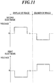
- a display device of the electrochromic system performs the display of an image and the erasion of the displayed image in the manner as shown in FIG. 11 , for example. That is, the display of image is performed by an energization to color the pixels which are selected (selection pixels), in which a negative voltage is applied to a line electrode (a first electrode) to form selection pixels, and a positive voltage is applied to a data electrode (a second electrode) to form the selection pixels. Further, the erasion of the displayed image is performed by an energization which is in the reverse direction of the energization performed to color the selection pixels, in which the positive voltage is applied to the first electrode, and the negative voltage is applied to the second electrode.
- an electrolyte solution is filled in between the electrodes.
- the electrodes to form the selection pixels are polarized, so as to bring about a state of such as an electrolyte capacitor, a battery cell, or the like. That is to say, after the energization to color the selection pixels is performed, an electric charge remains in between the electrodes which form the selection pixels. Such electric charge moves out to the surroundings through the electrolyte solution, to reach in between the electrodes which form the non-selection pixels. Accordingly, for example, when a high-speed scanning is performed to display a given image repeatedly, the next energization happens to be performed before the remaining electric charge has been eliminated.
- the electric charge is to be accumulated in between the electrodes which form the non-selection pixels, and the non-selection pixels happen to be colored.
- the selection pixels appear to be smudged.
- a partition wall be formed in between the pixels in order to prevent the remaining electric charge from moving so that the pixels are separated.
- forming such partition walls requires accuracy and meticulousness for positioning, and the like, thus results in a great deal of burden.
- the present invention is directed to realizing a high-speed display and a high-speed erasion of an image with high quality in an electrochromic display device which is driven by a passive matrix drive, without being provided with a partition wall.
- the display apparatus 1000 is the apparatus that is equipped with the electrochromic display device 100 and performs given display processing in accordance with image data input from the outside.
- the display apparatus 1000 includes the electrochromic display device 100, the first voltage switching sections 200, a first electrode selecting section 300, the second voltage switching sections 400, a second electrode selecting section 500, a control section 600, and the like.
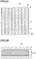
- the electrochromic display device 100 is the display device of a passive matrix drive that is composed of a first substrate 10, first electrodes 20 formed on the upper surface of the first substrate 10, a second substrate 30 provided above the first substrate 10 to be opposed to the first substrate 10, second electrodes 40 formed on the under surface of the second substrate 30, and an electrochromic composition layer 50 provided between the first substrate 10 and the second substrate 30.
- the electrochromic display device 100 is adapted to execute a display by energizations between the first electrodes 20 and the second electrodes 40, and to execute the erasion of the display by the energizations in the directions reverse to those of the energizations for the display between the first electrodes 20 and the second electrodes 40.
- the first electrodes 20 are, for example, a plurality of electrodes extending in parallel with each other.
- the second electrodes 40 are, for example, transparent display electrodes composed of a plurality of transparent electrodes extending in parallel with each other in the directions perpendicular to those of the first electrodes 20. Then, pixels 60 are formed in the regions in which the first electrodes 20 and the second electrodes 40 are in grade separated crossing.
- the first substrate 10 is formed in, for example, a plane, and has the function of the base substance of the electrochromic display device 100.
- the quality of material of the first substrate 10 is not especially limited as long as the material has an electrical insulation property.
- glass and plastic can be used as the first substrate 10.
- the glass for example, the following kinds of glass can be given: soda-lime glass, low-alkali borosilicate glass, no-alkali borosilicate glass, no-alkali aminosilicate glass, and silica glass.
- plastic for example, the following kinds of plastic can be given: polyesters, such as polyethylene terephthalate and polyethylene naphtahalate; polyamides; polycarbonates; fluorinated polymers, such as polyvinylidene fluoride; polyethers; polyolefins, such as polystyrene and polyethylene; and polyimides.
- the first substrate 10 looks white. Accordingly, when the quality of material of the first substrate 10 is glass or plastic, then it is possible to form the first substrate 10 that looks white by blending, for example, a white pigment, such as a titanium dioxide, a barium sulfate, and kaolin. Moreover, it is possible to form the first substrate 10 that looks white by applying the white pigment on the under surface of a transparent substrate, or by arranging a white sheet such as a sheet of white paper and a white polyethylene terephthalate (PET) sheet on the under surface.
- a white pigment such as a titanium dioxide, a barium sulfate, and kaolin.
- PET polyethylene terephthalate
- the first electrodes 20 are formed, for example, in lines, each having a width, and are provided in stripes in parallel with each other at regular intervals.
- the first electrodes 20 are provided on the upper surface of the first substrate 10 so as to contact with the electrochromic composition layer 50 and so as to be opposed to the second electrodes 40 with the electrochromic composition layer 50 put between the first and second electrodes 20 and 40.
- the first electrodes 20 have the functions of energizing the electrochromic composition layer 50 by being paired with the second electrodes 40.
- the first electrodes 20 form grade separated crossings with the second electrodes 40, that is, cross with the second electrodes 40 with intervals, and the pixels 60 are formed in the regions surrounded by the crossing points.
- the first electrodes 20 are not especially limited, and may be transparent electrodes or opaque electrodes as long as the electrodes are oxidized in at least their surfaces.
- the followings can be given: an indium tin oxide (ITO) thin film; a thin film including a coated oxide film of SnO 2 , InO 2 , or the like; an ITO thin film doped by Sn or Sb; a thin film including a coated oxide film of SnO 2 , InO 2 , or the like, and doped Sn or Sb; a zinc oxide thin film; a magnesium oxide thin film; an aluminum oxide thin film; a chromium oxide thin film; a nickel oxide thin film; and a titanium oxide thin film.
- the first electrodes 20 may be thin films each including a coated oxide film of an ITO, a zinc oxide, a magnesium oxide, an aluminum oxide, a chromium oxide, a nickel oxide, a titanium oxide, and the like.
- the second substrate 30 is, for example, a transparent substrate formed in a plane, and has the function as a supporting body of the second electrodes 40.
- the quality of material of the second substrate 30 is not especially limited as long as the material is the transparent substrate having an electrically insulation property.
- glass and plastic can be used as the second substrate 30.
- the glass for example, the following kinds of glass can be given: soda-lime glass, low-alkali borosilicate glass, no-alkali borosilicate glass, no-alkali aminosilicate glass, and silica glass.
- plastic for example, the following kinds of plastic can be given: polyesters, such as polyethylene terephthalate and polyethylene naphtahalate; polyamides; polycarbonates; fluorinated polymers, such as polyvinylidene fluoride; polyethers; polyolefins, such as polystyrene and polyethylene; and polyimides.
- the second electrodes 40 are, for example, transparent electrodes formed in lines, each having a width, and are provided in stripes parallel to each other at regular intervals.
- the second electrodes 40 are provided on the under surface of the second substrate 30 so as to contact with the electrochromic composition layer 50 and so as to be opposed to the first electrodes 20 with the electrochromic composition layer 50 put between the second electrode 40 and the first electrodes 20.
- the second electrodes 40 have the functions of energizing the electrochromic composition layer 50 by being paired with the first electrodes 20.
- the second electrodes 40 form grade separated crossings with the first electrodes 20, that is, cross with the first electrodes 20 with intervals, and the pixels 60 are formed in the regions surrounded by the crossing points.
- the second electrodes 40 are not especially limited as long as the second electrodes 40 may be the transparent electrodes oxidized in at least their surfaces.
- each of the second electrodes 40 for example, the followings can be given: an ITO thin film; a thin film including a coated oxide film of SnO 2 , InO 2 , or the like; an ITO thin film containing doped Sn or Sb; a thin film containing a coated oxide film of SnO 2 , InO 2 , or the like and doped Sn or Sb; a zinc oxide thin film; and a magnesium oxide thin film.
- the second electrodes 40 may be thin films, each including a coated oxide film or the like of an ITO, a zinc oxide, a magnesium oxide, an aluminum oxide, a chromium oxide, a nickel oxide, a titanium oxide, and the like.
- the electrochromic composition layer 50 comprises for example, a spacer 51, an electochromic composition 52 which is supported by the spacer 51, and the like.
- the thickness of the electrochromic composition layer 50 is not especially limited, but it is possible to effectively manifest the display functions of the electrochromic composition 52 by setting the thickness of the electrochromic composition layer 50 to be preferably within a range of 10-500 ⁇ m, or more preferably within a range of 30-200 ⁇ m.
- the spacer 51 has the roles of holding the electrochromic composition 52 of fixed volumes between the first substrate 10 and the second substrate 30. That is, the spacer 51 has the roles of supporting the electrochromic composition 52 between the first substrate 10 and the second substrate 30 by including the electrochromic composition 52, and the roles for controlling the quantities of the electrochromic composition 52 to be uniform by the thicknesses of the spacer 51.
- the spacer 51 may be formed of an arbitrary material as long as it fulfils the above described rolls.
- a plate-like body or a sheet-like body with porous property, a granular body (either with porous property or non-porous property), and the like, may be cited as the spacer 51.
- the electrochromic composition 52 may be introduced into fine pores of the spacer 51, thereby the electrochromic composition layer 50 may be formed.
- the electrochromic composition 52 may be introduced into the fine pores of the spacer 51 to form the electrochromic composition layer 50 after the spacer 51 is sandwiched by the first electrodes 20 (the first substrate 10 where the first electrodes 20 are provided) and the second electrodes 40 (the second substrate 30 where the second electrodes 40 are provided).
- the electrochromic composition layer 50 may be sandwiched by the first electrodes 20 and the second electrodes 40 after the electrochromic composition 52 is introduced into the fine pores of the spacer 51 to form the electrochromic composition layer 50.
- the plate-like body or the sheet-like body with porous property preferably has fine pores which penetrate the first substrate 10 and the second substrate 30 in the substantially perpendicular direction.
- an anodized alumina, a mesh (net)-like sheet material, and the like may be cited, although not limited to these.
- the spacer 51 and the electrochromic composition 52 which are mixed to be of a paste form may be sandwiched by the first electrodes 20 and the second electrodes 40, thereby the electrochromic composition layer 50 may be formed.
- the electrochromic composition 52 contains a supporting electrolyte, a polar solvent, and a leuco dye.
- display quality deterioration inhibitors compounds, each having a hydroquinone derivative and/or a catechol derivative, a ferrocene derivative, and a carbonyl group
- adsorbents 53 adsorbing the leuco dyes at the time of energizations for the erasions between the first electrodes 20 and the second electrodes 40 are added to the electrochromic composition 52.
- electrochromic composition 52 for example, a polymer compound for adjusting the physical properties (such as thickening) of electrochromic composition 52 can be given.
- the electrochromic composition 52 has the function of the coloring and the erasing of a display of the electrochromic display device 100.
- the electrochromic composition 52 performs the coloring by the energizations between the first electrodes 20 and the second electrodes 40, and performing the erasing by the energizations in the directions reverse to those of the energizations for the coloring or by intercepting the energizations for the coloring.
- the electrochromic composition 52 has only to have fluidity, and may be, for example, in the form of a liquid having low viscosity, in the form of paste having high viscosity, or in the form of a gel having small fluidity.
- the supporting electrolytes which are constituents of the electrochromic composition 52, have the functions of making currents easy to flow through the electrochromic composition 52.
- the supporting electrolytes contain compounds generally called molten salts.
- Each of the supporting electrolytes may use each compound individually, or may use a plurality of compounds in a mixed state.
- the supporting electrolytes so as to be 0.01-20 weight% of the whole weight of the electrochromic composition 52, and it is more preferable to add the supporting electrolytes so as to be 0.1-20 weight% of the whole weight in order to manifest the aforesaid function sufficiently.
- the supporting electrolytes are not especially limited as long as the supporting electrolytes are compounds having the aforesaid functions, and for example, the first supporting electrolyte compounds and/or the second supporting electrolyte compounds may be cited.
- the compounds of, NaClO 4 , LiClO 4 , KClO 4 , RbClO 4 , CsClO 4 , NH 4 ClO 4 , LiBF 4 , and LiPF 6 may be cited, although not limited to these.
- the second supporting electrolyte compounds for example, the compounds of, (CH 3 ) 4 NClO 4 , (C 2 H 5 ) 4 NClO 4 , (n-C 4 H 9 ) 4 NClO 4 , (CH 3 ) 4 NBF 4 , (C 2 H 5 ) 4 NBF 4 , (n-C 4 H 9 ) 4 NBF 4 , (CH 3 ) 4 NCl, (C 2 H 5 ) 4 NCl, (CH 3 ) 4 NBr, (C 2 H 5 ) 4 NBr, (n-C 4 H 9 ) 4 NBr, (n-C 4 H 9 ) 4 NI, C 6 H 5 (CH 3 ) 3 NClO 4 , C 6 H 5 (C 2 H 5 ) 3 NClO 4 , C 8 H 17 (CH 3 ) 3 NClO 4 , (C 2 H 5 ) 4 NPF 6 , (n-C 4 H 9 ) 4 NPF 6 , (CH 3 ) 4 NCF
- the polar solvent which is a constituent of the electrochromic composition 52, is at least a kind of organic solvents using supporting electrolytes and exhibiting energization properties, and has the function of accelerating the erasing of the colored leuco dye by intercepting a voltage and/or a current. Moreover, the polar solvent also fulfills the function of the solvent of a polymer compound when the polymer compound is added to the electrochromic composition 52.
- the polar solvent various polar solvents may be individually used, or two kinds or more of polar solvents may be used in suitable combinations with each other.
- the polar solvents for example, the followings can be given: N-methyl pyrrolidone, dimethylformamide, diethylformamide, N,N-dimethylacetamide, propylene carbonate, dimethyl sulfoxide, ⁇ -butyrolactone, acetonitrile, propionitrile, and butyronitrile.
- N,N-dimethylacetamide can be given as the especially preferable polar solvent.
- the leuco dye one of the constituents of the electrochromic composition 52, is a colorless or light-colored electron donative precursor of a dye, and is a compound to be colored by a developer, such as a phenolic compound, an acidic substance, or an electron-accepting substance.
- the leuco dye for example, the compounds which include lactone, lactam, sultone, spiropyran, ester, or an amide structure at their partial skeletons and can be practically colorless can be given.
- a triarylmethane compound, a bis-phenyl methane compound, a xanthenes compound, a fluoran compound, a thiazine compound, and a spiropyran compound can be given, but the leuco dye is not limited to the ones mentioned above.
- the leuco dye can perform the coloring of various colors by being suitably selected among the compounds mentioned above. Consequently, the display color of the electrochromic display device 100 using the leuco dyes can be suitably selected on the basis of the leuco dyes. To put it concretely, for example, in the case of using the leuco dyes coloring to be black, a black-and-white display and a gray display can be performed.
- the blending quantities of the leuco dyes depend on the solubility of the leuco dyes, it is difficult to unconditionally express the blending quantities, but it is necessary that sufficient quantities of the leuco dyes for coloring are blended.
- the display quality deterioration inhibitors to be added to the electrochromic composition 52 are compounds having the functions of suppressing the deteriorations of the display quality of the electrochromic display device 100 accompanying the repetition operations of the coloring and the erasing of the leuco dyes.
- the addition quantities of the display quality deterioration inhibitors are preferably 1-20 weight% of the contained quantities of the leuco dyes, and the addition quantities are more preferably 5-20 weight% in order to manifest the aforesaid functions sufficiently.
- Each of the display quality deterioration inhibitors is a mixture of a first display quality deterioration suppressing compound (hydroquinone derivative and/or catechol derivative), a second display quality deterioration suppressing compound (ferrocene derivative), and a third display quality deterioration suppressing compound (the compound containing a carbonyl group (acetophenone derivative and/or dibenzoyl derivative).
- Each of the adsorbents 53 to be added to the electrochromic composition 52 is, for example, an aluminum oxide and/or an aluminum hydroxide.
- the modes of the adsorbents 53 are not especially limited, but it is preferable to add the adsorbents 53 into the electrochromic composition 52 in the state of powder, to disperse the adsorbents 53 to be uniform by means of ultrasonic waves, a ball mill, or a homogenizer, such as a homomixer, and to use the adsorbents 53 as a dispersion liquid of the solution of the electrochromic composition 52.
- the addition quantity of each of the adsorbents 53 varies according to the activity ratios, the particle diameters, and the like of the aluminum oxide and/or the aluminum hydroxide to be used.
- any of an aluminum oxide having a small surface area, such as alpha alumina, a large aluminum oxide having a particle diameter of 10 ⁇ m or more, an aluminum hydroxide having a small surface area, and an aluminum hydroxide having a particle diameter of 10 ⁇ m or more has a small adsorption effect of the leuco dyes, and accordingly it is preferable to add 0.5-5 grams of each of them to 1 gram of the leuco dye in order to manifest a sufficient adsorption operation, and is more preferable to add 1-3 grams of each of them.
- any of an aluminum oxide having a large surface area such as gamma alumina, a small aluminum oxide having a particle diameter of 1 ⁇ m or less, an aluminum hydroxide having a large surface area, and an aluminum hydroxide having a small particle diameter of 1 ⁇ m or less has a large adsorption effect of the leuco dyes, and consequently the addition of 0.1-0.5 gram of each of them to 1 gram of the leuco dye manifests a sufficient adsorption operation.
- the class of activated alumina to be used for thin-layer chromatography or the like manifests a sufficient adsorption operation by adding 0.1-0.5 gram of the activated alumina to 1 gram of the leuco dye even when the activated alumina includes large particles each having a particle diameter of several tens ⁇ m.
- the adsorbents 53 adsorbing the leuco dyes can be easily obtained as commercially available products.
- the followings can be given: aluminum oxide 60G Neutral for thin-layer chromatography (having particle diameters of 4-50 ⁇ m) available from Merk & Co., Inc.; low soda alumina LS235 (particle diameter of 0.47 ⁇ m), activated alumina C200 (particle diameter of 4.4 ⁇ m), and aluminum hydroxide B1403 (particle diameter of 1.5 ⁇ m), all available from Nippon Light Metal Co., Ltd.; and gamma alumina KC501 (particle diameter of 1 ⁇ m) available from Sumitomo Chemical Co., Ltd.
- Each of the polymer compounds to be added to the electrochromic composition 52 has the function of heightening the viscosity of the electrochromic composition 52 to make the handling of them easily.
- Various polymer compounds may be used individually, or two kinds or more of the polymer compounds may be combined with each other to be used.
- the polymer compounds are used for heightening the viscosity of the electrochromic composition 52, and the properties of the electrochromic composition 52 in this case can be made to be in the forms of liquids having low viscosity, paste having high viscosity, and gels having small fluidity.
- the preferable blending quantities of the polymer compounds are 0.1-80 weight% of all the weights of the electrochromic composition 52.
- polyvinylidene fluoride a polyvinylidene chloride
- a polyalkylene oxide such as a polyethylene oxide
- polymethyl methacrylate polyacrylonitrile
- polycarbonate polycarbonate
- a polyvinyl formal such as polyvinyl butyral.
- polyvinyl butyral and polyvinylidene fluoride can be given.
- the electrochromic composition 52 described above is examples, and the other compositions introduced between the spacer 51 can be used as the electrochromic composition layer 50 as long as the compositions can be electrochemically colored.
- the display apparatus 1000 includes the plurality of first voltage switching sections 200 (for example, the same number as that of the first electrodes 20 included in the electrochromic display device 100), for example, as shown in FIG. 1 .
- Each of the first voltage switching sections 200 switches, for example, a voltage applied to the first electrode 20 connected to the first voltage switching section 200 between a positive voltage and a negative voltage.
- each of the first voltage switching sections 200 includes a first positive voltage power source 201 outputting a positive voltage, a first P channel transistor 202 functioning as a switch, a first negative voltage power source 203 outputting a negative voltage, a first N channel transistor 204 functioning as a switch, and the like.
- the first positive voltage power source 201 is adapted to be turned on and off by, for example, the first electrode selecting section 300. When the first positive voltage power source 201 is turned on, the positive voltage is applied to one end (source) of the first P channel transistor 202.
- the first P channel transistor 202 includes, for example, a gate connected to a gate terminal 200a, the one end (source) connected to the first positive voltage power source 201, and the other end (drain) connected to an output terminal 200b connected to the corresponding first electrode 20 of the electrochromic display device 100.
- the first negative voltage power source 203 is adapted to be turned on and off by, for example, the first electrode selecting section 300. When the first negative voltage power source 203 is turned on, the negative voltage is applied to one end (source) of the first N channel transistor 204.
- the first N channel transistor 204 includes, for example, a gate connected to the gate terminal 200a, the one end (source) connected to the first negative voltage power source 203, and the other end (drain) connected to the output terminal 200b connected to the corresponding first electrode 20 of the electrochromic display device 100.
- the first electrode selecting section 300 applies positive voltages and negative voltages to the first electrodes 20 (line electrodes) by controlling the first voltage switching sections 200 in conformity with, for example, control signals input from the control section 600.
- the first electrode selecting section 300 applies a predetermined positive voltage to the gate terminal 200a of one of the first voltage switching sections 200, and turns on the first positive voltage power source 201.
- the predetermined positive voltage is applied to the gate of the first P channel transistor 202, and the positive voltage from the first positive voltage power source 201 is applied to the one end (source) of the first P channel transistor 202. Consequently, the first P channel transistor 202 is turned on, and the positive voltage is applied to the corresponding first electrode 20 through the output terminal 200b.
- the first electrode selecting section 300 applies a predetermined negative voltage to the gate terminal 200a of the first voltage switching section 200, and turns on the first negative voltage power source 203.
- the predetermined negative voltage is applied to the gate of the first N channel transistor 204, and the negative voltage from the first negative voltage power source 203 is applied to the one end (source) of the first N channel transistor 204. Consequently, the first N channel transistor 204 is turned on, and the negative voltage is applied to the corresponding first electrode 20 through the output terminal 200b.
- the positive voltage applied to the first electrode 20 is referred to as “the second positive voltage”
- the negative voltage applied to the first electrode 20 is referred to as “the first negative voltage”.
- the display apparatus 1000 includes the plurality of second voltage switching sections 400 (for example, the same number as that of the second electrodes 40 included in the electrochromic display device 100).
- Each of the second voltage switching sections 400 switches, for example, a voltage applied to the second electrode 40 connected to the second voltage switching section 400 between a positive voltage and a negative voltage.
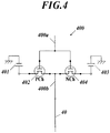
- each of the second voltage switching sections 400 includes a second positive voltage power source 401 outputting a positive voltage, a second P channel transistor 402 functioning as a switch, a second negative voltage power source 403 outputting a negative voltage, a second N channel transistor 404 functioning as a switch, and the like.
- the second positive voltage power source 401 is adapted to be turned on and off by, for example, the second electrode selecting section 500. When the second positive voltage power source 401 is turned on, the positive voltage is applied to one end (source) of the second P channel transistor 402.
- the second P channel transistor 402 includes, for example, a gate connected to a gate terminal 400a, the one end (source) connected to the second positive voltage power source 401, and the other end (drain) connected to an output terminal 400b connected to the corresponding second electrode 40 of the electrochromic display device 100.
- the second negative voltage power source 403 is adapted to be turned on and off by, for example, the second electrode selecting section 500. When the second negative voltage power source 403 is turned on, the negative voltage is applied to one end (source) of the second N channel transistor 404.
- the second N channel transistor 404 includes, for example, a gate connected to the gate terminal 400a, the one end (source) connected to the second negative voltage power source 403, and the other end (drain) connected to the output terminal 400b connected to the corresponding second electrode 40 of the electrochromic display device 100.
- the second electrode selecting section 500 applies positive voltages and negative voltages to the second electrodes 40 (data electrodes) by controlling the second voltage switching sections 400 in conformity with, for example, control signals input from the control section 600.
- the second electrode selecting section 500 applies a predetermined positive voltage to the gate terminal 400a of one of the second voltage switching sections 400, and turns on the second positive voltage power source 401.
- the predetermined positive voltage is applied to the gate of the second P channel transistor 402
- the positive voltage from the second positive voltage power source 401 is applied to the one end (source) of the second P channel transistor 402. Consequently, the second P channel transistor 402 is turned on, and the positive voltage is applied to the corresponding second electrode 40 through the output terminal 400b.
- the second electrode selecting section 500 applies a predetermined negative voltage to the gate terminal 400a of the second voltage switching section 400, and turns on the second negative voltage power source 403.
- the predetermined negative voltage is applied to the gate of the second N channel transistor 404, and the negative voltage from the second negative voltage power source 403 is applied to the one end (source) of the second N channel transistor 404. Consequently, the second N channel transistor 404 is turned on, and the negative voltage is applied to the corresponding second electrode 40 through the output terminal 400b.
- the positive voltage applied to the second electrode 40 is referred to as “the first positive voltage”
- the negative voltage applied to the second electrode 40 is referred to as “the second negative voltage”.
- the control section 600 includes, for example, a central processing unit (CPU), a read only memory (ROM), a random access memory (RAM), and the like, and controls the operation of each section constituting the display apparatus 1000 in a concentrated manner.
- CPU central processing unit
- ROM read only memory
- RAM random access memory
- the control section 600 controls the first electrode selecting section 300 and the second electrode selecting section 500 on the basis of image data input from, for example, the outside, to make the electrochromic display device 100 display the image based on the image data by a passive matrix drive through the first voltage switching sections 200 and the second voltage switching sections 400.
- the control section 600 selects a pixel to be colored, and applies the voltage of the first potential difference between the first electrode 20, used as a negative electrode, and the second electrode 40, used as a positive electrode, both constituting the selected pixel (selection pixel), to display the selection pixel.
- the control section 600 further applies the voltage of the second potential difference, which is equal to or more than the first potential difference between the first electrode 20, used as a positive electrode, and the second electrode 40, used as a negative electrode, both constituting the selected pixel (selection pixel), to color the selection pixel, and thereby the control section 600 makes the electrochromic display device 100 display an image.
- the first electrode selecting section 300 selects the first electrode 20 in an order of the line of the first row (for example, the first electrode 20 provided at the top in FIG. 1 ) ⁇ the second row ⁇ the third row ⁇ ... , according to the control signal input from the control section 600. For example, as shown in FIG. 5 , the first electrode selecting section 300 applies the first negative voltage to the selected first electrode 20, and immediately after that, the first electrode selecting section 300 applies the second positive voltage thereto.
- the plurality of first electrodes 20 are designed so as not to be selected together at the same time.
- the second electrode selecting section 500 selects the second electrode 40 in a state of being synchronized with the selection of the first electrode 20 by the first electrode selecting section 300, according to the control signal input from the control section 600. That is to say, when the first electrode 20 provided at the first row is selected by the first electrode selecting section 300, the second electrode selecting section 500 selects the second electrode 40 to form the pixel 60 to be colored provided at the first row. For example, as shown in FIG. 5 , the second electrode selecting section 500 applies the first positive voltage to the selected second electrode 40, and immediately after that, the second electrode selecting section 500 applies the second negative voltage thereto.
- the first negative voltage is applied to the first electrode 20, and the first positive voltage is applied to the second electrode 40, thereby the voltage of the first potential difference is applied between the electrodes.
- the second positive voltage is applied to the first electrode 20, and the second negative voltage is applied to the second electrode 40, thereby the voltage of the second potential difference is applied between the electrodes.
- the periods in which the voltage is not applied are indicated by virtual line (two-dot chain lines).
- the voltage in the first electrode 20 and in the second electrode 40 in the period in which the voltage is not applied is a voltage which remains naturally in the electrodes, which is actually not zero (0), thereby the periods are indicated by the virtual lines.
- the first potential difference can be set arbitrarily, as long as it is a voltage between the electrodes capable of coloring the pixels.
- the pixels colored by the applied voltage of the first potential difference are to be subjected to color degradation by the applied voltage of the second potential difference.
- the first potential difference may preferably be the voltage between the electrodes so that the color after the color degradation is to be the desirable color.
- the first potential difference depends on the material of the first electrode 20 and the second electrode 40, and the like, thus the concrete first potential difference is difficult to be generally expressed, however, it for example ranges in 5V ⁇ first potential difference ⁇ 8V.
- the second potential difference can be set arbitrarily, as long as it is a voltage between the electrodes capable of eliminating the electric charge generated in between the electrodes by the applied voltage of the first potential difference.
- the sum of the time of the applied voltage of the first potential difference (application period) and the time of the applied voltage of the second potential difference (application period) is determined according to the scanning speed (which is the vertical scanning frequency). Accordingly, the application time of the voltage of the first potential difference and the application time of the voltage of the second potential difference may be suitably changed arbitrarily according to the scanning speed.
- each of the current-voltage characteristics between the first and second electrodes 20 and 40 becomes nonlinear, for example, as shown in FIG. 6 . That is, each of the first electrodes 20 and the second electrodes 40 has the following characteristic: when a voltage larger than a first threshold value is applied between the electrodes 20 and 40 or a voltage smaller than a second threshold value is applied between the electrodes 20 and 40, a current flows between the electrodes 20 and 40; but when a voltage equal to or less than the first threshold value and equal to or larger than the second threshold value is applied between the electrodes 20 and 40, no currents flow between the electrodes 20 and 40.
- the first potential difference and the second potential difference are set to be the voltage making a current flow between the electrodes 20 and 40 constituting the selection pixels, and the voltage making no currents flow between the electrodes 20 and 40 constituting the non-selection pixels, then energizations are suppressed even when potential differences are generated between the electrodes 20 and 40 constituting the non-selection pixels around a selection pixel owing to an influence from the selection pixel. Consequently, the non-selection pixels are not colored, and only the selection pixel is colored. Thus, it is possible to display a high resolution image.
- the electrochromic display device 100 when the electrochromic display device 100 is driven at a high speed, then the nonlinearity of the current-voltage characteristics between the electrodes 20 and 40 is broken, and the non-selection pixels also become colored owing to leakage currents (by the remaining electric current being moved).
- the present invention performs energization (applied voltage of the first potential difference) to color the pixels in between the electrodes forming the selection pixels. Further, immediately after that, the energization (applied voltage of the second potential difference) in the reverse direction to eliminate the electric charge generated by the energization to color the pixels, thereby prevents generation of leakage currents.
- the control section 600 applies the first negative voltage (for example, -4.0V ⁇ first negative voltage ⁇ - 2.5V) to the line of the first row (the first electrode 20 in the first row), and applies the first positive voltage (for example, +2.5V ⁇ first positive voltage ⁇ +4.0V) to the second electrode 40 constituting a selection pixel among the pixels in the line of the first row. Thereby the control section 600 applies the voltage of the first potential difference between these electrodes 20 and 40.
- the control section 600 applies the second positive voltages (for example, +2.5V ⁇ second positive voltage ⁇ +6.0V) to the first electrodes 20, and applies the second negative voltages (for example, -6.0V ⁇ second negative voltage ⁇ -2.5V) to the second electrodes 40.
- the control section 600 applies the voltages of the second potential differences between the electrodes 20 and 40.
- a current flows from the second electrode 40 to the first electrode 20 through the electrochromic composition 52, and the electrochromic composition 52 causes an electrochemical change at the interface (on the surface of the second electrode 40) between the electrochromic composition layer 50 and the second electrode 40. Consequently, the selection pixel in the line of the first row is colored. Further, in between the electrodes constituting the pixels 60, the electric charge is generated as the voltage of the first potential difference is applied, however, the generated electric charge is to be eliminated by the application of the voltage of the second potential difference immediately after that.
- the control section 600 applies the first negative voltage to the line of the second row (the first electrode 20 in the second row), and applies the first positive voltage to the second electrode 40 constituting a selection pixel among the pixels in the line of the second row to apply the voltage of the first potential difference between these electrodes 20 and 40. Thereby, the control section 600 colors the selection pixel in the line of the second row.
- the control section 600 applies the second positive voltages to the first electrodes 20, and applies the second negative voltages to the second electrodes 40. Thereby the control section 600 applies the voltages of the second potential differences between these electrodes 20 and 40 so that the electric charge generated in between these electrodes as the voltage of the first potential difference is applied is to be eliminated.
- control section 600 performs the processing similar to that mentioned above to the third row, the fourth row, the fifth row, and so forth to make the electrochromic display device 100 display an image for 1 frame (1 page).
- control section 600 controls, for example, the first electrode selecting section 300 and the second electrode selecting section 500 to perform energizations in the directions reverse to those of the energizations for a display (coloring) through the first voltage switching sections 200 and the second voltage switching sections 400, that is, to make currents flow from the first electrodes 20 to the second electrodes 40. Thereby, the control section 600 erases the image displayed in the electrochromic display device 100.
- control section 600 erases the coloring of a selection pixel by applying a voltage of a third potential difference between the first electrode 20, used as a positive electrode, and the second electrode 40, used as a negative electrode, both constituting the selection pixel.
- the control section 600 thereby erases the image displayed in the electrochromic display device 100.
- the first electrode selecting section 300 selects the first electrode 20 in an order of the first row ⁇ the second row ⁇ the third row ⁇ .., according to the control signal input from the control section 600. For example, as shown in FIG. 5 , the first electrode selecting section 300 applies a predetermined positive voltage (hereinafter referred to as "a third positive voltage") to the selected first electrode 20.
- a third positive voltage a predetermined positive voltage
- the plurality of first electrodes 20 are designed so as not to be selected together at the same time.
- the second electrode selecting section 500 selects the second electrode 40 in a state of being synchronized with the selection of the first electrode 20 by the first electrode selecting section 300, according to the control signal input from the control section 600. That is to say, when the first electrode 20 provided at the first row is selected by the first electrode selecting section 300, the second electrode selecting section 500 selects the second electrode 40 to form the pixel 60 to be erased provided at the first row (which is the pixel 60 currently colored). For example, as shown in FIG. 5 , the second electrode selecting section 500 applies a predetermined negative voltage (hereinafter referred to as "a third negative voltage”) to the selected second electrode 40.
- a third negative voltage hereinafter referred to as "a third negative voltage
- the third positive voltage is applied to the first electrode 20, and the third negative voltage is applied to the second electrode 40, thereby the voltage of the third potential difference is applied between the electrodes.
- the third potential difference can be set arbitrarily, as long as it is a voltage between the electrodes capable of erasing the colored pixels 60.
- the third potential difference depends on the material of the first electrode 20 and the second electrode 40, and the like, thus the concrete third potential difference is difficult to be generally expressed, however, it for example ranges in 2.0V ⁇ third potential difference ⁇ 5.0V.
- the time of the applied voltage of the third potential difference is determined according to the scanning speed.
- the erasion of the image displayed in the electrochromic display device 100 is performed by the energizations in the directions reverse to those of the energizations for a display, or is performed by intercepting the energizations for the display and leaving the display apparatus 100 as it is, but the energizations in the directions reverse to those of the energizations for the display can execute the erasion operation more rapidly.
- the leuco dyes are adsorbed by the adsorbents 53 at the time of energizations for erasion, and consequently it can be prevented that the leuco dyes move to the interfaces (the surfaces of the first electrodes 20) between the electrochromic composition layer 50 and the first electrodes 20 and are colored.
- the leuco dyes are polarized in solutions.
- the adsorbents 53 have the features that their specific surface areas are large and their adsorption abilities are high, and their surfaces are polarized.
- the second electrodes 40 are positive electrodes in the energizations of a color display, the leuco dyes, which are electron donatives, give electrons to the second electrodes 40 to be colored. Thus a display is performed.
- the energizations are performed in the directions reverse to those of the energizations for the display in the energizations for erasion, the second electrodes 40 are used as the negative electrodes.
- the leuco dyes receive electrons from the second electrodes 40 of the negative electrodes to be erased, and thus the colors are erased. Then, the leuco dyes changed to be colorless move into the directions of the first electrodes 20, but the leuco dyes do not reach the first electrodes 20 owing to the existence of the adsorbents 53 having high adsorption abilities and polarized surfaces, and the leuco dyes move to the adsorbents 53 to be trapped and adsorbed.
- the electrochromic display device 100 of the present embodiment can prevent the leuco dyes from moving to the interfaces (the surfaces of the first electrodes 20) between the electrochromic composition layer 50 and the first electrodes 20 to be colored at the time of the energizations for erasion.
- a rectangular non-alkali glass substrate having a thickness of 0.7 mm was used as the second substrate 30, and an ITO was formed on one surface (the under surface) of the second substrate 30 by sputtering.
- the sputtered ITO had a film thickness of 200 nm and a surface resistance of 10 ⁇ / ⁇ .
- the ITO formed by the sputtering was patterned into stripes each having a width of 0.42 mm and a pitch of 0.45 mm by the use of the photolithographic method. Thus the second electrodes 40 were made.
- a rectangular non-alkali glass substrate was used as the first substrate 10, and chromium was formed on one surface (the upper surface) of the first substrate 10 by sputtering.
- An oxide film (chromium oxide) was formed on the surface of the sputtered chromium.
- the sputtered chromium (including the chromium oxide on the surface thereof) had a film thickness of 200 nm and a surface resistance of 1 ⁇ / ⁇ .
- the chromium (including the chromium oxide on the surface thereof) formed by the sputtering was patterned into stripes each having a width of 0.42 mm and a pitch of 0.45 mm by the use of the photolithographic method.
- the first electrodes 20 were made.
- the spacer 51 which is of granular body ("micro pearl” (particle diameter of 50 ⁇ m) available from Sekisui Chemical Co., Ltd.)
- the electrochromic composition 52 to which and predetermined additives (display quality deterioration inhibitors, adsorbents 53, polymer compounds, or the like) were added (hereinafter referred to as "electrochromic compositions A"), are mixed so as to be of a paste form are sandwiched by the first substrate 10 forming the first electrodes 20 and the second substrate 30 forming the second electrodes 40.
- the first electrodes 20 and the second electrodes 40 are adjusted so as to be perpendicular to each other and the pixels 60 are positioned at the intersecting portion, and thus the electrochromic display device 100 (hereinafter referred to as "display device A") was made.
- composition of each of the electrochromic compositions A was as follows:
- the first voltage switching sections 200 and the second voltage switching sections 400 were connected to the line electrodes (first electrodes 20) and data electrodes (second electrodes 40) of the display device A, respectively, and a display apparatus 1000 having the display device A was made as the electrochromic display device 100.
- the energizations for display were performed by the use of a passive matrix driving method.
- the first negative voltage (-3.5 V) was applied to the first electrode 20, and the first positive voltage (+3.5 V) was applied to the second electrode 40, thereby the voltage of the first potential difference (7.0 V) was applied in between the electrodes.
- the second positive voltage (+4.2 V) was applied to the first electrode 20 and the second negative voltage (-4.2 V) was applied to the second electrode 40, thereby the voltage of the second potential difference (8.4 V) was applied in between the electrodes.
- this voltage application processing was performed for each line in a predetermined speed, so as to perform scanning, thereby an image was displayed. Further, the scanning was performed repeatedly, thereby the image was displayed repeatedly.
- example 1-1 was performed with the scanning under the speed of 8 msec/ 1 line, and example 1-2 was performed therewith under the speed of 2 msec/ 1 line.
- an image was displayed by applying voltage performed for the conventional electrochromic display device (that is to say, the energization in the reverse direction is not performed immediately after the energization to color the pixels (see FIG. 11 )).
- a display apparatus 1000 including the display device A was used, wherein a predetermined negative voltage (-2.0 V) was applied to the first electrode 20, and a predetermined positive voltage (+2.0 V) was applied to the second electrode 40, thereby the voltage of a predetermined potential difference (4.0 V) was applied in between the electrodes.
- this voltage application processing was performed for each line in a predetermined speed, so as to perform scanning, thereby an image was displayed. Further, the scanning was performed repeatedly, thereby the image was displayed repeatedly.
- comparative example 1-1 was performed with the scanning under the speed of 8 msec/ 1 line, and comparative example 1-2 was performed therewith under the speed of 2 msec/ 1 line.
- FIG. 7 shows a part of an image displayed in the example 1-1
- FIG. 8 shows a part of an image displayed in the example 1-2
- FIG. 9 shows a part of an image displayed in the comparative example 1-1
- FIG. 10 shows a part of an image displayed in the comparative example 1-2.
- the electrochromic display device 100 comprising: a first substrate 10; a first electrode 20 provided in an upper surface of the first substrate 10; a second substrate 30 formed by a transparent material, the second substrate 30 being provided above the first substrate 10 to be opposed to the first substrate 10; a second electrode 40 provided in a lower surface of the second substrate 30, at least a part of the second electrode 40 being formed by a transparent electrode material; and an electrochromic composition layer 50 provided in between the first substrate 10 and the second substrate 30, wherein the electrochromic display device 100 is driven by a passive matrix drive in which the electrochromic display device 100 performs a display by an energization between the first electrode 20 and the second electrode 40, and performs an erasion of the display by an energization in a direction reverse to a direction of the energization between the first electrode 20 and the second electrode 40 for the display, wherein the first electrode 20 comprises a plurality of electrodes which extend parallely, wherein the second electrode 40
- the energization in the reverse direction (with reverse polarity) from that of the energization to color the selection pixels is performed so as to eliminate the electric charge generated in between the electrodes constituting the selection pixels, thereby the electric charge is prevented from remaining. Accordingly, the non-selection pixels are not colored without the influence from the remaining electric charge, and the erasion of the displayed image does not take much time without the same. Thus, the high-speed display of an image with high quality can be realized, without being provided with a partition wall.
- the electrochromic display device 100 wherein a ratio of an application time of the voltage of the second potential difference to an application time of the voltage of the first potential difference ranges in 0.25 to 0.5.
- the electric charge generated in between the electrodes forming the selection pixels can reliably be eliminated.
- the first application processing is performed. That is, the voltage of the first potential difference is applied in between the electrodes in a state where the first electrode 20 constituting the selection pixel is the negative electrode, and the second electrode 40 constituting the selection pixel is the positive electrode. Further, immediately after that, the voltage of the second potential difference which is equal to or more than the first potential difference is applied in between the electrodes, in a state where the first electrode 20 constituting the selection pixel is the positive electrode, and the second electrode 40 constituting the selection pixel is the negative electrode.
- the leuco dyes are moved in between the electrochromic composition layer 50 and the second electrode 40 (the surface of the second electrode 40) so as to be colored, thereby the image displayed from the upper surface side of the second substrate 30 is observed.
- the present invention is not limited to this.
- the followings can also be performed.
- the second application processing is performed. That is, the voltage of the first potential difference is applied in between the electrodes in a state where the first electrode 20 constituting the selection pixel is the positive electrode, and the second electrode 40 constituting the selection pixel is the negative electrode.
- the voltage of the second potential difference which is equal to or more than the first potential difference is applied in between the electrodes, in a state where the first electrode 20 constituting the selection pixel is the negative electrode, and the second electrode 40 constituting the selection pixel is the positive electrode. Still further, the leuco dyes are moved in between the electrochromic composition layer 50 and the first electrode 20 (the surface of the first electrode 20) so as to be colored.
- the image displayed from the upper surface side of the second substrate 30 can be observed, through the second substrate 30, the second electrodes 40 and the electrochromic composition layer 50.
- the first application processing and the second application processing may be performed one after the other.
- each of the first voltage switching sections 200 and each of the second voltage switching sections 400 are not limited to those shown in FIGS. 3 and 4 , respectively, but the circuit configurations of the first and second voltage switching sections 200 and 400 may be set arbitrarily as long as the following can be performed. That is, at the time of the display operation, the voltage of the first potential difference is applied in between the electrodes in a state where the first electrode 20 constituting the selection pixel is the negative electrode, and the second electrode 40 constituting the selection pixel is the positive electrode.
- the voltage of the second potential difference which is equal to or more than the first potential difference is applied in between the electrodes, in a state where the first electrode 20 constituting the selection pixel is the positive electrode, and the second electrode 40 constituting the selection pixel is the negative electrode.
- the voltage was not applied in between the electrodes other than the ones constituting the selection pixels, however, the present invention is not limited to the above described. It is also possible to apply a predetermined low voltage or to supply a predetermined low current to the electrodes other than the ones constituting the selection pixels, so that the energization in the reverse direction from that between the electrodes constituting the selection pixels may be performed in between the electrodes other than the ones constituting the selection pixels. Thereby, the generation of the leakage current can further be suppressed.
Landscapes
- Engineering & Computer Science (AREA)
- Physics & Mathematics (AREA)
- Computer Hardware Design (AREA)
- General Physics & Mathematics (AREA)
- Theoretical Computer Science (AREA)
- Electrochromic Elements, Electrophoresis, Or Variable Reflection Or Absorption Elements (AREA)
- Devices For Indicating Variable Information By Combining Individual Elements (AREA)
- Control Of Indicators Other Than Cathode Ray Tubes (AREA)
Claims (3)
- Eine elektrochrome Anzeigevorrichtung (100) aufweisend:ein erstes Substrat (10),eine erste Elektrode (20) bereitgestellt in einer oberen Fläche des ersten Substrats (10),ein zweites Substrat (30), das durch ein transparentes Material geformt ist, das zweite Substrat (30) ist oberhalb des ersten Substrats (10) bereitgestellt, um gegenüberliegend zu dem ersten Substrat (10) zu sein,eine zweite Elektrode (40) bereitgestellt in einer unteren Fläche des zweiten Substrats (30), zumindest ein Teil der zweiten Elektrode (40) ist durch ein transparentes Elektrodenmaterial geformt, und eine elektrochrome Zusammensetzungsschicht (40) ist zwischen dem ersten Substrat (10) und dem zweiten Substrat (30) vorgesehen, wobei die elektrochrome Anzeigevorrichtung (100) konfiguriert ist, um durch einen passiven Matrixantrieb angetrieben zu werden, bei dem die elektrochrome Anzeigevorrichtung (100) konfiguriert ist, um eine Anzeige durch Energetisierung zwischen der ersten Elektrode (20) und der zweiten Elektrode (40) durchzuführen, und konfiguriert ist, um ein Löschen der Anzeige durch Energetisierung in einer Richtung entgegengesetzt zu einer Richtung der Energetisierung zwischen der ersten Elektrode (20) und der zweiten Elektrode (40) zum Anzeigen durchzuführen, wobeidie erste Elektrode (20) eine Vielzahl von Elektroden aufweist, die sich parallel erstrecken, wobei die zweite Elektrode (40) eine Vielzahl von transparenten Anzeigeelektroden enthält, die sich parallel in einer Richtung rechtwinklig zu einer Erstreckungsrichtung der ersten Elektrode (20) erstrecken, wobeiein Pixel (60) in jeder Region geformt ist, wo die erste Elektrode (20) und die zweite Elektrode (40) sich einander geneigt getrennt kreuzen, d.h. wo die erste Elektrode (20) sich mit der zweiten Elektrode (40) mit einem Abstand kreuzt,dadurch gekennzeichnet, dass die elektrochrome Anzeigevorrichtung (100) so konfiguriert ist, dass, wenn die Anzeige durchgeführt wird, eine erste Anwendungsspannungsverarbeitung für jedes ausgewählte Pixel durchgeführt wird, welches ein Pixel zum Farbgeben ist, bei dem: (i) die erste Elektrode (20), die das ausgewählte Pixel (60) formt, als eine negative Elektrode gesetzt ist, und die zweite Elektrode (40), die zweite ausgewählte Pixel (60) formt, als eine positive Elektrode gesetzt ist, um eine Spannung einer ersten Potentialdifferenz zwischen der ersten Elektrode (20) und der zweiten Elektrode (40) anzulegen, unmittelbar darauffolgend durch (ii) die erste Elektrode (20), die als die positive Elektrode gesetzt ist, und die zweite Elektrode (40) ist als die negative Elektrode gesetzt ist, um eine Spannung einer zweiten Potentialdifferenz anzuwenden, die gleich ist oder mehr ist als die erste Potentialdifferenz zwischen der ersten Elektrode (20) und der zweiten Elektrode (40),wobei die elektrochrome Anzeigevorrichtung so konfiguriert ist, dass ein Verhältnis der Spannung von der ersten Potentialdifferenz zu der Spannung der zweiten Potentialdifferenz von 1:1 zu 1:1,5 reicht, und ein Verhältnis einer Anwendungszeit der Spannung der ersten Potentialdifferenz zu einer Anwendungszeit der Spannung der zweiten Potentialdifferenz von 1:0,25 bis 1:0,5 reicht, so dass die Anzeige auch noch durchgeführt wird, selbst nachdem die Spannung der zweiten Potentialdifferenz angewendet worden ist.
- Eine elektrochrome Anzeigevorrichtung (100) aufweisend:ein erstes Substrat (10),eine erste Elektrode (20) bereitgestellt in einer oberen Fläche des ersten Substrats (10),ein zweites Substrat (30), das durch ein transparentes Material geformt ist, das zweite Substrat (30) ist oberhalb des ersten Substrats (10) bereitgestellt, um gegenüberliegend zu dem ersten Substrat (10) zu sein,eine zweite Elektrode (40) bereitgestellt in einer unteren Fläche des zweiten Substrats (30), zumindest ein Teil der zweiten Elektrode (40) ist durch ein transparentes Elektrodenmaterial geformt, und eine elektrochrome Zusammensetzungsschicht (40) ist zwischen dem ersten Substrat (10) und dem zweiten Substrat (30) vorgesehen, wobei die elektrochrome Anzeigevorrichtung (100) konfiguriert ist, um durch einen passiven Matrixantrieb angetrieben zu werden, bei dem die elektrochrome Anzeigevorrichtung (100) konfiguriert ist, um eine Anzeige durch Energetisierung zwischen der ersten Elektrode (20) und der zweiten Elektrode (40) durchzuführen, und konfiguriert ist, um ein Löschen der Anzeige durch Energetisierung in einer Richtung entgegengesetzt zu einer Richtung der Energetisierung zwischen der ersten Elektrode (20) und der zweiten Elektrode (40) zum Anzeigen durchzuführen, wobeidie erste Elektrode (20) eine Vielzahl von Elektroden aufweist, die sich parallel erstrecken,wobei die zweite Elektrode (40) eine Vielzahl von transparenten Anzeigeelektroden enthält, die sich parallel in einer Richtung rechtwinklig zu einer Erstreckungsrichtung der ersten Elektrode (20) erstrecken, wobeiein Pixel (60) in jeder Region geformt ist, wo die erste Elektrode (20) und die zweite Elektrode (40) sich einander geneigt getrennt kreuzen, d.h. wo die erste Elektrode (20) sich mit der zweiten Elektrode (40) mit einem Abstand kreuzt,dadurch gekennzeichnet, dass die elektrochrome Anzeigevorrichtung (100) so konfiguriert ist, dass, wenn die Anzeige durchgeführt wird, eine Anwendungsspannungsverarbeitung für jedes ausgewählte Pixel durchgeführt wird, welches ein Pixel zum Farbgeben ist, bei dem: (i) die erste Elektrode (20) die das ausgewählte Pixel (60) formt, als eine positive Elektrode gesetzt ist, und die zweite Elektrode (40), die das ausgewählte Pixel (60) formt, als eine negative Elektrode gesetzt ist, um eine Spannung einer ersten Potentialdifferenz zwischen der ersten Elektrode (20) und der zweiten Elektrode (40) anzuwenden, unmittelbar gefolgt durch (ii) die erste Elektrode (20), die als negative Elektrode gesetzt ist, und die zweite Elektrode (40), die als die zweite positive Elektrode gesetzt ist, um eine Spannung einer zweiten Potentialdifferenz anzulegen, die gleich oder mehr ist als die erste Potentialdifferenz zwischen der ersten Elektrode (20) und der zweiten Elektrode (40),wobei die elektrochrome Anzeigevorrichtung (100) so konfiguriert ist, dass ein Verhältnis der Spannung der ersten Potentialdifferenz zu der Spannung der zweiten Potentialdifferenz von 1:1 zu 1:1,5 reicht, und ein Verhältnis einer Anwendungszeit der Spannung der ersten Potentialdifferenz zu einer Anwendungszeit der Spannung der zweiten Potentialdifferenz von 1:0,25 bis 1:0,5 reicht, so dass die Anzeige auch noch durchgeführt wird, selbst nachdem die Spannung der zweiten Potentialdifferenz angewendet worden ist.
- Eine elektrochrome Anzeigevorrichtung (100) wie in Anspruch 1 beansprucht, wobei die elektrochrome Anzeigevorrichtung (100) so konfiguriert ist, dass, wenn die Anzeige durchgeführt wird, die erste Anwendungsspannungsverarbeitung und eine zweite Anwendungsspannungsverarbeitung nacheinander durchgeführt werden, wobei die zweite Anwendungsspannungsverarbeitung beinhaltet: (iii) die erste Elektrode (20) die das ausgewählte Pixel (60) formt, als eine positive Elektrode gesetzt ist, und die zweite Elektrode (40), die das ausgewählte Pixel (60) formt, als eine negative Elektrode gesetzt ist, zum Anwenden einer Spannung einer ersten Potentialdifferenz zwischen der ersten Elektrode (20) und der zweiten Elektrode (40), unmittelbar gefolgt von (iv) der ersten Elektrode (20), die als die negative Elektrode gesetzt ist, und die zweite Elektrode (40), die als die positive Elektrode gesetzt ist, um eine Spannung einer zweiten Potentialdifferenz anzuwenden, die gleich ist oder mehr ist als die erste Potentialdifferenz zwischen der ersten Elektrode (20) und der zweiten Elektrode (40),
wobei die elektrochrome Anzeigevorrichtung (100) so konfiguriert ist, dass während der zweiten Anwendungsspannungsverarbeitung ein Verhältnis der Spannung der ersten Potentialdifferenz zu der Spannung der zweiten Potentialdifferenz zwischen 1:1 bis 1:1,5 reicht, und ein Verhältnis einer Anwendungszeit der Spannung der ersten Potentialdifferenz zu einer Anwendungszeit der Spannung der zweiten Potentialdifferenz von 1:0,25 bis 1:0,5 reicht, so dass die Anzeige auch noch durchgeführt wird, selbst nachdem die Spannung der zweiten Potentialdifferenz angewendet worden ist.
Applications Claiming Priority (1)
| Application Number | Priority Date | Filing Date | Title |
|---|---|---|---|
| JP2009110286A JP5620070B2 (ja) | 2009-04-30 | 2009-04-30 | エレクトロクロミック表示デバイス |
Publications (2)
| Publication Number | Publication Date |
|---|---|
| EP2246842A1 EP2246842A1 (de) | 2010-11-03 |
| EP2246842B1 true EP2246842B1 (de) | 2017-04-05 |
Family
ID=42470711
Family Applications (1)
| Application Number | Title | Priority Date | Filing Date |
|---|---|---|---|
| EP10161643.1A Not-in-force EP2246842B1 (de) | 2009-04-30 | 2010-04-30 | Elektrochrome Anzeigevorrichtung |
Country Status (3)
| Country | Link |
|---|---|
| US (1) | US8526095B2 (de) |
| EP (1) | EP2246842B1 (de) |
| JP (1) | JP5620070B2 (de) |
Families Citing this family (7)
| Publication number | Priority date | Publication date | Assignee | Title |
|---|---|---|---|---|
| JP2557503Y2 (ja) | 1991-11-08 | 1997-12-10 | セイレイ工業株式会社 | 洗浄装置 |
| JP5879752B2 (ja) * | 2011-06-02 | 2016-03-08 | 船井電機株式会社 | 表示装置 |
| JP5891755B2 (ja) * | 2011-12-02 | 2016-03-23 | 船井電機株式会社 | 表示装置 |
| US20140023195A1 (en) * | 2012-07-23 | 2014-01-23 | Electronics And Telecommunications Research Institute | Radio frequency identification (rfid) tag, interrogator, and method for authentication between the rfid tag and the interrogator |
| JP6189151B2 (ja) * | 2013-09-13 | 2017-08-30 | 株式会社ジャパンディスプレイ | 表示装置 |
| US11227522B2 (en) * | 2017-10-24 | 2022-01-18 | Ppg Industries Ohio, Inc. | Pulsed electrochromic control for a panel and method of use |
| CN115327830A (zh) * | 2022-08-15 | 2022-11-11 | 海信视像科技股份有限公司 | 一种显示装置及其驱动方法 |
Family Cites Families (10)
| Publication number | Priority date | Publication date | Assignee | Title |
|---|---|---|---|---|
| JPS5273052A (en) * | 1975-12-15 | 1977-06-18 | Seiko Epson Corp | Device for operating electrochromics indicator |
| JPH01105917A (ja) * | 1987-10-19 | 1989-04-24 | Brother Ind Ltd | エレクトロクロミック表示装置 |
| JPH02135321A (ja) * | 1988-11-16 | 1990-05-24 | Sanyo Chem Ind Ltd | エレクトロクロミック素子 |
| DE60226581D1 (de) | 2001-03-30 | 2008-06-26 | Sony Corp | Anzeigeeinheit und ansteuerverfahren dafür |
| JP2003270671A (ja) | 2002-03-15 | 2003-09-25 | Fuji Photo Film Co Ltd | エレクトロクロミック装置 |
| WO2004001496A1 (en) | 2002-06-24 | 2003-12-31 | Koninklijke Philips Electronics N.V. | Electrochromic display panel with electrodes for adjusting crosstalk |
| SE0300541D0 (sv) * | 2003-02-28 | 2003-02-28 | Maarten Edwards | Method of controlling an electrohromic matrix display and electrochromic matrix display |
| JP5053585B2 (ja) | 2006-07-27 | 2012-10-17 | 株式会社船井電機新応用技術研究所 | エレクトロクロミック表示素子 |
| KR101377770B1 (ko) * | 2007-06-20 | 2014-03-26 | 삼성전자주식회사 | 전기변색 소자용 전극의 제조방법 |
| JP2009110286A (ja) | 2007-10-30 | 2009-05-21 | Toshiba Corp | 情報処理装置、ランチャー起動制御プログラムおよびランチャー起動制御方法 |
-
2009
- 2009-04-30 JP JP2009110286A patent/JP5620070B2/ja not_active Expired - Fee Related
-
2010
- 2010-04-29 US US12/770,022 patent/US8526095B2/en not_active Expired - Fee Related
- 2010-04-30 EP EP10161643.1A patent/EP2246842B1/de not_active Not-in-force
Non-Patent Citations (1)
| Title |
|---|
| None * |
Also Published As
| Publication number | Publication date |
|---|---|
| JP2010261983A (ja) | 2010-11-18 |
| JP5620070B2 (ja) | 2014-11-05 |
| US8526095B2 (en) | 2013-09-03 |
| EP2246842A1 (de) | 2010-11-03 |
| US20100277787A1 (en) | 2010-11-04 |
Similar Documents
| Publication | Publication Date | Title |
|---|---|---|
| US7995262B2 (en) | Electrochromic display device | |
| EP2246842B1 (de) | Elektrochrome Anzeigevorrichtung | |
| KR102788621B1 (ko) | 고속의 고-콘트라스트 광학 상태 스위칭을 제공하는 4 입자 전기영동 매체 | |
| US8976162B2 (en) | Electrophoretic display device, driving method of the same, and electronic apparatus | |
| JPWO2002079868A1 (ja) | 表示装置及びその駆動方法 | |
| KR101754799B1 (ko) | 화소 회로, 이를 포함하는 디스플레이 장치 및 디스플레이 장치의 구동방법 | |
| TW201521005A (zh) | 電致變色顯示裝置及驅動方法 | |
| US8467119B2 (en) | Electrochromic display device | |
| JP5879752B2 (ja) | 表示装置 | |
| JP5891755B2 (ja) | 表示装置 | |
| US12406631B2 (en) | Multi-particle electrophoretic display having low-flash image updates | |
| KR20220083765A (ko) | 전기 광학 디스플레이들을 구동하기 위한 방법들 | |
| US12394388B2 (en) | Time-shifted waveforms for multi-particle electrophoretic displays providing low-flash image updates | |
| HK40126618A (zh) | 用於多粒子电泳显示器的提供低闪光图像更新的时移波形 | |
| KR20020081423A (ko) | 리셋을 갖는 광 스위칭 장치 | |
| JPS614030A (ja) | エレクトロクロミツク表示装置 |
Legal Events
| Date | Code | Title | Description |
|---|---|---|---|
| PUAI | Public reference made under article 153(3) epc to a published international application that has entered the european phase |
Free format text: ORIGINAL CODE: 0009012 |
|
| AK | Designated contracting states |
Kind code of ref document: A1 Designated state(s): AT BE BG CH CY CZ DE DK EE ES FI FR GB GR HR HU IE IS IT LI LT LU LV MC MK MT NL NO PL PT RO SE SI SK SM TR |
|
| AX | Request for extension of the european patent |
Extension state: AL BA ME RS |
|
| 17P | Request for examination filed |
Effective date: 20110502 |
|
| 17Q | First examination report despatched |
Effective date: 20111202 |
|
| RAP1 | Party data changed (applicant data changed or rights of an application transferred) |
Owner name: FUNAI ELECTRIC CO., LTD. Owner name: TOKAI UNIVERSITY EDUCATIONAL SYSTEM |
|
| GRAP | Despatch of communication of intention to grant a patent |
Free format text: ORIGINAL CODE: EPIDOSNIGR1 |
|
| INTG | Intention to grant announced |
Effective date: 20161014 |
|
| GRAS | Grant fee paid |
Free format text: ORIGINAL CODE: EPIDOSNIGR3 |
|
| GRAA | (expected) grant |
Free format text: ORIGINAL CODE: 0009210 |
|
| AK | Designated contracting states |
Kind code of ref document: B1 Designated state(s): AT BE BG CH CY CZ DE DK EE ES FI FR GB GR HR HU IE IS IT LI LT LU LV MC MK MT NL NO PL PT RO SE SI SK SM TR |
|
| REG | Reference to a national code |
Ref country code: GB Ref legal event code: FG4D |
|
| REG | Reference to a national code |
Ref country code: CH Ref legal event code: EP |
|
| REG | Reference to a national code |
Ref country code: AT Ref legal event code: REF Ref document number: 882466 Country of ref document: AT Kind code of ref document: T Effective date: 20170415 |
|
| REG | Reference to a national code |
Ref country code: IE Ref legal event code: FG4D |
|
| REG | Reference to a national code |
Ref country code: DE Ref legal event code: R096 Ref document number: 602010041239 Country of ref document: DE |
|
| REG | Reference to a national code |
Ref country code: NL Ref legal event code: MP Effective date: 20170405 |
|
| REG | Reference to a national code |
Ref country code: LT Ref legal event code: MG4D |
|
| REG | Reference to a national code |
Ref country code: AT Ref legal event code: MK05 Ref document number: 882466 Country of ref document: AT Kind code of ref document: T Effective date: 20170405 |
|
| PG25 | Lapsed in a contracting state [announced via postgrant information from national office to epo] |
Ref country code: NL Free format text: LAPSE BECAUSE OF FAILURE TO SUBMIT A TRANSLATION OF THE DESCRIPTION OR TO PAY THE FEE WITHIN THE PRESCRIBED TIME-LIMIT Effective date: 20170405 |
|
| PG25 | Lapsed in a contracting state [announced via postgrant information from national office to epo] |
Ref country code: HR Free format text: LAPSE BECAUSE OF FAILURE TO SUBMIT A TRANSLATION OF THE DESCRIPTION OR TO PAY THE FEE WITHIN THE PRESCRIBED TIME-LIMIT Effective date: 20170405 Ref country code: NO Free format text: LAPSE BECAUSE OF FAILURE TO SUBMIT A TRANSLATION OF THE DESCRIPTION OR TO PAY THE FEE WITHIN THE PRESCRIBED TIME-LIMIT Effective date: 20170705 Ref country code: FI Free format text: LAPSE BECAUSE OF FAILURE TO SUBMIT A TRANSLATION OF THE DESCRIPTION OR TO PAY THE FEE WITHIN THE PRESCRIBED TIME-LIMIT Effective date: 20170405 Ref country code: LT Free format text: LAPSE BECAUSE OF FAILURE TO SUBMIT A TRANSLATION OF THE DESCRIPTION OR TO PAY THE FEE WITHIN THE PRESCRIBED TIME-LIMIT Effective date: 20170405 Ref country code: ES Free format text: LAPSE BECAUSE OF FAILURE TO SUBMIT A TRANSLATION OF THE DESCRIPTION OR TO PAY THE FEE WITHIN THE PRESCRIBED TIME-LIMIT Effective date: 20170405 Ref country code: GR Free format text: LAPSE BECAUSE OF FAILURE TO SUBMIT A TRANSLATION OF THE DESCRIPTION OR TO PAY THE FEE WITHIN THE PRESCRIBED TIME-LIMIT Effective date: 20170706 Ref country code: AT Free format text: LAPSE BECAUSE OF FAILURE TO SUBMIT A TRANSLATION OF THE DESCRIPTION OR TO PAY THE FEE WITHIN THE PRESCRIBED TIME-LIMIT Effective date: 20170405 |
|
| PG25 | Lapsed in a contracting state [announced via postgrant information from national office to epo] |
Ref country code: IS Free format text: LAPSE BECAUSE OF FAILURE TO SUBMIT A TRANSLATION OF THE DESCRIPTION OR TO PAY THE FEE WITHIN THE PRESCRIBED TIME-LIMIT Effective date: 20170805 Ref country code: BG Free format text: LAPSE BECAUSE OF FAILURE TO SUBMIT A TRANSLATION OF THE DESCRIPTION OR TO PAY THE FEE WITHIN THE PRESCRIBED TIME-LIMIT Effective date: 20170705 Ref country code: LV Free format text: LAPSE BECAUSE OF FAILURE TO SUBMIT A TRANSLATION OF THE DESCRIPTION OR TO PAY THE FEE WITHIN THE PRESCRIBED TIME-LIMIT Effective date: 20170405 Ref country code: PL Free format text: LAPSE BECAUSE OF FAILURE TO SUBMIT A TRANSLATION OF THE DESCRIPTION OR TO PAY THE FEE WITHIN THE PRESCRIBED TIME-LIMIT Effective date: 20170405 Ref country code: SE Free format text: LAPSE BECAUSE OF FAILURE TO SUBMIT A TRANSLATION OF THE DESCRIPTION OR TO PAY THE FEE WITHIN THE PRESCRIBED TIME-LIMIT Effective date: 20170405 |
|
| REG | Reference to a national code |
Ref country code: CH Ref legal event code: PL |
|
| REG | Reference to a national code |
Ref country code: DE Ref legal event code: R097 Ref document number: 602010041239 Country of ref document: DE |
|
| REG | Reference to a national code |
Ref country code: IE Ref legal event code: MM4A |
|
| PG25 | Lapsed in a contracting state [announced via postgrant information from national office to epo] |
Ref country code: DK Free format text: LAPSE BECAUSE OF FAILURE TO SUBMIT A TRANSLATION OF THE DESCRIPTION OR TO PAY THE FEE WITHIN THE PRESCRIBED TIME-LIMIT Effective date: 20170405 Ref country code: CZ Free format text: LAPSE BECAUSE OF FAILURE TO SUBMIT A TRANSLATION OF THE DESCRIPTION OR TO PAY THE FEE WITHIN THE PRESCRIBED TIME-LIMIT Effective date: 20170405 Ref country code: RO Free format text: LAPSE BECAUSE OF FAILURE TO SUBMIT A TRANSLATION OF THE DESCRIPTION OR TO PAY THE FEE WITHIN THE PRESCRIBED TIME-LIMIT Effective date: 20170405 Ref country code: SK Free format text: LAPSE BECAUSE OF FAILURE TO SUBMIT A TRANSLATION OF THE DESCRIPTION OR TO PAY THE FEE WITHIN THE PRESCRIBED TIME-LIMIT Effective date: 20170405 Ref country code: MC Free format text: LAPSE BECAUSE OF FAILURE TO SUBMIT A TRANSLATION OF THE DESCRIPTION OR TO PAY THE FEE WITHIN THE PRESCRIBED TIME-LIMIT Effective date: 20170405 Ref country code: EE Free format text: LAPSE BECAUSE OF FAILURE TO SUBMIT A TRANSLATION OF THE DESCRIPTION OR TO PAY THE FEE WITHIN THE PRESCRIBED TIME-LIMIT Effective date: 20170405 |
|
| PLBE | No opposition filed within time limit |
Free format text: ORIGINAL CODE: 0009261 |
|
| STAA | Information on the status of an ep patent application or granted ep patent |
Free format text: STATUS: NO OPPOSITION FILED WITHIN TIME LIMIT |
|
| PG25 | Lapsed in a contracting state [announced via postgrant information from national office to epo] |
Ref country code: LU Free format text: LAPSE BECAUSE OF NON-PAYMENT OF DUE FEES Effective date: 20170430 Ref country code: LI Free format text: LAPSE BECAUSE OF NON-PAYMENT OF DUE FEES Effective date: 20170430 Ref country code: CH Free format text: LAPSE BECAUSE OF NON-PAYMENT OF DUE FEES Effective date: 20170430 Ref country code: SM Free format text: LAPSE BECAUSE OF FAILURE TO SUBMIT A TRANSLATION OF THE DESCRIPTION OR TO PAY THE FEE WITHIN THE PRESCRIBED TIME-LIMIT Effective date: 20170405 Ref country code: IT Free format text: LAPSE BECAUSE OF FAILURE TO SUBMIT A TRANSLATION OF THE DESCRIPTION OR TO PAY THE FEE WITHIN THE PRESCRIBED TIME-LIMIT Effective date: 20170405 |
|
| 26N | No opposition filed |
Effective date: 20180108 |
|
| REG | Reference to a national code |
Ref country code: BE Ref legal event code: MM Effective date: 20170430 |
|
| GBPC | Gb: european patent ceased through non-payment of renewal fee |
Effective date: 20170705 |
|
| REG | Reference to a national code |
Ref country code: FR Ref legal event code: ST Effective date: 20180321 |
|
| PG25 | Lapsed in a contracting state [announced via postgrant information from national office to epo] |
Ref country code: GB Free format text: LAPSE BECAUSE OF NON-PAYMENT OF DUE FEES Effective date: 20170705 Ref country code: IE Free format text: LAPSE BECAUSE OF NON-PAYMENT OF DUE FEES Effective date: 20170430 |
|
| PG25 | Lapsed in a contracting state [announced via postgrant information from national office to epo] |
Ref country code: BE Free format text: LAPSE BECAUSE OF NON-PAYMENT OF DUE FEES Effective date: 20170430 Ref country code: SI Free format text: LAPSE BECAUSE OF FAILURE TO SUBMIT A TRANSLATION OF THE DESCRIPTION OR TO PAY THE FEE WITHIN THE PRESCRIBED TIME-LIMIT Effective date: 20170405 Ref country code: FR Free format text: LAPSE BECAUSE OF NON-PAYMENT OF DUE FEES Effective date: 20170606 |
|
| PG25 | Lapsed in a contracting state [announced via postgrant information from national office to epo] |
Ref country code: MT Free format text: LAPSE BECAUSE OF NON-PAYMENT OF DUE FEES Effective date: 20170430 |
|
| PG25 | Lapsed in a contracting state [announced via postgrant information from national office to epo] |
Ref country code: HU Free format text: LAPSE BECAUSE OF FAILURE TO SUBMIT A TRANSLATION OF THE DESCRIPTION OR TO PAY THE FEE WITHIN THE PRESCRIBED TIME-LIMIT; INVALID AB INITIO Effective date: 20100430 |
|
| PG25 | Lapsed in a contracting state [announced via postgrant information from national office to epo] |
Ref country code: CY Free format text: LAPSE BECAUSE OF NON-PAYMENT OF DUE FEES Effective date: 20170405 |
|
| PG25 | Lapsed in a contracting state [announced via postgrant information from national office to epo] |
Ref country code: MK Free format text: LAPSE BECAUSE OF FAILURE TO SUBMIT A TRANSLATION OF THE DESCRIPTION OR TO PAY THE FEE WITHIN THE PRESCRIBED TIME-LIMIT Effective date: 20170405 |
|
| PG25 | Lapsed in a contracting state [announced via postgrant information from national office to epo] |
Ref country code: TR Free format text: LAPSE BECAUSE OF FAILURE TO SUBMIT A TRANSLATION OF THE DESCRIPTION OR TO PAY THE FEE WITHIN THE PRESCRIBED TIME-LIMIT Effective date: 20170405 |
|
| PG25 | Lapsed in a contracting state [announced via postgrant information from national office to epo] |
Ref country code: PT Free format text: LAPSE BECAUSE OF FAILURE TO SUBMIT A TRANSLATION OF THE DESCRIPTION OR TO PAY THE FEE WITHIN THE PRESCRIBED TIME-LIMIT Effective date: 20170405 |
|
| PGFP | Annual fee paid to national office [announced via postgrant information from national office to epo] |
Ref country code: DE Payment date: 20230420 Year of fee payment: 14 |
|
| REG | Reference to a national code |
Ref country code: DE Ref legal event code: R119 Ref document number: 602010041239 Country of ref document: DE |
|
| PG25 | Lapsed in a contracting state [announced via postgrant information from national office to epo] |
Ref country code: DE Free format text: LAPSE BECAUSE OF NON-PAYMENT OF DUE FEES Effective date: 20241105 |
|
| PG25 | Lapsed in a contracting state [announced via postgrant information from national office to epo] |
Ref country code: DE Free format text: LAPSE BECAUSE OF NON-PAYMENT OF DUE FEES Effective date: 20241105 |