EP2246769A1 - Memory device control for self-refresh mode - Google Patents
Memory device control for self-refresh mode Download PDFInfo
- Publication number
- EP2246769A1 EP2246769A1 EP10158253A EP10158253A EP2246769A1 EP 2246769 A1 EP2246769 A1 EP 2246769A1 EP 10158253 A EP10158253 A EP 10158253A EP 10158253 A EP10158253 A EP 10158253A EP 2246769 A1 EP2246769 A1 EP 2246769A1
- Authority
- EP
- European Patent Office
- Prior art keywords
- cke
- power module
- memory controller
- memory device
- memory
- Prior art date
- Legal status (The legal status is an assumption and is not a legal conclusion. Google has not performed a legal analysis and makes no representation as to the accuracy of the status listed.)
- Withdrawn
Links
Images

Classifications
-
- G—PHYSICS
- G11—INFORMATION STORAGE
- G11C—STATIC STORES
- G11C11/00—Digital stores characterised by the use of particular electric or magnetic storage elements; Storage elements therefor
- G11C11/21—Digital stores characterised by the use of particular electric or magnetic storage elements; Storage elements therefor using electric elements
- G11C11/34—Digital stores characterised by the use of particular electric or magnetic storage elements; Storage elements therefor using electric elements using semiconductor devices
- G11C11/40—Digital stores characterised by the use of particular electric or magnetic storage elements; Storage elements therefor using electric elements using semiconductor devices using transistors
- G11C11/401—Digital stores characterised by the use of particular electric or magnetic storage elements; Storage elements therefor using electric elements using semiconductor devices using transistors forming cells needing refreshing or charge regeneration, i.e. dynamic cells
-
- G—PHYSICS
- G11—INFORMATION STORAGE
- G11C—STATIC STORES
- G11C8/00—Arrangements for selecting an address in a digital store
- G11C8/18—Address timing or clocking circuits; Address control signal generation or management, e.g. for row address strobe [RAS] or column address strobe [CAS] signals
-
- G—PHYSICS
- G06—COMPUTING OR CALCULATING; COUNTING
- G06F—ELECTRIC DIGITAL DATA PROCESSING
- G06F1/00—Details not covered by groups G06F3/00 - G06F13/00 and G06F21/00
- G06F1/26—Power supply means, e.g. regulation thereof
- G06F1/32—Means for saving power
- G06F1/3203—Power management, i.e. event-based initiation of a power-saving mode
- G06F1/3206—Monitoring of events, devices or parameters that trigger a change in power modality
- G06F1/3215—Monitoring of peripheral devices
- G06F1/3225—Monitoring of peripheral devices of memory devices
-
- G—PHYSICS
- G11—INFORMATION STORAGE
- G11C—STATIC STORES
- G11C11/00—Digital stores characterised by the use of particular electric or magnetic storage elements; Storage elements therefor
- G11C11/21—Digital stores characterised by the use of particular electric or magnetic storage elements; Storage elements therefor using electric elements
- G11C11/34—Digital stores characterised by the use of particular electric or magnetic storage elements; Storage elements therefor using electric elements using semiconductor devices
- G11C11/40—Digital stores characterised by the use of particular electric or magnetic storage elements; Storage elements therefor using electric elements using semiconductor devices using transistors
- G11C11/401—Digital stores characterised by the use of particular electric or magnetic storage elements; Storage elements therefor using electric elements using semiconductor devices using transistors forming cells needing refreshing or charge regeneration, i.e. dynamic cells
- G11C11/406—Management or control of the refreshing or charge-regeneration cycles
-
- G—PHYSICS
- G11—INFORMATION STORAGE
- G11C—STATIC STORES
- G11C11/00—Digital stores characterised by the use of particular electric or magnetic storage elements; Storage elements therefor
- G11C11/21—Digital stores characterised by the use of particular electric or magnetic storage elements; Storage elements therefor using electric elements
- G11C11/34—Digital stores characterised by the use of particular electric or magnetic storage elements; Storage elements therefor using electric elements using semiconductor devices
- G11C11/40—Digital stores characterised by the use of particular electric or magnetic storage elements; Storage elements therefor using electric elements using semiconductor devices using transistors
- G11C11/401—Digital stores characterised by the use of particular electric or magnetic storage elements; Storage elements therefor using electric elements using semiconductor devices using transistors forming cells needing refreshing or charge regeneration, i.e. dynamic cells
- G11C11/406—Management or control of the refreshing or charge-regeneration cycles
- G11C11/40615—Internal triggering or timing of refresh, e.g. hidden refresh, self refresh, pseudo-SRAMs
-
- G—PHYSICS
- G11—INFORMATION STORAGE
- G11C—STATIC STORES
- G11C11/00—Digital stores characterised by the use of particular electric or magnetic storage elements; Storage elements therefor
- G11C11/21—Digital stores characterised by the use of particular electric or magnetic storage elements; Storage elements therefor using electric elements
- G11C11/34—Digital stores characterised by the use of particular electric or magnetic storage elements; Storage elements therefor using electric elements using semiconductor devices
- G11C11/40—Digital stores characterised by the use of particular electric or magnetic storage elements; Storage elements therefor using electric elements using semiconductor devices using transistors
- G11C11/401—Digital stores characterised by the use of particular electric or magnetic storage elements; Storage elements therefor using electric elements using semiconductor devices using transistors forming cells needing refreshing or charge regeneration, i.e. dynamic cells
- G11C11/4063—Auxiliary circuits, e.g. for addressing, decoding, driving, writing, sensing or timing
- G11C11/407—Auxiliary circuits, e.g. for addressing, decoding, driving, writing, sensing or timing for memory cells of the field-effect type
- G11C11/4074—Power supply or voltage generation circuits, e.g. bias voltage generators, substrate voltage generators, back-up power, power control circuits
-
- G—PHYSICS
- G11—INFORMATION STORAGE
- G11C—STATIC STORES
- G11C11/00—Digital stores characterised by the use of particular electric or magnetic storage elements; Storage elements therefor
- G11C11/21—Digital stores characterised by the use of particular electric or magnetic storage elements; Storage elements therefor using electric elements
- G11C11/34—Digital stores characterised by the use of particular electric or magnetic storage elements; Storage elements therefor using electric elements using semiconductor devices
- G11C11/40—Digital stores characterised by the use of particular electric or magnetic storage elements; Storage elements therefor using electric elements using semiconductor devices using transistors
- G11C11/401—Digital stores characterised by the use of particular electric or magnetic storage elements; Storage elements therefor using electric elements using semiconductor devices using transistors forming cells needing refreshing or charge regeneration, i.e. dynamic cells
- G11C11/4063—Auxiliary circuits, e.g. for addressing, decoding, driving, writing, sensing or timing
- G11C11/407—Auxiliary circuits, e.g. for addressing, decoding, driving, writing, sensing or timing for memory cells of the field-effect type
- G11C11/4076—Timing circuits
-
- G—PHYSICS
- G11—INFORMATION STORAGE
- G11C—STATIC STORES
- G11C5/00—Details of stores covered by group G11C11/00
- G11C5/02—Disposition of storage elements, e.g. in the form of a matrix array
- G11C5/04—Supports for storage elements, e.g. memory modules; Mounting or fixing of storage elements on such supports
-
- G—PHYSICS
- G11—INFORMATION STORAGE
- G11C—STATIC STORES
- G11C5/00—Details of stores covered by group G11C11/00
- G11C5/06—Arrangements for interconnecting storage elements electrically, e.g. by wiring
- G11C5/063—Voltage and signal distribution in integrated semi-conductor memory access lines, e.g. word-line, bit-line, cross-over resistance, propagation delay
-
- G—PHYSICS
- G11—INFORMATION STORAGE
- G11C—STATIC STORES
- G11C5/00—Details of stores covered by group G11C11/00
- G11C5/14—Power supply arrangements, e.g. power down, chip selection or deselection, layout of wirings or power grids, or multiple supply levels
- G11C5/143—Detection of memory cassette insertion or removal; Continuity checks of supply or ground lines; Detection of supply variations, interruptions or levels ; Switching between alternative supplies
- G11C5/144—Detection of predetermined disconnection or reduction of power supply, e.g. power down or power standby
-
- G—PHYSICS
- G11—INFORMATION STORAGE
- G11C—STATIC STORES
- G11C2211/00—Indexing scheme relating to digital stores characterized by the use of particular electric or magnetic storage elements; Storage elements therefor
- G11C2211/401—Indexing scheme relating to cells needing refreshing or charge regeneration, i.e. dynamic cells
- G11C2211/406—Refreshing of dynamic cells
- G11C2211/4067—Refresh in standby or low power modes
Definitions
- the present invention relates to electronics, and, in particular, to memory devices having self-refresh modes.
- an integrated circuit (IC) memory device chip is controlled by a separate IC memory controller chip that controls the writing of data to and the reading of data from the memory device during normal operations of the memory device.
- Some memory devices are capable of operating in a self-refresh mode in which the memory device maintains its stored data even when the memory controller is powered off.
- the memory device's RESET signal can be used to keep the memory device in self-refresh mode by holding the memory device's clock enable (CKE) line low while allowing the memory controller to be powered down.
- CKE clock enable
- asserting the RESET signal takes the memory device out of self-refresh mode. As such, when the memory controller is powered off, the RESET signal cannot be used to keep the memory device in self-refresh mode, thereby jeopardizing the integrity of the data stored in the memory device.
- the present invention is a method for operating memory circuitry having a memory device, a memory controller, and a power module.
- the memory controller controls normal operations of the memory device by applying a clock enable (CKE) signal to a CKE input of the memory device, wherein the CKE input is further connected to a CKE termination node powered to a CKE termination voltage by the power module.
- the memory controller is then powered down by (1) the memory controller driving the CKE signal low, (2) then the power module powering down the CKE termination voltage, and (3) then the power module powering down the memory controller.
- CKE clock enable
- the present invention is a circuitry comprising (1) a memory device having a CKE input, (2) a memory controller connected to apply a CKE signal to the CKE input, and (3) a power module connected to apply a CKE termination voltage to a CKE termination node connected to the CKE input.
- the memory controller applies the CKE signal to the CKE input with the power module applying the CKE termination voltage to the CKE termination node.
- the memory controller drives the CKE signal low, followed by the power module powering down the CKE termination voltage, followed by the power module powering down the memory controller.
- the present invention is a power module for circuitry comprising a memory device having a CKE input and a memory controller connected to apply a CKE signal to the CKE input.
- the power module is adapted to be connected to apply a CKE termination voltage to a CKE termination node connected to the CKE input.
- the memory controller applies the CKE signal to the CKE input with the power module applying the CKE termination voltage to the CKE termination node.
- the memory controller drives the CKE signal low, followed by the power module powering down the CKE termination voltage, followed by the power module powering down the memory controller.
- the term “powered off” refers to a state of an integrated circuit (IC) chip in which no power is applied to the chip.
- the term “powered on” refers to a state in which power is applied to the chip.
- the term “powering up” refers to a transition from the powered-off state to the powered-on state, while the term “powering down” refers to a transition from the powered-on state to the powered-off state.
- FIG. 1 shows a simplified block diagram of memory circuitry 100, according to one embodiment of the present invention.
- Memory circuitry 100 includes DDR3 RDIMM memory device 102, memory controller 104, power module 106, reset controller 108, and termination resistor 110.
- Memory controller 104 controls the writing of data to and the reading of data from memory device 102.
- Power module 106 provides power to memory device 102 and memory controller 104 via power lines 112 and power lines 114, respectively.
- power module 106 provides termination voltage Vttcke to termination resistor 110, where power module 106 is capable of powering down the termination voltage Vttcke, while maintaining the other DRAM power lines 112 powered on.
- Vttcke refers to both a termination node and to the termination voltage applied to that termination node by power module 106.
- Reset controller 108 applies (active low) reset signal 116 to reset memory device 102.
- memory controller 104 applies clock enable signal CKE to CKE input 118 of memory device 102.
- the CKE signal In order for memory controller 104 to be able to write data to and read data from memory device 102, the CKE signal must be high.
- CKE input 118 of memory device 102 is also connected to the termination voltage Vttcke from power module 106 via termination resistor 110.
- each element shown in FIG. 1 is a discrete electronic module mounted on a circuit board and interconnected via suitable board traces.
- Memory controller 104 may be part of a larger integrated circuit module that provides, in addition to the control of memory device 102, other functions related to other system elements not shown in FIG. 1 .
- power module 106 may provide power to other system elements not shown in FIG. 1 , including other memory devices.
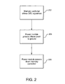
- FIG. 2 shows a flow diagram of the procedure for powering down memory circuitry 100 of FIG. 1 , according to one embodiment of the present invention.
- memory controller 104 drives the CKE signal low, thereby placing memory device 102 in self-refresh mode.
- power module 106 powers the termination voltage Vttcke down to ground.
- power module 106 powers down memory controller 104.
- memory circuitry 100 ensures that memory device 102 stays in self-refresh mode while memory controller 104 is powered down and as long as memory controller 104 remains powered off.
- power module 102 maintains DRAM power lines 112 at their normal operating levels, and reset controller 108 maintains (active low) reset signal 116 at a high level. This enables memory controller 104 to be completely powered off.
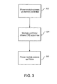
- FIG. 3 shows a flow diagram of the procedure for powering up memory circuitry 100 of FIG. 1 following the power-down procedure of FIG. 2 , according to one embodiment of the present invention.
- power module 106 powers up memory controller 104.
- memory controller 104 drives the CKE signal low, which is the initial default setting for power-on reset.
- power module 106 powers up the termination voltage Vttcke.
- memory circuitry 100 ensures that memory device 102 stays in self-refresh mode until memory controller 104 is powered up and able to resume control over the operations of memory device 102.
- power module 106 maintains DRAM power lines 112 at their normal operating levels, and reset controller 108 maintains reset signal 116 at a high level.
- the present invention has been described in the context of memory circuitry 100 of FIG. 1 having a single DDR3 RDIMM memory device, it will be understood that, in general, the present invention can be implemented for any suitable type of memory topology having one or more memory devices, where those memory devices can be RDIMMs, such as DDR1, DDR2, or DDR3 RDIMMs, or other suitable on-board devices.
- the present invention may be implemented as (analog, digital, or a hybrid of both analog and digital) circuit-based processes, including possible implementation as a single integrated circuit (such as an ASIC or an FPGA), a multi-chip module, a single card, or a multi-card circuit pack.
- a single integrated circuit such as an ASIC or an FPGA
- a multi-chip module such as a single card, or a multi-card circuit pack.
- various functions of circuit elements may also be implemented as processing blocks in a software program.
- Such software may be employed in, for example, a digital signal processor, micro-controller, or general-purpose computer.
- Couple refers to any manner known in the art or later developed in which energy is allowed to be transferred between two or more elements, and the interposition of one or more additional elements is contemplated, although not required. Conversely, the terms “directly coupled,” “directly connected,” etc., imply the absence of such additional elements.
- figure numbers and/or figure reference labels in the claims is intended to identify one or more possible embodiments of the claimed subject matter in order to facilitate the interpretation of the claims. Such use is not to be construed as necessarily limiting the scope of those claims to the embodiments shown in the corresponding figures.
Landscapes
- Engineering & Computer Science (AREA)
- Microelectronics & Electronic Packaging (AREA)
- Computer Hardware Design (AREA)
- Theoretical Computer Science (AREA)
- Power Engineering (AREA)
- Physics & Mathematics (AREA)
- General Engineering & Computer Science (AREA)
- General Physics & Mathematics (AREA)
- Dram (AREA)
- Memory System (AREA)
- Power Sources (AREA)
- Techniques For Improving Reliability Of Storages (AREA)
Abstract
Description
- The present invention relates to electronics, and, in particular, to memory devices having self-refresh modes.
- In typical computer hardware architectures, an integrated circuit (IC) memory device chip is controlled by a separate IC memory controller chip that controls the writing of data to and the reading of data from the memory device during normal operations of the memory device. Some memory devices are capable of operating in a self-refresh mode in which the memory device maintains its stored data even when the memory controller is powered off.
- For some memory devices, such as DDR1 and DDR2 registered dual in-line memory modules (RDIMMs), where DDR stands for "double data rate," the memory device's RESET signal can be used to keep the memory device in self-refresh mode by holding the memory device's clock enable (CKE) line low while allowing the memory controller to be powered down. For other memory devices, such as DDR3 RDIMM memory devices, asserting the RESET signal takes the memory device out of self-refresh mode. As such, when the memory controller is powered off, the RESET signal cannot be used to keep the memory device in self-refresh mode, thereby jeopardizing the integrity of the data stored in the memory device.
- In one embodiment, the present invention is a method for operating memory circuitry having a memory device, a memory controller, and a power module. The memory controller controls normal operations of the memory device by applying a clock enable (CKE) signal to a CKE input of the memory device, wherein the CKE input is further connected to a CKE termination node powered to a CKE termination voltage by the power module. The memory controller is then powered down by (1) the memory controller driving the CKE signal low, (2) then the power module powering down the CKE termination voltage, and (3) then the power module powering down the memory controller.
- In another embodiment, the present invention is a circuitry comprising (1) a memory device having a CKE input, (2) a memory controller connected to apply a CKE signal to the CKE input, and (3) a power module connected to apply a CKE termination voltage to a CKE termination node connected to the CKE input. During normal operations, the memory controller applies the CKE signal to the CKE input with the power module applying the CKE termination voltage to the CKE termination node. During power-down operations, the memory controller drives the CKE signal low, followed by the power module powering down the CKE termination voltage, followed by the power module powering down the memory controller.
- In yet another embodiment, the present invention is a power module for circuitry comprising a memory device having a CKE input and a memory controller connected to apply a CKE signal to the CKE input. The power module is adapted to be connected to apply a CKE termination voltage to a CKE termination node connected to the CKE input. During normal operations, the memory controller applies the CKE signal to the CKE input with the power module applying the CKE termination voltage to the CKE termination node. During power-down operations, the memory controller drives the CKE signal low, followed by the power module powering down the CKE termination voltage, followed by the power module powering down the memory controller.
- Other aspects, features, and advantages of the present invention will become more fully apparent from the following detailed description, the appended claims, and the accompanying drawings in which like reference numerals identify similar or identical elements.
-
FIG. 1 shows a simplified block diagram of memory circuitry according to one embodiment of the present invention; -
FIG. 2 shows a flow diagram of the procedure for powering down the memory circuitry ofFIG. 1 , according to one embodiment of the present invention; and -
FIG. 3 shows a flow diagram of the procedure for powering up the memory circuitry ofFIG. 1 following the power-down procedure ofFIG. 2 , according to one embodiment of the present invention. - As used in this specification, the term "powered off" refers to a state of an integrated circuit (IC) chip in which no power is applied to the chip. The term "powered on" refers to a state in which power is applied to the chip. The term "powering up" refers to a transition from the powered-off state to the powered-on state, while the term "powering down" refers to a transition from the powered-on state to the powered-off state.
-
FIG. 1 shows a simplified block diagram of memory circuitry 100, according to one embodiment of the present invention. Memory circuitry 100 includes DDR3RDIMM memory device 102,memory controller 104,power module 106,reset controller 108, andtermination resistor 110.Memory controller 104 controls the writing of data to and the reading of data frommemory device 102.Power module 106 provides power tomemory device 102 andmemory controller 104 viapower lines 112 andpower lines 114, respectively. In addition,power module 106 provides termination voltage Vttcke totermination resistor 110, wherepower module 106 is capable of powering down the termination voltage Vttcke, while maintaining the otherDRAM power lines 112 powered on. InFIG. 1 , Vttcke refers to both a termination node and to the termination voltage applied to that termination node bypower module 106.Reset controller 108 applies (active low)reset signal 116 to resetmemory device 102. - In addition to many different signals that are not shown in
FIG. 1 ,memory controller 104 applies clock enable signal CKE to CKE input 118 ofmemory device 102. In order formemory controller 104 to be able to write data to and read data frommemory device 102, the CKE signal must be high. As shown inFIG. 1 , in addition to being connected to the CKE signal frommemory controller 104, CKE input 118 ofmemory device 102 is also connected to the termination voltage Vttcke frompower module 106 viatermination resistor 110. - In one implementation, each element shown in
FIG. 1 , includingtermination resistor 110, is a discrete electronic module mounted on a circuit board and interconnected via suitable board traces.Memory controller 104 may be part of a larger integrated circuit module that provides, in addition to the control ofmemory device 102, other functions related to other system elements not shown inFIG. 1 . Similarly,power module 106 may provide power to other system elements not shown inFIG. 1 , including other memory devices. -
FIG. 2 shows a flow diagram of the procedure for powering down memory circuitry 100 ofFIG. 1 , according to one embodiment of the present invention. Instep 202,memory controller 104 drives the CKE signal low, thereby placingmemory device 102 in self-refresh mode. Instep 204,power module 106 powers the termination voltage Vttcke down to ground. Instep 206,power module 106 powers downmemory controller 104. By holding the termination voltage Vttcke low, memory circuitry 100 ensures thatmemory device 102 stays in self-refresh mode whilememory controller 104 is powered down and as long asmemory controller 104 remains powered off. Note that, during the entire procedure ofFIG. 2 ,power module 102 maintainsDRAM power lines 112 at their normal operating levels, andreset controller 108 maintains (active low)reset signal 116 at a high level. This enablesmemory controller 104 to be completely powered off. -
FIG. 3 shows a flow diagram of the procedure for powering up memory circuitry 100 ofFIG. 1 following the power-down procedure ofFIG. 2 , according to one embodiment of the present invention. Instep 302,power module 106 powers upmemory controller 104. Instep 304,memory controller 104 drives the CKE signal low, which is the initial default setting for power-on reset. Instep 306,power module 106 powers up the termination voltage Vttcke. By holding the termination voltage Vttcke low, memory circuitry 100 ensures thatmemory device 102 stays in self-refresh mode untilmemory controller 104 is powered up and able to resume control over the operations ofmemory device 102. Here, too, during the entire procedure ofFIG. 3 ,power module 106 maintainsDRAM power lines 112 at their normal operating levels, andreset controller 108 maintainsreset signal 116 at a high level. - Although the present invention has been described in the context of memory circuitry 100 of
FIG. 1 havingtermination resistor 110, it will be understood that other suitable types and combinations of impedance devices can be used to connect the CKE input of the memory device to a suitable termination voltage. - Although the present invention has been described in the context of memory circuitry 100 of
FIG. 1 having a single DDR3 RDIMM memory device, it will be understood that, in general, the present invention can be implemented for any suitable type of memory topology having one or more memory devices, where those memory devices can be RDIMMs, such as DDR1, DDR2, or DDR3 RDIMMs, or other suitable on-board devices. - The present invention may be implemented as (analog, digital, or a hybrid of both analog and digital) circuit-based processes, including possible implementation as a single integrated circuit (such as an ASIC or an FPGA), a multi-chip module, a single card, or a multi-card circuit pack. As would be apparent to one skilled in the art, various functions of circuit elements may also be implemented as processing blocks in a software program. Such software may be employed in, for example, a digital signal processor, micro-controller, or general-purpose computer.
- Also for purposes of this description, the terms "couple," "coupling," "coupled," "connect," "connecting," or "connected" refer to any manner known in the art or later developed in which energy is allowed to be transferred between two or more elements, and the interposition of one or more additional elements is contemplated, although not required. Conversely, the terms "directly coupled," "directly connected," etc., imply the absence of such additional elements.
- It will be further understood that various changes in the details, materials, and arrangements of the parts which have been described and illustrated in order to explain the nature of this invention may be made by those skilled in the art without departing from the scope of the invention as expressed in the following claims.
- The use of figure numbers and/or figure reference labels in the claims is intended to identify one or more possible embodiments of the claimed subject matter in order to facilitate the interpretation of the claims. Such use is not to be construed as necessarily limiting the scope of those claims to the embodiments shown in the corresponding figures.
- It should be understood that the steps of the exemplary methods set forth herein are not necessarily required to be performed in the order described, and the order of the steps of such methods should be understood to be merely exemplary. Likewise, additional steps may be included in such methods, and certain steps may be omitted or combined, in methods consistent with various embodiments of the present invention.
- Although the elements in the following method claims, if any, are recited in a particular sequence with corresponding labeling, unless the claim recitations otherwise imply a particular sequence for implementing some or all of those elements, those elements are not necessarily intended to be limited to being implemented in that particular sequence.
- Reference herein to "one embodiment" or "an embodiment" means that a particular feature, structure, or characteristic described in connection with the embodiment can be included in at least one embodiment of the invention. The appearances of the phrase "in one embodiment" in various places in the specification are not necessarily all referring to the same embodiment, nor are separate or alternative embodiments necessarily mutually exclusive of other embodiments. The same applies to the term "implementation."
Claims (15)
- A method for operating memory circuitry having a memory device, a memory controller, and a power module, the method comprising:(a) the memory controller controlling normal operations of the memory device by applying a clock enable (CKE) signal to a CKE input of the memory device, wherein the CKE input is further connected to a CKE termination node powered to a CKE termination voltage by the power module; and(b) then powering down the memory controller by:(b1) the memory controller driving the CKE signal low;(b2) then the power module powering down the CKE termination voltage; and(b3) then the power module powering down the memory controller.
- The invention of claim 1, further comprising:(c) then powering up the memory controller by:(c1) the power module powering up the memory controller;(c2) then the memory controller driving the CKE signal low; and(c3) then the power module powering up the CKE termination voltage.
- The invention of claim 1, wherein the memory device is a registered dual in-line memory module (RDIMM).
- The invention of claim 3, wherein the RDIMM memory device is a double-data-rate three (DDR3) RDIMM memory device.
- The invention of claim 1, wherein the power module applies one or more other voltages to the memory device, wherein, in step (b2), the power module powers down the CKE termination voltage while maintaining the one or more other voltages powered on.
- The invention of claim 1, wherein the CKE termination node is connected to the CKE input via a resistor.
- The invention of claim 1, wherein:the method further comprises (c) then powering up the memory controller by:(c1) the power module powering up the memory controller;(c2) then the memory controller driving the CKE signal low; and
(c3) then the power module powering up the CKE termination voltage;the power module applies one or more other voltages to the memory device, wherein, in step (b2), the power module powers down the CKE termination voltage while maintaining the one or more other voltages powered on; andthe CKE termination node is connected to the CKE input via a resistor. - Circuitry comprising:a memory device having a clock enable (CKE) input;a memory controller connected to apply a CKE signal to the CKE input; anda power module connected to apply a CKE termination voltage to a CKE termination node connected to the CKE input, wherein:during normal operations, the memory controller applies the CKE signal to the CKE input with the power module applying the CKE termination voltage to the CKE termination node; andduring power-down operations, the memory controller drives the CKE signal low, followed by the power module powering down the CKE termination voltage, followed by the power module powering down the memory controller.
- The invention of claim 8, wherein, during power-up operations, the power module powers up the memory controller, followed by the memory controller driving the CKE signal low, followed by the power module powering up the CKE termination voltage.
- The invention of claim 8, wherein the memory device is a registered dual in-line memory module (RDIMM).
- The invention of claim 10, wherein the RDIMM memory device is a double-data-rate three (DDR3) RDIMM memory device.
- The invention of claim 8, wherein the power module is adapted to apply one or more other voltages to the memory device, wherein, during the power-down operations, the power module powers down the CKE termination voltage, while maintaining the one or more other voltages powered on.
- The invention of claim 8, further comprising a resistor connected between the CKE input and the CKE termination node.
- The invention of claim 8, wherein:during power-up operations, the power module powers up the memory controller, followed by the memory controller driving the CKE signal low, followed by the power module powering up the CKE termination voltage;the power module is adapted to apply one or more other voltages to the memory device, wherein, during the power-down operations, the power module powers down the CKE termination voltage, while maintaining the one or more other voltages powered on; andthe circuitry further comprises a resistor connected between the CKE input and the CKE termination node.
- A power module for circuitry comprising a memory device having a clock enable (CKE) input and a memory controller connected to apply a CKE signal to the CKE input, wherein:the power module is adapted to be connected to apply a CKE termination voltage to a CKE termination node connected to the CKE input;during normal operations, the memory controller applies the CKE signal to the CKE input with the power module applying the CKE termination voltage to the CKE termination node; andduring power-down operations, the memory controller drives the CKE signal low, followed by the power module powering down the CKE termination voltage, followed by the power module powering down the memory controller.
Applications Claiming Priority (1)
| Application Number | Priority Date | Filing Date | Title |
|---|---|---|---|
| US12/431,876 US7869300B2 (en) | 2009-04-29 | 2009-04-29 | Memory device control for self-refresh mode |
Publications (1)
| Publication Number | Publication Date |
|---|---|
| EP2246769A1 true EP2246769A1 (en) | 2010-11-03 |
Family
ID=42226108
Family Applications (1)
| Application Number | Title | Priority Date | Filing Date |
|---|---|---|---|
| EP10158253A Withdrawn EP2246769A1 (en) | 2009-04-29 | 2010-03-29 | Memory device control for self-refresh mode |
Country Status (6)
| Country | Link |
|---|---|
| US (1) | US7869300B2 (en) |
| EP (1) | EP2246769A1 (en) |
| JP (1) | JP5590605B2 (en) |
| KR (1) | KR20100118950A (en) |
| CN (1) | CN101882464B (en) |
| TW (1) | TWI527030B (en) |
Cited By (1)
| Publication number | Priority date | Publication date | Assignee | Title |
|---|---|---|---|---|
| US9761301B2 (en) | 2015-08-26 | 2017-09-12 | Canon Kabushiki Kaisha | Memory control circuit for controlling memory device that operates in self-refresh mode, and method of controlling the same |
Families Citing this family (9)
| Publication number | Priority date | Publication date | Assignee | Title |
|---|---|---|---|---|
| WO2012115839A1 (en) * | 2011-02-23 | 2012-08-30 | Rambus Inc. | Protocol for memory power-mode control |
| US9159397B2 (en) | 2012-12-04 | 2015-10-13 | Micron Technology, Inc. | Methods and apparatuses for refreshing memory |
| JP2014146115A (en) * | 2013-01-28 | 2014-08-14 | Canon Inc | Data processing device and control method thereof |
| US10055370B2 (en) * | 2014-07-09 | 2018-08-21 | Advanced Micro Devices, Inc. | Method and apparatis for processor standby |
| US9142280B1 (en) | 2014-08-06 | 2015-09-22 | Freescale Semiconducotr, Inc. | Circuit for configuring external memory |
| JP6712312B2 (en) * | 2015-08-24 | 2020-06-17 | エスアールシー ラボス、エルエルシー | System and method for retaining DRAM data when reprogramming a reconfigurable device with a DRAM memory controller incorporating a data maintenance block co-located with a memory module or subsystem |
| KR102535182B1 (en) | 2016-07-27 | 2023-05-23 | 에스케이하이닉스 주식회사 | Semiconductor device |
| US11176986B2 (en) * | 2019-12-30 | 2021-11-16 | Advanced Micro Devices, Inc. | Memory context restore, reduction of boot time of a system on a chip by reducing double data rate memory training |
| TWI897241B (en) * | 2024-02-19 | 2025-09-11 | 華邦電子股份有限公司 | Memory storage apparatus and method for operating memory storage apparatus |
Citations (3)
| Publication number | Priority date | Publication date | Assignee | Title |
|---|---|---|---|---|
| US20020144166A1 (en) * | 2001-04-02 | 2002-10-03 | Nai-Shung Chang | Motherboard with reduced power consumption |
| US20060047985A1 (en) | 2004-08-31 | 2006-03-02 | Canon Kabushiki Kaisha | Data storage apparatus and control method thereof |
| US20080031073A1 (en) | 2006-08-07 | 2008-02-07 | Qimonda Ag | Memory Module and Method for Operating the Same |
Family Cites Families (14)
| Publication number | Priority date | Publication date | Assignee | Title |
|---|---|---|---|---|
| US5831467A (en) * | 1991-11-05 | 1998-11-03 | Monolithic System Technology, Inc. | Termination circuit with power-down mode for use in circuit module architecture |
| US6564329B1 (en) * | 1999-03-16 | 2003-05-13 | Linkup Systems Corporation | System and method for dynamic clock generation |
| US6829677B1 (en) * | 2000-05-18 | 2004-12-07 | International Business Machines Corporation | Method and apparatus for preserving the contents of synchronous DRAM through system reset |
| JP3799251B2 (en) * | 2001-08-24 | 2006-07-19 | エルピーダメモリ株式会社 | Memory device and memory system |
| KR100502664B1 (en) * | 2003-04-29 | 2005-07-20 | 주식회사 하이닉스반도체 | On Die Termination Mode Conversion Circuit and its Method |
| KR100529033B1 (en) * | 2003-05-23 | 2005-11-17 | 주식회사 하이닉스반도체 | Synchronous semiconductor memory device |
| KR100528164B1 (en) * | 2004-02-13 | 2005-11-15 | 주식회사 하이닉스반도체 | On die termination mode transfer circuit in semiconductor memory device and its method |
| US7164611B2 (en) * | 2004-10-26 | 2007-01-16 | Micron Technology, Inc. | Data retention kill function |
| JP4775141B2 (en) * | 2005-09-29 | 2011-09-21 | 株式会社ハイニックスセミコンダクター | Delay locked loop circuit |
| KR100866601B1 (en) * | 2006-12-04 | 2008-11-03 | 삼성전자주식회사 | Apparatus and method for controlling termination resistance of semiconductor device |
| JP2008217890A (en) * | 2007-03-02 | 2008-09-18 | Ricoh Co Ltd | Electronic apparatus, image processing apparatus, and power supply control method |
| US7729191B2 (en) * | 2007-09-06 | 2010-06-01 | Micron Technology, Inc. | Memory device command decoding system and memory device and processor-based system using same |
| JP5200692B2 (en) * | 2007-09-14 | 2013-06-05 | 株式会社リコー | Data processing apparatus, voltage control method for data processing apparatus, and image forming apparatus |
| US7715264B2 (en) * | 2008-06-24 | 2010-05-11 | Qimonda North America Corp. | Method and apparatus for selectively disabling termination circuitry |
-
2009
- 2009-04-29 US US12/431,876 patent/US7869300B2/en active Active
-
2010
- 2010-03-24 TW TW099108749A patent/TWI527030B/en not_active IP Right Cessation
- 2010-03-29 EP EP10158253A patent/EP2246769A1/en not_active Withdrawn
- 2010-04-26 JP JP2010100474A patent/JP5590605B2/en not_active Expired - Fee Related
- 2010-04-28 CN CN201010171270.0A patent/CN101882464B/en not_active Expired - Fee Related
- 2010-04-28 KR KR1020100039348A patent/KR20100118950A/en not_active Ceased
Patent Citations (3)
| Publication number | Priority date | Publication date | Assignee | Title |
|---|---|---|---|---|
| US20020144166A1 (en) * | 2001-04-02 | 2002-10-03 | Nai-Shung Chang | Motherboard with reduced power consumption |
| US20060047985A1 (en) | 2004-08-31 | 2006-03-02 | Canon Kabushiki Kaisha | Data storage apparatus and control method thereof |
| US20080031073A1 (en) | 2006-08-07 | 2008-02-07 | Qimonda Ag | Memory Module and Method for Operating the Same |
Cited By (1)
| Publication number | Priority date | Publication date | Assignee | Title |
|---|---|---|---|---|
| US9761301B2 (en) | 2015-08-26 | 2017-09-12 | Canon Kabushiki Kaisha | Memory control circuit for controlling memory device that operates in self-refresh mode, and method of controlling the same |
Also Published As
| Publication number | Publication date |
|---|---|
| CN101882464B (en) | 2013-10-30 |
| JP5590605B2 (en) | 2014-09-17 |
| US7869300B2 (en) | 2011-01-11 |
| JP2010262645A (en) | 2010-11-18 |
| CN101882464A (en) | 2010-11-10 |
| TWI527030B (en) | 2016-03-21 |
| TW201044391A (en) | 2010-12-16 |
| KR20100118950A (en) | 2010-11-08 |
| US20100278000A1 (en) | 2010-11-04 |
Similar Documents
| Publication | Publication Date | Title |
|---|---|---|
| US7869300B2 (en) | Memory device control for self-refresh mode | |
| US8879348B2 (en) | Power management in semiconductor memory system | |
| US8923088B2 (en) | Solid state storage device with sleep control circuit | |
| EP2472409B1 (en) | Input-output module, and method for extending a memory interface for input-output operations | |
| US20190034106A1 (en) | Power down mode for universal flash storage (ufs) | |
| US7342411B2 (en) | Dynamic on-die termination launch latency reduction | |
| WO2008075292A2 (en) | Power-on temperature sensor/spd detect | |
| CN107667326B (en) | Power management in dual memory platforms | |
| US7698527B2 (en) | Selectively supporting different memory technologies on a single motherboard | |
| US8139433B2 (en) | Memory device control for self-refresh mode | |
| US20080126816A1 (en) | Apparatus and method for switching an apparatus to a power saving mode | |
| JP2744738B2 (en) | Semiconductor storage device | |
| JP2021012688A (en) | Ddr5 client pmic power up sequence and state transitions | |
| CN110633166B (en) | Reset device and reset method | |
| CN103092783B (en) | Memory system | |
| CN104516684A (en) | Data processing system, microcontroller and semiconductor device | |
| US11380378B1 (en) | Clock driver and memory device comprising the same | |
| US7196944B2 (en) | Voltage detection circuit control device, memory control device with the same, and memory card with the same | |
| CN112650384B (en) | Low-power consumption dormancy awakening control circuit and multi-power-domain control circuit | |
| US20110258492A1 (en) | Device for testing serial interface | |
| US9405339B1 (en) | Power controller | |
| US7986580B2 (en) | Self-refresh based power saving circuit and method | |
| US7519841B2 (en) | Power control circuit | |
| US20070205805A1 (en) | Electrical system including driver that provides a first drive strength and a second drive strength | |
| US20090091963A1 (en) | Memory device |
Legal Events
| Date | Code | Title | Description |
|---|---|---|---|
| PUAI | Public reference made under article 153(3) epc to a published international application that has entered the european phase |
Free format text: ORIGINAL CODE: 0009012 |
|
| AK | Designated contracting states |
Kind code of ref document: A1 Designated state(s): AT BE BG CH CY CZ DE DK EE ES FI FR GB GR HR HU IE IS IT LI LT LU LV MC MK MT NL NO PL PT RO SE SI SK SM TR |
|
| AX | Request for extension of the european patent |
Extension state: AL BA ME RS |
|
| RIN1 | Information on inventor provided before grant (corrected) |
Inventor name: KRIZ, JOHN C Inventor name: BHAKTA, DHARMESHKUMAR N Inventor name: PERSSON, ERIC D |
|
| 17P | Request for examination filed |
Effective date: 20110503 |
|
| 17Q | First examination report despatched |
Effective date: 20130104 |
|
| GRAP | Despatch of communication of intention to grant a patent |
Free format text: ORIGINAL CODE: EPIDOSNIGR1 |
|
| RIC1 | Information provided on ipc code assigned before grant |
Ipc: G11C 8/18 20060101ALI20160201BHEP Ipc: G11C 5/04 20060101ALI20160201BHEP Ipc: G06F 1/32 20060101ALI20160201BHEP Ipc: G11C 5/14 20060101ALI20160201BHEP Ipc: G11C 11/406 20060101ALI20160201BHEP Ipc: G11C 11/4076 20060101AFI20160201BHEP Ipc: G11C 5/06 20060101ALI20160201BHEP |
|
| GRAJ | Information related to disapproval of communication of intention to grant by the applicant or resumption of examination proceedings by the epo deleted |
Free format text: ORIGINAL CODE: EPIDOSDIGR1 |
|
| GRAP | Despatch of communication of intention to grant a patent |
Free format text: ORIGINAL CODE: EPIDOSNIGR1 |
|
| INTG | Intention to grant announced |
Effective date: 20160222 |
|
| INTG | Intention to grant announced |
Effective date: 20160321 |
|
| GRAJ | Information related to disapproval of communication of intention to grant by the applicant or resumption of examination proceedings by the epo deleted |
Free format text: ORIGINAL CODE: EPIDOSDIGR1 |
|
| GRAP | Despatch of communication of intention to grant a patent |
Free format text: ORIGINAL CODE: EPIDOSNIGR1 |
|
| INTG | Intention to grant announced |
Effective date: 20160805 |
|
| STAA | Information on the status of an ep patent application or granted ep patent |
Free format text: STATUS: GRANT OF PATENT IS INTENDED |
|
| STAA | Information on the status of an ep patent application or granted ep patent |
Free format text: STATUS: THE APPLICATION IS DEEMED TO BE WITHDRAWN |
|
| 18D | Application deemed to be withdrawn |
Effective date: 20161216 |