EP2245454B1 - Mikroelektroden-array auf basis optisch transparenter leitfähiger polymermaterialien und verfahren zur herstellung davon - Google Patents
Mikroelektroden-array auf basis optisch transparenter leitfähiger polymermaterialien und verfahren zur herstellung davon Download PDFInfo
- Publication number
- EP2245454B1 EP2245454B1 EP09714556.9A EP09714556A EP2245454B1 EP 2245454 B1 EP2245454 B1 EP 2245454B1 EP 09714556 A EP09714556 A EP 09714556A EP 2245454 B1 EP2245454 B1 EP 2245454B1
- Authority
- EP
- European Patent Office
- Prior art keywords
- electrode
- micro
- array
- areas
- sub
- Prior art date
- Legal status (The legal status is an assumption and is not a legal conclusion. Google has not performed a legal analysis and makes no representation as to the accuracy of the status listed.)
- Not-in-force
Links
- 238000000034 method Methods 0.000 title claims description 28
- 238000004519 manufacturing process Methods 0.000 title claims description 22
- 239000004020 conductor Substances 0.000 title description 5
- 239000000758 substrate Substances 0.000 claims description 32
- 239000000463 material Substances 0.000 claims description 28
- 239000011347 resin Substances 0.000 claims description 27
- 229920005989 resin Polymers 0.000 claims description 27
- -1 polydimethylsiloxane Polymers 0.000 claims description 17
- 239000004205 dimethyl polysiloxane Substances 0.000 claims description 16
- 229920000435 poly(dimethylsiloxane) Polymers 0.000 claims description 16
- 229920001609 Poly(3,4-ethylenedioxythiophene) Polymers 0.000 claims description 9
- 238000000820 replica moulding Methods 0.000 claims description 7
- 238000004132 cross linking Methods 0.000 claims description 6
- 238000000151 deposition Methods 0.000 claims description 6
- 239000011521 glass Substances 0.000 claims description 6
- 238000012545 processing Methods 0.000 claims description 6
- 230000000638 stimulation Effects 0.000 claims description 6
- 230000008021 deposition Effects 0.000 claims description 4
- 239000011810 insulating material Substances 0.000 claims description 4
- 230000008569 process Effects 0.000 claims description 4
- 239000007788 liquid Substances 0.000 claims description 3
- 239000000523 sample Substances 0.000 claims description 3
- QVGXLLKOCUKJST-UHFFFAOYSA-N atomic oxygen Chemical compound [O] QVGXLLKOCUKJST-UHFFFAOYSA-N 0.000 claims description 2
- 238000009792 diffusion process Methods 0.000 claims description 2
- 238000011049 filling Methods 0.000 claims description 2
- 239000001301 oxygen Substances 0.000 claims description 2
- 229910052760 oxygen Inorganic materials 0.000 claims description 2
- 239000012472 biological sample Substances 0.000 claims 2
- 230000001766 physiological effect Effects 0.000 claims 2
- 238000007789 sealing Methods 0.000 claims 1
- 238000000926 separation method Methods 0.000 claims 1
- 238000003491 array Methods 0.000 description 17
- 210000004027 cell Anatomy 0.000 description 7
- 229920000642 polymer Polymers 0.000 description 6
- XUIMIQQOPSSXEZ-UHFFFAOYSA-N Silicon Chemical compound [Si] XUIMIQQOPSSXEZ-UHFFFAOYSA-N 0.000 description 4
- 238000004113 cell culture Methods 0.000 description 4
- 229920001940 conductive polymer Polymers 0.000 description 4
- 238000005516 engineering process Methods 0.000 description 4
- 238000010438 heat treatment Methods 0.000 description 4
- 238000005286 illumination Methods 0.000 description 4
- 229910052710 silicon Inorganic materials 0.000 description 4
- 239000010703 silicon Substances 0.000 description 4
- 238000004458 analytical method Methods 0.000 description 3
- 210000004413 cardiac myocyte Anatomy 0.000 description 3
- 238000004049 embossing Methods 0.000 description 3
- 238000000386 microscopy Methods 0.000 description 3
- 239000000203 mixture Substances 0.000 description 3
- BASFCYQUMIYNBI-UHFFFAOYSA-N platinum Chemical compound [Pt] BASFCYQUMIYNBI-UHFFFAOYSA-N 0.000 description 3
- 238000007781 pre-processing Methods 0.000 description 3
- KDLHZDBZIXYQEI-UHFFFAOYSA-N Palladium Chemical compound [Pd] KDLHZDBZIXYQEI-UHFFFAOYSA-N 0.000 description 2
- 239000004642 Polyimide Substances 0.000 description 2
- 229910052581 Si3N4 Inorganic materials 0.000 description 2
- VYPSYNLAJGMNEJ-UHFFFAOYSA-N Silicium dioxide Chemical compound O=[Si]=O VYPSYNLAJGMNEJ-UHFFFAOYSA-N 0.000 description 2
- 230000003321 amplification Effects 0.000 description 2
- 210000004556 brain Anatomy 0.000 description 2
- 230000009977 dual effect Effects 0.000 description 2
- 238000001914 filtration Methods 0.000 description 2
- 210000002569 neuron Anatomy 0.000 description 2
- 238000003199 nucleic acid amplification method Methods 0.000 description 2
- 238000000059 patterning Methods 0.000 description 2
- 229920003229 poly(methyl methacrylate) Polymers 0.000 description 2
- 229920001721 polyimide Polymers 0.000 description 2
- 239000004926 polymethyl methacrylate Substances 0.000 description 2
- 238000007639 printing Methods 0.000 description 2
- 238000007650 screen-printing Methods 0.000 description 2
- HQVNEWCFYHHQES-UHFFFAOYSA-N silicon nitride Chemical compound N12[Si]34N5[Si]62N3[Si]51N64 HQVNEWCFYHHQES-UHFFFAOYSA-N 0.000 description 2
- 210000002237 B-cell of pancreatic islet Anatomy 0.000 description 1
- 229920000144 PEDOT:PSS Polymers 0.000 description 1
- ATJFFYVFTNAWJD-UHFFFAOYSA-N Tin Chemical compound [Sn] ATJFFYVFTNAWJD-UHFFFAOYSA-N 0.000 description 1
- RTAQQCXQSZGOHL-UHFFFAOYSA-N Titanium Chemical group [Ti] RTAQQCXQSZGOHL-UHFFFAOYSA-N 0.000 description 1
- 230000009471 action Effects 0.000 description 1
- 238000000137 annealing Methods 0.000 description 1
- 230000008827 biological function Effects 0.000 description 1
- 230000000747 cardiac effect Effects 0.000 description 1
- 230000019522 cellular metabolic process Effects 0.000 description 1
- 238000006243 chemical reaction Methods 0.000 description 1
- 229910052681 coesite Inorganic materials 0.000 description 1
- 229910052906 cristobalite Inorganic materials 0.000 description 1
- 238000010586 diagram Methods 0.000 description 1
- HTXDPTMKBJXEOW-UHFFFAOYSA-N dioxoiridium Chemical compound O=[Ir]=O HTXDPTMKBJXEOW-UHFFFAOYSA-N 0.000 description 1
- 238000001035 drying Methods 0.000 description 1
- 238000004070 electrodeposition Methods 0.000 description 1
- 230000007831 electrophysiology Effects 0.000 description 1
- 238000002001 electrophysiology Methods 0.000 description 1
- 229920005570 flexible polymer Polymers 0.000 description 1
- 230000006870 function Effects 0.000 description 1
- PCHJSUWPFVWCPO-UHFFFAOYSA-N gold Chemical compound [Au] PCHJSUWPFVWCPO-UHFFFAOYSA-N 0.000 description 1
- 229910052737 gold Inorganic materials 0.000 description 1
- 239000010931 gold Substances 0.000 description 1
- 231100001261 hazardous Toxicity 0.000 description 1
- 239000007943 implant Substances 0.000 description 1
- 238000001727 in vivo Methods 0.000 description 1
- 229910003437 indium oxide Inorganic materials 0.000 description 1
- PJXISJQVUVHSOJ-UHFFFAOYSA-N indium(iii) oxide Chemical compound [O-2].[O-2].[O-2].[In+3].[In+3] PJXISJQVUVHSOJ-UHFFFAOYSA-N 0.000 description 1
- 238000007641 inkjet printing Methods 0.000 description 1
- 230000010354 integration Effects 0.000 description 1
- 230000003993 interaction Effects 0.000 description 1
- 229910052741 iridium Inorganic materials 0.000 description 1
- GKOZUEZYRPOHIO-UHFFFAOYSA-N iridium atom Chemical compound [Ir] GKOZUEZYRPOHIO-UHFFFAOYSA-N 0.000 description 1
- 229910000457 iridium oxide Inorganic materials 0.000 description 1
- 239000002207 metabolite Substances 0.000 description 1
- 229910052751 metal Inorganic materials 0.000 description 1
- 239000002184 metal Substances 0.000 description 1
- 239000007769 metal material Substances 0.000 description 1
- 238000003801 milling Methods 0.000 description 1
- 238000012986 modification Methods 0.000 description 1
- 230000004048 modification Effects 0.000 description 1
- 238000000465 moulding Methods 0.000 description 1
- 230000001537 neural effect Effects 0.000 description 1
- 235000016709 nutrition Nutrition 0.000 description 1
- 230000035764 nutrition Effects 0.000 description 1
- 210000000056 organ Anatomy 0.000 description 1
- 229920000620 organic polymer Polymers 0.000 description 1
- 229910052763 palladium Inorganic materials 0.000 description 1
- 230000002093 peripheral effect Effects 0.000 description 1
- 210000001428 peripheral nervous system Anatomy 0.000 description 1
- 229910052697 platinum Inorganic materials 0.000 description 1
- 230000005855 radiation Effects 0.000 description 1
- 230000003252 repetitive effect Effects 0.000 description 1
- 230000000717 retained effect Effects 0.000 description 1
- 230000002207 retinal effect Effects 0.000 description 1
- 150000003839 salts Chemical class 0.000 description 1
- 238000005070 sampling Methods 0.000 description 1
- 239000000377 silicon dioxide Substances 0.000 description 1
- 238000000935 solvent evaporation Methods 0.000 description 1
- 238000004528 spin coating Methods 0.000 description 1
- 238000004544 sputter deposition Methods 0.000 description 1
- 229910052682 stishovite Inorganic materials 0.000 description 1
- 239000000126 substance Substances 0.000 description 1
- 229910001887 tin oxide Inorganic materials 0.000 description 1
- 239000010936 titanium Substances 0.000 description 1
- OGIDPMRJRNCKJF-UHFFFAOYSA-N titanium oxide Inorganic materials [Ti]=O OGIDPMRJRNCKJF-UHFFFAOYSA-N 0.000 description 1
- 230000026683 transduction Effects 0.000 description 1
- 238000010361 transduction Methods 0.000 description 1
- 239000012780 transparent material Substances 0.000 description 1
- 229910052905 tridymite Inorganic materials 0.000 description 1
- 238000001947 vapour-phase growth Methods 0.000 description 1
- 238000005406 washing Methods 0.000 description 1
Images


Classifications
-
- G—PHYSICS
- G01—MEASURING; TESTING
- G01N—INVESTIGATING OR ANALYSING MATERIALS BY DETERMINING THEIR CHEMICAL OR PHYSICAL PROPERTIES
- G01N33/00—Investigating or analysing materials by specific methods not covered by groups G01N1/00 - G01N31/00
- G01N33/48—Biological material, e.g. blood, urine; Haemocytometers
- G01N33/483—Physical analysis of biological material
- G01N33/4833—Physical analysis of biological material of solid biological material, e.g. tissue samples, cell cultures
- G01N33/4836—Physical analysis of biological material of solid biological material, e.g. tissue samples, cell cultures using multielectrode arrays
Definitions
- the present invention relates to a micro-electrode array, and to the corresponding manufacturing technique.
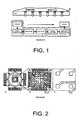
- FIG. 1 A schematic representation of the acquisition and/or stimulation of bioelectric signals through a micro-electrode array is shown in Fig. 1 .
- the micro-electrode arrays can essentially act according to two "dual” modes, detecting bioelectric signals emitted by a biological entity, or delivering preset electric pulses to influence biologic functions, respectively. They are considered “non-invasive” devices, since they do not penetrate the cells, thus damaging them, but they simply act by virtue of a contact.
- the bioelectric signals are detected in the form of capacitive currents which are drawn at microscopic contact terminals located in an interaction area with the biological entity to be analyzed, and are conducted through interconnection tracks to peripheral macroscopic contact pads, adapted to provide an electric connection with processing, amplification and filtering electronics.
- the preset stimulation voltage or current pulses for the entity under examination can be provided by external generating devices via the contact pads, thereby arriving to the micro-electrodes by covering an inverse path along the interconnection tracks, to stimulate the biological entities in contact therewith.
- Micro-electrode arrays can be employed also for in vivo applications, for example, for the stimulation of organs (deep encephalon, retinal implants), artificial apparatus (cardiac pacemakers), or for the interconnection with the peripheral nervous systems for the control of prostheses.
- recording of the electrophysiological signals can be carried out by two different types of micro-electrode arrays: active arrays or passive arrays.
- the micro-electrode active arrays comprise an electronics for amplification, filtering and/or pre-processing of signals which is integrated with the array.
- these arrays are manufactured in the CMOS or FET technology.
- the main advantages are the arrangement of a high number of micro-electrodes, the integration of the pre-processing electronics, which does not require the use of expensive external equipments, and the possibility of mass manufacturing.
- micro-electrode passive arrays comprise micro-electrodes circuit arrangements used only for the transduction of the bioelectric signals, that is, without further pre-processing. Such arrays are adapted to conduct the bioelectric signals via the interconnection tracks to the outer contact pads, where they are subsequently amplified and analyzed by external electronics.
- passive arrays have a quite simple layout. They consist in a support material on which metal electrode terminals, interconnection tracks, and micromachined contact pads are defined via photolithographic processes, as shown according to an illustration in different scales in Fig. 2 .
- Typical support materials are glass or polymers such as, for example, polyimide.
- vapour phase deposition or screen printing techniques are employed.
- Gold, platinum, palladium, iridium, or tin and indium oxide are the metal materials typically employed as conductors for manufacturing the electrodes.
- the diameters of the micro-electrodes range between 10 and 100 microns, and the spacing therebetween typically ranges between 10 and 500 microns.
- the electrodes are modified by means of a sputtering deposition of titanium or iridium oxide emitters, or by fractal platinum black electrodeposition to enlarge the effective surface area thereof and/or the charge delivery capacity thereof.
- the interconnection conductive tracks which connect the micro-electrodes to the macroscopic contact pads to convey the electric signal from its source to a position in which it is processed or used, are insulated so as to avoid losses of signal in the path between the micro-electrodes and the contact pads.
- Typical insulating materials are glass (SiO 2 ), silicon nitride (Si 3 N 4 ), or non-conductive polymers, such as polyimide.
- the materials constituting the micro-electrode arrays have transparency and biocompatibility properties, typically having to contact a cell culture.
- object of the invention is to manufacture a passive micro-electrode array with transparency and biocompatibility characteristics, at low cost, by providing a relative mass production process which is rapid and also inexpensive, complying with the following constraints:
- micro-electrode array having the characteristics defined by claim 1.
- the present invention is based on the principle of manufacturing a micro-electrode array starting from electrically conductive polymeric materials and electrically insulating polymeric materials which have properties of biocompatibility, biostability, and transparency to light radiation.
- Such materials can be processed by employing a two-layer master mould carrying predetermined microstructures for the fabrication of a substrate of the array, preferably via a replica molding technology.
- the micro-electrode array substrate is made of insulating material, preferably transparent polydimethylsiloxane (PDMS).
- PDMS transparent polydimethylsiloxane
- the conductive materials for the electrodes, the interconnection tracks, and the contact pads are transparent polymeric materials, preferably organic polymeric materials, such as poly(3,4-ethylenedioxythiophene) (PEDOT).
- PEDOT poly(3,4-ethylenedioxythiophene)
- the production process steps for the array can be automated.
- an insulating crosslinkable polymer such as polydimethylsiloxane
- a conductive polymeric liquid such as poly(3,4-ethylenedioxythiophene)
- the remaining open cavities are insulated by a mechanical support layer, for example, obtained by deposition of a second PDMS layer (in order to implement a wholly polymer-based micro-electrode array), or a glass film.
- Such a micro-electrode array is an array of the passive type, since it does not provide for the implementation of signal processing electronic components or circuits.
- Such an array is adapted to transduce and direct biological signals emitted by a microscopic source, for example, a cell culture substrate in contact with the electrode areas of the array, to external macroscopic processing equipments, such as amplifiers, filters, and other data conversion equipments connected via the array connection pads.
- the micro-electrodes thus manufactured have diameters ranging between 10 and 100 micrometers, and the connection pads have dimensions of the order of 1x2mm 2 .
- the array including a substrate of transparent polymer, as well as a plurality of micro-electrodes, a plurality of respective interconnection tracks, and corresponding contact pads of transparent organic conductive polymer, and spaced one from the other by an insulating material based on a transparent polymer.
- a master mould having in the negative the structures of the final micro-electrode array is obtained in a first step ( Figs. 4a-4f ).
- the master mould includes materials which have minimum abrasive properties in order to allow the repetitive moulding of a number of micro-electrode arrays.
- Such a master can be produced, for example, by photolithographic patterning of photosensitive resin layers on a silicon wafer, but other production techniques can be employed, such as, for example, hot embossing or micro-milling techniques.
- the first mask M1 reproduces the array central micro-electrodes, the inter-connection tracks which result buried in the end structure, and the outer contact pads, while the second mask M2 only reproduces the central micro-electrodes and the contact pads which have to result to be as exposed areas in the end structure.
- the image produced in the resin is the negative or positive image of the photomask (for example, in the case of a positive photosensitive resin, the resin illuminated areas are washed off, while the non-illuminated areas are maintained, that is, a positive resin produces a negative image of the mask).
- the illuminated areas are subjected to crosslinking, thereby forming a configuration of relief microstructures which has a height which is equal to the resin layer initial thickness, while the non-illuminated areas are washed off in a successive washing or "development" step.
- a suitably cleaned silicon wafer W ( Fig. 4a ) is coated - by means, for example, of a spin-coating technique - with a first photosensitive resin layer R, for example, having a thickness ranging between 10 and 200 micrometers.
- the resin layer undergoes curing in a two-step heating process comprising, for example, a first heating step at 65 °C for a period of 10 minutes, followed by a second heating step at the temperature of 95 °C for a period of 30 minutes ( Fig. 4b ).
- the first photomask M1 bearing the image of the three conductive components (electrodes, interconnection tracks, and contact pads) of the micro-electrode array is arranged in the cured state on the resin layer R. Then, the structure is subjected to illumination ( Fig. 4c ) with ultraviolet rays to reach a crosslinked condition.
- the illuminated areas stabilize by crosslinking (areas R').
- the resin deposition and crosslinking process is repeated to grow the patterned resin layer ( Figs. 4d, 4e ), this time through the second photomask M2 bearing only the images of the electrodes and the outer contact pads.
- the second mask has to be precisely aligned over the already produced first structure by means of suitable aligning references.
- the second resin layer thickness can be different from the first layer thickness.
- both resin layers are removed ( Fig. 4f ), revealing on the silicon wafer substrate the microstructures S defined by the transparent areas of the two photomasks through the thickness of the two respective resin layers, thus constituting the master mould M for the successive replica molding steps.
- Figs. 5a-5e the manufacturing steps of a micro-electrode array A according to the preferred replica molding technique starting from the thus-manufactured master M, which can be employed for the printing of a virtually infinite number of polymeric micro-electrode arrays are shown in succession.
- a filling step of the mould M through a polydimethylsiloxane (PDMS) pre-polymeric viscous mixture for example, the mixture known under the trade name Sylgard 184 manufactured by Dow Coming, is shown. Then, the mixture is subjected to crosslinking (for example, by heating), and the thus-obtained flexible polymer is peeled off from the master, thereby originating an armature of substrate SUB of the micro-electrode array ( Fig. 5b ) provided with cavities C at the location of the resin microstructures of the mould M.
- PDMS polydimethylsiloxane
- an electrically conductive liquid polymeric solution LP for example, the organic polymer poly(3,4-ethylenedioxythiophene) (PEDOT), known under the trade name Baytron P CPP 105D by Starck/Bayer, and dried by solvent evaporation ( Fig. 5c ).
- PEDOT organic polymer poly(3,4-ethylenedioxythiophene)
- Baytron P CPP 105D Baytron P CPP 105D by Starck/Bayer
- the upper surface of the semi-finished structure constituting the micro-electrode array rear side, is preferably coated ( Fig. 5d ) with an additional PDMS or glass film layer B, deposited by pipetting, screen printing, or ink jet printing, acting as a mechanical support layer for an enhanced stiffness of the array structure on the whole.
- Fig. 5e the completed structure of the micro-electrode array A, obtained by overturning the structure of Fig. 5d , is shown.
- the support layer B, the substrate SUB, the buried interconnection tracks T regions, and the surface electrodes E are shown in cross-section. Then the cells can be cultured on the upper side via standard cell culture protocols.
- Fig. 6 a sectional, enlarged view of the thus-obtained array is shown, in which the conductive portions, emerging to the surface of the substrate SUB, of the micro-electrodes E and the contact pads P, and the buried conductive portions of the conductive tracks T are highlighted.
- the conductors are electrically insulated from the outside, except for the signal source areas or signal withdrawal areas. These areas are arranged at opposite ends of each conductor, one of which being represented by a central micro-electrode E in the proximity of the biological entities BIO to be analyzed, the other one being a macroscopic contact pad P at the array outer edge.
Landscapes
- Health & Medical Sciences (AREA)
- Life Sciences & Earth Sciences (AREA)
- Engineering & Computer Science (AREA)
- Biomedical Technology (AREA)
- Physics & Mathematics (AREA)
- Chemical & Material Sciences (AREA)
- Biochemistry (AREA)
- General Health & Medical Sciences (AREA)
- Molecular Biology (AREA)
- Urology & Nephrology (AREA)
- Optics & Photonics (AREA)
- Food Science & Technology (AREA)
- Hematology (AREA)
- Medicinal Chemistry (AREA)
- Biophysics (AREA)
- Analytical Chemistry (AREA)
- General Physics & Mathematics (AREA)
- Immunology (AREA)
- Pathology (AREA)
- Apparatus Associated With Microorganisms And Enzymes (AREA)
- Non-Insulated Conductors (AREA)
- Devices For Indicating Variable Information By Combining Individual Elements (AREA)
Claims (13)
- Mikroelektroden-Array (A), umfassend ein Isoliersubstrat (SUB) und mehrere darin festgelegte Leiterbahnen (E, T, P), die jeweils einschließen:- einen Elektrodenbereich (E) mit Mikrometerdimensionen, der an der Arrayoberfläche (A) in einer ersten Kontaktregion mit einer zu analysierenden oder zu stimulierenden biologischen Probe zutage tritt;- einen Verbindungsbereich (P) mit makroskopischen Dimensionen, der an der Arrayoberfläche (A) in einer zweiten Kontaktregion für die elektrische Verbindung mit externen Schaltungsanordnungen für Signalverarbeitung zutage tritt, ausgelegt zum Erzeugen elektrischer Stimulationssignale, die dem Elektrodenbereich (E) zuzuführen sind, oder zum Verarbeiten durch den Elektrodenbereich (E) aufgefangener elektrischer Signale, die repräsentativ für die physiologische Probenaktivität sind;- eine vergrabene Region (T) zur gegenseitigen Verbindung, zwischen dem Elektrodenbereich (E) und dem Verbindungsbereich (P),wobei der Array (A) dadurch gekennzeichnet ist, dass das Isoliersubstrat (SUB) aus einem ersten polymeren Material gefertigt ist, und die Leiterbahnen (E, T, P) aus einem zweiten polymeren Material gefertigt sind.
- Mikroelektroden-Array (A) nach Anspruch 1, wobei das erste und das zweite polymere Material optisch transparent sind.
- Mikroelektroden-Array nach Anspruch 2, wobei das isolierende polymere Material Polydimethylsiloxan (PDMS) ist.
- Mikroelektroden-Array (A) nach Anspruch 2, wobei das leitende polymere Material Poly(3,4-ethylendioxythiophen) (PEDOT) ist.
- Mikroelektroden-Array (A) nach einem der vorstehenden Ansprüche, umfassend eine mechanische Trägerschicht (B) für das Substrat (SUB), angeordnet an einem Teil gegenüber der zutage tretenden Fläche der Elektrodenbereiche (E) und der Verbindungsbereiche (P) der Leiterbahnen, wobei die Trägerschicht (B) aus Polydimethylsiloxan (PDMS) gefertigt ist.
- Mikroelektroden-Array (A) nach einem der vorstehenden Ansprüche, umfassend eine mechanische Trägerschicht (B) für das Substrat (SUB), angeordnet an einem Teil gegenüber der zutage tretenden Fläche der Elektrodenbereiche (E) und der Verbindungsbereiche (P) der Leiterbahnen, wobei die Trägerschicht (B) aus Glas gefertigt ist.
- Verfahren für die Herstellung eines Mikroelektroden-Arrays (A), der ein Isoliersubstrat (SUB) und mehrere darin festgelegte Leiterbahnen (E, T, P) umfasst, die jeweils einschließen:- einen Elektrodenbereich (E) mit Mikrometerdimensionen, der an der Arrayoberfläche (A) in einer ersten Kontaktregion mit einer zu analysierenden oder zu stimulierenden biologischen Probe zutage tritt;- einen Verbindungsbereich (P) mit makroskopischen Dimensionen, der an der Arrayoberfläche (A) in einer zweiten Kontaktregion für die elektrische Verbindung mit externen Schaltungsanordnungen für Signalverarbeitung zutage tritt, ausgelegt zum Erzeugen elektrischer Stimulationssignale, die dem Elektrodenbereich (E) zuzuführen sind, oder zum Verarbeiten durch den Elektrodenbereich (E) aufgefangener elektrischer Signale, die repräsentativ für die physiologische Probenaktivität sind;- eine vergrabene Region (T) zur gegenseitigen Verbindung, zwischen dem Elektrodenbereich (E) und dem Verbindungsbereich (P),
wobei das Verfahren die Schritte umfasst:- Konfigurieren eines Isoliersubstrat- (SUB-) Volumens eines ersten polymeren Materials durch eine vorab angeordnete Mutterform (M), die eine Konfiguration von Mikrostrukturen (S) trägt, angepasst zur Festlegung mehrerer Elektrodenbereiche (E), entsprechender Verbindungsbereiche (P) und relativer Regionen (T) zur gegenseitigen Verbindung im Substrat- (SUB-) Volumen, in Form von Kavitäten (C);- Füllen der Kavitäten (C) mit einem zweiten leitenden polymeren Material, um die Leiterbahnen (E, T, P) zu bilden; und- Anordnen einer Isoliermaterial-Abdichtschicht (B) für die gefüllten Kavitäten (C). - Verfahren nach Anspruch 7, wobei die Konfiguration eines Isoliersubstrat- (SUB-) Volumens durch Replica-Molding stattfindet, und die folgenden Schritte einschließt:- Deponierung des ersten Materials in einem präpolymeren viskosen Zustand in der Form (M);- Vernetzung des Materialvolumens;- Trennung des Substrat- (SUB-) Volumens von der Form (M), um Kavitäten (C) zugänglich zu machen, die darin durch die Konfiguration von Reliefmikrostrukturen (S) der Form (M) ausgebildet sind; und- Ausfüllen der Kavitäten (C) mit dem zweiten Material in präpolymerem flüssigem Zustand durch Kapillardiffusion, und sukzessives Aushärten des Materials.
- Verfahren nach Anspruch 7, wobei das isolierende polymere Material Polydimethylsiloxan (PDMS) ist.
- Verfahren nach Anspruch 9, das einen PDMS-Hydrophilierungsschritt mittels eines Sauerstoffplasmas umfasst.
- Verfahren nach Anspruch 7, wobei das leitende polymere Material Poly(3,4-Ethylendioxythiophen) (PEDOT) ist.
- Verfahren nach Anspruch 7, wobei die Mutterform (M) erhalten wird durch photolithographische Strukturierung einer ersten photosensitiven Harzschicht (R) für die Konfiguration vergrabener leitender Bereiche (T) des Arrays (A) und anschließend einer zweiten überlappten photosensitiven Harzschicht (R) für die Konfiguration freiliegender leitender Bereiche (AND, P) des Arrays (A).
- Verfahren nach Anspruch 12, wobei die Herstellung der Mutterform (M) umfasst:- Anordnen eines Trägersubstrats (W);- Aufbringen einer ersten photosensitiven Harzschicht (R) auf das Substrat (W);- Beleuchten der aufgebrachten Harzschicht (R) durch eine erste Photomaske (M1), die das Bild der Elektrodenbereiche (E), entsprechender Verbindungsbereiche (P) und relativer Regionen (T) zur gegenseitigen Verbindung trägt, zwecks Erzielung eines vernetzten Zustands (R');- Aufbringen einer zweiten photosensitiven Harzschicht (R) auf die erste Schicht;- Beleuchten der aufgebrachten Harzschicht (R) durch eine zweite Photomaske (M2), die sich in ausgerichtetem Zustand befindet, und die das Bild der Elektrodenbereiche (E) und entsprechenden Verbindungsbereiche (P) trägt, zwecks Erzielung eines vernetzten Zustands (R'); und- Entwickeln und selektives Entfernen der nicht vernetzten Harzschichten (R), um die Konfiguration von Mikrostrukturen (S) im Relief auf dem Trägersubstrat (W) zu erhalten.
Applications Claiming Priority (2)
| Application Number | Priority Date | Filing Date | Title |
|---|---|---|---|
| IT000152A ITTO20080152A1 (it) | 2008-02-29 | 2008-02-29 | Matrice di microelettrodi a base di materiali conduttori polimerici otticamente trasparenti, e procedimento per la sua fabbricazione |
| PCT/IB2009/050751 WO2009107069A2 (en) | 2008-02-29 | 2009-02-25 | Micro-electrode array based on optically transparent polymeric conductive materials, and method for the manufacturing thereof |
Publications (2)
| Publication Number | Publication Date |
|---|---|
| EP2245454A2 EP2245454A2 (de) | 2010-11-03 |
| EP2245454B1 true EP2245454B1 (de) | 2015-06-24 |
Family
ID=40292025
Family Applications (1)
| Application Number | Title | Priority Date | Filing Date |
|---|---|---|---|
| EP09714556.9A Not-in-force EP2245454B1 (de) | 2008-02-29 | 2009-02-25 | Mikroelektroden-array auf basis optisch transparenter leitfähiger polymermaterialien und verfahren zur herstellung davon |
Country Status (4)
| Country | Link |
|---|---|
| US (1) | US20110001466A1 (de) |
| EP (1) | EP2245454B1 (de) |
| IT (1) | ITTO20080152A1 (de) |
| WO (1) | WO2009107069A2 (de) |
Cited By (2)
| Publication number | Priority date | Publication date | Assignee | Title |
|---|---|---|---|---|
| FR3139199A1 (fr) | 2022-08-29 | 2024-03-01 | Commissariat A L'energie Atomique Et Aux Energies Alternatives | Structure d’interconnexion conductrice et transparente, procédé de fabrication et système associés |
| EP4332571A1 (de) | 2023-08-25 | 2024-03-06 | Commissariat à l'énergie atomique et aux énergies alternatives | Transparente leitfähige verbindungsstruktur, herstellungsverfahren und system dafür |
Families Citing this family (5)
| Publication number | Priority date | Publication date | Assignee | Title |
|---|---|---|---|---|
| IT1399202B1 (it) | 2010-03-30 | 2013-04-11 | Corbelli | Metodo per la produzione di manufatti elastomerici funzionalizzati e manufatti cosi' ottenuti |
| US9037224B1 (en) | 2010-08-02 | 2015-05-19 | Chi Yung Fu | Apparatus for treating a patient |
| US8690748B1 (en) * | 2010-08-02 | 2014-04-08 | Chi Yung Fu | Apparatus for measurement and treatment of a patient |
| US9095266B1 (en) | 2010-08-02 | 2015-08-04 | Chi Yung Fu | Method for treating a patient |
| CN109030600B (zh) * | 2018-07-30 | 2023-05-23 | 浙江大学 | 可打磨的微电极阵列及其封装和使用方法 |
Family Cites Families (4)
| Publication number | Priority date | Publication date | Assignee | Title |
|---|---|---|---|---|
| US5456254A (en) * | 1991-02-15 | 1995-10-10 | Cardiac Pathways Corp | Flexible strip assembly having insulating layer with conductive pads exposed through insulating layer and device utilizing the same |
| US7172864B1 (en) * | 1993-11-01 | 2007-02-06 | Nanogen | Methods for electronically-controlled enzymatic reactions |
| US6780584B1 (en) * | 2000-09-27 | 2004-08-24 | Nanogen, Inc. | Electronic systems and component devices for macroscopic and microscopic molecular biological reactions, analyses and diagnostics |
| US20070123963A1 (en) * | 2005-11-29 | 2007-05-31 | Peter Krulevitch | Method for producing flexible, stretchable, and implantable high-density microelectrode arrays |
-
2008
- 2008-02-29 IT IT000152A patent/ITTO20080152A1/it unknown
-
2009
- 2009-02-25 EP EP09714556.9A patent/EP2245454B1/de not_active Not-in-force
- 2009-02-25 US US12/919,751 patent/US20110001466A1/en not_active Abandoned
- 2009-02-25 WO PCT/IB2009/050751 patent/WO2009107069A2/en not_active Ceased
Cited By (2)
| Publication number | Priority date | Publication date | Assignee | Title |
|---|---|---|---|---|
| FR3139199A1 (fr) | 2022-08-29 | 2024-03-01 | Commissariat A L'energie Atomique Et Aux Energies Alternatives | Structure d’interconnexion conductrice et transparente, procédé de fabrication et système associés |
| EP4332571A1 (de) | 2023-08-25 | 2024-03-06 | Commissariat à l'énergie atomique et aux énergies alternatives | Transparente leitfähige verbindungsstruktur, herstellungsverfahren und system dafür |
Also Published As
| Publication number | Publication date |
|---|---|
| WO2009107069A8 (en) | 2009-12-10 |
| WO2009107069A2 (en) | 2009-09-03 |
| EP2245454A2 (de) | 2010-11-03 |
| ITTO20080152A1 (it) | 2009-09-01 |
| WO2009107069A3 (en) | 2009-10-22 |
| US20110001466A1 (en) | 2011-01-06 |
Similar Documents
| Publication | Publication Date | Title |
|---|---|---|
| EP2245454B1 (de) | Mikroelektroden-array auf basis optisch transparenter leitfähiger polymermaterialien und verfahren zur herstellung davon | |
| Adly et al. | Printed microelectrode arrays on soft materials: from PDMS to hydrogels | |
| Cho et al. | Ultra‐low cost, facile fabrication of transparent neural electrode array for electrocorticography with photoelectric artifact‐free optogenetics | |
| Seo et al. | Artifact‐free 2D mapping of neural activity in vivo through transparent gold nanonetwork array | |
| Blau et al. | Flexible, all-polymer microelectrode arrays for the capture of cardiac and neuronal signals | |
| Nguyen‐Vu et al. | Vertically aligned carbon nanofiber arrays: an advance toward electrical–neural interfaces | |
| David-Pur et al. | All-carbon-nanotube flexible multi-electrode array for neuronal recording and stimulation | |
| Uguz et al. | Complementary integration of organic electrochemical transistors for front-end amplifier circuits of flexible neural implants | |
| Graudejus et al. | Encapsulating elastically stretchable neural interfaces: yield, resolution, and recording/stimulation of neural activity | |
| Scholten et al. | Electron-beam lithography for polymer bioMEMS with submicron features | |
| US6740214B1 (en) | Microelectrode biosensor and method therefor | |
| Bachmann et al. | All-inkjet-printed gold microelectrode arrays for extracellular recording of action potentials | |
| Rodrigues et al. | Fabrication and characterization of polyimide-based ‘smooth’titanium nitride microelectrode arrays for neural stimulation and recording | |
| Scholten et al. | A 512-channel multi-layer polymer-based neural probe array | |
| WO2017079620A1 (en) | Sensor systems and related fabrication techniques | |
| Baek et al. | Fabrication and evaluation of cyclic olefin copolymer based implantable neural electrode | |
| Seiti et al. | Aerosol jet® printing of poly (3, 4-Ethylenedioxythiophene): Poly (Styrenesulfonate) onto micropatterned substrates for neural cells in vitro stimulation | |
| Kleber et al. | Wafer‐scale fabrication of conducting polymer hydrogels for microelectrodes and flexible bioelectronics | |
| Tao et al. | Cleanroom‐Free Toolkit for Patterning Submicron‐Resolution Bioelectronics on Flexibles | |
| Nøvik et al. | A CMOS multi-electrode array for four-electrode bioimpedance measurements | |
| Kim et al. | Fluoropolymer-based flexible neural prosthetic electrodes for reliable neural interfacing | |
| Koschinski et al. | High‐density flexible neural implants with submicron feedline resolution | |
| KR102316273B1 (ko) | 레이저 패터닝과 감광성 폴리머 절연막을 이용한 평면형 다중 전극 어레이 제조 방법 | |
| George et al. | Fabrication of screen-printed carbon electrode arrays for sensing neuronal messengers | |
| Park et al. | Flexible Neural Probe with an Optimized Electrode Density for Neural Network Investigations |
Legal Events
| Date | Code | Title | Description |
|---|---|---|---|
| PUAI | Public reference made under article 153(3) epc to a published international application that has entered the european phase |
Free format text: ORIGINAL CODE: 0009012 |
|
| 17P | Request for examination filed |
Effective date: 20100811 |
|
| AK | Designated contracting states |
Kind code of ref document: A2 Designated state(s): AT BE BG CH CY CZ DE DK EE ES FI FR GB GR HR HU IE IS IT LI LT LU LV MC MK MT NL NO PL PT RO SE SI SK TR |
|
| AX | Request for extension of the european patent |
Extension state: AL BA RS |
|
| DAX | Request for extension of the european patent (deleted) | ||
| GRAP | Despatch of communication of intention to grant a patent |
Free format text: ORIGINAL CODE: EPIDOSNIGR1 |
|
| INTG | Intention to grant announced |
Effective date: 20150109 |
|
| GRAS | Grant fee paid |
Free format text: ORIGINAL CODE: EPIDOSNIGR3 |
|
| GRAA | (expected) grant |
Free format text: ORIGINAL CODE: 0009210 |
|
| AK | Designated contracting states |
Kind code of ref document: B1 Designated state(s): AT BE BG CH CY CZ DE DK EE ES FI FR GB GR HR HU IE IS IT LI LT LU LV MC MK MT NL NO PL PT RO SE SI SK TR |
|
| REG | Reference to a national code |
Ref country code: GB Ref legal event code: FG4D |
|
| REG | Reference to a national code |
Ref country code: CH Ref legal event code: EP |
|
| REG | Reference to a national code |
Ref country code: AT Ref legal event code: REF Ref document number: 733131 Country of ref document: AT Kind code of ref document: T Effective date: 20150715 |
|
| REG | Reference to a national code |
Ref country code: IE Ref legal event code: FG4D |
|
| REG | Reference to a national code |
Ref country code: DE Ref legal event code: R096 Ref document number: 602009031848 Country of ref document: DE |
|
| PG25 | Lapsed in a contracting state [announced via postgrant information from national office to epo] |
Ref country code: NO Free format text: LAPSE BECAUSE OF FAILURE TO SUBMIT A TRANSLATION OF THE DESCRIPTION OR TO PAY THE FEE WITHIN THE PRESCRIBED TIME-LIMIT Effective date: 20150924 Ref country code: FI Free format text: LAPSE BECAUSE OF FAILURE TO SUBMIT A TRANSLATION OF THE DESCRIPTION OR TO PAY THE FEE WITHIN THE PRESCRIBED TIME-LIMIT Effective date: 20150624 Ref country code: LT Free format text: LAPSE BECAUSE OF FAILURE TO SUBMIT A TRANSLATION OF THE DESCRIPTION OR TO PAY THE FEE WITHIN THE PRESCRIBED TIME-LIMIT Effective date: 20150624 Ref country code: HR Free format text: LAPSE BECAUSE OF FAILURE TO SUBMIT A TRANSLATION OF THE DESCRIPTION OR TO PAY THE FEE WITHIN THE PRESCRIBED TIME-LIMIT Effective date: 20150624 |
|
| REG | Reference to a national code |
Ref country code: AT Ref legal event code: MK05 Ref document number: 733131 Country of ref document: AT Kind code of ref document: T Effective date: 20150624 |
|
| REG | Reference to a national code |
Ref country code: LT Ref legal event code: MG4D |
|
| PG25 | Lapsed in a contracting state [announced via postgrant information from national office to epo] |
Ref country code: BG Free format text: LAPSE BECAUSE OF FAILURE TO SUBMIT A TRANSLATION OF THE DESCRIPTION OR TO PAY THE FEE WITHIN THE PRESCRIBED TIME-LIMIT Effective date: 20150924 Ref country code: GR Free format text: LAPSE BECAUSE OF FAILURE TO SUBMIT A TRANSLATION OF THE DESCRIPTION OR TO PAY THE FEE WITHIN THE PRESCRIBED TIME-LIMIT Effective date: 20150925 Ref country code: LV Free format text: LAPSE BECAUSE OF FAILURE TO SUBMIT A TRANSLATION OF THE DESCRIPTION OR TO PAY THE FEE WITHIN THE PRESCRIBED TIME-LIMIT Effective date: 20150624 |
|
| REG | Reference to a national code |
Ref country code: NL Ref legal event code: MP Effective date: 20150624 |
|
| PG25 | Lapsed in a contracting state [announced via postgrant information from national office to epo] |
Ref country code: EE Free format text: LAPSE BECAUSE OF FAILURE TO SUBMIT A TRANSLATION OF THE DESCRIPTION OR TO PAY THE FEE WITHIN THE PRESCRIBED TIME-LIMIT Effective date: 20150624 |
|
| REG | Reference to a national code |
Ref country code: FR Ref legal event code: PLFP Year of fee payment: 8 |
|
| PG25 | Lapsed in a contracting state [announced via postgrant information from national office to epo] |
Ref country code: RO Free format text: LAPSE BECAUSE OF NON-PAYMENT OF DUE FEES Effective date: 20150624 Ref country code: PL Free format text: LAPSE BECAUSE OF FAILURE TO SUBMIT A TRANSLATION OF THE DESCRIPTION OR TO PAY THE FEE WITHIN THE PRESCRIBED TIME-LIMIT Effective date: 20150624 Ref country code: IS Free format text: LAPSE BECAUSE OF FAILURE TO SUBMIT A TRANSLATION OF THE DESCRIPTION OR TO PAY THE FEE WITHIN THE PRESCRIBED TIME-LIMIT Effective date: 20151024 Ref country code: ES Free format text: LAPSE BECAUSE OF FAILURE TO SUBMIT A TRANSLATION OF THE DESCRIPTION OR TO PAY THE FEE WITHIN THE PRESCRIBED TIME-LIMIT Effective date: 20150624 Ref country code: PT Free format text: LAPSE BECAUSE OF FAILURE TO SUBMIT A TRANSLATION OF THE DESCRIPTION OR TO PAY THE FEE WITHIN THE PRESCRIBED TIME-LIMIT Effective date: 20151026 Ref country code: CZ Free format text: LAPSE BECAUSE OF FAILURE TO SUBMIT A TRANSLATION OF THE DESCRIPTION OR TO PAY THE FEE WITHIN THE PRESCRIBED TIME-LIMIT Effective date: 20150624 Ref country code: SK Free format text: LAPSE BECAUSE OF FAILURE TO SUBMIT A TRANSLATION OF THE DESCRIPTION OR TO PAY THE FEE WITHIN THE PRESCRIBED TIME-LIMIT Effective date: 20150624 Ref country code: AT Free format text: LAPSE BECAUSE OF FAILURE TO SUBMIT A TRANSLATION OF THE DESCRIPTION OR TO PAY THE FEE WITHIN THE PRESCRIBED TIME-LIMIT Effective date: 20150624 |
|
| REG | Reference to a national code |
Ref country code: DE Ref legal event code: R097 Ref document number: 602009031848 Country of ref document: DE |
|
| PG25 | Lapsed in a contracting state [announced via postgrant information from national office to epo] |
Ref country code: DK Free format text: LAPSE BECAUSE OF FAILURE TO SUBMIT A TRANSLATION OF THE DESCRIPTION OR TO PAY THE FEE WITHIN THE PRESCRIBED TIME-LIMIT Effective date: 20150624 |
|
| PLBE | No opposition filed within time limit |
Free format text: ORIGINAL CODE: 0009261 |
|
| STAA | Information on the status of an ep patent application or granted ep patent |
Free format text: STATUS: NO OPPOSITION FILED WITHIN TIME LIMIT |
|
| PG25 | Lapsed in a contracting state [announced via postgrant information from national office to epo] |
Ref country code: BE Free format text: LAPSE BECAUSE OF NON-PAYMENT OF DUE FEES Effective date: 20160229 |
|
| 26N | No opposition filed |
Effective date: 20160329 |
|
| PG25 | Lapsed in a contracting state [announced via postgrant information from national office to epo] |
Ref country code: SI Free format text: LAPSE BECAUSE OF FAILURE TO SUBMIT A TRANSLATION OF THE DESCRIPTION OR TO PAY THE FEE WITHIN THE PRESCRIBED TIME-LIMIT Effective date: 20150624 |
|
| PG25 | Lapsed in a contracting state [announced via postgrant information from national office to epo] |
Ref country code: MC Free format text: LAPSE BECAUSE OF FAILURE TO SUBMIT A TRANSLATION OF THE DESCRIPTION OR TO PAY THE FEE WITHIN THE PRESCRIBED TIME-LIMIT Effective date: 20150624 Ref country code: LU Free format text: LAPSE BECAUSE OF FAILURE TO SUBMIT A TRANSLATION OF THE DESCRIPTION OR TO PAY THE FEE WITHIN THE PRESCRIBED TIME-LIMIT Effective date: 20160225 |
|
| REG | Reference to a national code |
Ref country code: CH Ref legal event code: PL |
|
| PG25 | Lapsed in a contracting state [announced via postgrant information from national office to epo] |
Ref country code: CH Free format text: LAPSE BECAUSE OF NON-PAYMENT OF DUE FEES Effective date: 20160229 Ref country code: LI Free format text: LAPSE BECAUSE OF NON-PAYMENT OF DUE FEES Effective date: 20160229 |
|
| REG | Reference to a national code |
Ref country code: IE Ref legal event code: MM4A |
|
| PG25 | Lapsed in a contracting state [announced via postgrant information from national office to epo] |
Ref country code: BE Free format text: LAPSE BECAUSE OF FAILURE TO SUBMIT A TRANSLATION OF THE DESCRIPTION OR TO PAY THE FEE WITHIN THE PRESCRIBED TIME-LIMIT Effective date: 20150624 |
|
| PG25 | Lapsed in a contracting state [announced via postgrant information from national office to epo] |
Ref country code: IE Free format text: LAPSE BECAUSE OF NON-PAYMENT OF DUE FEES Effective date: 20160225 |
|
| REG | Reference to a national code |
Ref country code: FR Ref legal event code: PLFP Year of fee payment: 9 |
|
| PG25 | Lapsed in a contracting state [announced via postgrant information from national office to epo] |
Ref country code: SE Free format text: LAPSE BECAUSE OF FAILURE TO SUBMIT A TRANSLATION OF THE DESCRIPTION OR TO PAY THE FEE WITHIN THE PRESCRIBED TIME-LIMIT Effective date: 20150624 Ref country code: NL Free format text: LAPSE BECAUSE OF FAILURE TO SUBMIT A TRANSLATION OF THE DESCRIPTION OR TO PAY THE FEE WITHIN THE PRESCRIBED TIME-LIMIT Effective date: 20150624 |
|
| PG25 | Lapsed in a contracting state [announced via postgrant information from national office to epo] |
Ref country code: MT Free format text: LAPSE BECAUSE OF FAILURE TO SUBMIT A TRANSLATION OF THE DESCRIPTION OR TO PAY THE FEE WITHIN THE PRESCRIBED TIME-LIMIT Effective date: 20150624 |
|
| REG | Reference to a national code |
Ref country code: FR Ref legal event code: PLFP Year of fee payment: 10 |
|
| PG25 | Lapsed in a contracting state [announced via postgrant information from national office to epo] |
Ref country code: CY Free format text: LAPSE BECAUSE OF FAILURE TO SUBMIT A TRANSLATION OF THE DESCRIPTION OR TO PAY THE FEE WITHIN THE PRESCRIBED TIME-LIMIT Effective date: 20150624 Ref country code: HU Free format text: LAPSE BECAUSE OF FAILURE TO SUBMIT A TRANSLATION OF THE DESCRIPTION OR TO PAY THE FEE WITHIN THE PRESCRIBED TIME-LIMIT; INVALID AB INITIO Effective date: 20090225 |
|
| PG25 | Lapsed in a contracting state [announced via postgrant information from national office to epo] |
Ref country code: MT Free format text: LAPSE BECAUSE OF FAILURE TO SUBMIT A TRANSLATION OF THE DESCRIPTION OR TO PAY THE FEE WITHIN THE PRESCRIBED TIME-LIMIT Effective date: 20160229 Ref country code: MK Free format text: LAPSE BECAUSE OF FAILURE TO SUBMIT A TRANSLATION OF THE DESCRIPTION OR TO PAY THE FEE WITHIN THE PRESCRIBED TIME-LIMIT Effective date: 20150624 Ref country code: TR Free format text: LAPSE BECAUSE OF FAILURE TO SUBMIT A TRANSLATION OF THE DESCRIPTION OR TO PAY THE FEE WITHIN THE PRESCRIBED TIME-LIMIT Effective date: 20150624 |
|
| PGFP | Annual fee paid to national office [announced via postgrant information from national office to epo] |
Ref country code: FR Payment date: 20210226 Year of fee payment: 13 |
|
| PGFP | Annual fee paid to national office [announced via postgrant information from national office to epo] |
Ref country code: DE Payment date: 20210225 Year of fee payment: 13 Ref country code: GB Payment date: 20210219 Year of fee payment: 13 |
|
| PGFP | Annual fee paid to national office [announced via postgrant information from national office to epo] |
Ref country code: IT Payment date: 20220207 Year of fee payment: 14 |
|
| REG | Reference to a national code |
Ref country code: DE Ref legal event code: R119 Ref document number: 602009031848 Country of ref document: DE |
|
| GBPC | Gb: european patent ceased through non-payment of renewal fee |
Effective date: 20220225 |
|
| PG25 | Lapsed in a contracting state [announced via postgrant information from national office to epo] |
Ref country code: FR Free format text: LAPSE BECAUSE OF NON-PAYMENT OF DUE FEES Effective date: 20220228 |
|
| PG25 | Lapsed in a contracting state [announced via postgrant information from national office to epo] |
Ref country code: GB Free format text: LAPSE BECAUSE OF NON-PAYMENT OF DUE FEES Effective date: 20220225 Ref country code: DE Free format text: LAPSE BECAUSE OF NON-PAYMENT OF DUE FEES Effective date: 20220901 |
|
| PG25 | Lapsed in a contracting state [announced via postgrant information from national office to epo] |
Ref country code: IT Free format text: LAPSE BECAUSE OF NON-PAYMENT OF DUE FEES Effective date: 20230225 |