EP2244382A1 - Laminated resonator and laminated filter - Google Patents
Laminated resonator and laminated filter Download PDFInfo
- Publication number
- EP2244382A1 EP2244382A1 EP09701837A EP09701837A EP2244382A1 EP 2244382 A1 EP2244382 A1 EP 2244382A1 EP 09701837 A EP09701837 A EP 09701837A EP 09701837 A EP09701837 A EP 09701837A EP 2244382 A1 EP2244382 A1 EP 2244382A1
- Authority
- EP
- European Patent Office
- Prior art keywords
- electrode
- inductor
- mounting surface
- electrodes
- input
- Prior art date
- Legal status (The legal status is an assumption and is not a legal conclusion. Google has not performed a legal analysis and makes no representation as to the accuracy of the status listed.)
- Withdrawn
Links
Images





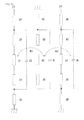
Classifications
-
- H—ELECTRICITY
- H03—ELECTRONIC CIRCUITRY
- H03H—IMPEDANCE NETWORKS, e.g. RESONANT CIRCUITS; RESONATORS
- H03H7/00—Multiple-port networks comprising only passive electrical elements as network components
- H03H7/01—Frequency selective two-port networks
- H03H7/0115—Frequency selective two-port networks comprising only inductors and capacitors
-
- H—ELECTRICITY
- H03—ELECTRONIC CIRCUITRY
- H03H—IMPEDANCE NETWORKS, e.g. RESONANT CIRCUITS; RESONATORS
- H03H5/00—One-port networks comprising only passive electrical elements as network components
- H03H5/02—One-port networks comprising only passive electrical elements as network components without voltage- or current-dependent elements
-
- H—ELECTRICITY
- H03—ELECTRONIC CIRCUITRY
- H03H—IMPEDANCE NETWORKS, e.g. RESONANT CIRCUITS; RESONATORS
- H03H7/00—Multiple-port networks comprising only passive electrical elements as network components
- H03H7/01—Frequency selective two-port networks
- H03H7/09—Filters comprising mutual inductance
-
- H—ELECTRICITY
- H03—ELECTRONIC CIRCUITRY
- H03H—IMPEDANCE NETWORKS, e.g. RESONANT CIRCUITS; RESONATORS
- H03H7/00—Multiple-port networks comprising only passive electrical elements as network components
- H03H7/01—Frequency selective two-port networks
- H03H7/17—Structural details of sub-circuits of frequency selective networks
- H03H7/1741—Comprising typical LC combinations, irrespective of presence and location of additional resistors
- H03H7/1783—Combined LC in series path
-
- H—ELECTRICITY
- H03—ELECTRONIC CIRCUITRY
- H03H—IMPEDANCE NETWORKS, e.g. RESONANT CIRCUITS; RESONATORS
- H03H1/00—Constructional details of impedance networks whose electrical mode of operation is not specified or applicable to more than one type of network
- H03H2001/0021—Constructional details
- H03H2001/0085—Multilayer, e.g. LTCC, HTCC, green sheets
Definitions
- the present invention relates to a multilayer resonator and a multilayer filter, each including a resonance circuit in a multilayer body as a laminate of a plurality of dielectric layers.
- a multilayer filter having a plurality of LC resonance circuits in a multilayer body as a laminate of a plurality of dielectric layers is used as a high-frequency filter.
- the LC resonance circuit may include a capacitor formed of opposing internal electrodes and an inductor formed of a via (for example, see Patent Document 1).
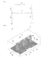
- Fig. 1 illustrates a known multilayer filter.
- Fig. 1(A) is a perspective view of the filter and Fig. 1(B) is a sectional view of the filter.
- a laminate of six layers of insulating sheets 162A-162E is arranged as the multilayer filter 161.
- Vias 163A-163C are arranged in the insulating sheet 162A.
- Vias 164A-164C are arranged in the insulating sheet 162B.
- Vias 165A-165C, and coupling capacitors 166A and 166B are arranged in the insulating sheet 162C.
- Capacitor electrodes 167A-167C are arranged in the insulating sheet [162D] 162E .
- a capacitor electrode 168 is arranged on the insulating sheet 162D, A ground electrode 169C extending from the front surface (not shown) of the multilayer filter 161 to the rear surface (not shown) of the multilayer filter 161 via the top surface is aslso arranged.
- An input-output terminal 169A is arranged on the left end face of the multilayer filter 161 and an input-output terminal 169B is arranged on the right end face of the multilayer filter 161.
- capacitor electrodes 167A and 167C are connected to the input-output terminals 169A and 169B and form resonance circuits at input-output stages.
- routing lines for connecting the capacitor electrodes 167A and 167C to the input-output terminals 169A and 169B are needed.
- the routing lines function as open stubs, and impart a parasitic inductive component to the LC resonator. For this reason, the multilayer filter 161 has an unwanted spurious component in frequency characteristics thereof, and is degraded in attenuation characteristics.
- the ground electrode 169C When the ground electrode 169C is formed on the outer surface of the multilayer filter 161 by plating or other means, loss in the vias 163A-163C increases due to corrosion of the vias 163A-163C. There is a risk that the frequency characteristics of the multilayer filter 161 are degraded. During use, the vias 163A-163C are influenced by an external magnetic field of the multilayer filter 161, There is also a risk that the frequency characteristics of the multilayer filter 161 are degraded.
- a multilayer resonator of the present invention includes first and second capacitor internal electrodes, an inductor internal electrode, a first inductor via electrode, a second inductor via electrode, a first mounting surface connection via electrode, and a second mounting surface connection via electrode.
- the first capacitor internal electrode is mounted to the side of the mounting surface with respect to the second capacitor internal electrode, and is formed so that the first capacitor internal electrode does not overlap a second mounting surface electrode in a see-through plan view taken from one of the main surfaces of the multilayer body.
- a multilayer filter includes a plurality of mutually coupled resonance circuits within a multilayer body.
- the resonance circuit of each of input-output stages includes first and second capacitor internal electrodes, an inductor internal electrode, a first inductor via electrode, a second inductor via electrode, a first mounting surface connection via electrode, and a second mounting surface connection via electrode.
- the first capacitor internal electrode is mounted to the side of the mounting surface with respect to the second capacitor internal electrode, and is formed so that the first capacitor internal electrode does not overlap the second mounting surface electrode in a see-through plan view taken from one of the main surfaces of the multilayer body.
- the first and second capacitor internal electrodes are formed on different dielectric layers in the multilayer body.
- the multilayer body is produced by laminating a plurality of dielectric layers.
- the inductor internal electrode is formed on a dielectric layer different from the dielectric layers of first and second capacitor internal electrodes.
- the first inductor via electrode is electrically connected to the inductor internal electrode and the first capacitor internal electrode.
- the second inductor via electrode is electrically connected to the inductor internal electrode and the second capacitor internal electrode.
- the first mounting surface connection via electrode is electrically connected to the first capacitor internal electrode and a first mounting surface electrode.
- the first mounting surface electrode is formed on the mounting surface of the multilayer body, and serves as one of a ground electrode and an input-output electrode.
- the second mounting surface connection via electrode is electrically connected to the second capacitor internal electrode and a second mounting surface electrode.
- the second mounting surface electrode is formed on the mounting surface of the multilayer body and serves as one of the ground electrode and the input-output electrode.
- the first and second capacitor internal electrodes form a capacitor.
- the inductor internal electrode, the first inductor via electrode and the second inductor via electrode form an inductor.
- the capacitor and the inductor are connected in parallel with each other between the ground terminal and the input-output terminals, and form an LC parallel resonance circuit.
- the mounting surface connection via electrode has a length equal to the thickness of several dielectric layers. Since the length of the via electrode is stable, an inductive component of the LC parallel resonance circuit is also stable.
- the capacitor internal electrode arranged to the side of the mounting surface is formed so that the capacitor internal electrode does not overlap the mounting surface connected to the other capacitor internal electrode if seen through in plan view. Almost no capacitance is thus generated between the capacitor internal electrode and the mounting surface electrode. The capacitance between these electrodes is unwanted in the design point of view of a resonator and a filter. Since such a capacitance is not generated, a capacitive component of the LC parallel resonance circuit becomes stable.
- the inductor Since the inductor is kept within the dielectric layers and is not exposed outside from an outer surface, degradation is not caused during manufacture.
- the inductive component of the resonance circuit becomes stable. Furthermore, the effect of an external magnetic field is controlled during use.
- the first inductor via electrode and the first mounting surface connection via electrode may be co-axially formed.
- the second inductor via electrode and the second mounting surface connection via electrode may be co-axially formed.
- the second capacitor internal electrode may be so formed that the second capacitor internal electrode overlaps the first mounting surface electrode if viewed in a see-through plan view taken from one of the main surfaces of the multilayer body. Since the first capacitor internal electrode is arranged between the second capacitor internal electrode and the first mounting surface electrode, no unwanted capacitance is generated if these electrodes overlap each other.
- the first capacitor internal electrode may be formed on a dielectric layer on the mounting surface. With this arrangement, the length of the via electrode connecting the first capacitor internal electrode to the mounting surface electrode can be controlled, and a parasitic inductive component can be decreased.
- a resonance circuit at an intermediate stage coupled with at least one of the resonance circuits at the input-output stages may be included.
- the resonator at the intermediate stage may include the first and second capacitor internal electrodes, the inductor internal electrode, the first inductor via electrode, the second inductor via electrode, and a mounting surface connection via electrode connected between one of the first and second capacitor internal electrodes and the ground electrode.
- the resonance circuit at the intermediate stage is formed within the multilayer body only. Variations in frequency characteristics due to a deviation of the mounting position are advantageously controlled.
- the mounting surface connection via electrode may be directly electrically connected to the ground electrode.
- no ground electrode is provided within the multilayer body, and the via electrode is directly connected to the ground electrode arranged external to the multilayer body.
- a parasitic inductance otherwise generated in an interlayer ground electrode is thus controlled and design accuracy of the inductor is increased.
- the ground electrode of the resonance circuit at the intermediate stage may be arranged between the input-output electrodes on the mounting surface. With this arrangement, isolation of the input-output electrodes is advantageously increased.
- Each of the resonance circuits may be arranged in perpendicular to the lamination direction of the dielectric layers.
- loops, each formed of the inductor internal electrode, the first inductor via electrode, and the second inductor via electrode in each of the resonance circuits overlap each other if viewed from the direction of the arrangement of the resonance circuits.
- magnetic coupling between the resonance circuits is increased.
- the frequency characteristics are advantageously widened in frequency.
- At least one of the inductor internal electrodes of the resonance circuits may have an electrode width different from the electrode widths of the remaining inductor internal electrodes.
- the inductive component of the inductor in each resonance circuit changes depending on the width of the electrode.
- the inductive component is finely adjusted by varying the electrode width.
- At least one of the inductor internal electrodes of the resonance circuits may be formed on a dielectric layer different from the dielectric layers having the remaining inductor internal electrodes thereon.
- the mounting surface connection via electrode connects the mounting surface electrode to the capacitor internal electrode, and the capacitor internal electrode arranged to the side of the mounting surface is formed so that the capacitor internal electrode does not overlap the mounting surface electrode connected to the other capacitor internal electrode in a see-through plan view.
- the capacitive component and the inductive component of the LC parallel resonance circuit are thus stabilized.
- the frequency characteristics of the resonator and filter are prevented from being degraded.
- a multilayer resonator of a first embodiment of the present invention is described below.
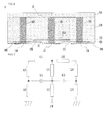
- Fig. 2 is a see-through perspective view of the resonator
- Fig. 3 is a sectional view of the resonator.
- the multilayer resonator 1 is constructed of an LGA (Land Grid Array) package, and includes an input-output electrode 3 and a ground electrode 4 on a mounting surface of a multilayer body 2.
- the surfaces of the multilayer body 2 other than the mounting surface thereof are covered with an unshown metal layer.
- the ground electrode 4 corresponds to a first mounting surface electrode
- the input-output electrode 3 corresponds to a second mounting surface electrode.
- the input-output electrode 3 and the ground electrode 4 are produced by one of means including an application and firing process, a sputtering process, and a vapor deposition process. For this reason, during the mounting of the multilayer resonator 1 to a mother board, a soldering operation on the side face of the multilayer body 2 is eliminated and a soldering area is not required on the mother board.
- the multilayer resonator 1 thus permits a high-density mounting.
- the multilayer body 2 is produced by laminating a plurality of dielectric layers in a vertical direction of Fig. 3 as a lamination direction and firing the laminate.
- the plurality of dielectric layers 2A-2D are thus produced.
- the dielectric layers 2A-2D are rectangular plates, and made of a low temperature co-fired ceramic (LTCC) having a specific dielectric constant ⁇ r 53.5, LTCC contains glass and at least one material selected from the group consisting of titanium oxide, barium oxide, and aluminum oxide.
- LTCC low temperature co-fired ceramic
- the multilayer body 2 contains therewithin an inductor internal electrode 5, inductor via electrodes 6A and 68, capacitor internal electrodes 7A and 7B, an input-output via electrode 8, and a ground via electrode 9.
- the capacitor internal electrode 7B corresponds to a first capacitor internal electrode
- the capacitor internal electrode 7A corresponds to a second capacitor internal electrode.
- the ground via electrode 9 corresponds to a first mounting surface connection via electrode
- the input-output via electrode 8 corresponds to a second mounting surface connection via electrode.
- the internal electrodes 5, 7A, and 7B are made of Ag, Pd, Cu, Au, Ag-Pd, or the like, and is produced using means such as printing.
- the via electrodes 6A, 68, 8, and 9 are produced as via holes arranged in each dielectric layer or as a plurality of noming via holes. Each via hole is produced by filling holes arranged beforehand on the dielectric sheet with an electrically conductive paste of Ag, Pd, Cu, Au, Ag-Pd, or the like.
- the inductor internal electrode 5 is a line electrode formed on the dielectric layer 2B.
- the inductor via electrode 6A is a via hole arranged in the dielectric layer 2B.
- the inductor via electrode 6A is arranged below the left end portion of the inductor internal electrode 5 as illustrated in Fig. 3 and connects the inductor internal electrode 5 to the capacitor internal electrode 7A.
- the inductor via electrode 6B is an electrode connecting a via hole arranged in the dielectric layer 2B to a via hole arranged in the dielectric layer 2C.
- the inductor via electrode 6B is arranged below the right end portion of the inductor internal electrode 5 as illustrated in Fig. 3 and connects the inductor internal electrode 5 to the capacitor internal electrode 7B.
- the capacitor internal electrode 7A is a rectangular electrode formed on the dielectric layer 2C.
- the capacitor internal electrode 7B is a rectangular electrode formed on the dielectric layer 2D.
- the right portion of the capacitor internal electrode 7A illustrated in Fig. 3 is opposed to the left portion of the capacitor internal electrode 7B illustrated in Fig. 3 with the dielectric layer 2C interposed therebetween.
- the input-output via electrode 8 is an electrode that connects a via hole arranged in the dielectric layer 2C to a via hole arranged in the dielectric layer 2D.
- the input-output via electrode 8 is arranged to be co-axial with the inductor via electrode 6A and connects the capacitor internal electrode 7A to the input-output electrode 3.
- the ground via electrode 9 is a via hole arranged in the dielectric layer 2D.
- the ground via electrode 9 is arranged to be co-axial with the inductor via electrode 6B and connects the capacitor internal electrode 78 to the ground electrode 4. Opposed electrode areas of the capacitor internal electrode 7A and the capacitor internal electrode 7B are set in order to generate a required capacitance.
- each electrode forms an LC parallel resonance circuit.
- the input-output electrode 3 and the capacitor internal electrode 7B are arranged herein so that these elements do not overlap each other in a see-through plan view. Since the input-output electrode 3 and the ground electrode 4 are typically produced using the thick-film formation method such as screen printing, large dimensional variations result. There are cases when the input-output electrode 3 and the ground electrode 4 are reduced in size as a result of partial grinding during barrel-polishing of the multilayer body. If the input-output electrode 3 and the ground electrode 4 are arranged to overlap each other, a capacitance unwanted in the design point of view is generated between the input-output electrode 3 and the capacitor internal electrode 7B. Moreover, there is a possibility that variations in electrode shape lead to variations in capacitance value.
- the input-output electrode 3 and the capacitor internal electrode 7B are arranged not to overlap each other in a see-through plan view, the generation of the unwanted capacitance is prevented. Even if there are variations in shape of the input-output electrode 3 and the ground electrode 4, a capacitive component of the LC parallel resonance circuit is stabilized, and variations in resonator characteristics are controlled.
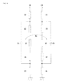
- Fig. 4 is an equivalent circuit diagram of the multilayer resonator 1.
- the capacitor internal electrode 7A and the capacitor internal electrode 78 form a capacitance C1.
- the inductor via electrodes 6A and 6B and the inductor internal electrode 5 are arranged in a loop configuration.
- the inductor internal electrode 5 forms an inductance L1
- the inductor via electrode 6A forms an inductance L2
- the inductor via electrode 6B forms an inductance L3.
- the capacitor and the inductors form the LC parallel resonance circuit and are connected in parallel between the input-output electrode 3 and the ground electrode 4 via the input-output via electrode 8 and the ground via electrode 9.
- the input-output electrode 3 is thus connected to the LC parallel resonance circuit.
- the input-output via electrode 8 forms an inductance L4 and the ground via electrode 9 forms an inductance L5.
- the input-ouput electrode 3 and the ground electrode 4 are connected to the LC parallel resonance circuit via the via holes.
- This arrangement provides a higher connection reliability than the related art in which an extension line is used. Since the multilayer resonator 1 is constructed of the LGA package, a high contact reliability of electrodes to a mother board is achieved in the mounting of the multilayer resonator 1 to the mother board. During the mounting of the multilayer resonator 1 to the mother board, a soldering operation on the side face of the multilayer body 2 is eliminated and a soldering area is not required on the mother board. The multilayer resonator 1 thus permits a high-density mounting. Since no soldering operation is required during the mounting, a reduction of the number of process steps is expected.
- the inductances L4 and L5 formed by the input-output via electrode 8 and the ground via electrode 9 function as a parasitic inductive component, imparting an unwanted spurious component to the LC parallel resonance circuit.
- the length of each of the input-output via electrode 8 and the length of the ground via electrode 9 are respectively the thickness of the dielectric layer 2D and the sum of thicknesses of the dielectric layer 2C and the dielectric layer 2D.
- the open stub length of each of the electrodes degrading attenuation characteristics is short. The unwanted spurious component affecting the attenuation characteristics of the multilayer resonator 1 is still limited.
- the inductor via electrodes 6A and 6B and the inductor internal electrode 5 are formed within the multilayer body 2, electrode corrosion is not caused during a plating process of the muitilayer body 2. For this reason, no increase takes place in filter loss. Since the inductor via electrodes 6A and 6B and the inductor internal electrode 5 are formed in a loop configuration within the multilayer body 2, the multilayer body 2 is less susceptible to an external magnetic field, and variations in the characteristics are controlled. This arrangement offers excellent shielding property and excellent control property on unwanted radiations.
- the multilayer resonator 1 having electrical characteristics stable to high-frequency regions is thus provided.
- the multilayer resonator 1 is herein constructed so that a loop plane of the inductors is perpendicular to the short-side direction of the multilayer body 2.
- the multilayer resonator 1 is thus miniaturized, Alternatively, the loop plane of the inductors may be perpendicular to the long-side direction of the multilayer body 2.
- the capacitor internal electrode 7B is arranged on the top surface of the dielectric layer 2D which is adjacent to the mounting surface, and the capacitor internal electrode 7A is arranged on the top surface of the dielectric layer 2C which is adjacent to the dielectric layer 2D.
- the capacitor internal electrode 7B and the capacitor internal electrode 7A may be reversed in the vertical positions thereof.
- the capacitor internal electrode 7A is arranged not to overlap the ground electrode 4 if seen through from above. Alternatively, the capacitor internal electrode 7A may overlap the ground electrode 4. Since the capacitor internal electrode 78 is arranged between the capacitor internal electrode 7A and the ground electrode 4, an unwanted capacitance is not generated if the two electrodes overlap each other.
- the multilalyer resonator of the second embodiment is different from the multilayer resonator 1 of the first embodiment in that two resonance circuits are arranged in the multilayer body and that two ground electrodes are arranged on the mounting surface.
- Fig. 5 is a see-through perspective view of the resonator
- Fig. 6 is a sectional view of the resonator.
- the multilayer resonator 11 includes an input-output electrode 13 and ground electrodes 14A and 14B on the mounting surface of the multilayer body 12.
- the multilayer body 12 includes a plurality of dielectric layers 12A-12D. Arranged within the multilayer body 12 are an inductor internal electrode 15, inductor via electrodes 16A-16C, capacitor internal electrodes 17A-17C, an input-output via electrode 18, and ground via electrodes 19A and 19B.
- the inductor internal electrode 15 is a line electrode formed on the dielectric layer 12B.
- the inductor via electrode 16A is a via hole arranged in the dielectric layer 12B.
- the inductor via electrode 16A is arranged below the center portion of the inductor internal electrode 15 and connects the inductor internal electrode 15 to the capacitor internal electrode 17A.
- Each of the inductor via electrodes 16B and 16C is formed by connecting a via hole in the dielectric layer 12B to a via hole in the dielectric layer 12C.
- the inductor via electrodes 16B and 16C are arranged below the two end portions of the inductor internal electrode 15 and connects the inductor internal electrode 15 to the capacitor internal electrodes 17B and 17C.
- the capacitor internal electrode 17A is a rectangular electrode formed on the dielectric layer 12C.
- the capacitor internal electrodes 17B and 17C are rectangular electrodes formed on the dielectric layer 12D.
- the two end portions of the capacitor internal electrode 17A are respectively opposed to a portion of the capacitor internal electrode 17B and a portion of the capacitor internal electrode 17C with the dielectric layer 12C interposed therebetween.
- Said portion of the capacitor internal electrode 17B and the portion of the capacitor internal electrode 17C are portions close to the center of the multilayer body 2.
- the input-output via electrode 18 is formed by connecting a via hole in the dielectric layer 12C to a via hole in the dielectric layer 12D.
- the input-output via electrode 18 is arranged to be co-axial with the inductor via electrode 16A and connects the capacitor internal electrode 17A to the input-output electrode 13.
- the ground via electrodes 19A and 19B are via holes arranged in the dielectric layer 12D.
- the ground via electrodes 19A and 19B are arranged to be co-axial with the inductor via electrodes 16B and 16C, respectively, and connect the capacitor internal electrodes 17B and 17C to the ground electrodes 14A and 14B, respectively.
- the multilayer resonator 11 thus constructed has a circuit arrangement of two LC parallel resonance circuits that are connected in parallel.
- the input-output electrode 13 and the capacitor internal electrodes 17B and 17C are arranged so that no overlapping portion is caused if seen through from above. In this way, the generation of the above-described unwanted capacitance is prevented. Even if the input-output electrode 13 is changed in shape, the capacitive component of the LC parallel resonance circuit is stabilized, and variations in the resonance characteristics are controlled.
- Fig. 7 is an equivalent circuit diagram of the multilayer resonator 11.
- the capacitor internal electrode 17A and the capacitor internal electrode 17B form a capacitance C11.
- the inductor via electrodes 16B and 16C and the inductor internal electrode 15 are arranged in a loop configuration. Part of the inductor internal electrode 15 forms an inductance L11, the inductor via electrode 16A forms an inductance L14, and the inductor via electrode 16B forms an inductance L13.
- the capacitor and the inductors form a first LC parallel resonance circuit, and are connected in parallel between the input-output electrode 13 and the ground electrode 14A via the input-output via electrode 18 and the ground via electrode 19A.
- the capacitor internal electrode 17A and the capacitor internal electrode 17C form a capacitance C12.
- the inductor via electrodes 16A and 16C and the inductor internal electrode 15 are arranged in a loop configuration. Part of the inductor internal electrode 15 forms the inductance L12, the inductor via electrode 16A forms the inductance L14, and the inductor via electrode 16C forms an inductance L15.
- the capacitor and the inductors form a second LC parallel resonance circuit, and are connected in parallel between the input-output electrode 13 and the ground electrode 14B via the input-output via electrode 18 and the ground via electrode 19B.
- the multilayer resonator 11 functions as a resonance circuit that includes the two LC parallel resonance circuits connected in parallel.
- the input-output via electrode 18 forms an inductance L17
- the ground via electrode 19A forms an inductance L16
- the ground via electrode 19B forms an inductance L18.
- these inductances function as parasitic inductive components, the length of each electrode is short, and the open stub length of each of these electrodes degrading attenuation characteristics is short. The unwanted spurious effect affecting the attenuation characteristics of the multilayer resonator 11 is still limited.
- the present invention can be embodied regardless of the structure of the resonance circuit arranged within the multilayer body, and the effect of the unwanted spurious component to the attenuation characteristics of the multilayer resonator is controlled. Since the inductor via electrodes and the inductor internal electrode are arranged in a loop configuration within the multilayer body, electrode corrosion is prevented during the plating process, and the influence of an external magnetic field is controlled. Variations in the characteristics are controlled.
- a multilayer filter of a third embodiment of the present invention is described.
- the multilayer filter of the third embodiment is different from the structure of the first embodiment in that two resonance circuits are arranged within the multilayer body.
- Each resonance circuit has the same circuit arrangement as the resonance circuit of the first embodiment.
- Fig. 8 is a see-through perspective view of the filter.
- the multilayer filter 21 includes input-output electrodes 23 and 33 and ground electrodes 24 and 34 on the mounting surface of a multilayer body 22.
- Arranged within the multilayer body 22 are inductor internal electrodes 25 and 35, inductor via electrodes 26A, 26B, 36A, and 36B, capacitor internal electrodes 27A, 27B, 37A, and 37B, input-output via electrodes 28 and 38, and ground via electrodes 29 and 39.
- a first LC parallel resonance circuit includes the input-output electrode 23, the ground electrode 24, the inductor internal electrode 25, the inductor via electrodes 26A and 26B, the capacitor internal electrodes 27A and 27B, the input-output via electrode 28, and the ground via electrode 29.
- a second LC parallel resonance circuit includes the input-output electrode 33, the ground electrode 34, the inductor internal electrode 35, the inductor via electrodes 36A and 36B, the capacitor internal electrodes 37A and 37B, the input-output via electrode 38, and the ground via electrode 39.
- the first LC parallel resonance circuit and the second LC parallel resonance circuit are arranged within the multilayer body 22 so that the loop planes of the circuits face each other.
- the loops overlap each other if viewed in the direction of the arrangement.
- a magnetic field flux passing through the loops are shared by the first LC parallel resonance circuit and the second LC parallel resonance circuit, and the two LC resonance circuits are thus magnetically coupled.
- the input-output electrode 23 and the capacitor internal electrode 27B are arranged not to overlap each other if seen through from above.
- the input-output electrode 33 and the capacitor internal electrode 37B are arranged not to overlap each other if seen through from above. This arrangement controls the generation of an unwanted capacitance. Even if the input-output electrodes 23 and 33 are changed in shape, the capacitive component of the LC parallel resonance circuits remain stable, and variations in the resonator characteristics are controlled.
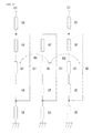
- Fig. 9 is an equivalent circuit diagram of the multilayer filter 21.
- the capacitor internal electrode 27A and the capacitor internal electrode 27B form a capacitance C21.
- the inductor via electrodes 26A and 26B and the inductor internal electrode 25 are arranged in a loop configuration.
- the inductor internal electrode 25 forms an inductance L21
- the inductor via electrode 26A forms an inductance L22
- the inductor via electrode 26B forms an inductance L23.
- the capacitor and the inductors form the first LC parallel resonance circuit and are connected in parallel between the input-output electrode 23 and the ground electrode 24 via the input-output via electrode 28 and the ground via electrode 29.
- the capacitor internal electrode 37A and the capacitor internal electrode 37B form a capacitance C31.
- the inductor via electrodes 36A and 36B and the inductor internal electrode 35 are arranged in a loop configuration.
- the inductor internal electrode 35 forms an inductance L31
- the inductor via electrode 36A forms an inductance L32
- the inductor via electrode 36B forms an inductance L33.
- the capacitor and the inductors form the second LC parallel resonance circuit and are connected in parallel between the input-output electrode 33 and the ground electrode 34 via the input-output via electrode 38 and the ground via electrode 39.
- the input-output electrode 23 is connected to the first LC parallel resonance circuit and the input-output electrode 33 is connected to the second LC parallel resonance circuit, and the LC parallel resonance circuits become respectively resonance circuits at the input-output stages.
- the overlapping of the loops of the LC parallel resonance circuits generate a magnetic coupling M21.
- the multilayer filter 21 with the above-described circuit arrangement functions as a bandpass filter composed of the two-stage LC parallel resonance circuits.
- the input-output via electrode 28 forms an inductance L24
- the input-output via electrode 38 forms an inductance L34
- the ground via electrode 29 forms an inductance L25
- the ground via electrode 39 forms an inductance L35.
- the multilayer filter 21 of the present invention can be embodied regardless of the structure of the resonance circuits arranged within the multilayer body, and the effect of the unwanted spurious component to the attenuation characteristics of the multilayer resonator is controlled. Since the inductor via electrodes and the inductor internal electrodes are arranged in a loop configuration within the multilayer body, electrode corrosion is prevented during the plating process, and the influence of an external magnetic field is controlled. Variations in the characteristics are controlled.
- a multilayer filter of a fourth embodiment of the present invention is described.
- the multilayer filter of the fourth embodiment is different from the structure of the third embodiment in that a resonance circuit at an intermediate state is arranged within the multilayer body.
- Fig. 10 is a see-through perspective view of the filter.
- the multilayer filter 41 includes input-output electrodes 43 and 63, and ground electrodes 44, 54, and 64 on the mounting surface of a multilayer body 42.
- Arranged within the multilayer body 42 are inductor internal electrodes 45, 55, and 65, inductor via electrodes 46A, 46B, 56A, 56B, 66A and 66B, capacitor internal electrodes 47A, 47B, 57A, 57B, 67A, and 67B, input-output via electrodes 48 and 68, and ground via electrodes 49, 59, and 69.
- a LC parallel resonance circuit at a first input-output stage includes the input-output electrode 43, the ground electrode 44, the inductor internal electrode 45, the inductor via electrodes 46A and 46B, the input-output via electrode 48, and the ground via electrode 49.
- An LC parallel resonance circuit at an intermediate stage includes the ground electrode 54, the inductor internal electrode 55, the inductor via electrodes 56A and 56B, the capacitor internal electrodes 57A and 57B, and the ground via electrode 59.
- the LC parallel resonance circuit at the intermediate stage has neither input-output via electrode nor input-output electrode.
- a second LC parallel resonance circuit at an input-output stage includes the input-output electrode 63, the ground electrode 64, the inductor internal electrode 65, the inductor via electrodes 66A and 66B, the capacitor internal electrodes 67A and 67B, the input-output via electrode 68, and the ground via electrode 69.
- the three LC parallel resonance circuits are arranged within the multilayer body 42 so that the loop planes thereof are opposed to each other.
- the loop planes overlap each other if viewed in the arrangement direction.
- a magnetic field flux passing through the loops are shared by the three LC parallel resonance circuits, and two adjacent LC resonance circuits are thus magnetically coupled.
- the input-output electrode 43 and the capacitor internal electrode 47B are arranged not to overlap each other if seen through from above.
- the input-output electrode 63 and the capacitor internal electrode 67B are arranged not to overlap each if seen through from above. This arrangement controls the generation of an unwanted capacitance. Even if the input-output electrodes 43 and 63 are changed in shape, the capacitive component of the LC parallel resonance circuits remain stable, and variations in the resonator characteristics are controlled.
- Fig. 11 is an equivalent circuit diagram of the multilayer fitter 41.
- the capacitor internal electrode 47A and the capacitor internal electrode 47B form a capacitance C41.
- the inductor via electrodes 46A and 46B and the inductor internal electrode 45 are arranged in a loop configuration.
- the inductor internal electrode 45 forms an inductance L41
- the inductor via electrode 46A forms an inductance L42
- the inductor via electrode 46B forms an inductance L43.
- the capacitor and the inductors forms LC parallel resonance circuit at a first input-output stage and are connected in parallel between the input-output electrode 43 and the ground electrode 44 via the input-output via electrode 48 and the ground via electrode 49.
- the capacitor internal electrode 57A and the capacitor internal electrode 57B form a capacitance C51.
- the inductor via electrodes 56A and 56B and the inductor internal electrode 55 are arranged in a loop configuration.
- the inductor internal electrode 55 forms an inductance L51
- the inductor via electrode 56A forms an inductance L52
- the inductor via electrode 56B forms an inductance L53.
- the capacitor and the inductors form an LC parallel resonance circuit at an intermediate state, and are connected to the ground electrode 54 via the ground via electrode 59.
- the capacitor internal electrode 67A and the capacitor internal electrode 67B form a capacitance C61.
- the inductor via electrodes 66A and 66B and the inductor internal electrode 65 are arranged in a loop configuration.
- the inductor internal electrode 65 forms an inductance L61
- the inductor via electrode 66A forms an inductance L62
- the inductor via electrode 66B forms an inductance L63.
- the capacitor and the inductors form a LC parallel resonance circuit at a second input-output stage and are connected in parallel between the input-output electrode 63 and the ground electrode 64 via the input-output via electrode 68 and the ground via electrode 69.
- the input-output electrode 43 is connected to the LC parallel resonance circuit at the first input-output stage, and the input-output electrode 63 is connected to the LC parallel resonance circuit at the second input-output stage.
- the overlapping of the LC parallel resonance circuits generates magnetic couplings M41 and M42.
- the multilayer filter 41 with the circuit arrangement described above functions as a bandpass filter composed of the three-stage LC parallel resonance circuits.
- the input-output via electrode 48 forms an inductance L44
- the input-output via electrode 68 forms an inductance L64
- the ground via electrode 49 forms an inductance L45
- the ground via electrode 59 forms an inductance L55
- the ground via electrode 69 forms an inductance L65.
- the multilayer filter of the present invention can be embodied regardless of the structure of the resonance circuits arranged within the multilayer body, and the effect of the unwanted spurious component to the attenuation characteristics of the multilayer resonator is controlled. Since the inductor via electrodes and the inductor internal electrodes are arranged in a loop configuration within the multilayer body, electrode corrosion is prevented during the plating process, and the influence of an external magnetic field is controlled. Variations in the characteristics are controlled.
- a multilayer filter of a fifth embodiment of the present invention is described below.
- the multilayer filter of the fifth embodiment is different from the structure of the fourth embodiment in that the resonance circuit at the intermediate stage is reversed in direction.
- Fig. 12 is a see-through perspective view of the filter.
- the multilayer filter 71 includes input-output electrodes 73 and 93 and ground electrodes 74, 84, and 94 on the mounting surface of a multilayer body 72.
- Arranged within the multilayer body 72 are inductor internal electrodes 75, 85, and 95, inductor via electrodes 76A, 76B, 86A, 86B, 96A, and 96B, capacitor internal electrodes 77A, 77B, 87A, 87B, 97A, and 97B, input-output via electrode 78 and 98, and ground via electrodes 79, 89, and 99.
- a LC parallel resonance circuit at a first input-output stage includes the input-output electrode 73, the ground electrode 74, the inductor internal electrode 75, the inductor via electrodes 76A and 76B, the capacitor internal electrodes 77A and 77B, the input-output via electrode 78, and the ground via electrode 79.
- An LC parallel resonance circuit at an intermediate stage includes the ground electrode 84, the inductor internal electrode 85, the inductor via electrodes 86A and 86B, the capacitor internal electrodes 87A and 87B, and the ground via electrode 89.
- the LC parallel resonance circuit at the intermediate stage has neither input-output via electrode nor input-output electrode.
- a LC parallel resonance circuit at a second input-output stage includes the input-output electrode 93, the ground electrode 94, the inductor internal electrode 95, the inductor via electrodes 96A and 96B, the capacitor internal electrodes 97A and 978, the input-output via electrode 98, and the ground via electrode 99.
- the three LC parallel resonance circuits are arranged within the multilayer body 72 so that the loop planes thereof are opposed to each other.
- the loop planes overlap each other if viewed in the arrangement direction.
- the loop of the LC parallel resonance circuit at the intermediate stage is opposite in direction to the loops of the LC parallel resonance circuits at the input-output stages.
- the ground electrode 84 of the resonance circuit at the intermediate stage is arranged between the input-output electrodes 73 and 93. This arrangement improves isolation between the input-output electrodes 73 and 93.
- a magnetic field flux passing through the loops are shared by the three LC parallel resonance circuits, and two adjacent LC resonance circuits are thus magnetically coupled.
- the input-output electrode 73 and the capacitor internal electrode 778 are arranged not to overlap each other if seen through from above.
- the input-output electrode 93 and the capacitor internal electrode 97B are arranged not to overlap each if seen through from above. This arrangement controls the generation of an urwanted capacitance. Even if the input-output electrodes 73 and 93 are changed in shape, the capacitive component of the LC parallel resonance circuits remain stable, and variations in the resonator characteristics are controlled.
- Fig. 13 is an equivalent circuit diagram of the multilayer filter 71.
- the capacitor internalel ectrode 77A and the capacitor internal electrode 77B form a capacitance C71.
- the inductor via electrodes 76A and 768 and the inductor internal electrode 75 are arranged in a loop configuration.
- the inductor internal electrode 75 forms an inductance L71
- the inductor via electrode 76A forms an inductance L72
- the inductor via electrode 76B forms an inductance L73.
- the capacitor and the inductors form the LC parallel resonance circuit at the first input-output stage and are connected in parallel between the input-output electrode 73 and the ground electrode 74 via the input-output via electrode 78 and the ground via electrode 79.
- the capacitor internal electrode 87A and the capacitor internal electrode 87B form a capacitance C81.
- the inductor via electrodes 86A and 86B and the inductor internal electrode 85 are arranged in a loop configuration.
- the inductor internal electrode 85 forms an inductance L81
- the inductor via electrode 86A forms an inductance L82
- the inductor via electrode 86B forms an inductance L83.
- the capacitor and the inductors form the LC parallel resonance circuit at the intermediate state, and are connected to the ground electrode 84 via the ground via electrode 89.
- the capacitor internal electrode 97A and the capacitor internal electrode 97B form a capacitance C91.
- the inductor via electrodes 96A and 96B and the inductor internal electrode 95 are arranged in a loop configuration.
- the inductor internal electrode 95 forms an inductance L91
- the inductor via electrode 96A forms an inductance L92
- the inductor via electrode 968 forms an inductance L93.
- the capacitor and the inductors form the LC parallel resonance circuit at the second input-output stage and are connected in parallel between the input-output electrode 93 and the ground electrode 94 via the input-output via electrode 98 and the ground via electrode 99.
- the input-output electrodes 73 is connected to the LC parallel resonance circuit at the first input-output stage, and the input-output electrode 93 is connected to the LC parallel resonance circuit at the second input-output stage.
- the overlapping of the LC parallel resonance circuits generates magnetic couplings M71 and M72.
- the multilayer filter 71 with the circuit arrangement described above functions as a bandpass filter composed of the three-stage LC parallel resonance circuits.
- the input-output via electrode 78 forms an inductance L74
- the input-output via electrode 98 forms an inductance L94
- the ground via electrode 79 forms an inductance L75
- the ground via electrode 89 forms an inductance [L85] L84
- the ground via electrode 99 forms an inductance L95.
- the multilayer filter of the present invention can be embodied regardless of the structure of the resonance circuits arranged within the multilayer body, and the effect of the unwanted spurious component to the attenuation characteristics of the multilayer resonator is controlled. Since the inductor via electrodes and the inductor internal electrodes are arranged in a loop configuration within the multilayer body, electrode corrosion is prevented during the plating process, and the influence of an external magnetic field is controlled. Variations in the characteristics are controlled
Landscapes
- Engineering & Computer Science (AREA)
- Power Engineering (AREA)
- Filters And Equalizers (AREA)
- Fixed Capacitors And Capacitor Manufacturing Machines (AREA)
- Coils Or Transformers For Communication (AREA)
- Control Of Motors That Do Not Use Commutators (AREA)
Abstract
Description
- The present invention relates to a multilayer resonator and a multilayer filter, each including a resonance circuit in a multilayer body as a laminate of a plurality of dielectric layers.
- A multilayer filter having a plurality of LC resonance circuits in a multilayer body as a laminate of a plurality of dielectric layers is used as a high-frequency filter. The LC resonance circuit may include a capacitor formed of opposing internal electrodes and an inductor formed of a via (for example, see Patent Document 1).
-
Fig. 1 illustrates a known multilayer filter.Fig. 1(A) is a perspective view of the filter andFig. 1(B) is a sectional view of the filter.
A laminate of six layers ofinsulating sheets 162A-162E is arranged as themultilayer filter 161.Vias 163A-163C are arranged in theinsulating sheet 162A.Vias 164A-164C are arranged in theinsulating sheet 162B.Vias 165A-165C, and coupling capacitors 166A and 166B are arranged in theinsulating sheet 162C. Capacitor electrodes 167A-167C are arranged in the insulating sheet [162D] 162E. Acapacitor electrode 168 is arranged on theinsulating sheet 162D, A ground electrode 169C extending from the front surface (not shown) of themultilayer filter 161 to the rear surface (not shown) of themultilayer filter 161 via the top surface is aslso arranged. An input-output terminal 169A is arranged on the left end face of themultilayer filter 161 and an input-output terminal 169B is arranged on the right end face of themultilayer filter 161. - Patent Document 1: Japanese Unexamined Patent Application Publication (Translation of PCT Application) No.
2000-165171 - In the
multilayer filter 161, capacitor electrodes 167A and 167C are connected to the input-output terminals 169A and 169B and form resonance circuits at input-output stages. With this arrangement, routing lines for connecting the capacitor electrodes 167A and 167C to the input-output terminals 169A and 169B are needed. The routing lines function as open stubs, and impart a parasitic inductive component to the LC resonator. For this reason, themultilayer filter 161 has an unwanted spurious component in frequency characteristics thereof, and is degraded in attenuation characteristics. - When the ground electrode 169C is formed on the outer surface of the
multilayer filter 161 by plating or other means, loss in thevias 163A-163C increases due to corrosion of thevias 163A-163C. There is a risk that the frequency characteristics of themultilayer filter 161 are degraded. During use, thevias 163A-163C are influenced by an external magnetic field of themultilayer filter 161, There is also a risk that the frequency characteristics of themultilayer filter 161 are degraded. - It is an object of the present invention to provide a multilayer resonator and a multilayer filter, each controlling frequency characteristics thereof with an inductive component and a capacitive component stabilized in the resonance circuit thereof.
- A multilayer resonator of the present invention includes first and second capacitor internal electrodes, an inductor internal electrode, a first inductor via electrode, a second inductor via electrode, a first mounting surface connection via electrode, and a second mounting surface connection via electrode. The first capacitor internal electrode is mounted to the side of the mounting surface with respect to the second capacitor internal electrode, and is formed so that the first capacitor internal electrode does not overlap a second mounting surface electrode in a see-through plan view taken from one of the main surfaces of the multilayer body.
- A multilayer filter includes a plurality of mutually coupled resonance circuits within a multilayer body. The resonance circuit of each of input-output stages includes first and second capacitor internal electrodes, an inductor internal electrode, a first inductor via electrode, a second inductor via electrode, a first mounting surface connection via electrode, and a second mounting surface connection via electrode. The first capacitor internal electrode is mounted to the side of the mounting surface with respect to the second capacitor internal electrode, and is formed so that the first capacitor internal electrode does not overlap the second mounting surface electrode in a see-through plan view taken from one of the main surfaces of the multilayer body.
- The first and second capacitor internal electrodes are formed on different dielectric layers in the multilayer body. The multilayer body is produced by laminating a plurality of dielectric layers. The inductor internal electrode is formed on a dielectric layer different from the dielectric layers of first and second capacitor internal electrodes. The first inductor via electrode is electrically connected to the inductor internal electrode and the first capacitor internal electrode. The second inductor via electrode is electrically connected to the inductor internal electrode and the second capacitor internal electrode. The first mounting surface connection via electrode is electrically connected to the first capacitor internal electrode and a first mounting surface electrode. The first mounting surface electrode is formed on the mounting surface of the multilayer body, and serves as one of a ground electrode and an input-output electrode. The second mounting surface connection via electrode is electrically connected to the second capacitor internal electrode and a second mounting surface electrode. The second mounting surface electrode is formed on the mounting surface of the multilayer body and serves as one of the ground electrode and the input-output electrode.
- The first and second capacitor internal electrodes form a capacitor. The inductor internal electrode, the first inductor via electrode and the second inductor via electrode form an inductor. The capacitor and the inductor are connected in parallel with each other between the ground terminal and the input-output terminals, and form an LC parallel resonance circuit.
- With the above-described arrangement, the mounting surface connection via electrode has a length equal to the thickness of several dielectric layers. Since the length of the via electrode is stable, an inductive component of the LC parallel resonance circuit is also stable.
- The capacitor internal electrode arranged to the side of the mounting surface is formed so that the capacitor internal electrode does not overlap the mounting surface connected to the other capacitor internal electrode if seen through in plan view. Almost no capacitance is thus generated between the capacitor internal electrode and the mounting surface electrode. The capacitance between these electrodes is unwanted in the design point of view of a resonator and a filter. Since such a capacitance is not generated, a capacitive component of the LC parallel resonance circuit becomes stable.
- Since the inductor is kept within the dielectric layers and is not exposed outside from an outer surface, degradation is not caused during manufacture. The inductive component of the resonance circuit becomes stable. Furthermore, the effect of an external magnetic field is controlled during use.
- The first inductor via electrode and the first mounting surface connection via electrode may be co-axially formed. The second inductor via electrode and the second mounting surface connection via electrode may be co-axially formed.
- The second capacitor internal electrode may be so formed that the second capacitor internal electrode overlaps the first mounting surface electrode if viewed in a see-through plan view taken from one of the main surfaces of the multilayer body. Since the first capacitor internal electrode is arranged between the second capacitor internal electrode and the first mounting surface electrode, no unwanted capacitance is generated if these electrodes overlap each other.
- The first capacitor internal electrode may be formed on a dielectric layer on the mounting surface. With this arrangement, the length of the via electrode connecting the first capacitor internal electrode to the mounting surface electrode can be controlled, and a parasitic inductive component can be decreased.
- A resonance circuit at an intermediate stage coupled with at least one of the resonance circuits at the input-output stages may be included. In such a case, the resonator at the intermediate stage may include the first and second capacitor internal electrodes, the inductor internal electrode, the first inductor via electrode, the second inductor via electrode, and a mounting surface connection via electrode connected between one of the first and second capacitor internal electrodes and the ground electrode. The resonance circuit at the intermediate stage is formed within the multilayer body only. Variations in frequency characteristics due to a deviation of the mounting position are advantageously controlled.
- The mounting surface connection via electrode may be directly electrically connected to the ground electrode. In this case, no ground electrode is provided within the multilayer body, and the via electrode is directly connected to the ground electrode arranged external to the multilayer body. A parasitic inductance otherwise generated in an interlayer ground electrode is thus controlled and design accuracy of the inductor is increased.
- The ground electrode of the resonance circuit at the intermediate stage may be arranged between the input-output electrodes on the mounting surface. With this arrangement, isolation of the input-output electrodes is advantageously increased.
- Each of the resonance circuits may be arranged in perpendicular to the lamination direction of the dielectric layers. In this case, loops, each formed of the inductor internal electrode, the first inductor via electrode, and the second inductor via electrode in each of the resonance circuits, overlap each other if viewed from the direction of the arrangement of the resonance circuits. With this arrangement, magnetic coupling between the resonance circuits is increased. The frequency characteristics are advantageously widened in frequency.
- At least one of the inductor internal electrodes of the resonance circuits may have an electrode width different from the electrode widths of the remaining inductor internal electrodes. The inductive component of the inductor in each resonance circuit changes depending on the width of the electrode. The inductive component is finely adjusted by varying the electrode width.
- At least one of the inductor internal electrodes of the resonance circuits may be formed on a dielectric layer different from the dielectric layers having the remaining inductor internal electrodes thereon. With this arrangement, the design flexibility of the inductor internal electrode is increased. Since the inductive component of the inductor in each resonance circuit varies depending on the electrode width of the inductor internal electrode, the inductive component can be finely adjusted by setting the electrode length to any value. Since the design flexibility of the inductor internal electrode is increased, the design flexibility of the LC parallel resonance circuit is also increased.
- In accordance with the present invention, the mounting surface connection via electrode connects the mounting surface electrode to the capacitor internal electrode, and the capacitor internal electrode arranged to the side of the mounting surface is formed so that the capacitor internal electrode does not overlap the mounting surface electrode connected to the other capacitor internal electrode in a see-through plan view. The capacitive component and the inductive component of the LC parallel resonance circuit are thus stabilized. The frequency characteristics of the resonator and filter are prevented from being degraded.
-
- [
Fig. 1] Fig. 1 illustrates a structure of a known multilayer filter. - [
Fig. 2] Fig. 2 is a see-through perspective view of a multilayer resonator of a first embodiment of the present invention. - [
Fig. 3] Fig. 3 is a sectional view of the resonator. - [
Fig. 4] Fig. 4 is an equivalent circuit diagram of the resonator. - [
Fig. 5] Fig. 5 is a see-through perspective view of a multilayer resonator of a second embodiment of the present invention. - [
Fig. 6] Fig. 6 is a sectional view of the resonator. - [
Fig. 7] Fig. 7 is an equivalent circuit diagram of the resonator. - [
Fig. 8] Fig. 8 is a see-through perspective view of a multilayer filter of a third embodiment of the present invention. - [
Fig. 9] Fig. 9 is an equivalent circuit diagram of the filter. - [
Fig. 10] Fig. 10 is a see-through perspective view of a multilayer filter of a fourth embodiment of the present invention. - [
Fig. 11] Fig. 11 is an equivalent circuit diagram of the filter. - [
Fig. 12] Fig. 12 is a see-through perspective view of a multilayer filter of a fifth embodiment of the present invention. - [
Fig. 13] Fig. 13 is an equivalent circuit diagram of the filter. -
- 1 and 11 ... Multilayer resonators
- 21, 41, and 71 ... Multilayer filters
- 2, 12, 22, 42, and 72 ... Multilayer bodies
- 2A-2D, and 12A-12D ... Dielectric layers
- 3, 13, 23, 33, 43, 63, 73, and 93 ... Input-output electrodes
- 4, 14A, 14B, 24, 34, 44, 54, 64, 74, 84, and 94 ... Ground electrodes
- 5, 15, 25, 35, 45, 55, 65, 75, 85, and 95 ... Inductor internal electrodes
- 6A, 6B, 16A-16C, 26A, 26B, 36A, 36B, 46A, 46B, 56A, 56B, 66A, 66B, 76A, 76B, 86A,
- 86B, 96A, and 96B ... Inductor via electrodes
- 7A, 7B, 17A-17C, 27A, 27B, 37A, 37B, 47A, 47B, 57A, 57B, 67A, 67B, 77A, 77B, 87A,
- 87B, 97A, and 97B ... Capacitor internal electrodes
- 8, 18, 28, 38, 48, 68, 78, and 98 ... Input-output via electrodes
- 9, 19A, 19B, 29, 39, 49, 59, 69, 79, 89, and 99 ... Ground via electrodes
- A multilayer resonator of a first embodiment of the present invention is described below.
-
Fig. 2 is a see-through perspective view of the resonator, andFig. 3 is a sectional view of the resonator.
Themultilayer resonator 1 is constructed of an LGA (Land Grid Array) package, and includes an input-output electrode 3 and a ground electrode 4 on a mounting surface of amultilayer body 2. The surfaces of themultilayer body 2 other than the mounting surface thereof are covered with an unshown metal layer. The ground electrode 4 corresponds to a first mounting surface electrode, and the input-output electrode 3 corresponds to a second mounting surface electrode. - The input-
output electrode 3 and the ground electrode 4 are produced by one of means including an application and firing process, a sputtering process, and a vapor deposition process. For this reason, during the mounting of themultilayer resonator 1 to a mother board, a soldering operation on the side face of themultilayer body 2 is eliminated and a soldering area is not required on the mother board. Themultilayer resonator 1 thus permits a high-density mounting. - The
multilayer body 2 is produced by laminating a plurality of dielectric layers in a vertical direction ofFig. 3 as a lamination direction and firing the laminate. The plurality of dielectric layers 2A-2D are thus produced. The dielectric layers 2A-2D are rectangular plates, and made of a low temperature co-fired ceramic (LTCC) having a specific dielectric constant εr 53.5, LTCC contains glass and at least one material selected from the group consisting of titanium oxide, barium oxide, and aluminum oxide. - The
multilayer body 2 contains therewithin an inductor internal electrode 5, inductor via electrodes 6A and 68, capacitor internal electrodes 7A and 7B, an input-output viaelectrode 8, and a ground via electrode 9. The capacitor internal electrode 7B corresponds to a first capacitor internal electrode, and the capacitor internal electrode 7A corresponds to a second capacitor internal electrode. The ground via electrode 9 corresponds to a first mounting surface connection via electrode, and the input-output viaelectrode 8 corresponds to a second mounting surface connection via electrode. - The internal electrodes 5, 7A, and 7B are made of Ag, Pd, Cu, Au, Ag-Pd, or the like, and is produced using means such as printing. The via
electrodes 6A, 68, 8, and 9 are produced as via holes arranged in each dielectric layer or as a plurality of inkling via holes. Each via hole is produced by filling holes arranged beforehand on the dielectric sheet with an electrically conductive paste of Ag, Pd, Cu, Au, Ag-Pd, or the like. - The inductor internal electrode 5 is a line electrode formed on the dielectric layer 2B. The inductor via electrode 6A is a via hole arranged in the dielectric layer 2B. The inductor via electrode 6A is arranged below the left end portion of the inductor internal electrode 5 as illustrated in
Fig. 3 and connects the inductor internal electrode 5 to the capacitor internal electrode 7A. The inductor via electrode 6B is an electrode connecting a via hole arranged in the dielectric layer 2B to a via hole arranged in the dielectric layer 2C. The inductor via electrode 6B is arranged below the right end portion of the inductor internal electrode 5 as illustrated inFig. 3 and connects the inductor internal electrode 5 to the capacitor internal electrode 7B. The capacitor internal electrode 7A is a rectangular electrode formed on the dielectric layer 2C. The capacitor internal electrode 7B is a rectangular electrode formed on the dielectric layer 2D. The right portion of the capacitor internal electrode 7A illustrated inFig. 3 is opposed to the left portion of the capacitor internal electrode 7B illustrated inFig. 3 with the dielectric layer 2C interposed therebetween. The input-output viaelectrode 8 is an electrode that connects a via hole arranged in the dielectric layer 2C to a via hole arranged in the dielectric layer 2D. The input-output viaelectrode 8 is arranged to be co-axial with the inductor via electrode 6A and connects the capacitor internal electrode 7A to the input-output electrode 3. The ground via electrode 9 is a via hole arranged in the dielectric layer 2D. The ground via electrode 9 is arranged to be co-axial with the inductor via electrode 6B and connects the capacitor internal electrode 78 to the ground electrode 4. Opposed electrode areas of the capacitor internal electrode 7A and the capacitor internal electrode 7B are set in order to generate a required capacitance. - In the
multilayer resonator 1 having the above-described structure, each electrode forms an LC parallel resonance circuit. - The input-
output electrode 3 and the capacitor internal electrode 7B are arranged herein so that these elements do not overlap each other in a see-through plan view. Since the input-output electrode 3 and the ground electrode 4 are typically produced using the thick-film formation method such as screen printing, large dimensional variations result. There are cases when the input-output electrode 3 and the ground electrode 4 are reduced in size as a result of partial grinding during barrel-polishing of the multilayer body. If the input-output electrode 3 and the ground electrode 4 are arranged to overlap each other, a capacitance unwanted in the design point of view is generated between the input-output electrode 3 and the capacitor internal electrode 7B. Moreover, there is a possibility that variations in electrode shape lead to variations in capacitance value. - However, if the input-
output electrode 3 and the capacitor internal electrode 7B are arranged not to overlap each other in a see-through plan view, the generation of the unwanted capacitance is prevented. Even if there are variations in shape of the input-output electrode 3 and the ground electrode 4, a capacitive component of the LC parallel resonance circuit is stabilized, and variations in resonator characteristics are controlled. -
Fig. 4 is an equivalent circuit diagram of themultilayer resonator 1. The capacitor internal electrode 7A and the capacitor internal electrode 78 form a capacitance C1. The inductor via electrodes 6A and 6B and the inductor internal electrode 5 are arranged in a loop configuration. The inductor internal electrode 5 forms an inductance L1, the inductor via electrode 6A forms an inductance L2, and the inductor via electrode 6B forms an inductance L3. The capacitor and the inductors form the LC parallel resonance circuit and are connected in parallel between the input-output electrode 3 and the ground electrode 4 via the input-output viaelectrode 8 and the ground via electrode 9. The input-output electrode 3 is thus connected to the LC parallel resonance circuit. The input-output viaelectrode 8 forms an inductance L4 and the ground via electrode 9 forms an inductance L5. - With this arrangement, the input-
ouput electrode 3 and the ground electrode 4 are connected to the LC parallel resonance circuit via the via holes. This arrangement provides a higher connection reliability than the related art in which an extension line is used, Since themultilayer resonator 1 is constructed of the LGA package, a high contact reliability of electrodes to a mother board is achieved in the mounting of themultilayer resonator 1 to the mother board. During the mounting of themultilayer resonator 1 to the mother board, a soldering operation on the side face of themultilayer body 2 is eliminated and a soldering area is not required on the mother board. Themultilayer resonator 1 thus permits a high-density mounting. Since no soldering operation is required during the mounting, a reduction of the number of process steps is expected. - The inductances L4 and L5 formed by the input-output via
electrode 8 and the ground via electrode 9 function as a parasitic inductive component, imparting an unwanted spurious component to the LC parallel resonance circuit. However, the length of each of the input-output viaelectrode 8 and the length of the ground via electrode 9 are respectively the thickness of the dielectric layer 2D and the sum of thicknesses of the dielectric layer 2C and the dielectric layer 2D. The open stub length of each of the electrodes degrading attenuation characteristics is short. The unwanted spurious component affecting the attenuation characteristics of themultilayer resonator 1 is still limited. - Since the inductor via electrodes 6A and 6B and the inductor internal electrode 5 are formed within the
multilayer body 2, electrode corrosion is not caused during a plating process of themuitilayer body 2. For this reason, no increase takes place in filter loss. Since the inductor via electrodes 6A and 6B and the inductor internal electrode 5 are formed in a loop configuration within themultilayer body 2, themultilayer body 2 is less susceptible to an external magnetic field, and variations in the characteristics are controlled. This arrangement offers excellent shielding property and excellent control property on unwanted radiations. Themultilayer resonator 1 having electrical characteristics stable to high-frequency regions is thus provided. - The
multilayer resonator 1 is herein constructed so that a loop plane of the inductors is perpendicular to the short-side direction of themultilayer body 2. Themultilayer resonator 1 is thus miniaturized, Alternatively, the loop plane of the inductors may be perpendicular to the long-side direction of themultilayer body 2. The capacitor internal electrode 7B is arranged on the top surface of the dielectric layer 2D which is adjacent to the mounting surface, and the capacitor internal electrode 7A is arranged on the top surface of the dielectric layer 2C which is adjacent to the dielectric layer 2D. Alternatively, the capacitor internal electrode 7B and the capacitor internal electrode 7A may be reversed in the vertical positions thereof. - The capacitor internal electrode 7A is arranged not to overlap the ground electrode 4 if seen through from above. Alternatively, the capacitor internal electrode 7A may overlap the ground electrode 4. Since the capacitor internal electrode 78 is arranged between the capacitor internal electrode 7A and the ground electrode 4, an unwanted capacitance is not generated if the two electrodes overlap each other.
- Next, a multilayer resonator of a second embodiment of the present invention is described. The multilalyer resonator of the second embodiment is different from the
multilayer resonator 1 of the first embodiment in that two resonance circuits are arranged in the multilayer body and that two ground electrodes are arranged on the mounting surface. -
Fig. 5 is a see-through perspective view of the resonator, andFig. 6 is a sectional view of the resonator.
Themultilayer resonator 11 includes an input-output electrode 13 and ground electrodes 14A and 14B on the mounting surface of themultilayer body 12. Themultilayer body 12 includes a plurality of dielectric layers 12A-12D. Arranged within themultilayer body 12 are an inductorinternal electrode 15, inductor viaelectrodes 16A-16C, capacitor internal electrodes 17A-17C, an input-output via electrode 18, and ground viaelectrodes 19A and 19B. - The inductor
internal electrode 15 is a line electrode formed on the dielectric layer 12B. The inductor viaelectrode 16A is a via hole arranged in the dielectric layer 12B. The inductor viaelectrode 16A is arranged below the center portion of the inductorinternal electrode 15 and connects the inductorinternal electrode 15 to the capacitor internal electrode 17A. Each of the inductor viaelectrodes 16B and 16C is formed by connecting a via hole in the dielectric layer 12B to a via hole in the dielectric layer 12C. The inductor viaelectrodes 16B and 16C are arranged below the two end portions of the inductorinternal electrode 15 and connects the inductorinternal electrode 15 to the capacitorinternal electrodes 17B and 17C. The capacitor internal electrode 17A is a rectangular electrode formed on the dielectric layer 12C. The capacitorinternal electrodes 17B and 17C are rectangular electrodes formed on the dielectric layer 12D. The two end portions of the capacitor internal electrode 17A are respectively opposed to a portion of the capacitor internal electrode 17B and a portion of the capacitorinternal electrode 17C with the dielectric layer 12C interposed therebetween. Said portion of the capacitor internal electrode 17B and the portion of the capacitorinternal electrode 17C are portions close to the center of themultilayer body 2. The input-output via electrode 18 is formed by connecting a via hole in the dielectric layer 12C to a via hole in the dielectric layer 12D. The input-output via electrode 18 is arranged to be co-axial with the inductor viaelectrode 16A and connects the capacitor internal electrode 17A to the input-output electrode 13. The ground viaelectrodes 19A and 19B are via holes arranged in the dielectric layer 12D. The ground viaelectrodes 19A and 19B are arranged to be co-axial with the inductor viaelectrodes 16B and 16C, respectively, and connect the capacitorinternal electrodes 17B and 17C to the ground electrodes 14A and 14B, respectively. - The
multilayer resonator 11 thus constructed has a circuit arrangement of two LC parallel resonance circuits that are connected in parallel. - The input-
output electrode 13 and the capacitorinternal electrodes 17B and 17C are arranged so that no overlapping portion is caused if seen through from above. In this way, the generation of the above-described unwanted capacitance is prevented. Even if the input-output electrode 13 is changed in shape, the capacitive component of the LC parallel resonance circuit is stabilized, and variations in the resonance characteristics are controlled. -
Fig. 7 is an equivalent circuit diagram of themultilayer resonator 11. The capacitor internal electrode 17A and the capacitor internal electrode 17B form a capacitance C11. The inductor viaelectrodes 16B and 16C and the inductorinternal electrode 15 are arranged in a loop configuration. Part of the inductorinternal electrode 15 forms an inductance L11, the inductor viaelectrode 16A forms an inductance L14, and the inductor via electrode 16B forms an inductance L13. The capacitor and the inductors form a first LC parallel resonance circuit, and are connected in parallel between the input-output electrode 13 and the ground electrode 14A via the input-output via electrode 18 and the ground viaelectrode 19A. - The capacitor internal electrode 17A and the capacitor
internal electrode 17C form a capacitance C12. The inductor viaelectrodes internal electrode 15 are arranged in a loop configuration. Part of the inductorinternal electrode 15 forms the inductance L12, the inductor viaelectrode 16A forms the inductance L14, and the inductor viaelectrode 16C forms an inductance L15. The capacitor and the inductors form a second LC parallel resonance circuit, and are connected in parallel between the input-output electrode 13 and the ground electrode 14B via the input-output via electrode 18 and the ground via electrode 19B. - With the above-described circuit arrangement, the
multilayer resonator 11 functions as a resonance circuit that includes the two LC parallel resonance circuits connected in parallel. - The input-output via electrode 18 forms an inductance L17, the ground via
electrode 19A forms an inductance L16, and the ground via electrode 19B forms an inductance L18. Although these inductances function as parasitic inductive components, the length of each electrode is short, and the open stub length of each of these electrodes degrading attenuation characteristics is short. The unwanted spurious effect affecting the attenuation characteristics of themultilayer resonator 11 is still limited. - The present invention can be embodied regardless of the structure of the resonance circuit arranged within the multilayer body, and the effect of the unwanted spurious component to the attenuation characteristics of the multilayer resonator is controlled. Since the inductor via electrodes and the inductor internal electrode are arranged in a loop configuration within the multilayer body, electrode corrosion is prevented during the plating process, and the influence of an external magnetic field is controlled. Variations in the characteristics are controlled.
- A multilayer filter of a third embodiment of the present invention is described. The multilayer filter of the third embodiment is different from the structure of the first embodiment in that two resonance circuits are arranged within the multilayer body. Each resonance circuit has the same circuit arrangement as the resonance circuit of the first embodiment.
-
Fig. 8 is a see-through perspective view of the filter.
The multilayer filter 21 includes input-output electrodes 23 and 33 andground electrodes internal electrodes 27A, 27B, 37A, and 37B, input-output viaelectrodes 28 and 38, and ground viaelectrodes 29 and 39. - A first LC parallel resonance circuit includes the input-
output electrode 23, theground electrode 24, the inductor internal electrode 25, the inductor via electrodes 26A and 26B, the capacitorinternal electrodes 27A and 27B, the input-output viaelectrode 28, and the ground via electrode 29. - A second LC parallel resonance circuit includes the input-output electrode 33, the
ground electrode 34, the inductor internal electrode 35, the inductor via electrodes 36A and 36B, the capacitor internal electrodes 37A and 37B, the input-output via electrode 38, and the ground viaelectrode 39. - The first LC parallel resonance circuit and the second LC parallel resonance circuit are arranged within the multilayer body 22 so that the loop planes of the circuits face each other. The loops overlap each other if viewed in the direction of the arrangement.
- In the multilayer filter 21 thus constructed, a magnetic field flux passing through the loops are shared by the first LC parallel resonance circuit and the second LC parallel resonance circuit, and the two LC resonance circuits are thus magnetically coupled.
- The input-
output electrode 23 and the capacitorinternal electrode 27B are arranged not to overlap each other if seen through from above. The input-output electrode 33 and the capacitor internal electrode 37B are arranged not to overlap each other if seen through from above. This arrangement controls the generation of an unwanted capacitance. Even if the input-output electrodes 23 and 33 are changed in shape, the capacitive component of the LC parallel resonance circuits remain stable, and variations in the resonator characteristics are controlled. -
Fig. 9 is an equivalent circuit diagram of the multilayer filter 21. The capacitor internal electrode 27A and the capacitorinternal electrode 27B form a capacitance C21. The inductor via electrodes 26A and 26B and the inductor internal electrode 25 are arranged in a loop configuration. The inductor internal electrode 25 forms an inductance L21, the inductor via electrode 26A forms an inductance L22, and the inductor via electrode 26B forms an inductance L23. The capacitor and the inductors form the first LC parallel resonance circuit and are connected in parallel between the input-output electrode 23 and theground electrode 24 via the input-output viaelectrode 28 and the ground via electrode 29. - The capacitor internal electrode 37A and the capacitor internal electrode 37B form a capacitance C31. The inductor via electrodes 36A and 36B and the inductor internal electrode 35 are arranged in a loop configuration. The inductor internal electrode 35 forms an inductance L31, the inductor via electrode 36A forms an inductance L32, and the inductor via electrode 36B forms an inductance L33. The capacitor and the inductors form the second LC parallel resonance circuit and are connected in parallel between the input-output electrode 33 and the
ground electrode 34 via the input-output via electrode 38 and the ground viaelectrode 39. - The input-
output electrode 23 is connected to the first LC parallel resonance circuit and the input-output electrode 33 is connected to the second LC parallel resonance circuit, and the LC parallel resonance circuits become respectively resonance circuits at the input-output stages. The overlapping of the loops of the LC parallel resonance circuits generate a magnetic coupling M21. - The multilayer filter 21 with the above-described circuit arrangement functions as a bandpass filter composed of the two-stage LC parallel resonance circuits.
- The input-output via
electrode 28 forms an inductance L24, the input-output via electrode 38 forms an inductance L34, the ground via electrode 29 forms an inductance L25, and the ground viaelectrode 39 forms an inductance L35. Although these inductances function as parasitic inductive components, the length of each electrode is short, and the open stub length of each of these electrodes degrading attenuation characteristics is short. The unwanted spurious effect affecting the attenuation characteristics of the multilayer resonator 21 is still limited. - The multilayer filter 21 of the present invention can be embodied regardless of the structure of the resonance circuits arranged within the multilayer body, and the effect of the unwanted spurious component to the attenuation characteristics of the multilayer resonator is controlled. Since the inductor via electrodes and the inductor internal electrodes are arranged in a loop configuration within the multilayer body, electrode corrosion is prevented during the plating process, and the influence of an external magnetic field is controlled. Variations in the characteristics are controlled.
- A multilayer filter of a fourth embodiment of the present invention is described. The multilayer filter of the fourth embodiment is different from the structure of the third embodiment in that a resonance circuit at an intermediate state is arranged within the multilayer body.
-
Fig. 10 is a see-through perspective view of the filter.
The multilayer filter 41 includes input-output electrodes 43 and 63, andground electrodes 44, 54, and 64 on the mounting surface of a multilayer body 42. Arranged within the multilayer body 42 are inductor internal electrodes 45, 55, and 65, inductor viaelectrodes 46A, 46B, 56A, 56B, 66A and 66B, capacitor internal electrodes 47A, 47B, 57A, 57B, 67A, and 67B, input-output via electrodes 48 and 68, and ground via electrodes 49, 59, and 69. - A LC parallel resonance circuit at a first input-output stage includes the input-output electrode 43, the ground electrode 44, the inductor internal electrode 45, the inductor via electrodes 46A and 46B, the input-output via electrode 48, and the ground via electrode 49.
- An LC parallel resonance circuit at an intermediate stage includes the ground electrode 54, the inductor internal electrode 55, the inductor via electrodes 56A and 56B, the capacitor internal electrodes 57A and 57B, and the ground via electrode 59. The LC parallel resonance circuit at the intermediate stage has neither input-output via electrode nor input-output electrode.
- A second LC parallel resonance circuit at an input-output stage includes the input-output electrode 63, the
ground electrode 64, the inductor internal electrode 65, the inductor viaelectrodes 66A and 66B, the capacitor internal electrodes 67A and 67B, the input-output via electrode 68, and the ground via electrode 69. - The three LC parallel resonance circuits are arranged within the multilayer body 42 so that the loop planes thereof are opposed to each other. The loop planes overlap each other if viewed in the arrangement direction.
- In the multilayer filter 41 thus constructed, a magnetic field flux passing through the loops are shared by the three LC parallel resonance circuits, and two adjacent LC resonance circuits are thus magnetically coupled.
- The input-output electrode 43 and the capacitor internal electrode 47B are arranged not to overlap each other if seen through from above. The input-output electrode 63 and the capacitor internal electrode 67B are arranged not to overlap each if seen through from above. This arrangement controls the generation of an unwanted capacitance. Even if the input-output electrodes 43 and 63 are changed in shape, the capacitive component of the LC parallel resonance circuits remain stable, and variations in the resonator characteristics are controlled.
-
Fig. 11 is an equivalent circuit diagram of the multilayer fitter 41. The capacitor internal electrode 47A and the capacitor internal electrode 47B form a capacitance C41. The inductor via electrodes 46A and 46B and the inductor internal electrode 45 are arranged in a loop configuration. The inductor internal electrode 45 forms an inductance L41, the inductor via electrode 46A forms an inductance L42, and the inductor via electrode 46B forms an inductance L43. The capacitor and the inductors forms LC parallel resonance circuit at a first input-output stage and are connected in parallel between the input-output electrode 43 and the ground electrode 44 via the input-output via electrode 48 and the ground via electrode 49. - The capacitor internal electrode 57A and the capacitor internal electrode 57B form a capacitance C51. The inductor via electrodes 56A and 56B and the inductor internal electrode 55 are arranged in a loop configuration. The inductor internal electrode 55 forms an inductance L51, the inductor via electrode 56A forms an inductance L52, and the inductor via electrode 56B forms an inductance L53. The capacitor and the inductors form an LC parallel resonance circuit at an intermediate state, and are connected to the ground electrode 54 via the ground via electrode 59.
- The capacitor internal electrode 67A and the capacitor internal electrode 67B form a capacitance C61. The inductor via
electrodes 66A and 66B and the inductor internal electrode 65 are arranged in a loop configuration. The inductor internal electrode 65 forms an inductance L61, the inductor viaelectrode 66A forms an inductance L62, and the inductor via electrode 66B forms an inductance L63. The capacitor and the inductors form a LC parallel resonance circuit at a second input-output stage and are connected in parallel between the input-output electrode 63 and theground electrode 64 via the input-output via electrode 68 and the ground via electrode 69. - The input-output electrode 43 is connected to the LC parallel resonance circuit at the first input-output stage, and the input-output electrode 63 is connected to the LC parallel resonance circuit at the second input-output stage. The overlapping of the LC parallel resonance circuits generates magnetic couplings M41 and M42.
- The multilayer filter 41 with the circuit arrangement described above functions as a bandpass filter composed of the three-stage LC parallel resonance circuits.
- The input-output via electrode 48 forms an inductance L44, the input-output via electrode 68 forms an inductance L64, and the ground via electrode 49 forms an inductance L45. The ground via electrode 59 forms an inductance L55, and the ground via electrode 69 forms an inductance L65. Although these inductances function as parasitic inductive components, the length of each electrode is short, and the open stub length of each of these electrodes degrading attenuation characteristics is short. The unwanted spurious effect affecting the attenuation characteristics of mtiltilayer filter 41 is still limited.
- The multilayer filter of the present invention can be embodied regardless of the structure of the resonance circuits arranged within the multilayer body, and the effect of the unwanted spurious component to the attenuation characteristics of the multilayer resonator is controlled. Since the inductor via electrodes and the inductor internal electrodes are arranged in a loop configuration within the multilayer body, electrode corrosion is prevented during the plating process, and the influence of an external magnetic field is controlled. Variations in the characteristics are controlled.
- A multilayer filter of a fifth embodiment of the present invention is described below. The multilayer filter of the fifth embodiment is different from the structure of the fourth embodiment in that the resonance circuit at the intermediate stage is reversed in direction.
-
Fig. 12 is a see-through perspective view of the filter.
The multilayer filter 71 includes input-output electrodes 73 and 93 andground electrodes - A LC parallel resonance circuit at a first input-output stage includes the input-output electrode 73, the
ground electrode 74, the inductor internal electrode 75, the inductor via electrodes 76A and 76B, the capacitor internal electrodes 77A and 77B, the input-output via electrode 78, and the ground via electrode 79. - An LC parallel resonance circuit at an intermediate stage includes the ground electrode 84, the inductor internal electrode 85, the inductor via electrodes 86A and 86B, the capacitor internal electrodes 87A and 87B, and the ground via electrode 89. The LC parallel resonance circuit at the intermediate stage has neither input-output via electrode nor input-output electrode.
- A LC parallel resonance circuit at a second input-output stage includes the input-output electrode 93, the
ground electrode 94, the inductor internal electrode 95, the inductor via electrodes 96A and 96B, the capacitor internal electrodes 97A and 978, the input-output via electrode 98, and the ground via electrode 99. - The three LC parallel resonance circuits are arranged within the multilayer body 72 so that the loop planes thereof are opposed to each other. The loop planes overlap each other if viewed in the arrangement direction. The loop of the LC parallel resonance circuit at the intermediate stage is opposite in direction to the loops of the LC parallel resonance circuits at the input-output stages. The ground electrode 84 of the resonance circuit at the intermediate stage is arranged between the input-output electrodes 73 and 93. This arrangement improves isolation between the input-output electrodes 73 and 93.
- In the multilayer filter 71 thus constructed, a magnetic field flux passing through the loops are shared by the three LC parallel resonance circuits, and two adjacent LC resonance circuits are thus magnetically coupled.
- The input-output electrode 73 and the capacitor internal electrode 778 are arranged not to overlap each other if seen through from above. The input-output electrode 93 and the capacitor internal electrode 97B are arranged not to overlap each if seen through from above. This arrangement controls the generation of an urwanted capacitance. Even if the input-output electrodes 73 and 93 are changed in shape, the capacitive component of the LC parallel resonance circuits remain stable, and variations in the resonator characteristics are controlled.
-
Fig. 13 is an equivalent circuit diagram of the multilayer filter 71. The capacitor internalel ectrode 77A and the capacitor internal electrode 77B form a capacitance C71. The inductor viaelectrodes 76A and 768 and the inductor internal electrode 75 are arranged in a loop configuration. The inductor internal electrode 75 forms an inductance L71, the inductor via electrode 76A forms an inductance L72, and the inductor via electrode 76B forms an inductance L73. The capacitor and the inductors form the LC parallel resonance circuit at the first input-output stage and are connected in parallel between the input-output electrode 73 and theground electrode 74 via the input-output via electrode 78 and the ground via electrode 79. - The capacitor internal electrode 87A and the capacitor internal electrode 87B form a capacitance C81. The inductor via electrodes 86A and 86B and the inductor internal electrode 85 are arranged in a loop configuration. The inductor internal electrode 85 forms an inductance L81, the inductor via electrode 86A forms an inductance L82, and the inductor via electrode 86B forms an inductance L83. The capacitor and the inductors form the LC parallel resonance circuit at the intermediate state, and are connected to the ground electrode 84 via the ground via electrode 89.
- The capacitor internal electrode 97A and the capacitor internal electrode 97B form a capacitance C91. The inductor via electrodes 96A and 96B and the inductor internal electrode 95 are arranged in a loop configuration. The inductor internal electrode 95 forms an inductance L91, the inductor via electrode 96A forms an inductance L92, and the inductor via
electrode 968 forms an inductance L93. The capacitor and the inductors form the LC parallel resonance circuit at the second input-output stage and are connected in parallel between the input-output electrode 93 and theground electrode 94 via the input-output via electrode 98 and the ground via electrode 99. - The input-output electrodes 73 is connected to the LC parallel resonance circuit at the first input-output stage, and the input-output electrode 93 is connected to the LC parallel resonance circuit at the second input-output stage. The overlapping of the LC parallel resonance circuits generates magnetic couplings M71 and M72.
- The multilayer filter 71 with the circuit arrangement described above functions as a bandpass filter composed of the three-stage LC parallel resonance circuits.
- The input-output via electrode 78 forms an inductance L74, the input-output via electrode 98 forms an inductance L94. and the ground via electrode 79 forms an inductance L75. The ground via electrode 89 forms an inductance [L85] L84, and the ground via electrode 99 forms an inductance L95. Although these inductances function as parasitic inductive components, the length of each electrode is short, and the open stub length of each of these electrodes degrading attenuation characteristics is short The unwanted spurious effect affecting the attenuation characteristics of the multilayer filter 71 is still limited.
- The multilayer filter of the present invention can be embodied regardless of the structure of the resonance circuits arranged within the multilayer body, and the effect of the unwanted spurious component to the attenuation characteristics of the multilayer resonator is controlled. Since the inductor via electrodes and the inductor internal electrodes are arranged in a loop configuration within the multilayer body, electrode corrosion is prevented during the plating process, and the influence of an external magnetic field is controlled. Variations in the characteristics are controlled
Claims (11)
- A multilayer resonator having a mounting surface electrode, serving as a ground electrode or input-output electrodes, formed on a mounting surface of a multilayer body formed of a laminate of a plurality of dielectric layers, comprising:first and second capacitor internal electrodes formed on different dielectric layers and opposed to each other,an inductor internal electrode formed on a dielectric layer different from the dielectric layers having the first and second capacitor internal electrodes thereon,a first inductor via electrode electrically connected to the inductor internal electrode and the first capacitor internal electrode,a second inductors via electrode electrically connected to the inductor internal electrode and the second capacitor internal electrode,a first mounting surface connection via electrode electrically connected to the first capacitor internal electrode and a first counting surface electrode, anda second mounting surface connection via electrode electrically connected to the second capacitor internal electrode and a second mounting surface electrode,wherein the first capacitor internal electrode is mounted to the side of the mounting surface with respect to the second capacitor internal electrode, and is formed so that the first capacitor internal electrode does not overlap the second mounting surface electrode in a see-through plan view taken from one of the main surfaces of the multilayer body,
- A multilayer filter having a mounting surface electrode, serving as a ground electrode or input-output electrodes, formed on a mounting surface of a multilayer body formed of a laminate of a plurality of dielectric layers, and including a plurality of mutually coupled resonance circuits within the multilayer body, the resonance circuit of each of input-output stages comprising:first and second capacitor internal electrodes formed on different dielectric layers and opposed to each other,an inductor internal electrode formed on a dielectric layer different from the dielectric layers having the first and second capacitor internal electrodes thereon,a first inductor via electrode electrically connected to the inductor internal electrode and the first capacitor internal electrode,a second inductor via electrode electrically connected to the inductor internal electrode and the second capacitor internal electrode,a first mounting surface connection via electrode electrically connected to the first capacitor internal electrode and a first mounting surface electrode, anda second mounting surface connection via electrode electrically connected to the second capacitor internal electrode and a second mounting surface electrode,wherein the first capacitor internal electrode is mounted to the side of the mounting surface with respect to the second capacitor internal electrode, and is formed so that the first capacitor internal electrode does not overlap the second mounting surface electrode in a see-through plan view taken from one of the main surfaces of the multilayer body.
- The multilayer filter according to claim 2, wherein the first inductor via electrode and the first mounting surface connection via electrode are co-axially arranged, and
wherein the second inductor via electrode and the second mounting surface connection via electrode are co-axially arranged. - The multilayer filter according to one of claims 2 and 3, wherein the second capacitor internal electrode overlaps the first mounting surface electrode in a see-through plan view taken from one of the main surfaces of the multilayer body.
- The multilayer filter according to one of claims 2-4, wherein the first capacitor internal efectrode is formed on a dielectric layer on the mounting surface.
- The multilayer filter according to one of claims 2-5, comprising a resonance circuit at an intermediate stage coupled with at least one of the resonance circuits at the input-output stages.
wherein the resonance circuit at the intermediate stage induces the first and second capacitor internal electrodes, the inductor internal electrode, the first inductor via electrode, the second inductor via electrode, and a mounting surface connection via electrode connected between one of the first and second capacitor internal electrodes and the ground electrode. - The multilayer filter according to claim 6, wherein the mounting surface connection via electrode is directly and electrically connected to the ground electrode.
- The multilayer filter according to one of claims 6 and 7, wherein the ground electrode of the resonance circuit at the intermediate stage is arranged between the input-output electrodes on the mounting surface.
- The multilayer filter according to one of claims 2-8, wherein each of the resonance circuits is arranged in perpendicular to the lamination direction of the dielectric layers, and
wherein loop, each formed of the inductor internal electrode, the first inductor via electrode, and the second inductor via electrode in each of the resonance circuits, overlap each other if viewed from the direction of the arrangement of the resonance circuits. - The multilayer filter according to one of claims 2-9, wherein at least one of the inductor internal electrodes of the resonance circuits has an electrode width different from the electrode widths of the remaining inductor internal electrodes.
- The multilayer filter according to one of claims 2-10, wherein at least one of the inductor internal electrodes of the resonance circuits is formed on a piezoelectric layer different from the piezoelectric layers having the remaining inductor internal electrodes thereon.
Applications Claiming Priority (2)
| Application Number | Priority Date | Filing Date | Title |
|---|---|---|---|
| JP2008007579 | 2008-01-17 | ||
| PCT/JP2009/050217 WO2009090917A1 (en) | 2008-01-17 | 2009-01-09 | Laminated resonator and laminated filter |
Publications (2)
| Publication Number | Publication Date |
|---|---|
| EP2244382A1 true EP2244382A1 (en) | 2010-10-27 |
| EP2244382A4 EP2244382A4 (en) | 2013-10-30 |
Family
ID=40885308
Family Applications (1)
| Application Number | Title | Priority Date | Filing Date |
|---|---|---|---|
| EP09701837.8A Withdrawn EP2244382A4 (en) | 2008-01-17 | 2009-01-09 | Laminated resonator and laminated filter |
Country Status (5)
| Country | Link |
|---|---|
| US (3) | US8264302B2 (en) |
| EP (1) | EP2244382A4 (en) |
| JP (1) | JP4506903B2 (en) |
| CN (2) | CN103095245B (en) |
| WO (1) | WO2009090917A1 (en) |
Cited By (1)
| Publication number | Priority date | Publication date | Assignee | Title |
|---|---|---|---|---|
| EP2469648A4 (en) * | 2010-01-19 | 2013-05-01 | Murata Manufacturing Co | Frequency stabilization circuit, frequency stabilization device, antenna device, communication terminal apparatus, and impedance transformation element |
Families Citing this family (27)
| Publication number | Priority date | Publication date | Assignee | Title |
|---|---|---|---|---|
| WO2009090917A1 (en) * | 2008-01-17 | 2009-07-23 | Murata Manufacturing Co., Ltd. | Laminated resonator and laminated filter |
| WO2011090082A1 (en) * | 2010-01-19 | 2011-07-28 | 株式会社村田製作所 | Transformer having high degree of coupling, electronic circuit and electronic device |
| JP5609968B2 (en) * | 2010-03-18 | 2014-10-22 | 株式会社村田製作所 | High frequency multilayer component and multilayer high frequency filter |
| TWI442622B (en) * | 2010-11-11 | 2014-06-21 | Murata Manufacturing Co | Laminated bandpass filter |
| JP5549744B2 (en) * | 2010-12-06 | 2014-07-16 | 株式会社村田製作所 | Multilayer bandpass filter |
| JP5790789B2 (en) * | 2011-12-28 | 2015-10-07 | 株式会社村田製作所 | Electronic components |
| CN205212798U (en) * | 2013-05-09 | 2016-05-04 | 株式会社村田制作所 | LC parallel resonant element |
| JP5907124B2 (en) | 2013-07-24 | 2016-04-20 | 株式会社村田製作所 | High frequency components and filter components |
| JP6421464B2 (en) * | 2014-06-02 | 2018-11-14 | Tdk株式会社 | Multilayer coil parts |
| JP6443451B2 (en) | 2014-09-26 | 2018-12-26 | 株式会社村田製作所 | High frequency components |
| TWI581562B (en) * | 2015-10-01 | 2017-05-01 | Murata Manufacturing Co | Laminated bandpass filter |
| WO2017065141A1 (en) * | 2015-10-16 | 2017-04-20 | 株式会社村田製作所 | Lc composite electronic component and mounting structure for lc composite electronic compnent |
| TWI656543B (en) * | 2015-10-16 | 2019-04-11 | 日商村田製作所股份有限公司 | Electronic parts |
| KR102075284B1 (en) * | 2015-12-16 | 2020-02-07 | 쿠무 네트웍스, 아이엔씨. | Time delay filter |
| JP2018531560A (en) * | 2016-05-12 | 2018-10-25 | 華為技術有限公司Huawei Technologies Co.,Ltd. | Filtering device and filter |
| KR101832626B1 (en) * | 2016-11-21 | 2018-02-26 | 삼성전기주식회사 | Common mode filter |
| US10607777B2 (en) * | 2017-02-06 | 2020-03-31 | Avx Corporation | Integrated capacitor filter and integrated capacitor filter with varistor function |
| CN110268627B (en) * | 2017-02-10 | 2023-06-30 | 松下知识产权经营株式会社 | Multilayer substrate filter |
| JP6649916B2 (en) | 2017-05-22 | 2020-02-19 | 双信電機株式会社 | Resonator |
| JP6984453B2 (en) * | 2018-01-31 | 2021-12-22 | Tdk株式会社 | Dielectric filter |
| JP7115117B2 (en) * | 2018-07-30 | 2022-08-09 | Tdk株式会社 | LC filter |
| JP7078915B2 (en) * | 2018-11-22 | 2022-06-01 | 株式会社村田製作所 | Resonant elements, filters, and diplexers |
| WO2020258137A1 (en) | 2019-06-27 | 2020-12-30 | 华为技术有限公司 | Low-cost filter |
| CN115461989B (en) | 2020-05-25 | 2025-09-30 | 株式会社村田制作所 | LC filter |
| JP2022038242A (en) * | 2020-08-26 | 2022-03-10 | 株式会社村田製作所 | Inductor component |
| US11575189B1 (en) | 2021-09-23 | 2023-02-07 | Hong Kong Applied Science And Technology Research Institute Co., Ltd | Multi-layer bandpass filter |
| TWI763597B (en) * | 2021-10-06 | 2022-05-01 | 瑞昱半導體股份有限公司 | Package substrate |
Family Cites Families (14)
| Publication number | Priority date | Publication date | Assignee | Title |
|---|---|---|---|---|
| JP3084037B2 (en) | 1990-03-23 | 2000-09-04 | 東光株式会社 | Multilayer resonator and filter using it |
| JP3106942B2 (en) * | 1995-12-28 | 2000-11-06 | 株式会社村田製作所 | LC resonance components |
| JP3274814B2 (en) | 1996-12-27 | 2002-04-15 | サンデン株式会社 | Scroll fluid machine |
| JP2000165171A (en) | 1998-11-30 | 2000-06-16 | Murata Mfg Co Ltd | Lc resonator component and lc filter |
| JP3384977B2 (en) * | 1999-02-02 | 2003-03-10 | 株式会社村田製作所 | Variable inductance element |
| WO2002009225A1 (en) * | 2000-07-24 | 2002-01-31 | Matsushita Electric Industrial Co., Ltd. | Laminated band pass filter, high frequency radio equipment, and method of manufacturing laminated band pass filter |
| JP3567885B2 (en) * | 2000-11-29 | 2004-09-22 | 株式会社村田製作所 | Laminated LC filter |
| JP2004312065A (en) * | 2003-04-01 | 2004-11-04 | Soshin Electric Co Ltd | Passive components |
| JP2006128301A (en) * | 2004-10-27 | 2006-05-18 | Kyocera Corp | Wiring board |
| JP4669722B2 (en) * | 2005-03-18 | 2011-04-13 | 太陽誘電株式会社 | Resonant circuit, filter circuit, multilayer substrate and circuit module |
| US7519328B2 (en) * | 2006-01-19 | 2009-04-14 | Murata Manufacturing Co., Ltd. | Wireless IC device and component for wireless IC device |
| US7671706B2 (en) * | 2006-04-14 | 2010-03-02 | Murata Manufacturing Co., Ltd | High frequency multilayer bandpass filter |
| US7702387B2 (en) * | 2006-06-08 | 2010-04-20 | Greatbatch Ltd. | Tank filters adaptable for placement with a guide wire, in series with the lead wires or circuits of active medical devices to enhance MRI compatibility |
| WO2009090917A1 (en) * | 2008-01-17 | 2009-07-23 | Murata Manufacturing Co., Ltd. | Laminated resonator and laminated filter |
-
2009
- 2009-01-09 WO PCT/JP2009/050217 patent/WO2009090917A1/en not_active Ceased
- 2009-01-09 CN CN201210540740.5A patent/CN103095245B/en active Active
- 2009-01-09 JP JP2009517789A patent/JP4506903B2/en active Active
- 2009-01-09 CN CN200980102652.3A patent/CN101953069B/en active Active
- 2009-01-09 EP EP09701837.8A patent/EP2244382A4/en not_active Withdrawn
-
2010
- 2010-06-29 US US12/825,511 patent/US8264302B2/en active Active
-
2012
- 2012-08-07 US US13/568,160 patent/US8816797B2/en active Active
-
2014
- 2014-06-12 US US14/302,548 patent/US9673771B2/en active Active
Cited By (1)
| Publication number | Priority date | Publication date | Assignee | Title |
|---|---|---|---|---|
| EP2469648A4 (en) * | 2010-01-19 | 2013-05-01 | Murata Manufacturing Co | Frequency stabilization circuit, frequency stabilization device, antenna device, communication terminal apparatus, and impedance transformation element |
Also Published As
| Publication number | Publication date |
|---|---|
| US8816797B2 (en) | 2014-08-26 |
| JP4506903B2 (en) | 2010-07-21 |
| US20120299666A1 (en) | 2012-11-29 |
| US9673771B2 (en) | 2017-06-06 |
| US20100259344A1 (en) | 2010-10-14 |
| EP2244382A4 (en) | 2013-10-30 |
| US20140292443A1 (en) | 2014-10-02 |
| CN103095245B (en) | 2016-09-28 |
| CN101953069A (en) | 2011-01-19 |
| JPWO2009090917A1 (en) | 2011-05-26 |
| CN101953069B (en) | 2013-01-16 |
| US8264302B2 (en) | 2012-09-11 |
| WO2009090917A1 (en) | 2009-07-23 |
| CN103095245A (en) | 2013-05-08 |
Similar Documents
| Publication | Publication Date | Title |
|---|---|---|
| EP2244382A1 (en) | Laminated resonator and laminated filter | |
| EP2312687B1 (en) | Multilayer bandpass filter | |
| GB2370921A (en) | Monolithic LC components | |
| DE102010055649B4 (en) | Duplexer and method of making a duplexer | |
| DE102014102518B4 (en) | Package for a tunable filter | |
| WO2006015640A1 (en) | Filter assembly comprising two bulk wave resonators | |
| KR100744203B1 (en) | Passive component | |
| CN103944525A (en) | LTCC (low temperature co-fired ceramic) high-pass filter | |
| US11108369B2 (en) | Band pass filter | |
| US12273088B2 (en) | Filter, multiplexer, and communication module | |
| US20090121813A1 (en) | Electronic component | |
| WO2007149681A2 (en) | Grounding strategy for filter on planar substrate | |
| CN111697293A (en) | Miniaturized low-loss LTCC band-pass filter | |
| US8400236B2 (en) | Electronic component | |
| CN117639705A (en) | Passive band-stop filter | |
| WO2020170708A1 (en) | Filter circuit module, filter circuit element, filter circuit, and communication device | |
| CN211127742U (en) | Band-pass filter and circuit thereof | |
| US12549148B2 (en) | Filter apparatus | |
| US20230327632A1 (en) | Filter and multiplexer | |
| US20250087414A1 (en) | Electronic component | |
| CN223462997U (en) | Band-pass filter structure and band-pass filter | |
| US20240333244A1 (en) | Filter, multiplexer, and multilayer electronic component | |
| US20220311405A1 (en) | Composite electronic component | |
| CN121098275A (en) | Low-temperature co-fired ceramic filter | |
| WO2024234902A1 (en) | Filter circuit, filter, and electronic device |
Legal Events
| Date | Code | Title | Description |
|---|---|---|---|
| PUAI | Public reference made under article 153(3) epc to a published international application that has entered the european phase |
Free format text: ORIGINAL CODE: 0009012 |
|
| 17P | Request for examination filed |
Effective date: 20100728 |
|
| AK | Designated contracting states |
Kind code of ref document: A1 Designated state(s): AT BE BG CH CY CZ DE DK EE ES FI FR GB GR HR HU IE IS IT LI LT LU LV MC MK MT NL NO PL PT RO SE SI SK TR |
|
| AX | Request for extension of the european patent |
Extension state: AL BA RS |
|
| DAX | Request for extension of the european patent (deleted) | ||
| A4 | Supplementary search report drawn up and despatched |
Effective date: 20131001 |
|
| RIC1 | Information provided on ipc code assigned before grant |
Ipc: H03H 7/09 20060101ALI20130925BHEP Ipc: H03H 5/02 20060101AFI20130925BHEP |
|
| 17Q | First examination report despatched |
Effective date: 20140604 |
|
| STAA | Information on the status of an ep patent application or granted ep patent |
Free format text: STATUS: THE APPLICATION IS DEEMED TO BE WITHDRAWN |
|
| 18D | Application deemed to be withdrawn |
Effective date: 20171207 |