EP2243201B1 - Asymmetrische übersprechkompensation für verbesserte fremd-übersprechleistungsfähigkeit - Google Patents
Asymmetrische übersprechkompensation für verbesserte fremd-übersprechleistungsfähigkeit Download PDFInfo
- Publication number
- EP2243201B1 EP2243201B1 EP09710121.6A EP09710121A EP2243201B1 EP 2243201 B1 EP2243201 B1 EP 2243201B1 EP 09710121 A EP09710121 A EP 09710121A EP 2243201 B1 EP2243201 B1 EP 2243201B1
- Authority
- EP
- European Patent Office
- Prior art keywords
- crosstalk
- compensation
- wire pair
- wire
- jack
- Prior art date
- Legal status (The legal status is an assumption and is not a legal conclusion. Google has not performed a legal analysis and makes no representation as to the accuracy of the status listed.)
- Active
Links
Images




Classifications
-
- H—ELECTRICITY
- H01—ELECTRIC ELEMENTS
- H01R—ELECTRICALLY-CONDUCTIVE CONNECTIONS; STRUCTURAL ASSOCIATIONS OF A PLURALITY OF MUTUALLY-INSULATED ELECTRICAL CONNECTING ELEMENTS; COUPLING DEVICES; CURRENT COLLECTORS
- H01R13/00—Details of coupling devices of the kinds covered by groups H01R12/70 or H01R24/00 - H01R33/00
- H01R13/646—Details of coupling devices of the kinds covered by groups H01R12/70 or H01R24/00 - H01R33/00 specially adapted for high-frequency, e.g. structures providing an impedance match or phase match
- H01R13/6461—Means for preventing cross-talk
- H01R13/6464—Means for preventing cross-talk by adding capacitive elements
- H01R13/6466—Means for preventing cross-talk by adding capacitive elements on substrates, e.g. printed circuit boards [PCB]
-
- H—ELECTRICITY
- H05—ELECTRIC TECHNIQUES NOT OTHERWISE PROVIDED FOR
- H05K—PRINTED CIRCUITS; CASINGS OR CONSTRUCTIONAL DETAILS OF ELECTRIC APPARATUS; MANUFACTURE OF ASSEMBLAGES OF ELECTRICAL COMPONENTS
- H05K1/00—Printed circuits
- H05K1/02—Details
- H05K1/0213—Electrical arrangements not otherwise provided for
- H05K1/0216—Reduction of cross-talk, noise or electromagnetic interference
- H05K1/0228—Compensation of cross-talk by a mutually correlated lay-out of printed circuit traces, e.g. for compensation of cross-talk in mounted connectors
-
- H—ELECTRICITY
- H01—ELECTRIC ELEMENTS
- H01R—ELECTRICALLY-CONDUCTIVE CONNECTIONS; STRUCTURAL ASSOCIATIONS OF A PLURALITY OF MUTUALLY-INSULATED ELECTRICAL CONNECTING ELEMENTS; COUPLING DEVICES; CURRENT COLLECTORS
- H01R24/00—Two-part coupling devices, or either of their cooperating parts, characterised by their overall structure
- H01R24/60—Contacts spaced along planar side wall transverse to longitudinal axis of engagement
- H01R24/62—Sliding engagements with one side only, e.g. modular jack coupling devices
- H01R24/64—Sliding engagements with one side only, e.g. modular jack coupling devices for high frequency, e.g. RJ 45
-
- H—ELECTRICITY
- H05—ELECTRIC TECHNIQUES NOT OTHERWISE PROVIDED FOR
- H05K—PRINTED CIRCUITS; CASINGS OR CONSTRUCTIONAL DETAILS OF ELECTRIC APPARATUS; MANUFACTURE OF ASSEMBLAGES OF ELECTRICAL COMPONENTS
- H05K1/00—Printed circuits
- H05K1/16—Printed circuits incorporating printed electric components, e.g. printed resistors, capacitors or inductors
- H05K1/162—Printed circuits incorporating printed electric components, e.g. printed resistors, capacitors or inductors incorporating printed capacitors
-
- H—ELECTRICITY
- H05—ELECTRIC TECHNIQUES NOT OTHERWISE PROVIDED FOR
- H05K—PRINTED CIRCUITS; CASINGS OR CONSTRUCTIONAL DETAILS OF ELECTRIC APPARATUS; MANUFACTURE OF ASSEMBLAGES OF ELECTRICAL COMPONENTS
- H05K2201/00—Indexing scheme relating to printed circuits covered by H05K1/00
- H05K2201/09—Shape and layout
- H05K2201/09209—Shape and layout details of conductors
- H05K2201/09218—Conductive traces
- H05K2201/09236—Parallel layout
-
- H—ELECTRICITY
- H05—ELECTRIC TECHNIQUES NOT OTHERWISE PROVIDED FOR
- H05K—PRINTED CIRCUITS; CASINGS OR CONSTRUCTIONAL DETAILS OF ELECTRIC APPARATUS; MANUFACTURE OF ASSEMBLAGES OF ELECTRICAL COMPONENTS
- H05K2201/00—Indexing scheme relating to printed circuits covered by H05K1/00
- H05K2201/09—Shape and layout
- H05K2201/09209—Shape and layout details of conductors
- H05K2201/09654—Shape and layout details of conductors covering at least two types of conductors provided for in H05K2201/09218 - H05K2201/095
- H05K2201/09672—Superposed layout, i.e. in different planes
-
- H—ELECTRICITY
- H05—ELECTRIC TECHNIQUES NOT OTHERWISE PROVIDED FOR
- H05K—PRINTED CIRCUITS; CASINGS OR CONSTRUCTIONAL DETAILS OF ELECTRIC APPARATUS; MANUFACTURE OF ASSEMBLAGES OF ELECTRICAL COMPONENTS
- H05K2201/00—Indexing scheme relating to printed circuits covered by H05K1/00
- H05K2201/10—Details of components or other objects attached to or integrated in a printed circuit board
- H05K2201/10007—Types of components
- H05K2201/10189—Non-printed connector
-
- Y—GENERAL TAGGING OF NEW TECHNOLOGICAL DEVELOPMENTS; GENERAL TAGGING OF CROSS-SECTIONAL TECHNOLOGIES SPANNING OVER SEVERAL SECTIONS OF THE IPC; TECHNICAL SUBJECTS COVERED BY FORMER USPC CROSS-REFERENCE ART COLLECTIONS [XRACs] AND DIGESTS
- Y10—TECHNICAL SUBJECTS COVERED BY FORMER USPC
- Y10S—TECHNICAL SUBJECTS COVERED BY FORMER USPC CROSS-REFERENCE ART COLLECTIONS [XRACs] AND DIGESTS
- Y10S439/00—Electrical connectors
- Y10S439/941—Crosstalk suppression
Definitions
- the present invention relates to a method for compensating for alien crosstalk and a telecommunications jack.
- communications networks In the field of data communications, communications networks typically utilize techniques designed to maintain or improve the integrity of signals being transmitted via the network ("transmission signals"). To protect signal integrity, the communications networks should, at a minimum, satisfy compliance standards that are established by standards committees, such as the Institute of Electrical and Electronics Engineers (IEEE). The compliance standards help network designers provide communications networks that achieve at least minimum levels of signal integrity as well as some standard of compatibility.
- standards committees such as the Institute of Electrical and Electronics Engineers (IEEE).
- IEEE Institute of Electrical and Electronics Engineers
- One prevalent type of communication system uses twisted pairs of wires to transmit signals.
- information such as video, audio and data are transmitted in the form of balanced signals over a pair of wires.
- the transmitted signal is defined by the voltage difference between the wires.
- Crosstalk can negatively affect signal integrity in twisted pair systems.
- Crosstalk is unbalanced noise caused by capacitive and/or inductive coupling between wires and a twisted pair system.
- Crosstalk can exist in many variants, including near end crosstalk, far end crosstalk, and alien crosstalk.
- Near end crosstalk refers to crosstalk detected at the same end of a wire pair as the inductance/capacitance causing it, while far end crosstalk refers to crosstalk resulting from inductance/capacitance at a far end of a wire pair.
- Alien crosstalk refers to crosstalk that occurs between different cables (i.e. different channels) in a bundle, rather than between individual wires or circuits within a single cable.
- Alien crosstalk can be introduced, for example, at a multiple connector interface. With increasing data transmission speeds, increasing alien crosstalk is generated among cables, and must be accounted for in designing systems in which compensation for the crosstalk is applied. The effects of all crosstalk become more difficult to address with increased signal frequency ranges.
- communications networks include areas that are especially susceptible to crosstalk because of the proximity of the transmission signals.
- communications networks include connectors that bring transmission signals in close proximity to one another.
- the contacts of traditional connectors e.g., jacks and plugs
- crosstalk interference e.g., alien crosstalk has been observed that could not be explained by the current models which sum connector and cable component results to calculate channel results. This "excess" alien crosstalk is not compensated for in existing designs.
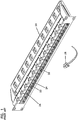
- FIG 1 shows a prior art panel 20 adapted for use with a twisted pair telecommunications system.
- the panel 20 includes a plurality ofjacks 22 placed in close proximity with one another.
- Each jack 22 includes a port 24 adapted to receive a standard telecommunications plug 26.
- Each of the jacks 22 is adapted to be terminated to four twisted pairs of transmission wires.
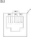
- each of the jacks 22 includes eight contact springs labeled as having positions 1-8.
- contact springs 4 and 5 are connected to a first pair of wires
- the contact springs 1 and 2 are connected to a second pair of wires
- contact springs 3 and 6 are connected to a third pair of wires
- contact springs 7 and 8 are connected to a fourth pair of wires.
- a typical plug 26 also has eight contacts (labeled 1-8) adapted to interconnect with the corresponding eight contacts of the jack 22 when the plug is inserted within the port 24.
- the contacts of the jacks and the plugs are required to be positioned in fairly close proximity to one another.
- the contact regions of the jacks and plugs are particularly susceptible to crosstalk.
- certain pairs of contacts are more susceptible to crosstalk than others.
- the first and third pairs of contacts in the plugs and jacks are typically most susceptible to crosstalk.
- jacks have been designed with contact spring configurations adapted to reduce the capacitive coupling generated between the contact springs so that crosstalk is minimized.
- An alternative approach involves intentionally generating crosstalk having a magnitude and phase designed to compensate for or correct crosstalk caused at the plug or jack.
- crosstalk compensation can be provided by manipulating the positioning of the contacts or leads of the jack or can be provided on a circuit board used to electrically connect the contact springs of the jack to insulation displacement connectors of the jack.
- US 2004/0082227 A1 teaches a method for compensating for alien crosstalk in a telecommunications jack with first and second capacitive elements having the same magnitude.
- US 2007/0238365 A1 teaches a telecommunications jack for use in a twisted pair system, the jack comprising:
- the technical problem is to provide an improved method for compensating for alien crosstalk in a telecommunications jack and to provide an improved telecommunications jack.
- the invention is defined by a method with the features of claim 1 and a telecommunications jack with the features of claim 6.
- the present disclosure relates to methods and systems for improving far end crosstalk compensation without adversely affecting near end crosstalk compensation within a telecommunications jack.
- the present disclosure generally describes crosstalk compensation schemes in which near end and far end crosstalk are accounted for and compensated against.
- the crosstalk compensation is achieved by use of at least two stages of capacitive compensation, in which the second stage is placed at an average time delay from the first stage such that near end crosstalk is optimized.
- the second stage has at least two capacitive elements spaced at different time delays from the first capacitive coupling to optimize far end crosstalk.
- the present disclosure also relates to methods and systems for compensating for alien crosstalk in a telecommunications jack.
- the present disclosure describes crosstalk compensation schemes in which alien crosstalk is compensated against, such as by selecting imbalanced capacitive arrangements across wire pairs to reduce the overall crosstalk experienced in a system, despite the potential for imbalanced compensation between wire pairs within a single jack.
- FIGS 4 and 5 show a telecommunications jack 120 (i.e., a telecommunications connector) having features that are examples of inventive aspects in accordance with the principles of the present disclosure.
- the jack 120 includes a dielectric housing 122 having a front piece 124 and a rear piece 126.
- the front and rear pieces 124, 126 can be interconnected by a snap fit connection.
- the front piece 124 defines a front port 128 sized and shaped to receive a conventional telecommunications plug (e.g., an RJ style plug such as an RJ 45 plug).
- the rear piece 126 defines an insulation displacement connector interface and includes a plurality of towers 130 adapted to house insulation displacement connector blades/contacts.
- the jack 120 further includes a circuit board 132 that mounts between the front and rear pieces 124, 126 of the housing 122.
- a plurality of contact springs CS 1 -CS 8 are terminated to a front side of the circuit board 132.
- a plurality of insulation displacement connector blades IDC 1 -IDC 8 are terminated to a back side of the circuit board 132.
- the contact springs CS 1 -CS 8 extend into the front port 128 and are adapted to be electrically connected to corresponding contacts provided on a plug when the plug is inserted into the front port 128.
- the insulation displacement connector blades IDC 1 -IDC 8 fit within the towers 130 of the rear piece 126 of the housing 122.
- the circuit board 132 has tracks T 1 -T 8 (e.g., tracings, see Figures 14-16 ) that respectively electrically connect the contact springs CS 1 -CS 8 to the insulation displacement connector blades IDC 1 -IDC 8 .
- wires are electrically connected to the contact springs CS 1 -CS 8 by inserting the wires between pairs of the insulation displacement connector blades IDC I -IDC 8 .
- the wires are inserted between pairs of the insulation displacement connector blades IDC 1 -IDC 8 , the blades cut through the insulation of the wires and make electrical contact with the center conductors of the wires.
- the insulation displacement connector blades IDC 1 -IDC 8 which are electrically connected to the contact springs CS 1 -CS 8 by the tracks on the circuit board, provide an efficient means for electrically connecting a twisted pair of wires to the contact springs CS 1 -CS 8 of the jack 120.
- the contact springs CS 1 -CS 8 are shown more clearly in Figures 6-8 .
- the relative positioning, shape and curvature of the contact springs CS 1 -CS 8 is preferably adapted to provide some initial crosstalk compensation at the jack 120.
- the circuit board 132 of the jack 120 is preferably a multiple layer circuit board.
- Figure 9 shows the circuit board 132 including a first conductive layer 140, a second conductive layer 142 and a third conductive layer 144.
- the first and second conductive layers 140, 142 are separated by a first dielectric layer 146.
- the second and third conductive layers 142, 144 are separated by a second dielectric layer 148.
- the first conductive layer 140 is located at a front side of the circuit board 132 and the third conductive layer 144 is located at a back side of the circuit board 132.
- the contact springs CS 1 -CS 8 are mounted at the front side of the circuit board 132, while the insulation displacement connector blades IDC 1 -IDC 8 are mounted at the back side of the circuit board 132. Vias extend through the first and second dielectric layers 146, 148 to provide electrical connections between the conductive layers 140, 142 and 144.
- the conductive layers 140, 142 and 144 are defined by electrically the conductive tracks T 1 -T 8 (see Figures 14-17 ).
- the tracks T 1 -T 8 are formed (e.g., etched or otherwise provided) on the dielectric layers 146, 148.
- the circuit board 132 preferably includes structures for compensating for near end crosstalk that occurs at the jack/plug interface.
- the structures for compensating for near end crosstalk include capacitive couplings provided between the first and second conductive layers 140, 142.
- the capacitive couplings are provided by sets of opposing, generally parallel capacitive plates located at the first and second conductive layers 140, 142. To increase the magnitude of the capacitive coupling provided between the capacitive plates of the first and second conductive layers 140, 142, it is desirable for the first dielectric layer 146 to be relatively thin.
- the first dielectric layer 146 can have a thickness t 1 less than about .01 inches (0,254 millimetres), or less than about .0075 inches (0,1905 millimetres), or less than about .005 inches (0,127 millimetres), or less than .003 inches (0,0762 millimetres).
- the thickness t 1 can be in the range of .001 inches (0,0254 millimetres) to .003 inches (0,0762 millimetres) or in the range of .001 inches (0,0254 millimetres) to .005 inches (0,127 millimetres). In a preferred embodiment, the thickness t 1 is about .002 inches (0,0508 millimetres).
- the first dielectric layer 146 can be made of a material having a relatively low dielectric constant.
- dielectric constants are dielectric constants relative to air.
- the dielectric constant of the first dielectric layer 146 can be equal to or less than about 5.
- the dielectric constant of the first dielectric layer 146 can be less than or equal to about 4 or less than or equal to about 3.
- An example material for manufacturing the first dielectric layer 146 is a flame resistant 4 (FR-4) circuit board material.
- FR-4 circuit board material is a composite of a resin epoxy reinforced with a woven fiberglass mat.
- the second dielectric layer 148 is preferably configured to isolate the third conductive layer 144 from the first and second conductive layers 140, 142.
- the second dielectric layer 148 can have a different thickness t 2 than the thickness t 1 of the first dielectric layer 146.
- the second dielectric layer 148 is at least 2.5 times thicker than the first dielectric layer 146 or at least five times thicker than the first dielectric layer 146.
- the second dielectric layer 148 is at least 10 times or at least 20 times thicker than the first dielectric layer 146.
- the thickness t 2 of the second dielectric layer 148 is in the range of .050 inches (1,27 millimetres) to .055 inches (1,397 millimetres).
- the thickness t 2 of the second dielectric layer 148 is in the range of .040 inches (1,016 millimetres) to .050 inches (1,27 millimetres).
- the second dielectric layer 148 can also be manufactured of a different material as compared to the first dielectric layer 146.
- the second dielectric layer can have different dielectric properties as compared to the first dielectric layer 146.
- the first dielectric layer 146 can have a dielectric constant that is greater (e.g., at least 1.5 times or at least 2 times greater) than the dielectric constant of the second dielectric layer 148.
- the second dielectric layer 148 can be manufactured of a material such as FR-4. Of course, it will be appreciated that other materials could also be used.
- the circuit board 132 includes a number of capacitive couplings having magnitudes and locations adapted to compensate for near end crosstalk and far end crosstalk. These forms of crosstalk are particularly problematic between the 4-5 and 3-6 pairs.
- three interdependent zones of compensation are used between tracks T 4-5 and tracks T 3-6 .
- the three interdependent zones of compensation include a first zone of compensation Z A1 , a second zone of compensation Z A2 and a third zone of compensation Z A3 .
- the first zone of compensation Z A1 includes a capacitive coupling C1 between track T 3 and track T 5 , and a capacitive coupling C2 between track T 4 and track T 6 .
- the second zone of compensation Z A2 includes a capacitive coupling C3 between track T 3 and track T 4 , and a capacitive coupling C4 between track T 5 and track T 6 .
- the third zone of compensation Z A3 includes a capacitive coupling C5 between track T 3 and track T 5 , and a capacitive coupling C6 between track T 4 and track T 6 .
- the capacitive couplings C3 and C4 are spaced apart, such that the average distance between the zones of compensation is as described below in Figure 11 , but the distances for the C3 and C4 couplings differ. As shown, coupling C3 is placed closer to the first zone of compensation Z A1 than coupling C4 while maintaining the average position of the zone Z A2 such that the distance between zones is as described below in Figure 11 .
- the capacitive couplings C1 and C2 are equal in magnitude and location, maintaining symmetry across the pairs.
- capacitive couplings C1 and C2 may be selected such that they differ in magnitude to compensate for alien crosstalk including the "excess" crosstalk previously mentioned, which is noted to be worst in the case of the 3-6 pair.
- changes to alien crosstalk can be made, both positively and negatively, by purposefully modifying the size of the compensating capacitors, causing them to become asymmetric in size and coupling.
- the magnitude of capacitor C1 is greater than the magnitude of capacitor C2, which can reduce the alien crosstalk generated at the 3-6 pair.
- Figure 11 is a schematic diagram representative of the compensation arrangement used to provide crosstalk compensation between the 4-5 and 3-6 pairs.
- the compensation arrangement includes a first vector 100, a second vector 102, a third vector 104, and a fourth vector 106.
- the first vector 100 and the third vector 104 have positive polarities, while the second vector 102 and the fourth vector 106 have negative polarities.
- the first vector 100 has a magnitude of M and corresponds to crosstalk introduced at the plug.
- the second vector 102 has a magnitude of about -3M and corresponds to the overall crosstalk introduced at the first zone of crosstalk Z A1 generated by the board and springs.
- the third vector 104 has a magnitude of about 3M and corresponds to the overall crosstalk introduced at the second zone of compensation Z A2 .
- the fourth vector 106 has a magnitude of about -M and corresponds to the overall crosstalk introduced at the third zone of compensation Z A3 . It will be appreciated that each vector is a lump sum of the total crosstalk or crosstalk compensation provided at each respective compensation zone, with the vectors being placed at the centers or midpoints of the compensation zones.
- the compensation scheme In designing the compensation scheme of Figure 11 , a number of factors are taken into consideration when determining the placement of the compensation zones.
- One factor includes the need to accommodate signal travel in both directions (i.e., in forward and reverse directions) through the tracks on the circuit board.
- the compensation scheme preferably has a configuration with forward and reverse symmetry. It is also desirable for the compensation scheme to provide optimized compensation over a relatively wide range of transmission frequencies. For example, in one embodiment, performance is optimized for frequencies ranging from 1 MHz to 500 MHz. It is further desirable for the compensation arrangement to take into consideration the phase shifts that occur as a result of the time delays that take place as signals travel between the zones of compensation.
- the second vector 102 is positioned as close as possible to the first vector 100.
- the time delay between the first vector 100 and the second vector 102 is shown as x.
- x can be about 100 picoseconds for a signal having a transmission speed of 3X10 8 meters per second.
- the time delay between the third vector 104 and the fourth vector 106 is preferred for the time delay between the third and fourth vectors to be approximately the same as the time delay between the first vector 100 and the second vector 102. As shown in Figure 11 , the time delay between the third and fourth vectors is depicted as x.
- the time delay y between the second vector 102 and the third vector 104 is preferably selected to optimize the overall compensation effect of the compensation scheme over a relatively wide range of frequencies.
- the phase angles of the first and second compensation zones are varied thereby altering the amount of compensation provided at different frequencies.
- the time delay y is initially set with a value generally equal to x (i.e., the time delay between the first vector 102 and the second vector 104). The system is then tested or simulated to determine if an acceptable level of compensation is provided across the entire signal frequency range intended to be used.
- the time delay y can be shortened to improve performance at higher frequencies. If the compensation scheme fails the near end crosstalk requirements at lower frequencies, the time delay y can be increased to improve crosstalk performance for lower frequencies. It will be appreciated that the time delay y can be varied without altering forward and reverse symmetry.
- the distance y is preferably greater than the distance x to provide optimized crosstalk compensation.
- the distance y is preferably less than the distance x to provide optimized crosstalk compensation.
- Crosstalk can also be an issue between the 1-2 and 3-6 pairs. Particularly, substantial crosstalk can be generated between track T 2 and track T 3 .
- a three-zone compensation arrangement is used to compensate for this crosstalk.
- the three-zone compensation arrangement includes a first zone of compensation Z B1 , a second zone of compensation Z B2 and a third zone of compensation Z B3 .
- the first zone of compensation Z B1 includes a capacitive coupling C7 between track T 1 and track T 3 , and a capacitive coupling C8 between track T 2 and track T 6 .
- the second zone of compensation Z B2 includes a capacitive coupling C9 between track T 1 and track T 6 .
- the third zone of compensation Z B3 includes a capacitive coupling C10 between track T 1 and track T 3 .
- the three zones of compensation between the 1-2 and 3-6 pairs can be placed at locations consistent with the vector diagram shown in Figure 11 , described above.
- varying the relative compensation among the pairs at the primary zones of compensation for each pair can affect alien crosstalk.
- zone of compensation Z B1 it has been determined that varying the relative magnitudes of the capacitive couplings C7 and C8, such that the capacitive couplings are non-equal, can improve overall alien crosstalk of the plug and jack system.
- a larger capacitance is used for capacitance C7 than C8, with the overall capacitance relating to the capacitive coupling introduced at the plug, as described above in conjunction with Figure 11 .
- zone of compensation Z B2 performance is optimized without use of a capacitive coupling between track T 2 and track T 3 .
- a capacitive coupling can be included to preserve symmetry between the pairs.
- no capacitive coupling is included between track T 2 and track T 6 , although in symmetric systems such a coupling could be included.
- the magnitudes of the compensation between the 3-6 and 4-5 pairs are substantially greater in magnitude than those between the 1-2 and 3-6 pairs.
- the compensation arrangement between the 4-5 and 7-8 pairs is a two zone compensation including a capacitive coupling C11 in a first zone Z C1 provided between track T 5 and track T 8 , and capacitive coupling C12 in a second zone Z C2 provided between track T 4 and track T 8 .
- Figure 12 is a schematic vector diagram showing the compensation arrangement used between the 4-5 and 7-8 pairs. As shown at Figure 12 , three crosstalk vectors are taken into consideration.
- the first crosstalk vector 110 is representative of crosstalk generated at the plug.
- a second vector 112 is representative of crosstalk provided at the first compensation zone Z C1 .
- the third vector 114 is representative of crosstalk generated at the second compensation zone Z C2 .
- the first and third vectors 110, 114 have positive polarities and magnitudes of about N.
- the second vector 112 has a negative polarity and a magnitude about 2N.
- the disclosed compensation arrangement is asymmetric among the pairs, a symmetric arrangement could be provided as well.
- M shown at Figure 11
- N shown at Figure 12
- varying the capacitive values across the 4-5 and 7-8 wire pairs used in the first zone of compensation Z C1 can improve alien crosstalk values generated from the plug-jack system.
- a completely unbalanced configuration is selected, such that Z C1 includes only compensation between track T 5 and track T 8 , with no corresponding balanced compensation between tracks T 4 and T 7 .
- a different, unbalanced arrangement may be selected.
- zone Z D1 is a single zone compensation used to compensate for crosstalk generated between the 1-2 and 4-5 pairs, and includes a capacitive coupling C13 provided between track T 2 and track T 5 .
- Another single zone compensation Z E1 compensates for crosstalk generated between the 3-6 and 7-8 pairs, and is provided by a capacitive coupling C14 formed between track T 3 and track T 7 .
- Other capacitive couplings may be included which compensate for unintended crosstalk generated within the board itself.
- zone Z D1 includes only compensation C13 between track T 2 and track T 5 , but no compensation between tracks track T 1 and track T 4 .
- zone Z E1 includes only compensation C14 between track T 3 and track T 7 , but no compensation between tracks track T 6 and track T 8 .
- the crosstalk compensation schemes illustrated herein generally are accomplished by first positioning a crosstalk compensation arrangement relating to crosstalk within the plug and jack, across a variety of wire pairs.
- a designer will generally first locate a first zone of capacitive coupling a first time delay away from the capacitive coupling at the plug.
- the designer can then position a second capacitive coupling, i.e. a second zone of compensation, at a second time delay away from the first time delay.
- That second zone of compensation can be made up of more than one capacitive coupling, and can have capacitive couplings of differing magnitude.
- two capacitors can make up a zone of compensation, and can be placed at differing distances from a first zone.
- An example of such a configuration is illustrated by zone Z A2 as described above.
- the compensation arrangement can be altered to improve alien crosstalk. Altering the compensation arrangement is performed to accommodate one or more zones of crosstalk compensation having an asymmetric capacitive coupling between a wire pairs, such that alien crosstalk is reduced. This can be performed by changing the relative magnitudes of the capacitive couplings between wire pairs in one or more of the zones of compensation.
- a designer can start with a compensation arrangement having symmetric capacitive couplings across complementary wire pairs (e.g. from the 3-6 pair to the 4-5 pair, having equal couplings between T 3 and T 5 and between T 4 and T 6) .
- any amount of asymmetry in any zone of compensation can be introduced to compensate for alien crosstalk, from complete symmetry to complete asymmetry.
- the various asymmetric capacitive coupling selections made to account for alien crosstalk are believed to, as a whole, compensate for crosstalk generated in an overall system including both a plug and a contact set of a modular jack, as described above in Figures 4-7 .
- the crosstalk compensations selected in the present disclosure may not be symmetric in the sense that equal capacitive couplings are not applied across complementary tracks of a wire pair. Although this may have the effect of slightly worse performance with respect to connector balance and crosstalk within the pair, the net effect of a number of plug and jack systems in close proximity is an improved overall crosstalk compensation.
- Figures 13-16 show an example circuit board layout for implementing the compensation arrangement of Figure 10 .
- Figures 14-16 respectively show the front, middle and back conductive layers 140, 142 and 144 of the circuit board 132.
- Figure 13 is an overlay of the three conductive layers 140, 142 and 144.
- the circuit board 132 defines openings 301-308 that respectively receive posts of the contact springs CS 1 -CS 8 so that the contact springs CS 1 -CS 8 are terminated to the board 132.
- the circuit board also defines openings 401-408 for respectively receiving posts of the insulation displacement connector blades IDC 1 -IDC 8 such that the insulation displacement connector blades IDC 1 -IDC 8 are terminated to the circuit board.
- Vias extend through the circuit board for electrically interconnecting the tracks between the layers 140, 142 and 144, and to the various capacitive couplings C1-C13.
- vias V 4A and V 4B interconnect the portions of the track T 4 located at the different layers 140, 142 and 144 to the capacitive couplings C3 and C6.
- via V 5 interconnects the portions of the track T 5 located at the different layers 140, 142 and 144 to capacitive coupling C5.
- via V 6 interconnects the portions of the track T 6 located at the different layers 140, 142 and 144 with capacitive coupling C6.
- via V 3 interconnects the portions of the track T 3 located at the different layers 140, 142 and 144 to capacitive coupling C5.
- the capacitive coupling C1 of the first zone of compensation Z A1 is provided by opposing capacitor plates C1 5 and C1 3 respectively provided at layers 142 and 144.
- the capacitive coupling C2 of the first zone of compensation Z A1 is provided by opposing capacitor plates C2 4 and C2 6 that are respectively provided at the layers 142 and 144.
- the capacitive coupling C3 of the second compensation zone Z A2 is provided by opposing capacitor plates C3 4 and C3 3 that are respectively provided at layers 142 and 144.
- the capacitive coupling C4 of the second compensation zone Z A2 is provided by opposing capacitor plates C4 6 and C4 5 that are respectively provided at layers 142 and 144.
- the capacitive coupling C5 of the third compensation zone Z A3 is provided by a capacitor plate C5 5A that is provided at layer 142.
- the capacitive coupling C5 is also provided by inter-digitated capacitor fingers C5 5B and C5 3B that are provided at layer 140.
- the capacitive coupling C6 of the second compensation zone Z A3 is provided by capacitor plate C6 6A provided at layer 142.
- the capacitive coupling C6 is also provided by inter-digitated capacitor fingers C6 6B and C6 4B provided at layer 140.
- the capacitive coupling C7 of the first compensation zone Z B1 is provided by opposing capacitor plates C7 1 and C7 3 that are respectively provided at layers 142 and 144 of the circuit board.
- the capacitive coupling C8 of the first compensation zone Z B1 is provided by opposing capacitor plates C8 2 and C8 6 that are respectively provided at the layers 142 and 144 of the circuit board.
- the capacitive coupling C9 of the second zone of compensation Z B2 is provided by opposing capacitor plates C9 1 and C9 6 that are respectively provided at layer 142 and 144 of the circuit board.
- the capacitive coupling C10 of the third zone of compensation Z B3 is provided by opposing capacitor plates C10 1 and C10 3 that are respectively provided at layers 142 and 144 of the circuit board.
- the capacitive coupling C11 of the first compensation zone Z C1 is provided by opposing capacitor plates C11 5 and C11 8 that are respectively provided at layers 142 and 144 of the circuit board.
- the capacitive coupling C12 of the second compensation zone ZC2 is provided by adjacent leads C124 and C128, respectively, located at layer 142.
- the capacitive coupling C13 of the zone of compensation Zm is provided by opposing capacitor plates Cl3 2 and Cl3 5 provided at layers 142 and 144 of the circuit board.
- the capacitive coupling C14 of the zone of compensation ZEI is provided by opposing capacitor plates C14 7 and C14 3 respectively provided at layers 142 and 144 of the circuit board.
Landscapes
- Physics & Mathematics (AREA)
- Electromagnetism (AREA)
- Engineering & Computer Science (AREA)
- Microelectronics & Electronic Packaging (AREA)
- Details Of Connecting Devices For Male And Female Coupling (AREA)
Claims (10)
- Verfahren zum Kompensieren von Fremdübersprechen an einem oder mehreren einer Vielzahl von Drahtpaaren (1-2/3-6/4-5/7-8) in einer Telekommunikationsbuchse (120), das Verfahren weist auf:Positionieren einer Übersprechungskompensationsanordnung bezüglich Übersprechen über zumindest ein erstes Drahtpaar (1-2/3-6/4-5) und ein zweites Drahtpaar (3-6/4-5/7-8) auf einer Leiterplatte (132) innerhalb einer Telekommunikationsbuchse (120), wobei die Übersprechungskompensationsanordnung eine Vielzahl von symmetrischen Zonen einer Übersprechungskompensation (ZA1/ZA2/ZA3/ZB1/ZB2/ZB3/ZC1/ZC2/ZD1/ZE1) zwischen einem ersten Drahtpaar (1-2/3-6/4-5) und einem zweiten Drahtpaar (3-6/4-5/7-8) enthält; undÄndern der Übersprechungskompensationsanordnung in zumindest einer der Vielzahl von Zonen einer Übersprechungskompensation (ZA1/ZA2/ZA3/ZB1/ZB2/ZB3/ZC1/ZC2/ZD1/ZE1), die Kontaktfedern (CS1-CS8) des ersten Drahtpaares (1-2/3-6/4-5) und des zweiten Drahtpaares (3-6/4-5/7-8) am nächsten ist, um eine asymmetrische kapazitive Kopplung (C1-C14) zwischen dem ersten Drahtpaar (1-2/3-6/4-5) und dem zweiten Drahtpaar (3-6/4-5/7-8) bereitzustellen, um Fremdübersprechen an einem des ersten und zweiten Drahtpaares (1-2/3-6/4-5/7-8) zu verringern.
- Verfahren nach Anspruch 1, wobei Ändern der Übersprechungskompensationsanordnung ein Auswählen einer Kompensationsanordnung aufweist, die im Wesentlichen das gesamte Gleichgewicht eines Systems verbessert, das die Telekommunikationsbuchse (120) und einen Stecker (26) enthält, der elektrisch mit der Telekommunikationsbuchse (120) verbunden ist.
- Verfahren nach Anspruch 1, wobei die Kompensationsanordnung von mindestens einer der Vielzahl von Zonen einer Übersprechungskompensation (ZA1/ZA2/ZA3/ZB1/ZB2/ZB3/ZC1/ZC2/ZD1/ZE1) voll kommen asymmetrisch in Bezug auf mindestens eines des ersten und zweiten Drahtpaares (1-2/3-6/4-5/7-8) ist.
- Verfahren nach Anspruch 1, wobei die Kompensationsanordnung asymmetrische Kompensation enthält, die über zumindest eine Leiterbahn (T1-T8) von zwei oder mehr Drahtpaaren (1-2/3-6/4-5/7-8) angeordnet ist, die elektrisch durch die Telekommunikationsbuchse (120) verbunden sind.
- Verfahren nach Anspruch 1, wobei mindestens eine der Vielzahl von Zonen einer Übersprechungskompensation (ZA1/ZA2/ZA3/ZB1/ZB2/ZB3/ZC1/ZC2) zwei kapazitive Elemente (C1-C12) enthält, die zwischen Drähten eines ersten Drahtpaares (1-2/3-6/4-5) und eines zweiten Drahtpaares (3-6/4-5/7-8) verbunden sind.
- Telekommunikationsbuchse (120) zur Verwendung in einem verdrillten Paarsystem, wobei die Buchse (120) aufweist:ein Gehäuse (122), das einen Anschluss (24/118) zum Aufnehmen eines Steckers (26) definiert;eine Vielzahl von Kontaktfedern (CS1-CS8), die ausgebildet sind, elektrischen Kontakt mit dem Stecker (26) herzustellen, wenn der Stecker (26) in den Anschluss (24/128) des Gehäuses (122) eingesetzt ist;eine Vielzahl von Drahtanschlusskontakten (IDC1-IDC8) zum Anschließen von Drähten an die Buchse (120) ;eine Leiterplatte (132), die leitfähige Leiterbahnen (T1-T8) enthält, die die Kontaktfedern (CS1-CS8) elektrisch mit den Drahtanschlusskontakten (IDC1-IDC8) verbinden; undeine Übersprechungskompensationsanordnung, die Übersprechungskompensation zwischen ausgewählten Leiterbahnen (T1-T8) der Leiterplatte (132) bereitstellt, wobei die Übersprechungskompensationsanordnung eine Vielzahl von Zonen einer Übersprechungskompensation (ZB1, ZB2, ZB3, ZC1, ZC2, ZD1, ZE1) enthält, die eine erste Zone mit einer asymmetrischen kapazitiven Kopplung (C1, C2; C5, [[-]],C6) zwischen einem ersten Drahtpaar (3-6) und einem zweiten Drahtpaar (4-5) und eine zweite Zone (ZB1) mit einer asymmetrischen kapazitiven Kopplung (C7, C8) zwischen einem dritten Drahtpaar (1-2) und dem ersten Drahtpaar (3-6) enthalten,wobei die Telekommunikationsbuchse dadurch gekennzeichnet ist, dass eine der ersten und zweiten Zonen einer Übersprechungskompensation am nächsten zu den Kontaktfedern (CS1-CS8) angeordnet ist, die mit dem ersten Drahtpaar (3-6) und dem zweiten Drahtpaar (4-5) assoziiert sind, und angeordnet ist, Fremdübersprechen von mindestens einem des ersten, zweiten und dritten Drahtpaares (1-2/3-6/4-5/7-8) zu verringern, wobei Fremdübersprechen mit einer benachbarten Telekommunikationsbuchse verringert wird,wobei zumindest eine der Vielzahl von Zonen einer Übersprechungskompensation (ZA1) ein erstes und ein zweites kapazitives Element (C1,C2;C7,C8) enthält, das zwischen den Drähten von zumindest einem von 1) dem ersten Drahtpaar (3-6) und dem zweiten Drahtpaar (4-5) und 2) dem dritten Drahtpaar (1-2) und dem ersten Drahtpaar (3-6) verbunden ist, wobei das zweite kapazitive Element eine kleinere Magnitude als das erste kapazitive Element aufweist.
- Telekommunikationsbuchse (120) nach Anspruch 6, wobei die zwei kapazitiven Elemente (C1-C8) verschiedene Drähte des ersten Drahtpaares (3-6) und des zweiten Drahtpaares (4-5) verbinden.
- Telekommunikationsbuchse (120) nach Anspruch 7, wobei mindestens eine Zone einer Übersprechungskompensation (ZA1/ZA2/ZA3/ZB1/ZB2/ZB3/ZC2/ZC2/ZD1/ZE1) in Bezug auf mindestens eines des ersten und zweiten Drahtpaares (3-6/4-5) vollkommen asymmetrisch ist.
- Telekommunikationsbuchse (120) nach Anspruch 7, wobei die Übersprechungskompensationsanordnung zwei oder mehr Zonen einer Übersprechungskompensation (ZA1/ZA2/ZA3/ZB1/ZB2/ZB3/ZC1/ZC2/ZD1/ZE1) enthält.
- Telekommunikationsbuchse (120) nach Anspruch 7, wobei die Kompensationsanordnung im Wesentlichen das gesamte Gleichgewicht eines Systems verbessert, das die Telekommunikationsbuchse (120) und einen Stecker (26) enthält, der elektrisch mit der Telekommunikationsbuchse (120) verbunden ist.
Applications Claiming Priority (3)
| Application Number | Priority Date | Filing Date | Title |
|---|---|---|---|
| US2803208P | 2008-02-12 | 2008-02-12 | |
| US12/369,532 US7798857B2 (en) | 2008-02-12 | 2009-02-11 | Asymmetric crosstalk compensation for improved alien crosstalk performance |
| PCT/US2009/033890 WO2009102849A1 (en) | 2008-02-12 | 2009-02-12 | Asymmetric crosstalk compensation for improved alien crosstalk performance |
Publications (2)
| Publication Number | Publication Date |
|---|---|
| EP2243201A1 EP2243201A1 (de) | 2010-10-27 |
| EP2243201B1 true EP2243201B1 (de) | 2019-11-27 |
Family
ID=40639743
Family Applications (1)
| Application Number | Title | Priority Date | Filing Date |
|---|---|---|---|
| EP09710121.6A Active EP2243201B1 (de) | 2008-02-12 | 2009-02-12 | Asymmetrische übersprechkompensation für verbesserte fremd-übersprechleistungsfähigkeit |
Country Status (6)
| Country | Link |
|---|---|
| US (1) | US7798857B2 (de) |
| EP (1) | EP2243201B1 (de) |
| AU (1) | AU2009214686B2 (de) |
| IL (1) | IL205598A0 (de) |
| WO (1) | WO2009102849A1 (de) |
| ZA (1) | ZA201005717B (de) |
Families Citing this family (6)
| Publication number | Priority date | Publication date | Assignee | Title |
|---|---|---|---|---|
| US7381098B2 (en) | 2006-04-11 | 2008-06-03 | Adc Telecommunications, Inc. | Telecommunications jack with crosstalk multi-zone crosstalk compensation and method for designing |
| US7841909B2 (en) | 2008-02-12 | 2010-11-30 | Adc Gmbh | Multistage capacitive far end crosstalk compensation arrangement |
| CN102124609B (zh) * | 2008-08-20 | 2013-09-11 | 泛达公司 | 具有多级补偿的高速连接器 |
| US8167661B2 (en) * | 2008-12-02 | 2012-05-01 | Panduit Corp. | Method and system for improving crosstalk attenuation within a plug/jack connection and between nearby plug/jack combinations |
| CN102346787B (zh) * | 2010-07-29 | 2015-04-08 | 中山市云创知识产权服务有限公司 | 信号线串扰信息检查系统及方法 |
| WO2014144735A1 (en) | 2013-03-15 | 2014-09-18 | Tyco Electronics Uk Ltd. | Connector with capacitive crosstalk compensation to reduce alien crosstalk |
Family Cites Families (7)
| Publication number | Priority date | Publication date | Assignee | Title |
|---|---|---|---|---|
| USRE38519E1 (en) * | 1998-08-24 | 2004-05-18 | Panduit Corp. | Low crosstalk modular communication connector |
| US6089923A (en) * | 1999-08-20 | 2000-07-18 | Adc Telecommunications, Inc. | Jack including crosstalk compensation for printed circuit board |
| US6866548B2 (en) * | 2002-10-23 | 2005-03-15 | Avaya Technology Corp. | Correcting for near-end crosstalk unbalance caused by deployment of crosstalk compensation on other pairs |
| US20050221678A1 (en) * | 2004-02-20 | 2005-10-06 | Hammond Bernard Jr | Methods and systems for compensating for alien crosstalk between connectors |
| US7190594B2 (en) * | 2004-05-14 | 2007-03-13 | Commscope Solutions Properties, Llc | Next high frequency improvement by using frequency dependent effective capacitance |
| US7175476B2 (en) * | 2005-01-11 | 2007-02-13 | Daeun Electronics Co., Ltd. | Crosstalk canceling pattern for high-speed communications and modular jack having the same |
| US7402085B2 (en) * | 2006-04-11 | 2008-07-22 | Adc Gmbh | Telecommunications jack with crosstalk compensation provided on a multi-layer circuit board |
-
2009
- 2009-02-11 US US12/369,532 patent/US7798857B2/en active Active
- 2009-02-12 AU AU2009214686A patent/AU2009214686B2/en not_active Ceased
- 2009-02-12 WO PCT/US2009/033890 patent/WO2009102849A1/en not_active Ceased
- 2009-02-12 EP EP09710121.6A patent/EP2243201B1/de active Active
-
2010
- 2010-05-06 IL IL205598A patent/IL205598A0/en unknown
- 2010-08-11 ZA ZA2010/05717A patent/ZA201005717B/en unknown
Non-Patent Citations (1)
| Title |
|---|
| None * |
Also Published As
| Publication number | Publication date |
|---|---|
| WO2009102849A1 (en) | 2009-08-20 |
| AU2009214686B2 (en) | 2015-01-15 |
| ZA201005717B (en) | 2011-04-28 |
| IL205598A0 (en) | 2010-11-30 |
| AU2009214686A1 (en) | 2009-08-20 |
| US7798857B2 (en) | 2010-09-21 |
| US20090258541A1 (en) | 2009-10-15 |
| EP2243201A1 (de) | 2010-10-27 |
Similar Documents
| Publication | Publication Date | Title |
|---|---|---|
| US12424794B2 (en) | Multistage capacitive crosstalk compensation arrangement | |
| US11264764B2 (en) | Telecommunications device | |
| EP2008346B1 (de) | Telekommunikationsbuchse mit Übersprechungskompensation und Anordnungen zur Minderung von Reflexionsverlusten | |
| EP2243201B1 (de) | Asymmetrische übersprechkompensation für verbesserte fremd-übersprechleistungsfähigkeit | |
| AU2015200609B2 (en) | Improved far end crosstalk compensation |
Legal Events
| Date | Code | Title | Description |
|---|---|---|---|
| PUAI | Public reference made under article 153(3) epc to a published international application that has entered the european phase |
Free format text: ORIGINAL CODE: 0009012 |
|
| 17P | Request for examination filed |
Effective date: 20100416 |
|
| AK | Designated contracting states |
Kind code of ref document: A1 Designated state(s): AT BE BG CH CY CZ DE DK EE ES FI FR GB GR HR HU IE IS IT LI LT LU LV MC MK MT NL NO PL PT RO SE SI SK TR |
|
| AX | Request for extension of the european patent |
Extension state: AL BA RS |
|
| DAX | Request for extension of the european patent (deleted) | ||
| RAP1 | Party data changed (applicant data changed or rights of an application transferred) |
Owner name: TYCO ELECTRONICS AMP GMBH |
|
| RAP1 | Party data changed (applicant data changed or rights of an application transferred) |
Owner name: TYCO ELECTRONICS SERVICES GMBH |
|
| 17Q | First examination report despatched |
Effective date: 20150223 |
|
| RAP1 | Party data changed (applicant data changed or rights of an application transferred) |
Owner name: COMMSCOPE EMEA LIMITED |
|
| RAP1 | Party data changed (applicant data changed or rights of an application transferred) |
Owner name: COMMSCOPE TECHNOLOGIES LLC |
|
| STAA | Information on the status of an ep patent application or granted ep patent |
Free format text: STATUS: EXAMINATION IS IN PROGRESS |
|
| REG | Reference to a national code |
Ref country code: DE Ref legal event code: R079 Ref document number: 602009060542 Country of ref document: DE Free format text: PREVIOUS MAIN CLASS: H01R0024040000 Ipc: H01R0013646600 |
|
| GRAP | Despatch of communication of intention to grant a patent |
Free format text: ORIGINAL CODE: EPIDOSNIGR1 |
|
| STAA | Information on the status of an ep patent application or granted ep patent |
Free format text: STATUS: GRANT OF PATENT IS INTENDED |
|
| RIC1 | Information provided on ipc code assigned before grant |
Ipc: H01R 13/6466 20110101AFI20190516BHEP |
|
| INTG | Intention to grant announced |
Effective date: 20190619 |
|
| GRAS | Grant fee paid |
Free format text: ORIGINAL CODE: EPIDOSNIGR3 |
|
| GRAA | (expected) grant |
Free format text: ORIGINAL CODE: 0009210 |
|
| STAA | Information on the status of an ep patent application or granted ep patent |
Free format text: STATUS: THE PATENT HAS BEEN GRANTED |
|
| AK | Designated contracting states |
Kind code of ref document: B1 Designated state(s): AT BE BG CH CY CZ DE DK EE ES FI FR GB GR HR HU IE IS IT LI LT LU LV MC MK MT NL NO PL PT RO SE SI SK TR |
|
| REG | Reference to a national code |
Ref country code: GB Ref legal event code: FG4D |
|
| REG | Reference to a national code |
Ref country code: CH Ref legal event code: EP |
|
| REG | Reference to a national code |
Ref country code: AT Ref legal event code: REF Ref document number: 1207778 Country of ref document: AT Kind code of ref document: T Effective date: 20191215 |
|
| REG | Reference to a national code |
Ref country code: DE Ref legal event code: R096 Ref document number: 602009060542 Country of ref document: DE |
|
| REG | Reference to a national code |
Ref country code: IE Ref legal event code: FG4D |
|
| REG | Reference to a national code |
Ref country code: NL Ref legal event code: MP Effective date: 20191127 |
|
| REG | Reference to a national code |
Ref country code: LT Ref legal event code: MG4D |
|
| PG25 | Lapsed in a contracting state [announced via postgrant information from national office to epo] |
Ref country code: ES Free format text: LAPSE BECAUSE OF FAILURE TO SUBMIT A TRANSLATION OF THE DESCRIPTION OR TO PAY THE FEE WITHIN THE PRESCRIBED TIME-LIMIT Effective date: 20191127 Ref country code: NL Free format text: LAPSE BECAUSE OF FAILURE TO SUBMIT A TRANSLATION OF THE DESCRIPTION OR TO PAY THE FEE WITHIN THE PRESCRIBED TIME-LIMIT Effective date: 20191127 Ref country code: LT Free format text: LAPSE BECAUSE OF FAILURE TO SUBMIT A TRANSLATION OF THE DESCRIPTION OR TO PAY THE FEE WITHIN THE PRESCRIBED TIME-LIMIT Effective date: 20191127 Ref country code: NO Free format text: LAPSE BECAUSE OF FAILURE TO SUBMIT A TRANSLATION OF THE DESCRIPTION OR TO PAY THE FEE WITHIN THE PRESCRIBED TIME-LIMIT Effective date: 20200227 Ref country code: BG Free format text: LAPSE BECAUSE OF FAILURE TO SUBMIT A TRANSLATION OF THE DESCRIPTION OR TO PAY THE FEE WITHIN THE PRESCRIBED TIME-LIMIT Effective date: 20200227 Ref country code: GR Free format text: LAPSE BECAUSE OF FAILURE TO SUBMIT A TRANSLATION OF THE DESCRIPTION OR TO PAY THE FEE WITHIN THE PRESCRIBED TIME-LIMIT Effective date: 20200228 Ref country code: FI Free format text: LAPSE BECAUSE OF FAILURE TO SUBMIT A TRANSLATION OF THE DESCRIPTION OR TO PAY THE FEE WITHIN THE PRESCRIBED TIME-LIMIT Effective date: 20191127 Ref country code: SE Free format text: LAPSE BECAUSE OF FAILURE TO SUBMIT A TRANSLATION OF THE DESCRIPTION OR TO PAY THE FEE WITHIN THE PRESCRIBED TIME-LIMIT Effective date: 20191127 Ref country code: LV Free format text: LAPSE BECAUSE OF FAILURE TO SUBMIT A TRANSLATION OF THE DESCRIPTION OR TO PAY THE FEE WITHIN THE PRESCRIBED TIME-LIMIT Effective date: 20191127 |
|
| PG25 | Lapsed in a contracting state [announced via postgrant information from national office to epo] |
Ref country code: IS Free format text: LAPSE BECAUSE OF FAILURE TO SUBMIT A TRANSLATION OF THE DESCRIPTION OR TO PAY THE FEE WITHIN THE PRESCRIBED TIME-LIMIT Effective date: 20200327 Ref country code: HR Free format text: LAPSE BECAUSE OF FAILURE TO SUBMIT A TRANSLATION OF THE DESCRIPTION OR TO PAY THE FEE WITHIN THE PRESCRIBED TIME-LIMIT Effective date: 20191127 |
|
| PG25 | Lapsed in a contracting state [announced via postgrant information from national office to epo] |
Ref country code: CZ Free format text: LAPSE BECAUSE OF FAILURE TO SUBMIT A TRANSLATION OF THE DESCRIPTION OR TO PAY THE FEE WITHIN THE PRESCRIBED TIME-LIMIT Effective date: 20191127 Ref country code: RO Free format text: LAPSE BECAUSE OF FAILURE TO SUBMIT A TRANSLATION OF THE DESCRIPTION OR TO PAY THE FEE WITHIN THE PRESCRIBED TIME-LIMIT Effective date: 20191127 Ref country code: DK Free format text: LAPSE BECAUSE OF FAILURE TO SUBMIT A TRANSLATION OF THE DESCRIPTION OR TO PAY THE FEE WITHIN THE PRESCRIBED TIME-LIMIT Effective date: 20191127 Ref country code: EE Free format text: LAPSE BECAUSE OF FAILURE TO SUBMIT A TRANSLATION OF THE DESCRIPTION OR TO PAY THE FEE WITHIN THE PRESCRIBED TIME-LIMIT Effective date: 20191127 Ref country code: PT Free format text: LAPSE BECAUSE OF FAILURE TO SUBMIT A TRANSLATION OF THE DESCRIPTION OR TO PAY THE FEE WITHIN THE PRESCRIBED TIME-LIMIT Effective date: 20200419 |
|
| REG | Reference to a national code |
Ref country code: DE Ref legal event code: R097 Ref document number: 602009060542 Country of ref document: DE |
|
| PG25 | Lapsed in a contracting state [announced via postgrant information from national office to epo] |
Ref country code: SK Free format text: LAPSE BECAUSE OF FAILURE TO SUBMIT A TRANSLATION OF THE DESCRIPTION OR TO PAY THE FEE WITHIN THE PRESCRIBED TIME-LIMIT Effective date: 20191127 |
|
| REG | Reference to a national code |
Ref country code: DE Ref legal event code: R119 Ref document number: 602009060542 Country of ref document: DE |
|
| REG | Reference to a national code |
Ref country code: AT Ref legal event code: MK05 Ref document number: 1207778 Country of ref document: AT Kind code of ref document: T Effective date: 20191127 |
|
| REG | Reference to a national code |
Ref country code: CH Ref legal event code: PL |
|
| PLBE | No opposition filed within time limit |
Free format text: ORIGINAL CODE: 0009261 |
|
| STAA | Information on the status of an ep patent application or granted ep patent |
Free format text: STATUS: NO OPPOSITION FILED WITHIN TIME LIMIT |
|
| REG | Reference to a national code |
Ref country code: BE Ref legal event code: MM Effective date: 20200229 |
|
| PG25 | Lapsed in a contracting state [announced via postgrant information from national office to epo] |
Ref country code: LU Free format text: LAPSE BECAUSE OF NON-PAYMENT OF DUE FEES Effective date: 20200212 Ref country code: MC Free format text: LAPSE BECAUSE OF FAILURE TO SUBMIT A TRANSLATION OF THE DESCRIPTION OR TO PAY THE FEE WITHIN THE PRESCRIBED TIME-LIMIT Effective date: 20191127 |
|
| 26N | No opposition filed |
Effective date: 20200828 |
|
| PG25 | Lapsed in a contracting state [announced via postgrant information from national office to epo] |
Ref country code: PL Free format text: LAPSE BECAUSE OF FAILURE TO SUBMIT A TRANSLATION OF THE DESCRIPTION OR TO PAY THE FEE WITHIN THE PRESCRIBED TIME-LIMIT Effective date: 20191127 Ref country code: SI Free format text: LAPSE BECAUSE OF FAILURE TO SUBMIT A TRANSLATION OF THE DESCRIPTION OR TO PAY THE FEE WITHIN THE PRESCRIBED TIME-LIMIT Effective date: 20191127 Ref country code: AT Free format text: LAPSE BECAUSE OF FAILURE TO SUBMIT A TRANSLATION OF THE DESCRIPTION OR TO PAY THE FEE WITHIN THE PRESCRIBED TIME-LIMIT Effective date: 20191127 Ref country code: LI Free format text: LAPSE BECAUSE OF NON-PAYMENT OF DUE FEES Effective date: 20200229 Ref country code: CH Free format text: LAPSE BECAUSE OF NON-PAYMENT OF DUE FEES Effective date: 20200229 |
|
| PG25 | Lapsed in a contracting state [announced via postgrant information from national office to epo] |
Ref country code: DE Free format text: LAPSE BECAUSE OF NON-PAYMENT OF DUE FEES Effective date: 20200901 Ref country code: IE Free format text: LAPSE BECAUSE OF NON-PAYMENT OF DUE FEES Effective date: 20200212 Ref country code: IT Free format text: LAPSE BECAUSE OF FAILURE TO SUBMIT A TRANSLATION OF THE DESCRIPTION OR TO PAY THE FEE WITHIN THE PRESCRIBED TIME-LIMIT Effective date: 20191127 |
|
| PG25 | Lapsed in a contracting state [announced via postgrant information from national office to epo] |
Ref country code: BE Free format text: LAPSE BECAUSE OF NON-PAYMENT OF DUE FEES Effective date: 20200229 |
|
| PG25 | Lapsed in a contracting state [announced via postgrant information from national office to epo] |
Ref country code: TR Free format text: LAPSE BECAUSE OF FAILURE TO SUBMIT A TRANSLATION OF THE DESCRIPTION OR TO PAY THE FEE WITHIN THE PRESCRIBED TIME-LIMIT Effective date: 20191127 Ref country code: MT Free format text: LAPSE BECAUSE OF FAILURE TO SUBMIT A TRANSLATION OF THE DESCRIPTION OR TO PAY THE FEE WITHIN THE PRESCRIBED TIME-LIMIT Effective date: 20191127 Ref country code: CY Free format text: LAPSE BECAUSE OF FAILURE TO SUBMIT A TRANSLATION OF THE DESCRIPTION OR TO PAY THE FEE WITHIN THE PRESCRIBED TIME-LIMIT Effective date: 20191127 |
|
| PG25 | Lapsed in a contracting state [announced via postgrant information from national office to epo] |
Ref country code: MK Free format text: LAPSE BECAUSE OF FAILURE TO SUBMIT A TRANSLATION OF THE DESCRIPTION OR TO PAY THE FEE WITHIN THE PRESCRIBED TIME-LIMIT Effective date: 20191127 |
|
| PGFP | Annual fee paid to national office [announced via postgrant information from national office to epo] |
Ref country code: FR Payment date: 20230223 Year of fee payment: 15 |
|
| PGFP | Annual fee paid to national office [announced via postgrant information from national office to epo] |
Ref country code: GB Payment date: 20230227 Year of fee payment: 15 |
|
| P01 | Opt-out of the competence of the unified patent court (upc) registered |
Effective date: 20230530 |
|
| GBPC | Gb: european patent ceased through non-payment of renewal fee |
Effective date: 20240212 |
|
| PG25 | Lapsed in a contracting state [announced via postgrant information from national office to epo] |
Ref country code: GB Free format text: LAPSE BECAUSE OF NON-PAYMENT OF DUE FEES Effective date: 20240212 |
|
| PG25 | Lapsed in a contracting state [announced via postgrant information from national office to epo] |
Ref country code: FR Free format text: LAPSE BECAUSE OF NON-PAYMENT OF DUE FEES Effective date: 20240229 |
|
| PG25 | Lapsed in a contracting state [announced via postgrant information from national office to epo] |
Ref country code: GB Free format text: LAPSE BECAUSE OF NON-PAYMENT OF DUE FEES Effective date: 20240212 Ref country code: FR Free format text: LAPSE BECAUSE OF NON-PAYMENT OF DUE FEES Effective date: 20240229 |