EP2242092A1 - Plasma processing method and plasma processing system - Google Patents
Plasma processing method and plasma processing system Download PDFInfo
- Publication number
- EP2242092A1 EP2242092A1 EP09705243A EP09705243A EP2242092A1 EP 2242092 A1 EP2242092 A1 EP 2242092A1 EP 09705243 A EP09705243 A EP 09705243A EP 09705243 A EP09705243 A EP 09705243A EP 2242092 A1 EP2242092 A1 EP 2242092A1
- Authority
- EP
- European Patent Office
- Prior art keywords
- plasma processing
- bias power
- film
- substrate
- processing method
- Prior art date
- Legal status (The legal status is an assumption and is not a legal conclusion. Google has not performed a legal analysis and makes no representation as to the accuracy of the status listed.)
- Withdrawn
Links
Images



Classifications
-
- H—ELECTRICITY
- H10—SEMICONDUCTOR DEVICES; ELECTRIC SOLID-STATE DEVICES NOT OTHERWISE PROVIDED FOR
- H10P—GENERIC PROCESSES OR APPARATUS FOR THE MANUFACTURE OR TREATMENT OF DEVICES COVERED BY CLASS H10
- H10P14/00—Formation of materials, e.g. in the shape of layers or pillars
- H10P14/60—Formation of materials, e.g. in the shape of layers or pillars of insulating materials
- H10P14/69—Inorganic materials
- H10P14/694—Inorganic materials composed of nitrides
- H10P14/6943—Inorganic materials composed of nitrides containing silicon
- H10P14/69433—Inorganic materials composed of nitrides containing silicon the material being a silicon nitride not containing oxygen, e.g. SixNy or SixByNz
-
- C—CHEMISTRY; METALLURGY
- C23—COATING METALLIC MATERIAL; COATING MATERIAL WITH METALLIC MATERIAL; CHEMICAL SURFACE TREATMENT; DIFFUSION TREATMENT OF METALLIC MATERIAL; COATING BY VACUUM EVAPORATION, BY SPUTTERING, BY ION IMPLANTATION OR BY CHEMICAL VAPOUR DEPOSITION, IN GENERAL; INHIBITING CORROSION OF METALLIC MATERIAL OR INCRUSTATION IN GENERAL
- C23C—COATING METALLIC MATERIAL; COATING MATERIAL WITH METALLIC MATERIAL; SURFACE TREATMENT OF METALLIC MATERIAL BY DIFFUSION INTO THE SURFACE, BY CHEMICAL CONVERSION OR SUBSTITUTION; COATING BY VACUUM EVAPORATION, BY SPUTTERING, BY ION IMPLANTATION OR BY CHEMICAL VAPOUR DEPOSITION, IN GENERAL
- C23C16/00—Chemical coating by decomposition of gaseous compounds, without leaving reaction products of surface material in the coating, i.e. chemical vapour deposition [CVD] processes
- C23C16/22—Chemical coating by decomposition of gaseous compounds, without leaving reaction products of surface material in the coating, i.e. chemical vapour deposition [CVD] processes characterised by the deposition of inorganic material, other than metallic material
- C23C16/30—Deposition of compounds, mixtures or solid solutions, e.g. borides, carbides, nitrides
- C23C16/34—Nitrides
- C23C16/345—Silicon nitride
-
- C—CHEMISTRY; METALLURGY
- C23—COATING METALLIC MATERIAL; COATING MATERIAL WITH METALLIC MATERIAL; CHEMICAL SURFACE TREATMENT; DIFFUSION TREATMENT OF METALLIC MATERIAL; COATING BY VACUUM EVAPORATION, BY SPUTTERING, BY ION IMPLANTATION OR BY CHEMICAL VAPOUR DEPOSITION, IN GENERAL; INHIBITING CORROSION OF METALLIC MATERIAL OR INCRUSTATION IN GENERAL
- C23C—COATING METALLIC MATERIAL; COATING MATERIAL WITH METALLIC MATERIAL; SURFACE TREATMENT OF METALLIC MATERIAL BY DIFFUSION INTO THE SURFACE, BY CHEMICAL CONVERSION OR SUBSTITUTION; COATING BY VACUUM EVAPORATION, BY SPUTTERING, BY ION IMPLANTATION OR BY CHEMICAL VAPOUR DEPOSITION, IN GENERAL
- C23C16/00—Chemical coating by decomposition of gaseous compounds, without leaving reaction products of surface material in the coating, i.e. chemical vapour deposition [CVD] processes
- C23C16/44—Chemical coating by decomposition of gaseous compounds, without leaving reaction products of surface material in the coating, i.e. chemical vapour deposition [CVD] processes characterised by the method of coating
- C23C16/50—Chemical coating by decomposition of gaseous compounds, without leaving reaction products of surface material in the coating, i.e. chemical vapour deposition [CVD] processes characterised by the method of coating using electric discharges
- C23C16/505—Chemical coating by decomposition of gaseous compounds, without leaving reaction products of surface material in the coating, i.e. chemical vapour deposition [CVD] processes characterised by the method of coating using electric discharges using radio frequency discharges
-
- H—ELECTRICITY
- H01—ELECTRIC ELEMENTS
- H01J—ELECTRIC DISCHARGE TUBES OR DISCHARGE LAMPS
- H01J37/00—Discharge tubes with provision for introducing objects or material to be exposed to the discharge, e.g. for the purpose of examination or processing thereof
- H01J37/32—Gas-filled discharge tubes
- H01J37/32009—Arrangements for generation of plasma specially adapted for examination or treatment of objects, e.g. plasma sources
- H01J37/32082—Radio frequency generated discharge
- H01J37/321—Radio frequency generated discharge the radio frequency energy being inductively coupled to the plasma
-
- H—ELECTRICITY
- H01—ELECTRIC ELEMENTS
- H01J—ELECTRIC DISCHARGE TUBES OR DISCHARGE LAMPS
- H01J37/00—Discharge tubes with provision for introducing objects or material to be exposed to the discharge, e.g. for the purpose of examination or processing thereof
- H01J37/32—Gas-filled discharge tubes
- H01J37/32431—Constructional details of the reactor
- H01J37/32697—Electrostatic control
- H01J37/32706—Polarising the substrate
-
- H—ELECTRICITY
- H10—SEMICONDUCTOR DEVICES; ELECTRIC SOLID-STATE DEVICES NOT OTHERWISE PROVIDED FOR
- H10P—GENERIC PROCESSES OR APPARATUS FOR THE MANUFACTURE OR TREATMENT OF DEVICES COVERED BY CLASS H10
- H10P14/00—Formation of materials, e.g. in the shape of layers or pillars
- H10P14/60—Formation of materials, e.g. in the shape of layers or pillars of insulating materials
- H10P14/63—Formation of materials, e.g. in the shape of layers or pillars of insulating materials characterised by the formation processes
- H10P14/6326—Deposition processes
- H10P14/6328—Deposition from the gas or vapour phase
- H10P14/6334—Deposition from the gas or vapour phase using decomposition or reaction of gaseous or vapour phase compounds, i.e. chemical vapour deposition
- H10P14/6336—Deposition from the gas or vapour phase using decomposition or reaction of gaseous or vapour phase compounds, i.e. chemical vapour deposition in the presence of a plasma [PECVD]
Definitions
- the present invention relates to a plasma processing method and a plasma processing system.
- Non-patent Document 1 Tatsuru Shirafuji, "Gas phase/surface reactions of plasma-enhanced CVD", [online], [searched on January 16, 2008], the Internet ⁇ URL: http://shira.iic.kyoto-u.ac.jp/2006-09-02-PECVD-Lecture.pdf >
- an object of the present invention is to provide a plasma processing method and a plasma processing system, which are capable of embedding a SiN film while suppressing an increase in compression stress and a decrease in Si-H/N-H bonding due to application of bias power.
- a plasma processing method for solving the above problem is a plasma processing method for depositing a silicon nitride film on a substrate, which is a target for plasma processing, by using plasma of a raw material gas containing silicon and hydrogen and of a gas containing nitrogen, the plasma processing method characterized in that, bias power to inject ions into the substrate is set equal to or higher than a threshold to increase a Si-H bonding amount, thereby reducing compression stress.
- a plasma processing method according to a second invention for solving the above problem is the plasma processing method according to the first invention characterized in that RF power to be applied to generate the plasma is reduced to increase the Si-H bonding amount, thereby reducing the compression stress
- a plasma processing method according to a third invention for solving the above problem is the plasma processing method according to the first invention characterized in that pressure is raised to increase the Si-H bonding amount, thereby reducing the compression stress.
- a plasma processing method according to a fourth invention for solving the above problem is the plasma processing method according to the first invention characterized in that amounts of supply of the gas containing nitrogen are increased to increase the Si-H bonding amount, thereby reducing the compression stress.
- a plasma processing method according to a fifth invention for solving the above problem is the plasma processing method according to the first invention characterized in that a plasma processing temperature is lowered to increase the Si-H bonding amount, thereby reducing the compression stress.
- a plasma processing method according to a sixth invention for solving the above problem is the plasma processing method according to the first invention characterized in that the threshold is set to 1.2 kW in a case of a 200-mm wafer.
- a plasma processing system for solving the above problem is a plasma processing system characterized by comprising: gas supply amount controlling means for controlling gas supply amounts of a raw material gas containing silicon and hydrogen and a gas containing nitrogen to be supplied into a vacuum chamber; pressure controlling means for controlling pressure inside the vacuum chamber; plasma generating means for generating plasma by applying RF power to the raw material gas and the nitrogen gas inside the vacuum chamber; substrate holding means for holding a substrate, which is a target for plasma processing, inside the vacuum chamber; temperature controlling means for controlling a temperature during the plasma processing of the substrate; bias power applying means for applying bias power to the substrate; and parameter controlling means for setting the bias power to inject ions into the substrate equal to or higher than a threshold to increase a Si-H bonding amount, thereby reducing compression stress.
- a plasma processing method of depositing a silicon nitride film on a substrate, which is a target for plasma processing by using plasma of a raw material gas containing silicon and hydrogen and a gas containing nitrogen, compression stress in the silicon nitride film can be reduced by increasing a Si-H bonding amount in the silicon nitride film. This suppresses film detachment attributable to an increase of the compression stress in the SiN film at the time of bias power application. Therefore, it is possible to embed a SiN film by applying the bias power.
- Fig. 1 is a configuration diagram of the plasma processing system according to the embodiment of the present invention.
- the plasma processing system 1 includes a vacuum chamber 10 capable of maintaining a high degree of vacuum.
- This vacuum chamber 10 includes a cylindrical container 11 and a ceiling plate 12 and forms a space which is hermetically sealed from outside air by fitting the ceiling plate 12 onto an upper portion of the cylindrical container 11.
- the vacuum chamber 10 is provided with a vacuum device 13 to establish a vacuum state inside the vacuum chamber 10.
- a RF antenna 15 configured to generate plasma 14 is located at an upper portion of the ceiling plate 12.
- a RF power source 17 being a high-frequency power source is connected to this RF antenna 15 via a rectifier 16. Specifically, RF power supplied from the RF power source 17 is supplied to the plasma 14 through the RF antenna 15.
- a raw material gas supply tube 18 configured to supply raw material gas being a material of a film to be deposited into the vacuum chamber 10 is disposed at an upper portion of a side wall of the cylindrical container 11.
- the raw material gas supply tube 18 is provided with a raw material gas supply amount control valve 18a configured to control a supply amount of the raw material gas.
- SiH 4 is supplied as the raw material gas.
- a N 2 gas supply tube 19 configured to supply N 2 gas into the vacuum chamber 10 is disposed at the upper portion of the side wall of the cylindrical container 11.
- the N 2 gas supply tube 19 is provided with a N 2 gas supply amount control valve 19a configured to control a supply amount of the N 2 gas.
- An Ar supply tube 20 configured to supply Ar gas into the vacuum chamber 10 is disposed at the upper portion of the side wall of the cylindrical container 11.
- the Ar gas supply tube 20 is provided with an Ar gas supply amount control valve 20a configured to control a supply amount of the Ar gas.
- a substrate support table 22 configured to hold a substrate 21 being a target for film deposition is disposed in a lower portion inside the cylindrical container 11.
- This substrate support table 22 includes a substrate holding portion 23 configured to hold the substrate 21 and a support shaft 24 configured to support this substrate holding portion 23.
- a heater 25 for heating is disposed inside the substrate holding portion 23.
- a heater control device 26 adjusts the temperature of this heater 25. Accordingly, it is possible to control the temperature of the substrate 21 during the plasma processing.
- a bias power source 29 is connected to the substrate holding portion 23 via a capacitor 27 and a rectifier 28 so that bias power can be applied to the substrate 21. This makes it possible to draw ions from the plasma 14 to a surface of the substrate 21.
- an electrostatic power source 30 is connected to the substrate holding portion 23 so that the substrate 21 can be held by an electrostatic force.
- the electrostatic power source 30 is connected to the substrate holding portion 22 via a low-pass filter 31 (LPF) so that power from the RF power source 17 and the bias power source 29 does not flow into the electrostatic power source 30.
- LPF low-pass filter
- a parameter control device 32 is provided which is capable of controlling the bias power of the bias power source 29, the RF power of the RF power source 17, pressure of the vacuum device 13, the heater control device 26, and the gas supply amounts of the raw material gas supply valve 18a, the N 2 gas supply valve 19a, and the Ar gas supply valve 20a, respectively.
- dashed lines in Fig. 1 represent signal lines for transmitting control signals from the parameter control device to the bias power source 29, the RF power source 17, the vacuum device 13, the heater control device 26, the raw material gas supply valve 18a, the N 2 gas supply valve 19a, and the Ar gas supply valve 20a.
- the parameter control device 32 which controls the bias power, the RF power, the pressure, a film deposition temperature, and the gas supply amounts on the basis of conditions to be described later.
- the parameter control device 32 particularly sets the bias power for injecting ions into the substrate 21 equal to or higher than a threshold to increase a Si-H bonding amount, thereby performing control to reduce compression stress.
- the reason why it is possible to reduce the compression stress by setting the bias power for injecting ions into the substrate 21 equal to or higher than the threshold to increase the Si-H bonding amount will be described below in detail.
- experiment results of various experiments carried out by using the plasma processing system according to this embodiment will be described to begin with.
- An experiment was performed as a first experiment in which compression stresses, a Si-H bonding amounts, and a N-H bonding amounts in respective SiN films were measured, the SiN films each applied with different bias power while being formed.
- the substrate 21 (see Fig. 1 ) as the target for film deposition processing is assumed to be a wafer having a diameter of 200 mm.
- the RF power 13.56 MHz
- flow rates of SiH 4 , N 2 , and Ar were all set to 50 sccm
- the pressure was set to 25 mTorr
- the film deposition temperature was set to 250°C
- a film thickness of the SiN film to be deposited was set to 350 nm.
- Table 1 is a table showing the experiment result of the experiment to measure the compression stresses in the respective SiN films formed with variation in the bias power to be applied.
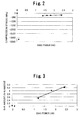
- Fig. 2 is a view showing, in the form of a graph, the experiment result shown in Table 1.
- Table 1 Bias power [kW] 0 0.1 1.4 1.6 1.8 2.4 Compression Stress [Mpa] -44 -3251 -307 -274 -259 -225
- the compression stress is increased by application of the bias power as similar to the conventional case up to the bias power of 0.1 kW (0.1 kW is maximal).
- the compression stress becomes smaller when the bias power is increased further.
- the state of the SiN film was observed in each bias power levels, and it was found out that film detachment occurred at bias power level of 1. 6 kW or lower, but film detachment did not occur at bias power level of 1.8 kW or higher. Accordingly, it is apparent that the bias power needs to be set equal to or higher than a predetermined threshold in order to suppress occurrence of film detachment.
- Table 2 is a table showing the experiment result of the experiment to measure the Si-H bonding amounts and the N-H bonding amounts in the SiN films formed with variation in the bias power to be applied.
- Fig. 3 is a view showing, in the form of a graph, the measurement result of the Si-H amounts/N-H amounts in the SiN films formed with variation in the bias power to be applied, which are shown Table 2.
- the Si-H/N-H is decreased as similar to the conventional case up to the bias power of 0.1 kW.
- the Si-H bonding amount is increased in proportion to the bias power and the Si-H amount/N-H amount are increased.
- Fig. 4 is a view showing a micrograph of the SiN film deposited with a bias power set to 0.5 kW
- Fig. 5 is a view showing a micrograph of the SiN film deposited with a bias power set to 1.6 kW
- Fig. 6 is a view showing the micrograph of a SiN film deposited with a bias power set to 2.4 kW.
- Fig. 4 when the bias power is set to 0.5 kW, film detachment occurs across a front surface of the substrate 21 (see Fig. 1 ). Note that portions which seem like patterns in Fig. 4 represent portions where the film is detached. Meanwhile, as shown in Fig. 5 , when the bias power is set to 1.6 kW, there is minor film detachment. Note that portions which seem like small dots as surrounded by broken lines in Fig. 5 represent portions where the film is detached.
- the film detachment occurs when the bias power is lower than about 1.6 kW, but does not occur when the bias power is about 2.4 kW.
- the compression stress in the SiN film is reduced and the Si-H amount/N-H amount increases when the bias power is set higher than the threshold.
- the bias power (ion impact) lower than the threshold causes enhancement in film density and increase in the compression stress, while the compression stress is reduced due to a drawing effect of hydrogen which occurs when the bias power higher than the threshold is applied.
- the conventional technique has the problem of film detachment due to the increase in the compression stress which occurs when the bias power is increased to embed a SiN film.
- the present invention it has been found out that, by controlling the bias power to be equal to or higher than the threshold, the compression stress is reduced due to the drawing effect of hydrogen. This allows the embedding of a film.
- the bias power (4 MHz) was set to 2.4 kW
- the RF power 13.56 MHz is set to 2 kW
- the flow rates of SiH 4 , N 2 , and Ar were all set to 50 sccm
- the pressure was set to 25 mTorr
- the film deposition temperature is set to 250°C.
- Table 3 is a table showing an experiment result of the experiment to measure the compression stresses of the respective SiN films having the film thicknesses of 350 nm and 10000 nm, respectively.
- Fig. 7 is a view showing, in the form of a graph, the experiment result of the compression stresses in the respective SiN films having different film thicknesses of the SiN film between 350 nm and 10000 nm, respectively, as shown in Table 3.
- the compression stress in the SiN film becomes smaller when the film thickness of the SiN film is increased. This is because the Si-H bonding amount of the entire SiN film increases when the film thickness becomes thicker. Accordingly, the Si-H bonding amount can be controlled by controlling the film thickness, thereby allowing the control of the compression stress in the SiN film.
- the embedding of the film is possible even in a hole having a depth of 1 ⁇ m or more.
- the bias power (4 MHz) was set to 2.4 kW
- the RF power 13.56 MHz was set to 2 kW
- the flow rates of N 2 and Ar were both set to 50 sccm
- the pressure is set to 25 mTorr
- the film deposition temperature was set to 250°C
- the film thickness of the SiN film to be deposited was set to 350 nm.
- Table 4 is a table showing an experiment result of the experiment to measure the compression stresses in the respective SiN films deposited with variation in film deposition rate.
- Fig. 8 is a view showing, in the form of a graph, the experiment result of the compression stresses in the respective SiN films deposited with variation in film deposition rate as shown in Table 4.
- the compression stress in the SiN film becomes larger when the film deposition rate becomes larger. Accordingly, by setting the film deposition rate smaller, it is possible to suppress occurrence of film detachment even when the bias power to be applied is set lower than the above-described threshold of the bias power.
- Table 5 is a table showing an experiment result of the experiment to measure the Si-H bonding amounts in the respective SiN films deposited with variation in film deposition temperature.
- Film deposition 250 430 temperature [C°] Si-H bonding amount 15.8 7.5 [*10 21 /cm 3 ] N-H bonding amount 12.9 10.1 [*10 21 /cm 3 ] Si-H/N-H 1.2 0.74
- the Si-H bonding amount is increased when the film deposition temperature becomes lower. Accordingly, the Si-H bonding amount can be controlled by controlling the film deposition temperature, thereby allowing the control of the compression stress in the SiN film. In other words, the Si-H bonding amount can be increased by lowering the film deposition temperature, thereby allowing reduction of the compression stress in the SiN.
- the bias power (4 MHz) was set to 2.4 kW
- the RF power 13.56 MHz was set to 2 kW
- the flow rate of Ar was set to 50 sccm
- the pressure was set to 25 mTorr
- the film deposition temperature was set to 250°C
- the film thickness of the SiN film to be deposited was set to 350 nm.
- Table 6 is a table showing an experiment result of the experiment to measure the Si-H bonding amounts in the respective SiN films deposited with variation in SiH 4 flow rate/N 2 flow rate.
- SiH 4 flow rate/N 2 flow rate 0.5 1.0 Si-H bonding amount [*10 21 /cm 3 ] 5.1 15.8 N-H bonding amount [*10 21 /cm 3 ] 17.1 12.9 Si-H/N-H 0.3 1.2
- the Si-H bonding amount is increased when the SiH 4 flow rate/N 2 flow rate becomes larger. Accordingly, the Si-H bonding amount can be controlled by controlling the SiH 4 flow rate/N 2 flow rate, thereby allowing the control of the compression stress in the SiN film. In other words, the Si-H bonding amount can be increased by increasing the SiH 4 flow rate/N 2 flow rate, thereby allowing the reduction of the compression stress in the SiN.
- Table 7 is a table showing an experiment result of the experiment to measure the Si-H bonding amounts in the respective SiN films deposited with variation in RF power to be applied.
- RF power [kW] 3.0 4.0 Si-H bonding amount [*10 21 /cm 3 ] 17.1 13.9
- N-H bonding amount [*10 21 /cm 3 ] 6.7 11.4 Si-H/N-H 2.6 1.2
- the Si-H bonding amount is increased when the RF power becomes smaller. Accordingly, the Si-H bonding amount can be controlled by controlling the RF power, thereby allowing the control of the compression stress in the SiN film. In other words, the Si-H bonding amount can be increased by decreasing the RF power, thereby allowing the reduction of the compression stress in the SiN.
- Table 8 is a table showing an experiment result of the experiment to measure the Si-H bonding amounts in the respective SiN films deposited with variation in pressure to be applied.
- Pressure [Pa] 1.3 3.3 Si-H bonding amount [*10 21 /cm 3 ] 8.9 15.8 N-H bonding amount [*10 21 /cm 3 ] 11.1 12.9 Si-H/N-H 0.8 1.2
- the Si-H bonding amount is increased when the pressure becomes higher. Accordingly, the Si-H bonding amount can be controlled by controlling the pressure, thereby allowing the control of the compression stress in the SiN film. In other words, the Si-H bonding amount can be increased by raising the pressure, thereby allowing the reduction of the compression stress in the SiN.
- the Si-H bonding amount in the SiN film can be increased by causing the parameter control device 32 (see Fig. 1 ) to control the bias power, the RF power, the pressure, the film thickness, the gas mixture ratio, and the film deposition temperature, thereby reducing the compression stress in the SiN film. This allows embedding of the SiN film by applying the bias power.
- the process conditions at the time of deposition of the SiN film are set as follows.
- the RF power (13.56 MHz) is 2 kW
- the flow rates of the SiH 4 , N 2 , and Ar are 50 sccm
- the pressure is 25 mTorr
- the film deposition temperature is 250°C
- the film thickness of the SiN film to be deposited is 350 nm.
- This SiN film embedded by applying the bias power can be applied to, for example, an image sensor (CCD/CMOS) lens and a waveguide utilizing a high refractive index and high permeability of the SiN film, a final protective film for wiring utilizing a barrier property of the SiN film.
- an application to the image sensor is effective whose dark current is known to be reduced by terminating dangling-bond of Si atom with hydrogen.
- the present invention is applicable to a plasma processing method capable of embedding SiN film while applying bias power and to a plasma processing system.
Landscapes
- Chemical & Material Sciences (AREA)
- Engineering & Computer Science (AREA)
- Physics & Mathematics (AREA)
- Plasma & Fusion (AREA)
- Metallurgy (AREA)
- Chemical Kinetics & Catalysis (AREA)
- Materials Engineering (AREA)
- Mechanical Engineering (AREA)
- General Chemical & Material Sciences (AREA)
- Organic Chemistry (AREA)
- Analytical Chemistry (AREA)
- Inorganic Chemistry (AREA)
- Chemical Vapour Deposition (AREA)
- Formation Of Insulating Films (AREA)
- Plasma Technology (AREA)
- Internal Circuitry In Semiconductor Integrated Circuit Devices (AREA)
Abstract
Description
- The present invention relates to a plasma processing method and a plasma processing system.
- Needs for embedding a SiN film in a minute hole having a high aspect ratio (such as a hole having a hole diameter φ smaller than 1 µm and an aspect ratio of 1 or more) have been increasing recently along with miniaturization of semiconductor elements. Bias power needs to be increased to perform the embedding of a SiN film by use of a plasma CVD apparatus.
- This is because, when little or no bias power is applied in the film deposition, a film is deposited more at an aperture than at a bottom of the hole due to an incidence angle of a precursor of the film to be deposited. As a result, the aperture of the hole is occluded, and a void is formed inside the hole. However, increasing the bias power causes film deposition and sputtering to be performed at the same time, suppressing the deposition at the aperture and thus allowing the progress of the film deposition at the bottom of and inside the hole. Accordingly, this enables the embedding of a film with no voids. Examples of such plasma processing are disclosed in Non-patent
Document 1 and Non-patentDocument 2 cited below. - Non-patent Document 1: Tatsuru Shirafuji, "Gas phase/surface reactions of plasma-enhanced CVD", [online], [searched on January 16, 2008], the Internet <URL: http://shira.iic.kyoto-u.ac.jp/2006-09-02-PECVD-Lecture.pdf >
- Non-patent Document 2: C. W. Pearce, R. F. Fetcho, M. D. Gross, R. F. Koefer, R. A. Pudliner, "Characteristics of silicon nitride deposited by plasma-enhanced chemical vapor deposition using a dual frequency radio-frequency source" J. Appl. Phys. February 15, 1992, Vol. 71, No. 4, p. 1838-1841
- However, as disclosed in Fig. 31 of the above-mentioned
Non-patent Document 1, in the conventional plasma processing method, the increasing of the bias power causes the (Si-H bonding amount) / (N-H bonding amount) of a SiN film to be reduced, and along therewith, the compression stress increases. Hence there is a problem that occurrence of a detached film attributable to this increase in the compression stress constitutes an obstacle for embedding of a SiN film by applying the bias power. - From this point of view, an object of the present invention is to provide a plasma processing method and a plasma processing system, which are capable of embedding a SiN film while suppressing an increase in compression stress and a decrease in Si-H/N-H bonding due to application of bias power.
- A plasma processing method according to a first invention for solving the above problem is a plasma processing method for depositing a silicon nitride film on a substrate, which is a target for plasma processing, by using plasma of a raw material gas containing silicon and hydrogen and of a gas containing nitrogen, the plasma processing method characterized in that, bias power to inject ions into the substrate is set equal to or higher than a threshold to increase a Si-H bonding amount, thereby reducing compression stress.
- A plasma processing method according to a second invention for solving the above problem is the plasma processing method according to the first invention characterized in that RF power to be applied to generate the plasma is reduced to increase the Si-H bonding amount, thereby reducing the compression stress
- A plasma processing method according to a third invention for solving the above problem is the plasma processing method according to the first invention characterized in that pressure is raised to increase the Si-H bonding amount, thereby reducing the compression stress.
- A plasma processing method according to a fourth invention for solving the above problem is the plasma processing method according to the first invention characterized in that amounts of supply of the gas containing nitrogen are increased to increase the Si-H bonding amount, thereby reducing the compression stress.
- A plasma processing method according to a fifth invention for solving the above problem is the plasma processing method according to the first invention characterized in that a plasma processing temperature is lowered to increase the Si-H bonding amount, thereby reducing the compression stress.
- A plasma processing method according to a sixth invention for solving the above problem is the plasma processing method according to the first invention characterized in that the threshold is set to 1.2 kW in a case of a 200-mm wafer.
- A plasma processing system according to a seventh invention for solving the above problem is a plasma processing system characterized by comprising: gas supply amount controlling means for controlling gas supply amounts of a raw material gas containing silicon and hydrogen and a gas containing nitrogen to be supplied into a vacuum chamber; pressure controlling means for controlling pressure inside the vacuum chamber; plasma generating means for generating plasma by applying RF power to the raw material gas and the nitrogen gas inside the vacuum chamber; substrate holding means for holding a substrate, which is a target for plasma processing, inside the vacuum chamber; temperature controlling means for controlling a temperature during the plasma processing of the substrate; bias power applying means for applying bias power to the substrate; and parameter controlling means for setting the bias power to inject ions into the substrate equal to or higher than a threshold to increase a Si-H bonding amount, thereby reducing compression stress.
- According to the present invention, in a plasma processing method of depositing a silicon nitride film on a substrate, which is a target for plasma processing, by using plasma of a raw material gas containing silicon and hydrogen and a gas containing nitrogen, compression stress in the silicon nitride film can be reduced by increasing a Si-H bonding amount in the silicon nitride film. This suppresses film detachment attributable to an increase of the compression stress in the SiN film at the time of bias power application. Therefore, it is possible to embed a SiN film by applying the bias power.
-
- [
Fig. 1] Fig. 1 is a configuration diagram of a plasma processing system according to an embodiment of the present invention. - [
Fig. 2] Fig. 2 is a view showing, in the form of a graph, an experiment result of an experiment to measure compression stresses in respective SiN films formed with variation in the bias power to be applied. - [
Fig. 3] Fig. 3 is a view showing, in the form of a graph, an experiment result of an experiment to measure Si-H amount/N-H amount in respective SiN films formed with variation in the bias power to be applied. - [
Fig. 4] Fig. 4 is a view showing a micrograph of the SiN film deposited with a bias power set to 0.5 kW. - [
Fig. 5] Fig. 5 is a view showing a micrograph of the SiN film deposited with a bias power set to 1.6 kW. - [
Fig. 6] Fig. 6 is a view showing a micrograph of the SiN film deposited with a bias power set to 2.4 kW. - [
Fig. 7] Fig. 7 is a view showing, in the form of a graph, an experiment result of an experiment to measure compression stresses in respective SiN films having a different film thicknesses. - [
Fig. 8] Fig. 8 is a view showing, in the form of a graph, an experiment result of an experiment to measure compression stresses in respective SiN films deposited with variation in film deposition rate. - An embodiment of a plasma processing method and a plasma processing system according to the present invention will be described below by using the drawings.
Fig. 1 is a configuration diagram of the plasma processing system according to the embodiment of the present invention. As shown inFig. 1 , theplasma processing system 1 includes avacuum chamber 10 capable of maintaining a high degree of vacuum. Thisvacuum chamber 10 includes acylindrical container 11 and aceiling plate 12 and forms a space which is hermetically sealed from outside air by fitting theceiling plate 12 onto an upper portion of thecylindrical container 11. - The
vacuum chamber 10 is provided with avacuum device 13 to establish a vacuum state inside thevacuum chamber 10. ARF antenna 15 configured to generateplasma 14 is located at an upper portion of theceiling plate 12. ARF power source 17 being a high-frequency power source is connected to thisRF antenna 15 via arectifier 16. Specifically, RF power supplied from theRF power source 17 is supplied to theplasma 14 through theRF antenna 15. - A raw material
gas supply tube 18 configured to supply raw material gas being a material of a film to be deposited into thevacuum chamber 10 is disposed at an upper portion of a side wall of thecylindrical container 11. The raw materialgas supply tube 18 is provided with a raw material gas supplyamount control valve 18a configured to control a supply amount of the raw material gas. In this embodiment, SiH4 is supplied as the raw material gas. A N2gas supply tube 19 configured to supply N2 gas into thevacuum chamber 10 is disposed at the upper portion of the side wall of thecylindrical container 11. The N2gas supply tube 19 is provided with a N2 gas supplyamount control valve 19a configured to control a supply amount of the N2 gas. An Arsupply tube 20 configured to supply Ar gas into thevacuum chamber 10 is disposed at the upper portion of the side wall of thecylindrical container 11. The Argas supply tube 20 is provided with an Ar gas supplyamount control valve 20a configured to control a supply amount of the Ar gas. By these constituents, theplasma 14 of SiH4, N2, and Ar is generated in an upper portion inside thevacuum chamber 10. - A substrate support table 22 configured to hold a
substrate 21 being a target for film deposition is disposed in a lower portion inside thecylindrical container 11. This substrate support table 22 includes asubstrate holding portion 23 configured to hold thesubstrate 21 and asupport shaft 24 configured to support thissubstrate holding portion 23. Aheater 25 for heating is disposed inside thesubstrate holding portion 23. Aheater control device 26 adjusts the temperature of thisheater 25. Accordingly, it is possible to control the temperature of thesubstrate 21 during the plasma processing. - A
bias power source 29 is connected to thesubstrate holding portion 23 via a capacitor 27 and arectifier 28 so that bias power can be applied to thesubstrate 21. This makes it possible to draw ions from theplasma 14 to a surface of thesubstrate 21. Further, anelectrostatic power source 30 is connected to thesubstrate holding portion 23 so that thesubstrate 21 can be held by an electrostatic force. Theelectrostatic power source 30 is connected to thesubstrate holding portion 22 via a low-pass filter 31 (LPF) so that power from theRF power source 17 and thebias power source 29 does not flow into theelectrostatic power source 30. - Additionally, a parameter control device 32 is provided which is capable of controlling the bias power of the
bias power source 29, the RF power of theRF power source 17, pressure of thevacuum device 13, theheater control device 26, and the gas supply amounts of the raw materialgas supply valve 18a, the N2gas supply valve 19a, and the Argas supply valve 20a, respectively. Note that dashed lines inFig. 1 represent signal lines for transmitting control signals from the parameter control device to thebias power source 29, theRF power source 17, thevacuum device 13, theheater control device 26, the raw materialgas supply valve 18a, the N2gas supply valve 19a, and the Argas supply valve 20a. - In the above-described plasma processing system according to this embodiment, embedding of a film by applying the bias power is made possible by use of the parameter control device 32 which controls the bias power, the RF power, the pressure, a film deposition temperature, and the gas supply amounts on the basis of conditions to be described later. The parameter control device 32 according to this embodiment particularly sets the bias power for injecting ions into the
substrate 21 equal to or higher than a threshold to increase a Si-H bonding amount, thereby performing control to reduce compression stress. Here, the reason why it is possible to reduce the compression stress by setting the bias power for injecting ions into thesubstrate 21 equal to or higher than the threshold to increase the Si-H bonding amount will be described below in detail. - Now, experiment results of various experiments carried out by using the plasma processing system according to this embodiment will be described to begin with.
An experiment was performed as a first experiment in which compression stresses, a Si-H bonding amounts, and a N-H bonding amounts in respective SiN films were measured, the SiN films each applied with different bias power while being formed. Here, the substrate 21 (seeFig. 1 ) as the target for film deposition processing is assumed to be a wafer having a diameter of 200 mm. As for process conditions at the time of deposition of each of the SiN films, the RF power (13.56 MHz) was set to 2 kW, flow rates of SiH4, N2, and Ar were all set to 50 sccm, the pressure was set to 25 mTorr, the film deposition temperature was set to 250°C, and a film thickness of the SiN film to be deposited was set to 350 nm. - Shown are results of measurement of compression stresses in the respective SiN films formed under the above-described process conditions with variation in the bias power (4 MHz) to be applied. Table 1 is a table showing the experiment result of the experiment to measure the compression stresses in the respective SiN films formed with variation in the bias power to be applied.
Fig. 2 is a view showing, in the form of a graph, the experiment result shown in Table 1.[Table 1] Bias power [kW] 0 0.1 1.4 1.6 1.8 2.4 Compression Stress [Mpa] -44 -3251 -307 -274 -259 -225 - As shown in
Fig. 2 , the compression stress is increased by application of the bias power as similar to the conventional case up to the bias power of 0.1 kW (0.1 kW is maximal). However, the compression stress becomes smaller when the bias power is increased further. Moreover, the state of the SiN film was observed in each bias power levels, and it was found out that film detachment occurred at bias power level of 1. 6 kW or lower, but film detachment did not occur at bias power level of 1.8 kW or higher. Accordingly, it is apparent that the bias power needs to be set equal to or higher than a predetermined threshold in order to suppress occurrence of film detachment. For this reason, it is necessary to apply the bias power of 5.7 W/cm2 per unit area (1.8 kW in the case of the 200-mm wafer) or higher to the substrate 21 (seeFig. 1 ) in order to set the bias power equal to or higher than the threshold. - Shown is a result of measurement of the Si-H bonding amounts and the N-H bonding amounts of the SiN films formed under the above-described process conditions with variation in the bias power (4 MHz) to be applied, the measurement performed by using a FTIR (Fourier transform infrared spectrophotometer). Table 2 is a table showing the experiment result of the experiment to measure the Si-H bonding amounts and the N-H bonding amounts in the SiN films formed with variation in the bias power to be applied. Meanwhile,
Fig. 3 is a view showing, in the form of a graph, the measurement result of the Si-H amounts/N-H amounts in the SiN films formed with variation in the bias power to be applied, which are shown Table 2.[Table 2] Bias power [kW] 0 0.1 1.2 1.8 2.4 Si-H bonding amount 0.9 0.78 5.7 12.2 15.8 [*1021/cm3] N-H bonding amount 19.5 31 11.0 12.0 12.9 [*1021/cm3] Si-H/N-H 0.05 0.025 0.52 1.0 1.2 - As shown in
Fig. 3 , the Si-H/N-H is decreased as similar to the conventional case up to the bias power of 0.1 kW. However, when the bias power is increased further, the Si-H bonding amount is increased in proportion to the bias power and the Si-H amount/N-H amount are increased. - The state of each of the deposited SiN films in the case where the bias power is set to 0.5kW, 1.6 kW, or 2.4 kW during the deposition of the SiN film will be described.
Fig. 4 is a view showing a micrograph of the SiN film deposited with a bias power set to 0.5 kW,Fig. 5 is a view showing a micrograph of the SiN film deposited with a bias power set to 1.6 kW, andFig. 6 is a view showing the micrograph of a SiN film deposited with a bias power set to 2.4 kW. - As shown in
Fig. 4 , when the bias power is set to 0.5 kW, film detachment occurs across a front surface of the substrate 21 (seeFig. 1 ). Note that portions which seem like patterns inFig. 4 represent portions where the film is detached. Meanwhile, as shown inFig. 5 , when the bias power is set to 1.6 kW, there is minor film detachment. Note that portions which seem like small dots as surrounded by broken lines inFig. 5 represent portions where the film is detached. - Meanwhile, as shown in
Fig. 6 , when the bias power is set to 2.4 kW, film detachment does not occur. Accordingly, the film detachment occurs when the bias power is lower than about 1.6 kW, but does not occur when the bias power is about 2.4 kW. - From the result of the first experiment, the compression stress in the SiN film is reduced and the Si-H amount/N-H amount increases when the bias power is set higher than the threshold. This is presumably because the bias power (ion impact) lower than the threshold causes enhancement in film density and increase in the compression stress, while the compression stress is reduced due to a drawing effect of hydrogen which occurs when the bias power higher than the threshold is applied. In other words, the conventional technique has the problem of film detachment due to the increase in the compression stress which occurs when the bias power is increased to embed a SiN film. Meanwhile, in the present invention, it has been found out that, by controlling the bias power to be equal to or higher than the threshold, the compression stress is reduced due to the drawing effect of hydrogen. This allows the embedding of a film.
- An experiment was performed as a second experiment in which the compression stresses were measured in respective cases where the film thicknesses of the SiN film to be deposited were 350 nm and 10000 nm, respectively, at the time of deposition of the SiN films. Here, the substrate 21 (see
Fig. 1 ) as the target for film deposition processing is assumed to be a wafer having the diameter of 200 mm. As for process conditions at the time of deposition of each of the SiN films, the bias power (4 MHz) was set to 2.4 kW, the RF power (13.56 MHz) is set to 2 kW, the flow rates of SiH4, N2, and Ar were all set to 50 sccm, the pressure was set to 25 mTorr, and the film deposition temperature is set to 250°C. - Table 3 is a table showing an experiment result of the experiment to measure the compression stresses of the respective SiN films having the film thicknesses of 350 nm and 10000 nm, respectively. Meanwhile,
Fig. 7 is a view showing, in the form of a graph, the experiment result of the compression stresses in the respective SiN films having different film thicknesses of the SiN film between 350 nm and 10000 nm, respectively, as shown in Table 3.[Table 3] Film thickness [nm] 350 10000 Compression stress [MPa] -225 -164 - As shown in
Fig. 7 , the compression stress in the SiN film becomes smaller when the film thickness of the SiN film is increased. This is because the Si-H bonding amount of the entire SiN film increases when the film thickness becomes thicker. Accordingly, the Si-H bonding amount can be controlled by controlling the film thickness, thereby allowing the control of the compression stress in the SiN film. Here, it turns out from the result of the second experiment that the embedding of the film is possible even in a hole having a depth of 1 µm or more. - An experiment was performed as a third experiment in which the compression stresses in the respective SiN films were measured, the SiN films deposited with variation in film deposition rate by changing the flow rate of SiH4 at the time of deposition of the SiN film. Here, the substrate 21 (see
Fig. 1 ) as the target for film deposition processing is assumed to be a wafer having the diameter of 200 mm. As for process conditions at the time of deposition of each of the SiN films, the bias power (4 MHz) was set to 2.4 kW, the RF power (13.56 MHz) was set to 2 kW, the flow rates of N2 and Ar were both set to 50 sccm, the pressure is set to 25 mTorr, the film deposition temperature was set to 250°C, and the film thickness of the SiN film to be deposited was set to 350 nm. - Table 4 is a table showing an experiment result of the experiment to measure the compression stresses in the respective SiN films deposited with variation in film deposition rate. Meanwhile,
Fig. 8 is a view showing, in the form of a graph, the experiment result of the compression stresses in the respective SiN films deposited with variation in film deposition rate as shown in Table 4.[Table 4] SiH4 flow rate [sccm] 50 80 150 Film deposition rate [nm/sec] 1.6 3.7 8.8 Compression stress [MPa] -225 -408 -642 - As shown in
Fig. 8 , the compression stress in the SiN film becomes larger when the film deposition rate becomes larger. Accordingly, by setting the film deposition rate smaller, it is possible to suppress occurrence of film detachment even when the bias power to be applied is set lower than the above-described threshold of the bias power. - An experiment was performed as a fourth experiment in which the Si-H bonding amounts in the respective SiN films were measured, the SiN films deposited with variation in film deposition temperature. Here, the substrate 21 (see
Fig. 1 ) as the target for film deposition processing is assumed to be a wafer having the diameter of 200 mm. As for process conditions at the time of deposition of each of the SiN films, the bias power (4 MHz) was set to 2.4 kW, the RF power (13.56 MHz) was set to 2 kW, the flow rates of SiH4, N2, and Ar were all set to 50 sccm, the pressure was set to 25 mTorr, and the film thickness of the SiN film to be deposited was set to 350 nm. - Table 5 is a table showing an experiment result of the experiment to measure the Si-H bonding amounts in the respective SiN films deposited with variation in film deposition temperature.
[Table 5] Film deposition 250 430 temperature [C°] Si-H bonding amount 15.8 7.5 [*1021/cm3] N-H bonding amount 12.9 10.1 [*1021/cm3] Si-H/N-H 1.2 0.74 - As shown in Table 5, the Si-H bonding amount is increased when the film deposition temperature becomes lower. Accordingly, the Si-H bonding amount can be controlled by controlling the film deposition temperature, thereby allowing the control of the compression stress in the SiN film. In other words, the Si-H bonding amount can be increased by lowering the film deposition temperature, thereby allowing reduction of the compression stress in the SiN.
- An experiment was performed as a fifth experiment in which the Si-H bonding amounts in the respective SiN films were measured, the SiN films deposited with variation in flow rate of SiH4 relative to the flow rate of N2 (the SiH4 flow rate/N2 flow rate) . Here, the substrate 21 (see
Fig. 1 ) as the target for film deposition processing is assumed to be a wafer having the diameter of 200 mm. As for process conditions at the time of deposition of each of the SiN films, the bias power (4 MHz) was set to 2.4 kW, the RF power (13.56 MHz) was set to 2 kW, the flow rate of Ar was set to 50 sccm, the pressure was set to 25 mTorr, the film deposition temperature was set to 250°C, and the film thickness of the SiN film to be deposited was set to 350 nm. - Table 6 is a table showing an experiment result of the experiment to measure the Si-H bonding amounts in the respective SiN films deposited with variation in SiH4 flow rate/N2 flow rate.
[Table 6] SiH4 flow rate/N2 flow rate 0.5 1.0 Si-H bonding amount [*1021/cm3] 5.1 15.8 N-H bonding amount [*1021/cm3] 17.1 12.9 Si-H/N-H 0.3 1.2 - As shown in Table 6, the Si-H bonding amount is increased when the SiH4 flow rate/N2 flow rate becomes larger. Accordingly, the Si-H bonding amount can be controlled by controlling the SiH4 flow rate/N2 flow rate, thereby allowing the control of the compression stress in the SiN film. In other words, the Si-H bonding amount can be increased by increasing the SiH4 flow rate/N2 flow rate, thereby allowing the reduction of the compression stress in the SiN.
- An experiment was performed as a sixth experiment in which the Si-H bonding amounts in SiN films deposited with variation in RF power to be applied. Here, the substrate 21 (see
Fig. 1 ) as the target for film deposition processing is assumed to be a wafer having the diameter of 200 mm. As for process conditions at the time of deposition of each of the SiN films, the bias power (4 MHz) was set to 2.4 kW, the flow rates of SiH4, N2, and Ar were all set to 50 sccm, the pressure was set to 25 mTorr, the film deposition temperature was set to 250°C, and the film thickness of the SiN film to be deposited was set to 350 nm. - Table 7 is a table showing an experiment result of the experiment to measure the Si-H bonding amounts in the respective SiN films deposited with variation in RF power to be applied.
[Table 7] RF power [kW] 3.0 4.0 Si-H bonding amount [*1021/cm3] 17.1 13.9 N-H bonding amount [*1021/cm3] 6.7 11.4 Si-H/N-H 2.6 1.2 - As shown in Table 7, the Si-H bonding amount is increased when the RF power becomes smaller. Accordingly, the Si-H bonding amount can be controlled by controlling the RF power, thereby allowing the control of the compression stress in the SiN film. In other words, the Si-H bonding amount can be increased by decreasing the RF power, thereby allowing the reduction of the compression stress in the SiN.
- An experiment was performed as a seventh experiment in which the Si-H bonding amounts in SiN films were measured, the SiN films deposited with variation in pressure to be applied. Here, the substrate 21 (see
Fig. 1 ) as the target for film deposition processing is assumed to be a wafer having the diameter of 200 mm. As for process conditions at the time of deposition of each of the SiN films, the bias power (4 MHz) was set to 2.4 kW, the RF power (13.56 MHz) was set to 2 kW, the flow rates of SiH4, N2, and Ar were all set to 50 sccm, the film deposition temperature was set to 250°C, and the film thickness of the SiN film to be deposited was set to 350 nm. - Table 8 is a table showing an experiment result of the experiment to measure the Si-H bonding amounts in the respective SiN films deposited with variation in pressure to be applied.
[Table 8] Pressure [Pa] 1.3 3.3 Si-H bonding amount [*1021/cm3] 8.9 15.8 N-H bonding amount [*1021/cm3] 11.1 12.9 Si-H/N-H 0.8 1.2 - As shown in Table 8, the Si-H bonding amount is increased when the pressure becomes higher. Accordingly, the Si-H bonding amount can be controlled by controlling the pressure, thereby allowing the control of the compression stress in the SiN film. In other words, the Si-H bonding amount can be increased by raising the pressure, thereby allowing the reduction of the compression stress in the SiN.
- As described above, from the results of the first to seventh experiments, it is found out that there is a negative correlation between the amount of Si-H groups (the Si-H bonding amount) in the SiN film and the compression stress in the SiN film in an area applied with the bias power equal to or higher than the threshold. Accordingly, the Si-H bonding amount in the SiN film can be increased by causing the parameter control device 32 (see
Fig. 1 ) to control the bias power, the RF power, the pressure, the film thickness, the gas mixture ratio, and the film deposition temperature, thereby reducing the compression stress in the SiN film. This allows embedding of the SiN film by applying the bias power. - To be more precise, assume that the process conditions at the time of deposition of the SiN film are set as follows. The RF power (13.56 MHz) is 2 kW, the flow rates of the SiH4, N2, and Ar are 50 sccm, the pressure is 25 mTorr, the film deposition temperature is 250°C, and the film thickness of the SiN film to be deposited is 350 nm. Here, the parameter control device 32 performs a control so that the bias power of 5.7 W/cm2 per unit area or higher (in the case of the 200-mm wafer, the radius r of the wafer = 10 cm and the area of the wafer is πr2= 3.14 × 102 cm2= 314 cm2; therefore, the bias power to be applied to the wafer is 314 cm2 × 5.7 W/cm2 = 1.79 kW, and this value is rounded to the nearest tenth above to 1.8 kW) is applied to the substrate 21 (see
Fig. 1 ) as the target for film deposition. Moreover, when the bias power of 5.7 W/cm2 per unit area or lower is applied to the substrate 21 (seeFig. 1 ) as the target for film deposition, the control is performed so that the RF power becomes smaller, the pressure becomes higher, the SiH4 flow rate/N2 flow rate becomes larger, and the film deposition temperature becomes lower. - This SiN film embedded by applying the bias power can be applied to, for example, an image sensor (CCD/CMOS) lens and a waveguide utilizing a high refractive index and high permeability of the SiN film, a final protective film for wiring utilizing a barrier property of the SiN film. In particular, since it is possible to increase the Si-H bonding amount in the film by controlling the bias power, the RF power, the pressure, the film thickness, the gas mixture ratio, and the film deposition temperature, an application to the image sensor is effective whose dark current is known to be reduced by terminating dangling-bond of Si atom with hydrogen.
- The present invention is applicable to a plasma processing method capable of embedding SiN film while applying bias power and to a plasma processing system.
Claims (7)
- A plasma processing method for depositing a silicon nitride film on a substrate, which is a target for plasma processing, by using plasma of a raw material gas containing silicon and hydrogen and of a gas containing nitrogen, the plasma processing method characterized in that,
bias power to inject ions into the substrate is set equal to or higher than a threshold to increase a Si-H bonding amount, thereby reducing compression stress. - The plasma processing method according to claim 1, characterized in that RF power to be applied to generate the plasma is reduced to increase the Si-H bonding amount, thereby reducing the compression stress.
- The plasma processing method according to claim 1, characterized in that pressure is raised to increase the Si-H bonding amount, thereby reducing the compression stress.
- The plasma processing method according to claim 1, characterized in that amounts of supply of the raw material gas and the gas containing nitrogen are increased to increase the Si-H bonding amount, thereby reducing the compression stress.
- The plasma processing method according to claim 1, characterized in that a plasma processing temperature is lowered to increase the Si-H bonding amount, thereby reducing the compression stress.
- The plasma processing method according to claim 1, characterized in that the threshold is set to 1.2 kW in a case of a 200-mm wafer.
- A plasma processing system characterized by comprising:gas supply amount controlling means for controlling gas supply amounts of a raw material gas containing silicon and hydrogen and a gas containing nitrogen to be supplied into a vacuum chamber;pressure controlling means for controlling pressure inside the vacuum chamber;plasma generating means for generating plasma by applying RF power to the raw material gas and the nitrogen gas inside the vacuum chamber;substrate holding means for holding a substrate, which is a target for plasma processing, inside the vacuum chamber;temperature controlling means for controlling a temperature during the plasma processing of the substrate;bias power applying means for applying bias power to the substrate; andparameter controlling means for setting the bias power to inject ions into the substrate equal to or higher than a threshold to increase a Si-H bonding amount, thereby reducing compression stress.
Applications Claiming Priority (2)
| Application Number | Priority Date | Filing Date | Title |
|---|---|---|---|
| JP2008015894A JP5297048B2 (en) | 2008-01-28 | 2008-01-28 | Plasma processing method and plasma processing apparatus |
| PCT/JP2009/050703 WO2009096259A1 (en) | 2008-01-28 | 2009-01-20 | Plasma processing method and plasma processing system |
Publications (2)
| Publication Number | Publication Date |
|---|---|
| EP2242092A1 true EP2242092A1 (en) | 2010-10-20 |
| EP2242092A4 EP2242092A4 (en) | 2014-02-05 |
Family
ID=40912612
Family Applications (1)
| Application Number | Title | Priority Date | Filing Date |
|---|---|---|---|
| EP09705243.5A Withdrawn EP2242092A4 (en) | 2008-01-28 | 2009-01-20 | PLASMA PROCESSING METHOD AND PLASMA PROCESSING SYSTEM |
Country Status (6)
| Country | Link |
|---|---|
| US (2) | US20100310791A1 (en) |
| EP (1) | EP2242092A4 (en) |
| JP (1) | JP5297048B2 (en) |
| KR (1) | KR101158377B1 (en) |
| TW (1) | TW200947551A (en) |
| WO (1) | WO2009096259A1 (en) |
Cited By (3)
| Publication number | Priority date | Publication date | Assignee | Title |
|---|---|---|---|---|
| EP2573803A4 (en) * | 2010-05-21 | 2013-12-18 | Mitsubishi Heavy Ind Ltd | SILICON NITRIDE LAYER FOR SEMICONDUCTOR ELEMENT AND METHOD AND APPARATUS FOR MANUFACTURING SILICON NITRIDE LAYER |
| EP2579300A4 (en) * | 2010-05-28 | 2013-12-18 | Mitsubishi Heavy Ind Ltd | SEMICONDUCTOR ELEMENT SILICON NITRIDE FILM, AND METHOD AND DEVICE FOR MANUFACTURING SILICON NITRIDE FILM |
| EP2579301A4 (en) * | 2010-05-28 | 2013-12-18 | Mitsubishi Heavy Ind Ltd | APPARATUS AND METHOD FOR PRODUCING SILICON NITRIDE FILM |
Families Citing this family (51)
| Publication number | Priority date | Publication date | Assignee | Title |
|---|---|---|---|---|
| JP5069597B2 (en) * | 2008-03-27 | 2012-11-07 | 富士フイルム株式会社 | Method for producing gas barrier film |
| US9076646B2 (en) | 2010-04-15 | 2015-07-07 | Lam Research Corporation | Plasma enhanced atomic layer deposition with pulsed plasma exposure |
| US9997357B2 (en) | 2010-04-15 | 2018-06-12 | Lam Research Corporation | Capped ALD films for doping fin-shaped channel regions of 3-D IC transistors |
| US9390909B2 (en) | 2013-11-07 | 2016-07-12 | Novellus Systems, Inc. | Soft landing nanolaminates for advanced patterning |
| US8956983B2 (en) | 2010-04-15 | 2015-02-17 | Novellus Systems, Inc. | Conformal doping via plasma activated atomic layer deposition and conformal film deposition |
| US8637411B2 (en) | 2010-04-15 | 2014-01-28 | Novellus Systems, Inc. | Plasma activated conformal dielectric film deposition |
| US9611544B2 (en) | 2010-04-15 | 2017-04-04 | Novellus Systems, Inc. | Plasma activated conformal dielectric film deposition |
| US20110256734A1 (en) | 2010-04-15 | 2011-10-20 | Hausmann Dennis M | Silicon nitride films and methods |
| US9373500B2 (en) | 2014-02-21 | 2016-06-21 | Lam Research Corporation | Plasma assisted atomic layer deposition titanium oxide for conformal encapsulation and gapfill applications |
| US9892917B2 (en) | 2010-04-15 | 2018-02-13 | Lam Research Corporation | Plasma assisted atomic layer deposition of multi-layer films for patterning applications |
| US9257274B2 (en) | 2010-04-15 | 2016-02-09 | Lam Research Corporation | Gapfill of variable aspect ratio features with a composite PEALD and PECVD method |
| US9685320B2 (en) | 2010-09-23 | 2017-06-20 | Lam Research Corporation | Methods for depositing silicon oxide |
| US8844793B2 (en) * | 2010-11-05 | 2014-09-30 | Raytheon Company | Reducing formation of oxide on solder |
| US8592328B2 (en) * | 2012-01-20 | 2013-11-26 | Novellus Systems, Inc. | Method for depositing a chlorine-free conformal sin film |
| US20140038421A1 (en) * | 2012-08-01 | 2014-02-06 | Taiwan Semiconductor Manufacturing Company, Ltd. | Deposition Chamber and Injector |
| JP2014060378A (en) * | 2012-08-23 | 2014-04-03 | Tokyo Electron Ltd | Silicon nitride film deposition method, organic electronic device manufacturing method and silicon nitride film deposition device |
| US9355839B2 (en) | 2012-10-23 | 2016-05-31 | Lam Research Corporation | Sub-saturated atomic layer deposition and conformal film deposition |
| SG2013083654A (en) | 2012-11-08 | 2014-06-27 | Novellus Systems Inc | Methods for depositing films on sensitive substrates |
| SG2013083241A (en) | 2012-11-08 | 2014-06-27 | Novellus Systems Inc | Conformal film deposition for gapfill |
| US9214334B2 (en) | 2014-02-18 | 2015-12-15 | Lam Research Corporation | High growth rate process for conformal aluminum nitride |
| US9478411B2 (en) | 2014-08-20 | 2016-10-25 | Lam Research Corporation | Method to tune TiOx stoichiometry using atomic layer deposited Ti film to minimize contact resistance for TiOx/Ti based MIS contact scheme for CMOS |
| US9478438B2 (en) | 2014-08-20 | 2016-10-25 | Lam Research Corporation | Method and apparatus to deposit pure titanium thin film at low temperature using titanium tetraiodide precursor |
| US9214333B1 (en) | 2014-09-24 | 2015-12-15 | Lam Research Corporation | Methods and apparatuses for uniform reduction of the in-feature wet etch rate of a silicon nitride film formed by ALD |
| US9589790B2 (en) | 2014-11-24 | 2017-03-07 | Lam Research Corporation | Method of depositing ammonia free and chlorine free conformal silicon nitride film |
| US9564312B2 (en) | 2014-11-24 | 2017-02-07 | Lam Research Corporation | Selective inhibition in atomic layer deposition of silicon-containing films |
| US10566187B2 (en) | 2015-03-20 | 2020-02-18 | Lam Research Corporation | Ultrathin atomic layer deposition film accuracy thickness control |
| US9502238B2 (en) | 2015-04-03 | 2016-11-22 | Lam Research Corporation | Deposition of conformal films by atomic layer deposition and atomic layer etch |
| US10526701B2 (en) | 2015-07-09 | 2020-01-07 | Lam Research Corporation | Multi-cycle ALD process for film uniformity and thickness profile modulation |
| US9601693B1 (en) | 2015-09-24 | 2017-03-21 | Lam Research Corporation | Method for encapsulating a chalcogenide material |
| US9773643B1 (en) | 2016-06-30 | 2017-09-26 | Lam Research Corporation | Apparatus and method for deposition and etch in gap fill |
| US10062563B2 (en) | 2016-07-01 | 2018-08-28 | Lam Research Corporation | Selective atomic layer deposition with post-dose treatment |
| CN107665800B (en) * | 2016-07-28 | 2019-06-07 | 中微半导体设备(上海)股份有限公司 | A kind of radio-frequency power supply control device and its control method for plasma processor |
| US10629435B2 (en) | 2016-07-29 | 2020-04-21 | Lam Research Corporation | Doped ALD films for semiconductor patterning applications |
| US10037884B2 (en) | 2016-08-31 | 2018-07-31 | Lam Research Corporation | Selective atomic layer deposition for gapfill using sacrificial underlayer |
| US10074543B2 (en) | 2016-08-31 | 2018-09-11 | Lam Research Corporation | High dry etch rate materials for semiconductor patterning applications |
| US9865455B1 (en) | 2016-09-07 | 2018-01-09 | Lam Research Corporation | Nitride film formed by plasma-enhanced and thermal atomic layer deposition process |
| US10454029B2 (en) | 2016-11-11 | 2019-10-22 | Lam Research Corporation | Method for reducing the wet etch rate of a sin film without damaging the underlying substrate |
| US10832908B2 (en) | 2016-11-11 | 2020-11-10 | Lam Research Corporation | Self-aligned multi-patterning process flow with ALD gapfill spacer mask |
| US10134579B2 (en) | 2016-11-14 | 2018-11-20 | Lam Research Corporation | Method for high modulus ALD SiO2 spacer |
| US10269559B2 (en) | 2017-09-13 | 2019-04-23 | Lam Research Corporation | Dielectric gapfill of high aspect ratio features utilizing a sacrificial etch cap layer |
| US11404275B2 (en) | 2018-03-02 | 2022-08-02 | Lam Research Corporation | Selective deposition using hydrolysis |
| WO2020222853A1 (en) | 2019-05-01 | 2020-11-05 | Lam Research Corporation | Modulated atomic layer deposition |
| JP7546000B2 (en) | 2019-06-04 | 2024-09-05 | ラム リサーチ コーポレーション | Polymeric protective layers for reactive ion etching in patterning. |
| CN114245832B (en) | 2019-06-07 | 2025-10-28 | 朗姆研究公司 | In-situ control of film properties during atomic layer deposition |
| WO2021025874A1 (en) | 2019-08-06 | 2021-02-11 | Lam Research Corporation | Thermal atomic layer deposition of silicon-containing films |
| JP7240517B2 (en) * | 2019-09-20 | 2023-03-15 | 株式会社Kokusai Electric | Semiconductor device manufacturing method, substrate processing method, program, and substrate processing apparatus |
| WO2022020528A1 (en) | 2020-07-23 | 2022-01-27 | Lam Research Corporation | Conformal thermal cvd with controlled film properties and high deposition rate |
| KR20230043795A (en) | 2020-07-28 | 2023-03-31 | 램 리써치 코포레이션 | Impurity Reduction in Silicon-Containing Films |
| JP2022080674A (en) | 2020-11-18 | 2022-05-30 | 東京エレクトロン株式会社 | Plasma processing apparatus |
| US12473633B2 (en) | 2021-07-09 | 2025-11-18 | Lam Research Corporation | Plasma enhanced atomic layer deposition of silicon-containing films |
| US20240110284A1 (en) * | 2022-09-30 | 2024-04-04 | Applied Materials, Inc. | Selective Deposition of Thin Films with Improved Stability |
Family Cites Families (50)
| Publication number | Priority date | Publication date | Assignee | Title |
|---|---|---|---|---|
| US6068784A (en) * | 1989-10-03 | 2000-05-30 | Applied Materials, Inc. | Process used in an RF coupled plasma reactor |
| JPH04297033A (en) * | 1990-05-28 | 1992-10-21 | Fuji Electric Co Ltd | Formation of silicon nitride film |
| US6090303A (en) * | 1991-06-27 | 2000-07-18 | Applied Materials, Inc. | Process for etching oxides in an electromagnetically coupled planar plasma apparatus |
| US6024826A (en) * | 1996-05-13 | 2000-02-15 | Applied Materials, Inc. | Plasma reactor with heated source of a polymer-hardening precursor material |
| KR100281345B1 (en) * | 1992-12-01 | 2001-03-02 | 조셉 제이. 스위니 | Oxide Etching Process in Electromagnetically Coupled Planner Plasma Device |
| US5571366A (en) * | 1993-10-20 | 1996-11-05 | Tokyo Electron Limited | Plasma processing apparatus |
| US5777289A (en) * | 1995-02-15 | 1998-07-07 | Applied Materials, Inc. | RF plasma reactor with hybrid conductor and multi-radius dome ceiling |
| JPH08115912A (en) * | 1994-10-14 | 1996-05-07 | Nippon Telegr & Teleph Corp <Ntt> | Method for producing silicon nitride thin film |
| US6270617B1 (en) * | 1995-02-15 | 2001-08-07 | Applied Materials, Inc. | RF plasma reactor with hybrid conductor and multi-radius dome ceiling |
| JPH0982495A (en) * | 1995-09-18 | 1997-03-28 | Toshiba Corp | Plasma generating apparatus and plasma generating method |
| JPH09106899A (en) * | 1995-10-11 | 1997-04-22 | Anelva Corp | Plasma CVD apparatus and method and dry etching apparatus and method |
| EP0777258A3 (en) * | 1995-11-29 | 1997-09-17 | Applied Materials Inc | Self-cleaning plasma reactor |
| US5965034A (en) * | 1995-12-04 | 1999-10-12 | Mc Electronics Co., Ltd. | High frequency plasma process wherein the plasma is executed by an inductive structure in which the phase and anti-phase portion of the capacitive currents between the inductive structure and the plasma are balanced |
| US6902683B1 (en) * | 1996-03-01 | 2005-06-07 | Hitachi, Ltd. | Plasma processing apparatus and plasma processing method |
| US5683548A (en) * | 1996-02-22 | 1997-11-04 | Motorola, Inc. | Inductively coupled plasma reactor and process |
| TW335517B (en) * | 1996-03-01 | 1998-07-01 | Hitachi Ltd | Apparatus and method for processing plasma |
| JP3141805B2 (en) * | 1997-01-20 | 2001-03-07 | 日本電気株式会社 | Method for manufacturing semiconductor device |
| US6009830A (en) * | 1997-11-21 | 2000-01-04 | Applied Materials Inc. | Independent gas feeds in a plasma reactor |
| US6136165A (en) * | 1997-11-26 | 2000-10-24 | Cvc Products, Inc. | Apparatus for inductively-coupled-plasma-enhanced ionized physical-vapor deposition |
| EP0977246A3 (en) * | 1998-07-31 | 2005-11-09 | Canon Kabushiki Kaisha | Production process of semiconductor layer, fabrication process of photovoltaic cell and production apparatus of semiconductor layer |
| TW465017B (en) * | 1999-04-13 | 2001-11-21 | Applied Materials Inc | A corrosion-resistant protective coating for an apparatus and method for processing a substrate |
| US6318384B1 (en) * | 1999-09-24 | 2001-11-20 | Applied Materials, Inc. | Self cleaning method of forming deep trenches in silicon substrates |
| US7141757B2 (en) * | 2000-03-17 | 2006-11-28 | Applied Materials, Inc. | Plasma reactor with overhead RF source power electrode having a resonance that is virtually pressure independent |
| US7220937B2 (en) * | 2000-03-17 | 2007-05-22 | Applied Materials, Inc. | Plasma reactor with overhead RF source power electrode with low loss, low arcing tendency and low contamination |
| US6939434B2 (en) * | 2000-08-11 | 2005-09-06 | Applied Materials, Inc. | Externally excited torroidal plasma source with magnetic control of ion distribution |
| US7223676B2 (en) * | 2002-06-05 | 2007-05-29 | Applied Materials, Inc. | Very low temperature CVD process with independently variable conformality, stress and composition of the CVD layer |
| US7294563B2 (en) * | 2000-08-10 | 2007-11-13 | Applied Materials, Inc. | Semiconductor on insulator vertical transistor fabrication and doping process |
| US7037813B2 (en) * | 2000-08-11 | 2006-05-02 | Applied Materials, Inc. | Plasma immersion ion implantation process using a capacitively coupled plasma source having low dissociation and low minimum plasma voltage |
| US7137354B2 (en) * | 2000-08-11 | 2006-11-21 | Applied Materials, Inc. | Plasma immersion ion implantation apparatus including a plasma source having low dissociation and low minimum plasma voltage |
| US7320734B2 (en) * | 2000-08-11 | 2008-01-22 | Applied Materials, Inc. | Plasma immersion ion implantation system including a plasma source having low dissociation and low minimum plasma voltage |
| US7871676B2 (en) * | 2000-12-06 | 2011-01-18 | Novellus Systems, Inc. | System for depositing a film by modulated ion-induced atomic layer deposition (MII-ALD) |
| US20020197402A1 (en) * | 2000-12-06 | 2002-12-26 | Chiang Tony P. | System for depositing a film by modulated ion-induced atomic layer deposition (MII-ALD) |
| US6667248B2 (en) * | 2001-09-05 | 2003-12-23 | Applied Materials Inc. | Low-bias-deposited high-density-plasma chemical-vapor-deposition silicate glass layers |
| US6926926B2 (en) * | 2001-09-10 | 2005-08-09 | Applied Materials, Inc. | Silicon carbide deposited by high density plasma chemical-vapor deposition with bias |
| US20030091739A1 (en) * | 2001-11-14 | 2003-05-15 | Hitoshi Sakamoto | Barrier metal film production apparatus, barrier metal film production method, metal film production method, and metal film production apparatus |
| US7169255B2 (en) * | 2002-02-15 | 2007-01-30 | Hitachi High-Technologies Corporation | Plasma processing apparatus |
| US6962644B2 (en) * | 2002-03-18 | 2005-11-08 | Applied Materials, Inc. | Tandem etch chamber plasma processing system |
| JP2003297830A (en) * | 2002-04-03 | 2003-10-17 | Hitachi Kokusai Electric Inc | Method for manufacturing semiconductor device |
| JP3840147B2 (en) * | 2002-06-21 | 2006-11-01 | キヤノン株式会社 | Film forming apparatus, film forming method, and electron-emitting device, electron source, and image forming apparatus manufacturing method using the same |
| US20040188240A1 (en) * | 2003-03-28 | 2004-09-30 | Taiwan Semiconductor Manufacturing Co., Ltd. | Process for in-situ nitridation of salicides |
| JP3881973B2 (en) * | 2003-08-29 | 2007-02-14 | 三菱重工業株式会社 | Method for forming silicon nitride film |
| WO2006003962A1 (en) * | 2004-07-02 | 2006-01-12 | Ulvac, Inc. | Etching method and system |
| US7399943B2 (en) * | 2004-10-05 | 2008-07-15 | Applied Materials, Inc. | Apparatus for metal plasma vapor deposition and re-sputter with source and bias power frequencies applied through the workpiece |
| US7271110B2 (en) * | 2005-01-05 | 2007-09-18 | Chartered Semiconductor Manufacturing, Ltd. | High density plasma and bias RF power process to make stable FSG with less free F and SiN with less H to enhance the FSG/SiN integration reliability |
| US20060162661A1 (en) * | 2005-01-22 | 2006-07-27 | Applied Materials, Inc. | Mixing energized and non-energized gases for silicon nitride deposition |
| US7820020B2 (en) * | 2005-02-03 | 2010-10-26 | Applied Materials, Inc. | Apparatus for plasma-enhanced physical vapor deposition of copper with RF source power applied through the workpiece with a lighter-than-copper carrier gas |
| US8021521B2 (en) * | 2005-10-20 | 2011-09-20 | Applied Materials, Inc. | Method for agile workpiece temperature control in a plasma reactor using a thermal model |
| US7473623B2 (en) * | 2006-06-30 | 2009-01-06 | Advanced Micro Devices, Inc. | Providing stress uniformity in a semiconductor device |
| JP2008047620A (en) * | 2006-08-11 | 2008-02-28 | Mitsubishi Heavy Ind Ltd | Plasma processing method and plasma processing apparatus |
| US7871828B2 (en) * | 2007-02-06 | 2011-01-18 | Applied Materials, Inc. | In-situ dose monitoring using optical emission spectroscopy |
-
2008
- 2008-01-28 JP JP2008015894A patent/JP5297048B2/en not_active Expired - Fee Related
-
2009
- 2009-01-20 EP EP09705243.5A patent/EP2242092A4/en not_active Withdrawn
- 2009-01-20 KR KR1020107016842A patent/KR101158377B1/en not_active Expired - Fee Related
- 2009-01-20 WO PCT/JP2009/050703 patent/WO2009096259A1/en not_active Ceased
- 2009-01-20 US US12/812,653 patent/US20100310791A1/en not_active Abandoned
- 2009-01-22 TW TW098102593A patent/TW200947551A/en not_active IP Right Cessation
-
2013
- 2013-10-22 US US14/059,502 patent/US20140057459A1/en not_active Abandoned
Cited By (3)
| Publication number | Priority date | Publication date | Assignee | Title |
|---|---|---|---|---|
| EP2573803A4 (en) * | 2010-05-21 | 2013-12-18 | Mitsubishi Heavy Ind Ltd | SILICON NITRIDE LAYER FOR SEMICONDUCTOR ELEMENT AND METHOD AND APPARATUS FOR MANUFACTURING SILICON NITRIDE LAYER |
| EP2579300A4 (en) * | 2010-05-28 | 2013-12-18 | Mitsubishi Heavy Ind Ltd | SEMICONDUCTOR ELEMENT SILICON NITRIDE FILM, AND METHOD AND DEVICE FOR MANUFACTURING SILICON NITRIDE FILM |
| EP2579301A4 (en) * | 2010-05-28 | 2013-12-18 | Mitsubishi Heavy Ind Ltd | APPARATUS AND METHOD FOR PRODUCING SILICON NITRIDE FILM |
Also Published As
| Publication number | Publication date |
|---|---|
| KR20100098575A (en) | 2010-09-07 |
| KR101158377B1 (en) | 2012-06-25 |
| US20100310791A1 (en) | 2010-12-09 |
| TW200947551A (en) | 2009-11-16 |
| JP2009177046A (en) | 2009-08-06 |
| US20140057459A1 (en) | 2014-02-27 |
| TWI373807B (en) | 2012-10-01 |
| JP5297048B2 (en) | 2013-09-25 |
| WO2009096259A1 (en) | 2009-08-06 |
| EP2242092A4 (en) | 2014-02-05 |
Similar Documents
| Publication | Publication Date | Title |
|---|---|---|
| US20100310791A1 (en) | Plasma processing method and plasma processing system | |
| EP1064416B1 (en) | Method for deposition and etching of a dielectric layer | |
| US20090242511A1 (en) | Seasoning method for film-forming apparatus | |
| JP2016503966A (en) | Silicon nitride gap filling for high density plasmas | |
| CN109477212A (en) | Method and apparatus for filling gaps | |
| TWI358088B (en) | ||
| KR20130130035A (en) | Polysilicon films by hdp-cvd | |
| TW201329275A (en) | Metal hard mask, manufacturing method thereof and method for manufacturing titanium nitride hard mask | |
| KR20250041199A (en) | Flowable film curing using h2 plasma | |
| KR101422981B1 (en) | Method and apparatus for producing silicon nitride film | |
| EP3617342A1 (en) | Method of depositing silicon nitride | |
| TWI904621B (en) | Densified seam-free silicon gap fill processes | |
| US20250037996A1 (en) | Seam removal in high aspect ratio gap-fill | |
| EP2573803A1 (en) | Silicon nitride film for semiconductor element, and method and apparatus for manufacturing silicon nitride film | |
| US7666480B2 (en) | Method for forming PECVD silicon nitride film | |
| EP2579300A1 (en) | Silicon nitride film of semiconductor element, and method and apparatus for producing silicon nitride film | |
| CN114846578A (en) | High boron content hardmask materials | |
| CN120569803A (en) | Directional selective fill for silicon gap filling process | |
| US20170256410A1 (en) | Method and apparatus for depositing amorphous silicon film | |
| EP4343019A1 (en) | Deposition of thick layers of silicon dioxide | |
| TWI916810B (en) | Densified seam-free silicon-containing material gap fill processes | |
| JP7819196B2 (en) | Low dielectric constant boron carbonitride film | |
| US12131903B2 (en) | Pulsed-plasma deposition of thin film layers | |
| KR100763690B1 (en) | Control Method of High Density Plasma Chemical Vapor Deposition Equipment for Forming Interlayer Insulating Film | |
| KR20250097329A (en) | Method of Depositing Thin Film And Method of Forming Hard Mask layer of The Semiconductor Device |
Legal Events
| Date | Code | Title | Description |
|---|---|---|---|
| PUAI | Public reference made under article 153(3) epc to a published international application that has entered the european phase |
Free format text: ORIGINAL CODE: 0009012 |
|
| 17P | Request for examination filed |
Effective date: 20100716 |
|
| AK | Designated contracting states |
Kind code of ref document: A1 Designated state(s): AT BE BG CH CY CZ DE DK EE ES FI FR GB GR HR HU IE IS IT LI LT LU LV MC MK MT NL NO PL PT RO SE SI SK TR |
|
| AX | Request for extension of the european patent |
Extension state: AL BA RS |
|
| DAX | Request for extension of the european patent (deleted) | ||
| A4 | Supplementary search report drawn up and despatched |
Effective date: 20140108 |
|
| RIC1 | Information provided on ipc code assigned before grant |
Ipc: H01J 37/32 20060101ALI20140102BHEP Ipc: H01L 21/31 20060101ALI20140102BHEP Ipc: H01L 21/318 20060101AFI20140102BHEP Ipc: C23C 16/505 20060101ALI20140102BHEP Ipc: H05H 1/46 20060101ALI20140102BHEP Ipc: C23C 16/42 20060101ALI20140102BHEP Ipc: H01L 21/768 20060101ALI20140102BHEP Ipc: H01L 23/522 20060101ALI20140102BHEP Ipc: C23C 16/34 20060101ALI20140102BHEP |
|
| STAA | Information on the status of an ep patent application or granted ep patent |
Free format text: STATUS: THE APPLICATION HAS BEEN WITHDRAWN |
|
| 18W | Application withdrawn |
Effective date: 20140307 |