EP2242005A1 - Kommunikationsvorrichtung mit zwei über eine gemeinsame Kommunikationsschnittstelle verbundenen Chips - Google Patents
Kommunikationsvorrichtung mit zwei über eine gemeinsame Kommunikationsschnittstelle verbundenen Chips Download PDFInfo
- Publication number
- EP2242005A1 EP2242005A1 EP09305326A EP09305326A EP2242005A1 EP 2242005 A1 EP2242005 A1 EP 2242005A1 EP 09305326 A EP09305326 A EP 09305326A EP 09305326 A EP09305326 A EP 09305326A EP 2242005 A1 EP2242005 A1 EP 2242005A1
- Authority
- EP
- European Patent Office
- Prior art keywords
- chip
- communication
- interface
- microcircuits
- terminal
- Prior art date
- Legal status (The legal status is an assumption and is not a legal conclusion. Google has not performed a legal analysis and makes no representation as to the accuracy of the status listed.)
- Withdrawn
Links
Images

Classifications
-
- G—PHYSICS
- G06—COMPUTING OR CALCULATING; COUNTING
- G06K—GRAPHICAL DATA READING; PRESENTATION OF DATA; RECORD CARRIERS; HANDLING RECORD CARRIERS
- G06K19/00—Record carriers for use with machines and with at least a part designed to carry digital markings
- G06K19/06—Record carriers for use with machines and with at least a part designed to carry digital markings characterised by the kind of the digital marking, e.g. shape, nature, code
- G06K19/067—Record carriers with conductive marks, printed circuits or semiconductor circuit elements, e.g. credit or identity cards also with resonating or responding marks without active components
- G06K19/07—Record carriers with conductive marks, printed circuits or semiconductor circuit elements, e.g. credit or identity cards also with resonating or responding marks without active components with integrated circuit chips
- G06K19/077—Constructional details, e.g. mounting of circuits in the carrier
- G06K19/07749—Constructional details, e.g. mounting of circuits in the carrier the record carrier being capable of non-contact communication, e.g. constructional details of the antenna of a non-contact smart card
-
- G—PHYSICS
- G06—COMPUTING OR CALCULATING; COUNTING
- G06K—GRAPHICAL DATA READING; PRESENTATION OF DATA; RECORD CARRIERS; HANDLING RECORD CARRIERS
- G06K19/00—Record carriers for use with machines and with at least a part designed to carry digital markings
- G06K19/06—Record carriers for use with machines and with at least a part designed to carry digital markings characterised by the kind of the digital marking, e.g. shape, nature, code
- G06K19/067—Record carriers with conductive marks, printed circuits or semiconductor circuit elements, e.g. credit or identity cards also with resonating or responding marks without active components
- G06K19/07—Record carriers with conductive marks, printed circuits or semiconductor circuit elements, e.g. credit or identity cards also with resonating or responding marks without active components with integrated circuit chips
- G06K19/072—Record carriers with conductive marks, printed circuits or semiconductor circuit elements, e.g. credit or identity cards also with resonating or responding marks without active components with integrated circuit chips the record carrier comprising a plurality of integrated circuit chips
-
- G—PHYSICS
- G06—COMPUTING OR CALCULATING; COUNTING
- G06K—GRAPHICAL DATA READING; PRESENTATION OF DATA; RECORD CARRIERS; HANDLING RECORD CARRIERS
- G06K19/00—Record carriers for use with machines and with at least a part designed to carry digital markings
- G06K19/06—Record carriers for use with machines and with at least a part designed to carry digital markings characterised by the kind of the digital marking, e.g. shape, nature, code
- G06K19/067—Record carriers with conductive marks, printed circuits or semiconductor circuit elements, e.g. credit or identity cards also with resonating or responding marks without active components
- G06K19/07—Record carriers with conductive marks, printed circuits or semiconductor circuit elements, e.g. credit or identity cards also with resonating or responding marks without active components with integrated circuit chips
- G06K19/073—Special arrangements for circuits, e.g. for protecting identification code in memory
- G06K19/07309—Means for preventing undesired reading or writing from or onto record carriers
- G06K19/07345—Means for preventing undesired reading or writing from or onto record carriers by activating or deactivating at least a part of the circuit on the record carrier, e.g. ON/OFF switches
Definitions
- the present invention relates to a communication device comprising two chips connected to a communication interface at least partly common.
- It relates in particular contactless devices comprising one or more software applications. These applications can be used in particular for access and / or payments and / or identifications in connection with radio frequency terminals.
- the device can be any portable object comprising a radio frequency transponder such as a card, electronic tag, passport, watch, phone etc.
- a transponder comprises an electronic microcircuit connected to an antenna communication interface.
- Such transponders operate in particular according to the ISO 14443 standard, but the invention is not limited to this standard nor to the communication protocol relating thereto.
- the patent application EP-1267303 describes a radiofrequency communication device, of the smart card type, comprising two chips connected in parallel on an antenna.
- a chip is able to work with one type of reader or terminal according to a protocol while the other chip works with another reader of another type by implementing a protocol different from the previous one.
- one or the other chip is in operation according to the nature of the terminal in action since the other chip is unable to operate with this terminal.
- the patent application FR-2680262 describes a two-chip radio frequency communication device. It implements control coding of the reader for the selection of the chip concerned in the card; The use of this device requires the integration of a decoder in the card and an encoder on the terminals.
- the invention aims first of all at enabling a migration of a technology and / or protocol used by a couple terminals / portable device to a new technology of terminals and / or associated cards and / or new protocol and at a lower cost and / or with simple means to implement
- the invention aims to offer more flexibility of use depending on the uses and / or applications at the discretion of the user with the possible additional security and control operations with a single device preferably in the form of a smart card .
- the invention lies in the provision of a portable device to at least two microcircuits capable of containing applications and in selection means of one of the at least two microcircuits which are distinct from decoding or software means; these selection means are instead based on the exploitation or the implementation of an energy: mechanical pressure, force, electrical energy, photoelectric ...; Where appropriate, preferably, this energy or force intervenes on means disposed outside the microcircuits, to avoid their modification.
- the actuation of these means must be carried out, preferably with the least possible modifications of the terminal or none.
- the invention therefore relates to a portable communication device intended to communicate with a terminal, said device comprising at least two microcircuits connected in parallel on at least a part of a common communication interface, means for selecting one microcircuits.
- the device is distinguished in that said selection means are able to be actuated by an interaction with the outside of the device, said interaction being distinct from a reception and / or interpretation of a communication signal.
- the invention makes it possible to use existing microcircuits without having to modify their "hardware" circuit, integrated or not, or without having to carry out additional programming and / or to have internal coding means available. in the device for decoding a terminal signal.
- the selection means of the invention intervene on the links between the input / output pads of the microcircuits and the communication interface (antenna or electrical contact pads). These links are closed or open according to particular embodiments or assemblies.
- Another advantage of the invention is to allow a selection of a chip corresponding to the desired application on the same medium, in a simple manner, without modifying the microcircuits and / or the coding or instructions of the terminals.
- This support may comprise the two microcircuits embedded in a body such as a smart card body.
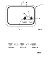
- a communication device (1) is in the form of a contactless smart card. However, it could take other forms including flush contact card, USB key or other.
- This device is intended to communicate with a terminal (2) adapted to the type of communication supported by the chip via communication signals (R).
- the signals are of the ISO 14443 type, but could be other, in particular ISO 7616 for an interface with electrical contacts.
- the device comprises at least two microcircuits or components (3, 4), in this case two integrated circuit chips. These chips are in the example mounted on modules presenting an insulating support and connection pads connected to at least a part of a communication interface. Part may include in particular a few pads of a terminal block of electrical contacts among a set of pads.
- the microcircuits or components 3, 4 are connected in parallel to at least one common part of a communication interface (5).
- This is a radiofrequency antenna 5 having turns disposed at the periphery of the edge of the card.
- Selection means (6) for one of the microcircuits equip the device. According to one characteristic of this embodiment, these selection means are able to be actuated in response to an interaction with the outside; this interaction is distinct from the communication signals used in the implementation of the applications loaded in the microcircuits.
- the interaction does not take place via the same interface as that used for the communication between the microcircuits and the terminal.
- the messages conveyed by the modulated communication signals are not used to operate a selector.
- the invention thus has the advantage of dispensing with a compatible protocol or reader or coding and decoding means for actuating a selector of components in the device.
- the selection means are manually operable by the user.
- a switch according to a schematic diagram electric. Any type of mechanical switch, electrical, contact, push, ohmic or other can be used.
- the invention may comprise more complex switches, with multi connections, bi stable switches or others including those comprising a sensor sensitive to external radiation or other activator.
- the sensor may for example be an infrared sensor, a temperature sensor of the human body by applying a finger to a suitable cell, a pressure sensor, a sensitive sensor such as those of the sensory screens, etc.
- one of the microcircuits has priority in establishing communication with respect to the other microcircuit when they are connected in parallel and in that said selection means intervene to connect or disconnect the priority microcircuit to the microcircuit. interface.
- the microcircuit (3) is of priority type with respect to the other (4) vis-à-vis the receipt of a communication from a terminal.
- it is a chip type "Mifare” type A founders such as NXP or Infineon companies etc.
- This priority management can be done in the programming of the communication in the terminal itself (in the example Type A).
- this priority can be reversed and therefore have priority over type B for chips of founders such as Infinite, ST Microelectronics, Samsung, etc. and in this case a permutation will have to be carried out between the chips type A and B of the figure 1 .
- Priority can also come from the chip-specific response time.
- the chip B can contain an application corresponding to the standard "Calypso" of "Calypso Founders Association", defining security dialogues between terminals and cards.
- the selection means here comprise a switch positioned on at least one link of the priority microcircuit to the interface, while the non-priority chip is always connected to the interface regardless of the state of the switch.
- the electrical assembly is carried out in such a way that the priority chip of type A is connected secondly with respect to the non-priority type B chip 4, the antenna connections first connecting chip 4 and then chip 3 by a chip chip bridging.
- Such an assembly above is advantageous especially in the case of a migration of old technology to a more recent because in operation, when closing the circuit, the priority chip is connected and operates at the expense of the other. .
- the circuit or assembly is made in such a way that the chip associated with the new technology comes into operation without having to switch on the switch.
- the priority chip 3 of type A represents the new migration technology
- the non-priority chip 4 of type B representing the current technology
- FIG. 2 To the figure 2 is illustrated a sequence of waking wave train or activation of transponders comprising the elements (3 or 4 and 5).
- Some of the current radio frequency terminals or readers intermittently emit two types of signals intended for at least two types A or B of a chip so as to wake them up (“wake up A” and then "wake up B”). The terminal does so because it ignores a priori what type of chip A or B, it will have to dialogue depending on whether the user holds a single chip card type A or B.
- the switch of the figure 1 is replaced by a push-type mechanical switch; it comprises a metal dome 6a which is positioned on two links coming respectively from a chip stud 3 and 4.
- the push button may include a "Belleville” type dome washer introduced into a cavity provided for this purpose.
- said selection means 16 are operable by an external signal. This may preferably come from the terminal.
- a light signal (L) is emitted by the terminal for example when a person is detected by presence detectors, a light beam (L) or other radiates in this transaction space near the terminal.
- This light signal is captured by the card presented by a user.
- the signal is picked up by a sensor 16 disposed outside the chips 3 and 4.
- This is a photodiode 16 which is busy when it picks up light, thus closing or by passing the circuit on which she is.
- the same references designate the same elements.
- This photodiode is mounted as previously on a bridging link between the two chips.
- the cell of the photodiode opens on the surface or is covered with a transparent or translucent card material.
- the terminal activates the chip 3 or 4 by radiofrequency (R) wave trains via its own-antenna interface, in particular at 13.56 MHz and carries out the planned transactions via the antenna 5 of the map.
- R radiofrequency
- the switch comprises an element sensitive to the communication signals transmitted by the terminal.
- the switch may be a radio frequency sensor and include for example a suitable antenna.
- the sensor can preferably be set to very quickly capture the radio frequency signals before or at the same time that the woken chip does not begin to communicate and do a complete transaction to the end (authentication, payment, access ).
- this sensor may comprise a flat antenna or coil of the antenna type 5 and activate a relay or a circuit breaker under the effect of a wave train such as that used for waking the chips illustrated in FIG. the figure 2 .
- the maintenance of the switch can possibly be carried out by a timer coupled to the switch and which will collect radio frequency energy and store it for example in a capacity.
- the maintenance energy of the switch can be performed in particular by the discharge of the capacity.
- the invention does not use the signals of the reader but only in this case the energy of the radio frequency waves used to convey the signals or communication messages. There is therefore no need either in this case to code or decode signals from the terminal. The invention therefore ignores the protocol used by the reader to select a microcircuit or an application
- the switch is disposed outside the chips, so as not to have to change them and for simplicity of implementation.
- an internal arrangement of the switch in one and / or other chip (s) in integrated form could also be provided by the invention.
- the advantage here is to overcome a terminal communication protocol which is useful during a migration.
- the chips are selected automatically by equipping the readers either with a radiation emitter (L) in particular light (or other such as infrared ...) and by providing the appropriate switch accordingly in the device.
- a radiation emitter L in particular light (or other such as infrared )
- the radiation activates a photodiode to cut the circuit of a priority chip or type A microcircuit belonging to a long-time technology to be replaced.
- the terminal no longer emits radiation (the latter having been deactivated) and the chip type B belonging to the new technology remains enabled by default automatically.
- the priority chip 3 type A is activated by default without radiation because its circuit is closed by default at rest without radiation, then under the effect of radiation or other activation of the switch or contactor, the circuit opens leaving thus the communication to the other non-priority chip but representing the new migration technology.
- This mode of operation has the advantage of offering more security because it must be close to the terminal to close the circuit, the user does not even have to operate himself the switch.
- the invention allows to use two or more chips of different or identical type for applications or reserved uses.
- a user may reserve a chip for small current transactions and use another chip for larger amounts.
- the chips may have different security features depending on the application.
- a chip can be used for access in a company, to pay the company restaurant, to pay in drink dispensers while the other chip is used to connect to a computer or to authenticate on a network by putting in create prerecorded passwords ...
- Another use is to reserve one chip for storage of non-sensitive data while the other implements Cipher operations and specific session keys.
- the implementation is different, especially over time.
- a user can use a chip containing sensitive data for trust transactions and another for risky transactions with an outside world, the advantage being that the chips are perfectly compartmentalized and can thus include secrets of different operators. .
- the priority chip is dedicated to large transactions and requires a voluntary operation of the user as a pressure on a push button to validate or allow a transaction including contactless.
- This chip 3 is connected as on the figure 3 while the non-priority type B chip 4 is used for transactions of a lower amount such as switching to the subway by operating as an electronic purse for small financial transactions.
- the invention therefore provides a simple way to gain flexibility in use according to the uses and / or applications at the discretion of the user with the possible additional security and control over operations with a single card.
- the microcircuit selection means 3, 4 may comprise a keypad with two or more keys for entering an access code to one or the other microcircuit.
- the invention may comprise "n" microcircuits and "n” applications, the selection means for selecting each microcircuit and / or application.
- the switch can also be an incrementing selector or switching from one microcircuit to another with each intervention of the user.
Landscapes
- Engineering & Computer Science (AREA)
- Computer Hardware Design (AREA)
- Microelectronics & Electronic Packaging (AREA)
- Physics & Mathematics (AREA)
- General Physics & Mathematics (AREA)
- Theoretical Computer Science (AREA)
- Computer Security & Cryptography (AREA)
- General Engineering & Computer Science (AREA)
- Credit Cards Or The Like (AREA)
- Near-Field Transmission Systems (AREA)
Priority Applications (4)
| Application Number | Priority Date | Filing Date | Title |
|---|---|---|---|
| EP09305326A EP2242005A1 (de) | 2009-04-16 | 2009-04-16 | Kommunikationsvorrichtung mit zwei über eine gemeinsame Kommunikationsschnittstelle verbundenen Chips |
| PCT/EP2010/054119 WO2010118947A1 (fr) | 2009-04-16 | 2010-03-29 | Dispositif de communication comportant deux puces a interface de communication commune |
| EP10711673.3A EP2419865B1 (de) | 2009-04-16 | 2010-03-29 | Kommunikationsvorrichtung mit zwei über eine gemeinsame kommunikationsschnittstelle verbundenen chips |
| ES10711673.3T ES2538397T3 (es) | 2009-04-16 | 2010-03-29 | Dispositivo de comunicación que incluye dos chips con una interfaz de comunicación común |
Applications Claiming Priority (1)
| Application Number | Priority Date | Filing Date | Title |
|---|---|---|---|
| EP09305326A EP2242005A1 (de) | 2009-04-16 | 2009-04-16 | Kommunikationsvorrichtung mit zwei über eine gemeinsame Kommunikationsschnittstelle verbundenen Chips |
Publications (1)
| Publication Number | Publication Date |
|---|---|
| EP2242005A1 true EP2242005A1 (de) | 2010-10-20 |
Family
ID=40941812
Family Applications (2)
| Application Number | Title | Priority Date | Filing Date |
|---|---|---|---|
| EP09305326A Withdrawn EP2242005A1 (de) | 2009-04-16 | 2009-04-16 | Kommunikationsvorrichtung mit zwei über eine gemeinsame Kommunikationsschnittstelle verbundenen Chips |
| EP10711673.3A Active EP2419865B1 (de) | 2009-04-16 | 2010-03-29 | Kommunikationsvorrichtung mit zwei über eine gemeinsame kommunikationsschnittstelle verbundenen chips |
Family Applications After (1)
| Application Number | Title | Priority Date | Filing Date |
|---|---|---|---|
| EP10711673.3A Active EP2419865B1 (de) | 2009-04-16 | 2010-03-29 | Kommunikationsvorrichtung mit zwei über eine gemeinsame kommunikationsschnittstelle verbundenen chips |
Country Status (3)
| Country | Link |
|---|---|
| EP (2) | EP2242005A1 (de) |
| ES (1) | ES2538397T3 (de) |
| WO (1) | WO2010118947A1 (de) |
Cited By (1)
| Publication number | Priority date | Publication date | Assignee | Title |
|---|---|---|---|---|
| FR2968803A1 (fr) * | 2010-12-10 | 2012-06-15 | St Microelectronics Rousset | Communication sans contact avec autorisation par photodiode |
Families Citing this family (2)
| Publication number | Priority date | Publication date | Assignee | Title |
|---|---|---|---|---|
| CN102468988A (zh) * | 2010-11-11 | 2012-05-23 | 上海华虹集成电路有限责任公司 | 自动检测iso/iec14443协议中信号协议类型的装置 |
| GB201506954D0 (en) | 2015-04-23 | 2015-06-10 | Royal College Of Art | Communications device system and method |
Citations (4)
| Publication number | Priority date | Publication date | Assignee | Title |
|---|---|---|---|---|
| FR2680262A1 (fr) | 1991-08-08 | 1993-02-12 | Gemplus Card Int | Circuits integres pour carte a puce et carte a plusieurs puces utilisant ces circuits. |
| EP0779598A2 (de) * | 1995-12-14 | 1997-06-18 | Hitachi, Ltd. | Multichip-IC-Karte und Verwendungssystem |
| EP1267303A1 (de) | 2001-06-11 | 2002-12-18 | cubit electronics Gmbh | Transponder |
| US20070194926A1 (en) * | 1999-05-06 | 2007-08-23 | Bayley Oliver T | Interactive radio frequency tags |
Family Cites Families (1)
| Publication number | Priority date | Publication date | Assignee | Title |
|---|---|---|---|---|
| FR2637710A1 (fr) * | 1988-10-07 | 1990-04-13 | B Et Dev | Procede et dispositif de commande electronique multifonction a haute securite comportant une carte a puce |
-
2009
- 2009-04-16 EP EP09305326A patent/EP2242005A1/de not_active Withdrawn
-
2010
- 2010-03-29 ES ES10711673.3T patent/ES2538397T3/es active Active
- 2010-03-29 EP EP10711673.3A patent/EP2419865B1/de active Active
- 2010-03-29 WO PCT/EP2010/054119 patent/WO2010118947A1/fr not_active Ceased
Patent Citations (4)
| Publication number | Priority date | Publication date | Assignee | Title |
|---|---|---|---|---|
| FR2680262A1 (fr) | 1991-08-08 | 1993-02-12 | Gemplus Card Int | Circuits integres pour carte a puce et carte a plusieurs puces utilisant ces circuits. |
| EP0779598A2 (de) * | 1995-12-14 | 1997-06-18 | Hitachi, Ltd. | Multichip-IC-Karte und Verwendungssystem |
| US20070194926A1 (en) * | 1999-05-06 | 2007-08-23 | Bayley Oliver T | Interactive radio frequency tags |
| EP1267303A1 (de) | 2001-06-11 | 2002-12-18 | cubit electronics Gmbh | Transponder |
Cited By (1)
| Publication number | Priority date | Publication date | Assignee | Title |
|---|---|---|---|---|
| FR2968803A1 (fr) * | 2010-12-10 | 2012-06-15 | St Microelectronics Rousset | Communication sans contact avec autorisation par photodiode |
Also Published As
| Publication number | Publication date |
|---|---|
| ES2538397T3 (es) | 2015-06-19 |
| WO2010118947A1 (fr) | 2010-10-21 |
| EP2419865B1 (de) | 2014-11-26 |
| EP2419865A1 (de) | 2012-02-22 |
Similar Documents
| Publication | Publication Date | Title |
|---|---|---|
| EP2172877B1 (de) | Elektronisches Gerät und dazu beitragendes kontaktloses Kommunikationsmanagement, und ein Hostgerät | |
| EP2507747B1 (de) | Aktivierung und anzeige eines hf-feldes auf einer vorrichtung mit einem chip | |
| EP2220597B1 (de) | System mit integriertem doppeltem schaltkreis und verwendung dieses systems zum einsatz einer remote-anwendung | |
| EP2612447B1 (de) | Sicherung einer telekommunikationsvorrichtung mit einem nahfeldkommunikationsmodul | |
| EP2218040B1 (de) | Hochfrequenzkommunikationseinrichtung mit einem timer | |
| EP2194491A1 (de) | Elektronische Karte, die Steuermittel umfasst | |
| EP2131313A1 (de) | Verfahren zur Anwendungsauswahl in einem drahtlosen mobilen Kommunikationsgerät in einem NFC-System und entsprechendes drahtloses mobiles Kommunikationsgerät | |
| FR2892212A1 (fr) | Lecteur nfc ayant un mode de fonctionnement passif a faible consommation electrique | |
| FR2942365A1 (fr) | Dispositif de communication incluant une batterie et un module de communication a champ proche | |
| FR2923634A1 (fr) | Carte a microprocesseur, telephone comprenant une telle carte et procede d'execution d'une commande dans une telle carte. | |
| EP1496470A1 (de) | Kombi-Chipkarte | |
| EP2419865B1 (de) | Kommunikationsvorrichtung mit zwei über eine gemeinsame kommunikationsschnittstelle verbundenen chips | |
| EP3110190B1 (de) | Verfahren und vorrichtung zur verwaltung von kontaktlosen anwendungen | |
| FR2923632A1 (fr) | Carte a microprocesseur, telephone comprenant une telle carte et procede de traitement dans une telle carte. | |
| EP2582113A1 (de) | Adaptationsvorrichtung zwischen einem kontaktlosen Lesegerät und einem Funkgerät | |
| EP2577574A1 (de) | Bankkarte mit anzeigeschirm | |
| EP2254077A1 (de) | Vorrichtung für konventionelle Chipkarte, die eine elektronische Transaktion über ein Netz erlaubt | |
| EP2251818B1 (de) | Elektronische Einheit, die als Kartenleser funktionieren kann, Mikrochipkarte und entsprechende Verfahren | |
| EP1048003A1 (de) | System zur gesicherten kontaktlosen kommunikation zwischen einem endgerat und einem tragbaren gegenstand wie eine chipkarte | |
| FR2770315A1 (fr) | Systeme pour la communication securisee sans contact entre un terminal et un objet portatif tel qu'une carte a puce | |
| EP0639486A1 (de) | Alarmsystem für eine mobile Funkstation | |
| EP2202677B1 (de) | Chipkarte und mobiles Endgerät, das eine solche Karte umfasst | |
| FR2819910A1 (fr) | Interconnexion de micromdules de cartes a puce et dispositif electronique portable comprenant une pluralite de micromodules de cartes a puce, connectes en reseau | |
| EP2401706B1 (de) | Tragbare vorrichtung, insbesondere usb-flash-laufwerk, die mit mehreren wählbaren kontaktlosen kommunikationsschnittstellen versehen ist | |
| CH700045A2 (fr) | Carte electronique ayant des moyens de commande. |
Legal Events
| Date | Code | Title | Description |
|---|---|---|---|
| PUAI | Public reference made under article 153(3) epc to a published international application that has entered the european phase |
Free format text: ORIGINAL CODE: 0009012 |
|
| AK | Designated contracting states |
Kind code of ref document: A1 Designated state(s): AT BE BG CH CY CZ DE DK EE ES FI FR GB GR HR HU IE IS IT LI LT LU LV MC MK MT NL NO PL PT RO SE SI SK TR |
|
| AX | Request for extension of the european patent |
Extension state: AL BA RS |
|
| STAA | Information on the status of an ep patent application or granted ep patent |
Free format text: STATUS: THE APPLICATION IS DEEMED TO BE WITHDRAWN |
|
| 18D | Application deemed to be withdrawn |
Effective date: 20110421 |