EP2241997B1 - Memory card reader - Google Patents
Memory card reader Download PDFInfo
- Publication number
- EP2241997B1 EP2241997B1 EP10159587A EP10159587A EP2241997B1 EP 2241997 B1 EP2241997 B1 EP 2241997B1 EP 10159587 A EP10159587 A EP 10159587A EP 10159587 A EP10159587 A EP 10159587A EP 2241997 B1 EP2241997 B1 EP 2241997B1
- Authority
- EP
- European Patent Office
- Prior art keywords
- memory card
- printed circuit
- intrusion device
- card reader
- intrusion
- Prior art date
- Legal status (The legal status is an assumption and is not a legal conclusion. Google has not performed a legal analysis and makes no representation as to the accuracy of the status listed.)
- Active
Links
Images
Classifications
-
- G—PHYSICS
- G06—COMPUTING OR CALCULATING; COUNTING
- G06K—GRAPHICAL DATA READING; PRESENTATION OF DATA; RECORD CARRIERS; HANDLING RECORD CARRIERS
- G06K7/00—Methods or arrangements for sensing record carriers, e.g. for reading patterns
- G06K7/0013—Methods or arrangements for sensing record carriers, e.g. for reading patterns by galvanic contacts, e.g. card connectors for ISO-7816 compliant smart cards or memory cards, e.g. SD card readers
- G06K7/0021—Methods or arrangements for sensing record carriers, e.g. for reading patterns by galvanic contacts, e.g. card connectors for ISO-7816 compliant smart cards or memory cards, e.g. SD card readers for reading/sensing record carriers having surface contacts
-
- G—PHYSICS
- G06—COMPUTING OR CALCULATING; COUNTING
- G06K—GRAPHICAL DATA READING; PRESENTATION OF DATA; RECORD CARRIERS; HANDLING RECORD CARRIERS
- G06K7/00—Methods or arrangements for sensing record carriers, e.g. for reading patterns
- G06K7/0013—Methods or arrangements for sensing record carriers, e.g. for reading patterns by galvanic contacts, e.g. card connectors for ISO-7816 compliant smart cards or memory cards, e.g. SD card readers
- G06K7/0086—Methods or arrangements for sensing record carriers, e.g. for reading patterns by galvanic contacts, e.g. card connectors for ISO-7816 compliant smart cards or memory cards, e.g. SD card readers the connector comprising a circuit for steering the operations of the card connector
- G06K7/0091—Methods or arrangements for sensing record carriers, e.g. for reading patterns by galvanic contacts, e.g. card connectors for ISO-7816 compliant smart cards or memory cards, e.g. SD card readers the connector comprising a circuit for steering the operations of the card connector the circuit comprising an arrangement for avoiding intrusions and unwanted access to data inside of the connector
-
- H—ELECTRICITY
- H05—ELECTRIC TECHNIQUES NOT OTHERWISE PROVIDED FOR
- H05K—PRINTED CIRCUITS; CASINGS OR CONSTRUCTIONAL DETAILS OF ELECTRIC APPARATUS; MANUFACTURE OF ASSEMBLAGES OF ELECTRICAL COMPONENTS
- H05K1/00—Printed circuits
- H05K1/02—Details
- H05K1/0275—Security details, e.g. tampering prevention or detection
Definitions
- the present invention relates to the field of protection of memory card reading devices.
- Such memory card reading devices are used in many devices such as payment terminals, authentication or identification devices or content reading devices.
- the present invention relates more particularly to the securing of such memory card reading devices so that it is not possible to capture or monitor signals that are exchanged between a memory card inserted in the device and a secure processor that processes data from this memory card.
- Devices that incorporate memory card reading devices include many security devices and implement many methods to ensure that the devices are used according to the uses for which they were intended and comply with safety standards that are imposed by certification bodies.
- PCI PED 2.0 Payment Card Industry Pin Entry Device
- This new security standard notably consists of securing the keypad for entering terminals by protecting the entry of the confidential code, and blocking the terminal in the event of an intrusion (fraudulent or accidental).
- a first protection is to report a lattice protection circuit of the memory card connector around it and connect this lattice circuit electrically to the electronic card through welds that are not accessible without removing the keyboard. But the keyboard itself is protected from fraudulent disassembly by the presence of false keys that detect the withdrawal of it. Therefore, a simple protection (for example with a lattice circuit on a single side of a flexible printed circuit), provided that it is connected to points inaccessible by a fraudster can be enough to protect four faces on five of the connector of memory card (CAM).
- CAM connector of memory card
- this cache is fixed or removable.
- this cover is pivotally mounted to allow maintenance of the device although it puts it out of service (the pivot can be "sensitive” to trigger a security procedure when you want to access it ).
- the device remains repairable by an authorized person (loss of sensitive information, such as banking information).
- it is an expensive solution that requires an activation operation.
- When mounted fixed on the memory card connector or when this cover is an integral part of the memory card connector it is generally not possible to operate on the memory card connector to perform maintenance on the memory card connector. 'apparatus. You must then replace the entire memory card connector.
- these connectors require an additional step to activate the protection (mechanical operation).
- the covers are generally made of a plastic part or resistant material and a conductive element such as a copper wire.
- a conductive element such as a copper wire.
- the invention does not have the drawbacks of the prior art. Indeed, the invention relates to a memory card reader, comprising a printed circuit on which is mounted a memory card connector, said connector
- the document " ITT MFG ENTREPRISES” ( FR 2,875,036 ) dated March 10, 2006, relates to a memory card connector that includes an anti-intrusion device (page 1, line 5 to 10) in the form of a metal cage (isolated) that surrounds a specific connector to be protected ( 22, 38).
- the memory card connector comprises at least one signal contact blade (22a) and a ground contact blade and having at least one metal plate (42, 50) of protection which extends opposite a portion vis-à-vis the first signal contact blade and which is electrically connected to a ground contact blade.
- memory card reader having a slot for inserting a memory card and a set of contact points for exchanging data between said memory card and a processor mounted on said printed circuit.
- said printed circuit further carries an anti-intrusion device formed and placed so that said anti-intrusion device prevents access, from the outside of said reader, to at least one connection portion between the at least one of said points of contact of said set of contact points and said printed circuit.
- the invention proposes a solution based on fixing directly on the printed circuit, an anti-intrusion device specifically adapted to the cache function of the contact points of the memory card connector.
- the invention thus provides a simple solution to implement and inexpensive since it is sufficient to mount and fix the anti-intrusion device at the appropriate place. This operation can even be carried out after mounting the memory card connector, for example by using a method of transferring components to lead-free printed circuits.
- said anti-intrusion device has substantially the shape of a rectangular parallelepiped comprising, on its upper face, a protrusion of obstructing access to said contact points from above said device Anti-intrusion.
- the anti-intrusion device is, according to the invention, produced according to the techniques for manufacturing printed circuits.
- said anti-intrusion device comprises at least one three-dimensional conductive circuit and at least two contact elements of said conductive circuit with a connection pad of said anti-intrusion device on said printed circuit;
- the anti-intrusion device is tamper-proof because a break-in of the latter causes a short circuit in the lattice that it comprises, thus triggering an action at the level of the safe processor.
- said printed circuit comprises a zone intended to receive said anti-intrusion device which comprises an even number of connection pads of said anti-intrusion device.
- said ranges consist of at least two separate parts a space for, during the fixing of said anti-intrusion device on said printed circuit, an air outlet resulting from said fixing.
- the invention also relates to a confidential code input device.
- such a device comprises a memory card reader as described above.
- the invention also relates to an anti-intrusion device, in particular for a memory card reader.
- a device comprises a plurality of superposed printed circuit layers connected to one another by buried vias and in the form of an electronic component able to be electrically connected to a circuit. printed on which it is mounted.
- the invention in another aspect, relates to a method of securing an electronic component mounted on a printed circuit.
- a method of securing an electronic component mounted on a printed circuit comprises a step of setting, together with said electronic component to be secured, an anti-intrusion device comprising a plurality of superimposed printed circuit layers connected to each other by means of vias. buried able to be electrically connected to a printed circuit board on which it is mounted.
- the invention proposes to protect frontally the contact points of the memory card connector by adding, on the printed circuit, an anti-intrusion device. Since the anti-intrusion device is mounted on the circuit board, and not on the memory card connector, it is easier to mount. In addition, it is easier to build an anti-intrusion device that is directly mounted on the printed circuit than to build an anti-intrusion device that must be integrated in the memory card connector itself.
- the anti-intrusion device is a surface-mounted electronic component (CMS).
- CMS surface-mounted electronic component
- the anti-intrusion device of the invention can be shaped in order to receive, within it, a electronic circuit to protect, thus forming a protective enclosure within which may be a sensitive electronic circuit that is to be protected.
- the anti-intrusion device of the invention can be used not only to protect contact points, such as input / output contact points, but also printed circuits in their entirety, thereby preventing any attempt monitoring, for example a processor located within the device.
- the anti-intrusion device comprises a plurality of superimposed printed circuit layers and interconnected by means of buried vias and in that it is in the form of an electronic component.
- a device can be in any form.
- the shape of the device can be adapted according to the component or printed circuit to be protected.
- a protection is provided for an electronic component mounted on a printed circuit by performing a setting step, together with the electronic component to be secured, of an anti-intrusion device.
- this joint setting step ensures that it is not possible to alter the electronic component to be secured.
- a memory card reader in which an anti-intrusion device has been mounted on the printed circuit in order to prevent access to the contact points, whose point of contact said IO "(of English for" Input / output ").
- the memory card connector (12) is mounted on the printed circuit (13).
- the memory card connector has a slot (12.1) into which the card can be inserted.
- the memory card connector also includes a set of contacts (12.2) for connection of the card, once inserted, with a processor of the apparatus.
- These contacts (12.2) have a slight bulge (12.3) at the connection area with the card within the memory card connector.
- the contacts are then shaped so that they extend towards the printed circuit (13). They join it at an intermediate zone in which the contact points (12.4) are connected to the printed circuit (13).
- the anti-intrusion device (14) is mounted so that it prevents access to at least some points of contact and in particular to the contact "IO".
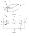
- the latter can advantageously comprise an obstruction protrusion (14.1), which is an element whose width or length is greater than the width or length of the body of the anti-intrusion device and which serves to mask the contact points (12.4) of the memory card connector, as shown in FIG. figure 3 .
- contact elements such as thin electrical wires or thin conductive films
- the anti-intrusion device comprises at least one three-dimensional conductive circuit and at least two elements allowing contact of the three-dimensional conductive circuit with a connection pad. of the anti-intrusion device on the printed circuit. More particularly, the anti-intrusion device is called lattice since the conductive circuit it contains realizes a three-dimensional grid of the volume of the anti-intrusion device.
- Such a grid is produced, according to the invention, by placing on top of one another several printed circuit layers in accordance with conventional technologies so as to form an anti-intrusion device whose volume makes it possible to protect access to the points of contact. contact.
- buried vias are made between two successive layers.
- a via is a metallized hole which is intended to electrically connect different layers of the printed circuit.
- the anti-intrusion device can also be covered again with a membrane and thus constitute a surface-mounted component which itself incorporates a surface-mounted component.
- the anti-intrusion device 14 is mounted on the printed circuit 13.
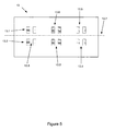
- the printed circuit has, as usual, tracks (13.1 to 13.6) which allow the contact or conductive circuit of the device anti-intrusion with the circuit board or circuits.
- the printed circuit has, in the mounting area of the anti-intrusion device, an even number of contacting pads, the pads being arranged symmetrically along an imaginary axis of positioning ( 13.7).
- the inventors have noticed that during the fixing of the surface-mounted components on the printed circuit, a lateral force is exerted on the surface-mounted component causing its rotation.
- the inventors have discovered that one of the variables which determines the degree of rotation of the surface-mounted component once fixed with respect to the mounting position the same component is the number of attachment areas and their positions relative to each other.
- the inventors have discovered that once mounted, during the action of fasteners, the component tends to adopt a symmetrical position with respect to the attachment areas.
- the position in which the anti-intrusion device is fixed is the position in which the anti-intrusion device is mounted. Indeed, if once fixed, the anti-intrusion device is inclined at least a few degrees from its mounting position, its protective action can be reduced or completely canceled.
- the inventors therefore had the idea of placing an even number of attachment areas for the anti-intrusion device, these ranges being distributed symmetrically along a positioning axis.
- the forces exerted during the fixing are identical on all the ranges and the component is fixed in the same position as that in which it was mounted.
- the reception ranges (13.1 to 13.6) have been separated by a space (13.8) not including copper.
- the space left free on the beach makes it possible to receive the air which comes from the fixing and to provide a weld perfectly free of air pockets.
- Guard tracks are also positioned around each weld 13.1 to 13.6. These guard tracks make it possible to avoid a short circuit of the contact points by performing a lateral attack. These guard tracks have the shape of a rectangle that surrounds the reception ranges and are electrically connected to the secure processor so that the latter can detect a short circuit.
Landscapes
- Engineering & Computer Science (AREA)
- Artificial Intelligence (AREA)
- Computer Vision & Pattern Recognition (AREA)
- Physics & Mathematics (AREA)
- General Physics & Mathematics (AREA)
- Theoretical Computer Science (AREA)
- Computer Security & Cryptography (AREA)
- Microelectronics & Electronic Packaging (AREA)
- Storage Device Security (AREA)
- Credit Cards Or The Like (AREA)
- Coupling Device And Connection With Printed Circuit (AREA)
- Details Of Connecting Devices For Male And Female Coupling (AREA)
Abstract
Description
La présente invention se rapporte au domaine de la protection des dispositifs de lecture de cartes mémoire. De tels dispositifs de lecture de carte mémoire sont employés dans de nombreux appareils tels que des terminaux de paiement, des dispositifs d'authentification ou d'identification ou encore des dispositifs de lecture de contenus.The present invention relates to the field of protection of memory card reading devices. Such memory card reading devices are used in many devices such as payment terminals, authentication or identification devices or content reading devices.
La présente invention se rapporte plus particulièrement à la sécurisation de tels dispositifs de lecture de cartes mémoire afin qu'il ne soit pas possible de capter ou de surveiller des signaux qui sont échangés entre une carte mémoire insérée dans le dispositif et un processeur sécurisé qui traite des données issues de cette carte mémoire.The present invention relates more particularly to the securing of such memory card reading devices so that it is not possible to capture or monitor signals that are exchanged between a memory card inserted in the device and a secure processor that processes data from this memory card.
Les appareils qui intègrent des dispositifs de lecture de carte mémoire, tels que des terminaux de paiement, comprennent de nombreux dispositifs de sécurisation et mettent en oeuvre de nombreuses méthodes permettant d'assurer que les appareils sont utilisés conformément aux usages pour lesquels ils ont été prévus et respectent des normes de sécurité qui sont imposés par des organismes de certification.Devices that incorporate memory card reading devices, such as payment terminals, include many security devices and implement many methods to ensure that the devices are used according to the uses for which they were intended and comply with safety standards that are imposed by certification bodies.
Par exemple, dans le domaine des terminaux de paiement pour cartes à puces, les fabricants sont contraints de respecter depuis de 1er Janvier 2008, la norme PCI PED 2.0 (Payment Card Industry Pin Entry Device).For example, in the field of payment terminals for smart cards, manufacturers have been forced to comply since 1 January 2008, PCI PED 2.0 (Payment Card Industry Pin Entry Device).
Cette nouvelle norme sécuritaire consiste notamment à sécuriser le clavier de saisie des terminaux en protégeant la saisie du code confidentiel, et à bloquer le terminal en cas d'intrusion (frauduleuse ou accidentelle).This new security standard notably consists of securing the keypad for entering terminals by protecting the entry of the confidential code, and blocking the terminal in the event of an intrusion (fraudulent or accidental).
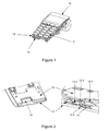
On présente, en relation avec la
- un clavier (11) sur sa face supérieure ;
- un connecteur de carte à mémoire (12) parfois placé sous le clavier et qui permet d'introduire la carte et de dialoguer avec elle. Ce connecteur de carte à mémoire (12) est fixé, généralement par soudure, à un circuit imprimé (13).
- a keyboard (11) on its upper face;
- a memory card connector (12) sometimes placed under the keyboard and which allows to introduce the card and dialogue with it. This connector memory card (12) is fixed, usually by soldering, to a printed circuit (13).
Afin de protéger le terminal il a parfois été jugé intéressant de combiner les sécurités sur ces deux organes. Une première protection consiste à rapporter un circuit treillis de protection du connecteur carte à mémoire autour de celui-ci et de relier ce circuit treillis électriquement à la carte électronique par l'intermédiaire de soudures qui ne sont pas accessibles sans enlever le clavier. Or le clavier est lui-même protégé d'un démontage frauduleux par la présence de fausses touches qui détectent le retrait de celui-ci. De ce fait, une protection simple (par exemple avec un circuit treillis sur une seule face d'un circuit imprimé souple), pourvu qu'elle soit connectée en des points inaccessibles par un fraudeur peut suffire à protéger quatre faces sur cinq du connecteur de carte à mémoire (CAM).In order to protect the terminal it has sometimes been considered interesting to combine security on these two bodies. A first protection is to report a lattice protection circuit of the memory card connector around it and connect this lattice circuit electrically to the electronic card through welds that are not accessible without removing the keyboard. But the keyboard itself is protected from fraudulent disassembly by the presence of false keys that detect the withdrawal of it. Therefore, a simple protection (for example with a lattice circuit on a single side of a flexible printed circuit), provided that it is connected to points inaccessible by a fraudster can be enough to protect four faces on five of the connector of memory card (CAM).
La dernière face servant à l'introduction de la carte du client ne peut bien sûr pas être fermée. Il reste donc, dans ce cas précis, un angle d'attaque au fraudeur pour atteindre des points de contact (pins) du connecteur, et notamment les points de contacts par lesquels transitent les signaux d'entrées/sorties (dits I/O).The last side used to introduce the customer's card can not of course be closed. It remains therefore, in this specific case, an angle of attack to the fraudster to reach contact points (pins) of the connector, and in particular the points of contact through which the input / output signals (so-called I / O) .
En effet, le connecteur de carte à mémoire de part son implantation sur le circuit imprimé définit trois zones :
- une zone principale de connexion avec la carte mémoire qui permet de lire les informations présentes sur la carte ;
- une zone de liaison qui est noyée dans le connecteur de carte à mémoire ;
- une zone intermédiaire dans laquelle les points de contact sont reliés au circuit imprimé.
- a main zone of connection with the memory card which makes it possible to read the information present on the card;
- a link area which is embedded in the memory card connector;
- an intermediate zone in which the contact points are connected to the printed circuit.
Il était nécessaire de se prémunir d'un accès frauduleux à ces points de contact. En effet, il est fort possible d'imaginer connecter, au niveau de ces points de contact, un dispositif de surveillance qui pourrait être utilisé pour enregistrer les signaux qui transiteraient entre le processeur et la carte à puce. Un tel enregistrement pourrait conduire à une obtention de données sensibles. On doit donc protéger ces points de contact, au niveau de la zone intermédiaire, par un système n'interférant pas avec la fonctionnalité du connecteur de carte à mémoire.It was necessary to guard against fraudulent access to these points of contact. Indeed, it is quite possible to imagine connecting at these points of contact, a monitoring device that could be used to record the signals that pass between the processor and the smart card. Such registration could lead to obtaining sensitive data. We have to therefore protect these points of contact, at the intermediate zone, by a system that does not interfere with the functionality of the memory card connector.
Une telle sécurisation est réalisée à l'aide de plusieurs technologies matérielles et logicielles.Such security is achieved using several hardware and software technologies.
Au niveau matériel, certains constructeurs ont directement intégrés un cache au niveau du connecteur de carte à mémoire. Selon les constructeurs, ce cache est fixe ou amovible. Lorsqu'il est amovible, ce cache est monté pivotant pour permettre une maintenance de l'appareil bien qu'il le mette hors service (le pivot permet d'être "sensible" pour déclencher une procédure de sécurisation lorsque l'on veut y accéder). L'appareil reste réparable par une personne habilitée (perte des informations sensibles, telles que les informations bancaires). C'est cependant une solution onéreuse qui nécessite une opération d'activation. Lorsqu'il est monté fixe sur le connecteur de carte à mémoire ou lorsque ce cache fait intégralement partie du connecteur de carte à mémoire, il n'est généralement pas possible d'intervenir sur le connecteur de carte à mémoire pour réaliser une maintenance de l'appareil. Il faut alors remplacer l'intégralité du connecteur de carte à mémoire. De plus, ces connecteurs nécessitent une étape supplémentaire pour activer la protection (opération mécanique).At the hardware level, some vendors have directly integrated a cache at the memory card slot. According to the manufacturers, this cache is fixed or removable. When removable, this cover is pivotally mounted to allow maintenance of the device although it puts it out of service (the pivot can be "sensitive" to trigger a security procedure when you want to access it ). The device remains repairable by an authorized person (loss of sensitive information, such as banking information). However, it is an expensive solution that requires an activation operation. When mounted fixed on the memory card connector or when this cover is an integral part of the memory card connector, it is generally not possible to operate on the memory card connector to perform maintenance on the memory card connector. 'apparatus. You must then replace the entire memory card connector. In addition, these connectors require an additional step to activate the protection (mechanical operation).
De plus, dans les solutions de l'art antérieur, les caches sont généralement constitués d'une pièce en plastique ou en matériau résistant et d'un élément conducteur tel qu'un fil de cuivre. Or la fabrication d'un tel cache, qui ne mesure pas plus de quelques millimètres, en intégrant à la fois des éléments non conducteurs et des éléments conducteurs est complexe.In addition, in the solutions of the prior art, the covers are generally made of a plastic part or resistant material and a conductive element such as a copper wire. However, the manufacture of such a cover, which does not measure more than a few millimeters, by integrating both non-conductive elements and conductive elements is complex.
Il était donc nécessaire de trouver une solution de protection simple et peu coûteuse et qui permettent de réaliser une maintenance de l'appareil sans rendre celui-ci inutilisable. « suite page 3a»It was therefore necessary to find a simple and inexpensive protection solution that allows the maintenance of the device without rendering it unusable. «Continued on page 3a»
L'invention ne présente pas les inconvénients de l'art antérieur. En effet, l'invention concerne un Lecteur de carte à mémoire, comprenant un circuit imprimé sur lequel est monté un connecteur de carte à mémoire, ledit connecteurThe invention does not have the drawbacks of the prior art. Indeed, the invention relates to a memory card reader, comprising a printed circuit on which is mounted a memory card connector, said connector
Le document « ITT MFG ENTREPRISES », (
Selon l'invention, ledit circuit imprimé porte en outre un dispositif anti-intrusion formé et placé de sorte que ledit dispositif anti-intrusion empêche l'accès, à partir de l'extérieur dudit lecteur, à au moins une portion de connexion entre au moins un desdits points de contact dudit ensemble de points de contact et ledit circuit imprimé.According to the invention, said printed circuit further carries an anti-intrusion device formed and placed so that said anti-intrusion device prevents access, from the outside of said reader, to at least one connection portion between the at least one of said points of contact of said set of contact points and said printed circuit.
Ainsi, il n'est pas possible d'accéder aux pins du connecteur pour obtenir, de manière frauduleuse, les signaux qui transitent entre la carte à mémoire et le processeur. En effet, là où les dispositifs de l'art antérieur proposaient des solutions consistant à masquer les pins directement au niveau des connecteurs de carte à mémoire, par exemple en proposant un cache en plastique, l'invention propose une solution basée sur la fixation directement sur le circuit imprimé, d'un dispositif anti-intrusion spécifiquement adapté à la fonction de cache des points de contact du connecteur de cartes à mémoire. L'invention apporte ainsi une solution simple à mettre en oeuvre et peu coûteuse puisqu'il suffit de monter et de fixer le dispositif anti-intrusion à l'endroit idoine. Cette opération peut même être réalisée après le montage du connecteur de carte à mémoire, par exemple en utilisant un procédé de report de composants sur des circuits imprimés en procédé sans plomb.Thus, it is not possible to access pins of the connector to fraudulently obtain the signals that pass between the memory card and the processor. Indeed, where the devices of the prior art proposed solutions consisting of masking the pins directly at the memory card connectors, for example by providing a plastic cover, the invention proposes a solution based on fixing directly on the printed circuit, an anti-intrusion device specifically adapted to the cache function of the contact points of the memory card connector. The invention thus provides a simple solution to implement and inexpensive since it is sufficient to mount and fix the anti-intrusion device at the appropriate place. This operation can even be carried out after mounting the memory card connector, for example by using a method of transferring components to lead-free printed circuits.
Selon un mode de réalisation particulier de l'invention, ledit dispositif anti-intrusion a sensiblement la forme d'un parallélépipède rectangle comprenant, en sa face supérieure, une protubérance d'obstruction de l'accès auxdits points de contact par le dessus dudit dispositif anti-intrusion. Le dispositif anti-intrusion est, selon l'invention, réalisé selon les techniques de fabrication des circuits imprimés.According to a particular embodiment of the invention, said anti-intrusion device has substantially the shape of a rectangular parallelepiped comprising, on its upper face, a protrusion of obstructing access to said contact points from above said device Anti-intrusion. The anti-intrusion device is, according to the invention, produced according to the techniques for manufacturing printed circuits.
Selon un mode de réalisation particulier de l'invention, ledit dispositif anti-intrusion comprend au moins un circuit conducteur tridimensionnel et au moins deux éléments de contact dudit circuit conducteur avec une plage de connexion dudit dispositif anti-intrusion sur ledit circuit imprimé ;According to a particular embodiment of the invention, said anti-intrusion device comprises at least one three-dimensional conductive circuit and at least two contact elements of said conductive circuit with a connection pad of said anti-intrusion device on said printed circuit;
Ainsi, le dispositif anti-intrusion est inviolable, car une effraction de celui-ci entraîne un court circuit dans le treillis qu'il comprend, déclenchant ainsi une action au niveau du processeur sécuritaireThus, the anti-intrusion device is tamper-proof because a break-in of the latter causes a short circuit in the lattice that it comprises, thus triggering an action at the level of the safe processor.
Selon un mode de réalisation particulier de l'invention, ledit circuit imprimé comprend une zone destinée à recevoir ledit dispositif anti-intrusion laquelle comprend un nombre pair de plages de connexion dudit dispositif anti-intrusion.According to a particular embodiment of the invention, said printed circuit comprises a zone intended to receive said anti-intrusion device which comprises an even number of connection pads of said anti-intrusion device.
Ainsi, lors d'une opération de microfixation, telle qu'une soudure, dudit dispositif anti-intrusion sur ledit circuit imprimé, les forces de mouillage s'exercent de manière uniforme entre ledit dispositif anti-intrusion et ledit circuit imprimé de sorte que ledit CMS ne subit pas de flottement (mouvement, déplacement) lors de la fixation.Thus, during a microfixation operation, such as a weld, of said anti-intrusion device on said printed circuit, the wetting forces are exerted uniformly between said anti-intrusion device and said printed circuit so that said CMS does not float (move, move) when fixing.
Selon une caractéristique particulière de l'invention, lesdites plages sont constituées d'au moins deux parties séparées un espace permettant, lors de la fixation dudit dispositif anti-intrusion sur ledit circuit imprimé, une évacuation d'air qui résulte de ladite fixation.According to a particular feature of the invention, said ranges consist of at least two separate parts a space for, during the fixing of said anti-intrusion device on said printed circuit, an air outlet resulting from said fixing.
L'invention concerne également un dispositif de saisie de code confidentiel.The invention also relates to a confidential code input device.
Selon l'invention, un tel dispositif comprend un lecteur de carte mémoire tel que décrit précédemment.According to the invention, such a device comprises a memory card reader as described above.
L'invention concerne encore un dispositif anti-intrusion, notamment pour lecteur de carte à mémoire. Selon l'invention, un tel dispositif comprend plusieurs couches de circuit imprimé superposées et reliées entre elles à l'aide de vias enterrées et en ce qu'il se présente sous la forme d'un composant électronique apte à être connecté électriquement à un circuit imprimé sur lequel il est monté.The invention also relates to an anti-intrusion device, in particular for a memory card reader. According to the invention, such a device comprises a plurality of superposed printed circuit layers connected to one another by buried vias and in the form of an electronic component able to be electrically connected to a circuit. printed on which it is mounted.
Selon un autre aspect, l'invention concerne un procédé de sécurisation d'un composant électronique monté sur un circuit imprimé. Selon l'invention, un tel procédé comprend une étape de posage, conjointement audit composant électronique à sécuriser, d'un dispositif anti-intrusion comprenant plusieurs couches de circuit imprimé superposées et reliées entre elles à l'aide de vias enterrées apte à être connecté électriquement à un circuit imprimé sur lequel il est monté.In another aspect, the invention relates to a method of securing an electronic component mounted on a printed circuit. According to the invention, such a method comprises a step of setting, together with said electronic component to be secured, an anti-intrusion device comprising a plurality of superimposed printed circuit layers connected to each other by means of vias. buried able to be electrically connected to a printed circuit board on which it is mounted.
D'autres caractéristiques et avantages de l'invention apparaîtront plus clairement à la lecture de la description suivante d'un mode de réalisation préférentiel, donné à titre de simple exemple illustratif et non limitatif, et des dessins annexés, parmi lesquels :
- la
figure 1 , déjà commentée, présente une vue globale d'un terminal de paiement intégrant un lecteur de carte à mémoire ; - la
figure 2 illustre un lecteur de carte à mémoire selon l'invention ; - la
figure 3 décrit un dispositif anti-intrusion selon l'invention ; - la
figure 4 décrit un circuit imprimé comprenant des plages de fixation selon l'invention ; - la
figure 5 décrit une plage de fixation selon l'invention.
- the
figure 1 , already commented, presents a global view of a payment terminal incorporating a memory card reader; - the
figure 2 illustrates a memory card reader according to the invention; - the
figure 3 discloses an anti-intrusion device according to the invention; - the
figure 4 discloses a printed circuit comprising fixing pads according to the invention; - the
figure 5 describes a fixing range according to the invention.
L'invention propose de protéger frontalement les points de contacts du connecteur de carte à mémoire en adjoignant, sur le circuit imprimé, un dispositif anti-intrusion. Comme le dispositif anti-intrusion est monté sur le circuit imprimé, et non pas sur le connecteur de carte à mémoire, il est plus simple à monter. De plus, il est plus aisé de construire un dispositif anti-intrusion qui soit directement monté sur le circuit imprimé que de construire un dispositif anti-intrusion qui doive être intégré au connecteur de carte à mémoire lui-même.The invention proposes to protect frontally the contact points of the memory card connector by adding, on the printed circuit, an anti-intrusion device. Since the anti-intrusion device is mounted on the circuit board, and not on the memory card connector, it is easier to mount. In addition, it is easier to build an anti-intrusion device that is directly mounted on the printed circuit than to build an anti-intrusion device that must be integrated in the memory card connector itself.
Selon l'invention, le dispositif anti-intrusion est un composant électronique monté en surface (CMS). Ainsi, le dispositif anti-intrusion peut être monté, sur le circuit imprimé, en même temps que les autres composants dans la même phase de fabrication que les autres composants (l'ordre de posage étant défini lors de la conception de l'appareil).According to the invention, the anti-intrusion device is a surface-mounted electronic component (CMS). Thus, the anti-intrusion device can be mounted on the printed circuit at the same time as the other components in the same manufacturing phase as the other components (the setting order being defined during the design of the apparatus) .
Dans un mode de réalisation de l'invention, il est envisagé que le dispositif anti-intrusion de l'invention puisse être conformé afin de recevoir, en son sein, un circuit électronique à protéger, formant ainsi une enceinte protectrice à l'intérieure de laquelle peut se trouver un circuit électronique sensible que l'on souhaite protéger. Ainsi, le dispositif anti-intrusion de l'invention peut être utilisé non seulement pour protéger des points de contacts, tels que des points de contact d'entrée/sortie, mais également des circuits imprimés dans leur intégralité, en empêchant ainsi une quelconque tentative de surveillance, par exemple d'un processeur se trouvant au sein du dispositif.In one embodiment of the invention, it is envisaged that the anti-intrusion device of the invention can be shaped in order to receive, within it, a electronic circuit to protect, thus forming a protective enclosure within which may be a sensitive electronic circuit that is to be protected. Thus, the anti-intrusion device of the invention can be used not only to protect contact points, such as input / output contact points, but also printed circuits in their entirety, thereby preventing any attempt monitoring, for example a processor located within the device.
En effet, selon l'invention, le dispositif anti-intrusion comprend plusieurs couches de circuit imprimé superposées et reliées entre elles à l'aide de vias enterrées et en ce qu'il se présente sous la forme d'un composant électronique. Un tel dispositif peut se présenter sous n'importe quelle forme. La forme du dispositif peut être adaptée en fonction du composant ou du circuit imprimé à protéger.Indeed, according to the invention, the anti-intrusion device comprises a plurality of superimposed printed circuit layers and interconnected by means of buried vias and in that it is in the form of an electronic component. Such a device can be in any form. The shape of the device can be adapted according to the component or printed circuit to be protected.
Selon l'invention, on réalise une protection d'un composant électronique monté sur un circuit imprimé en réalisant une étape de posage, conjointement au composant électronique à sécuriser, d'un dispositif anti-intrusion. Lorsque le dispositif anti-intrusion forme une enceinte protectrice, cette étape de posage conjointe assure qu'il n'est pas possible d'altérer le composant électronique à sécuriser.According to the invention, a protection is provided for an electronic component mounted on a printed circuit by performing a setting step, together with the electronic component to be secured, of an anti-intrusion device. When the anti-intrusion device forms a protective enclosure, this joint setting step ensures that it is not possible to alter the electronic component to be secured.
Par la suite, on présente un mode de réalisation d'un dispositif lecteur de carte à mémoire selon l'invention. Il est clair cependant que l'invention ne se limite pas à cette application particulière, mais peut également être mise en oeuvre dans de nombreux autres contextes de protection de circuits électroniques et plus généralement dans tous les cas où les caractéristiques listées par la suite sont intéressantes.Subsequently, an embodiment of a memory card reader device according to the invention is presented. It is clear, however, that the invention is not limited to this particular application, but can also be implemented in many other contexts of protection of electronic circuits and more generally in all cases where the features listed hereafter are interesting. .
On présente dans ce mode de réalisation, un lecteur de carte mémoire selon l'invention dans lequel un dispositif anti-intrusion a été monté sur le circuit imprimé afin d'interdire l'accès aux points de contact, dont le point de contact dit « IO » (de l'anglais pour « Input/output »).In this embodiment, a memory card reader according to the invention in which an anti-intrusion device has been mounted on the printed circuit in order to prevent access to the contact points, whose point of contact said IO "(of English for" Input / output ").
Comme illustré en
Ces contacts (12.2) présentent un léger renflement (12.3) au niveau de la zone de connexion avec la carte, au sein du connecteur de carte à mémoire. Les contacts sont ensuite conformés pour qu'ils s'étendent vers le circuit imprimé (13). Ils rejoignent celui-ci au niveau d'une zone intermédiaire dans laquelle les points de contact (12.4) sont reliés au circuit imprimé (13).These contacts (12.2) have a slight bulge (12.3) at the connection area with the card within the memory card connector. The contacts are then shaped so that they extend towards the printed circuit (13). They join it at an intermediate zone in which the contact points (12.4) are connected to the printed circuit (13).
Le dispositif anti-intrusion (14) est monté de sorte qu'il empêche l'accès à au moins certains points de contact et notamment au contact « IO ».The anti-intrusion device (14) is mounted so that it prevents access to at least some points of contact and in particular to the contact "IO".
Afin de se prémunir d'un accès aux points de contact par la face supérieure du dispositif anti-intrusion (14), ce dernier peut avantageusement comprendre une protubérance d'obstruction (14.1), qui est un élément dont la largeur ou la longueur est supérieure respectivement à la largeur ou à la longueur du corps du dispositif anti-intrusion et qui sert à masquer les points de contact (12.4) du connecteur de carte à mémoire, comme présenté en
Ainsi, il n'est pas possible de faire passer des éléments de contact (tels que des minces fils électriques ou des minces films conducteurs) vers les éléments de contact du connecteur de carte à mémoire afin d'espionner les signaux échangés entre la carte à mémoire et le processeur.Thus, it is not possible to pass contact elements (such as thin electrical wires or thin conductive films) to the contact elements of the smart card connector in order to spy on the signals exchanged between the card to be used. memory and the processor.
Afin de se prémunir du perçage du dispositif anti-intrusion en vue d'atteindre les points de contacts, le dispositif anti-intrusion comprend au moins un circuit conducteur tridimensionnel et au moins deux éléments permettant le contact du circuit conducteur tridimensionnel avec une plage de connexion du dispositif anti-intrusion sur le circuit imprimé. Plus particulièrement, le dispositif anti-intrusion est appelé treillis puisque le circuit conducteur qu'il contient réalise un quadrillage tridimensionnel du volume du dispositif anti-intrusion.In order to guard against the piercing of the anti-intrusion device in order to reach the contact points, the anti-intrusion device comprises at least one three-dimensional conductive circuit and at least two elements allowing contact of the three-dimensional conductive circuit with a connection pad. of the anti-intrusion device on the printed circuit. More particularly, the anti-intrusion device is called lattice since the conductive circuit it contains realizes a three-dimensional grid of the volume of the anti-intrusion device.
Un tel quadrillage est réalisé, selon l'invention, en positionnant les unes par-dessus les autres plusieurs couches de circuit imprimé conformément aux technologies classiques de façon à former un dispositif anti-intrusion dont le volume permet de protéger l'accès aux points de contact.Such a grid is produced, according to the invention, by placing on top of one another several printed circuit layers in accordance with conventional technologies so as to form an anti-intrusion device whose volume makes it possible to protect access to the points of contact. contact.
Afin de permettre aux pistes des membranes d'entrer en contact et de former ainsi un véritable circuit tridimensionnel, des vias enterrées sont réalisés entre deux couches successives. Pour mémoire, un via est un trou métallisé qui est destiné à connecter électriquement des différentes couches du circuit imprimé.In order to allow the tracks of the membranes to come into contact and thus form a true three-dimensional circuit, buried vias are made between two successive layers. For the record, a via is a metallized hole which is intended to electrically connect different layers of the printed circuit.
Ainsi, on dispose d'un circuit électrique tridimensionnel dont l'architecture est telle qu'il n'est pas envisageable de le percer sans provoquer un court-circuit et déclencher, selon l'invention une protection active de l'appareil, à savoir par exemple un effacement définitif des mémoires contenant des informations sensibles, que ces mémoires soient situées sur l'appareil lui-même ou sur la carte qui y est insérée.Thus, it has a three-dimensional electrical circuit whose architecture is such that it is not possible to drill without causing a short circuit and trigger, according to the invention an active protection of the device, namely for example a definitive erasure of memories containing sensitive information, these memories are located on the device itself or on the card inserted therein.
Une fois formé, le dispositif anti-intrusion peut également être à nouveau recouvert d'une membrane et constituer ainsi un composant monté en surface qui intègre lui-même un composant monté en surface.Once formed, the anti-intrusion device can also be covered again with a membrane and thus constitute a surface-mounted component which itself incorporates a surface-mounted component.
Selon l'invention, et comme illustré en
En effet, les inventeurs ont remarqué que lors de la fixation des composants montés en surface sur le circuit imprimé, une force latérale est exercée au niveau du composant monté en surface provoquant sa rotation. Les inventeurs ont découvert qu'une des variables qui détermine le degré de rotation du composant monté en surface une fois fixé par rapport à la position de montage de ce même composant est le nombre de plages de fixation et leurs positions les unes par rapport aux autres. Ainsi, les inventeurs ont découvert que une fois monté, lors de l'action des agents de fixations, le composant à tendance à adopter une position symétrique par rapport aux plages de fixation.Indeed, the inventors have noticed that during the fixing of the surface-mounted components on the printed circuit, a lateral force is exerted on the surface-mounted component causing its rotation. The inventors have discovered that one of the variables which determines the degree of rotation of the surface-mounted component once fixed with respect to the mounting position the same component is the number of attachment areas and their positions relative to each other. Thus, the inventors have discovered that once mounted, during the action of fasteners, the component tends to adopt a symmetrical position with respect to the attachment areas.
Or dans le cadre de l'invention, il est important que la position dans laquelle le dispositif anti-intrusion est fixé soit la position dans laquelle le dispositif anti-intrusion est monté. En effet, si une fois fixé, le dispositif anti-intrusion est incliné ne serait-ce que de quelques degré par rapport à sa position de montage, son action de protection peut être réduite, voire totalement annulée.In the context of the invention, it is important that the position in which the anti-intrusion device is fixed is the position in which the anti-intrusion device is mounted. Indeed, if once fixed, the anti-intrusion device is inclined at least a few degrees from its mounting position, its protective action can be reduced or completely canceled.
Les inventeurs ont donc eu l'idée de placer un nombre pair de plages de fixation pour le dispositif anti-intrusions, ces plages étant réparties symétriquement le long d'un axe de positionnement. Ainsi, les forces qui s'exercent lors de la fixation sont identiques sur toutes les plages et le composant est fixé dans la même position que celle dans laquelle il a été monté.The inventors therefore had the idea of placing an even number of attachment areas for the anti-intrusion device, these ranges being distributed symmetrically along a positioning axis. Thus, the forces exerted during the fixing are identical on all the ranges and the component is fixed in the same position as that in which it was mounted.
A la suite de tests, les inventeurs ont également remarqué que la phase de fixation du dispositif anti-intrusion sur le circuit imprimé pouvait conduire à la formation de minuscules poches d'air dans la soudure. Or, de telles poches ne sont pas acceptables dans le cadre de la protection des points de contact. En effet, si une poche d'air est formée lors de la soudure, il pourrait être envisageable d'y introduire une minuscule électrode, par perçage, sans qu'un court circuit ne soit réalisé, et par voie de conséquence, sans que les procédures de sécurisation de l'appareil ne soient mises en place. De plus ces poches d'air sont très dommageables à la résistance mécanique, et peuvent même créer des fausses soudures.Following tests, the inventors have also noticed that the fixing phase of the anti-intrusion device on the printed circuit could lead to the formation of tiny air pockets in the weld. However, such pockets are not acceptable in the context of the protection of the points of contact. Indeed, if an air pocket is formed during welding, it could be possible to introduce a tiny electrode, by drilling, without a short circuit is made, and consequently, without the device security procedures are in place. Moreover these air pockets are very damaging to the mechanical resistance, and can even create false welds.
Ainsi, selon l'invention, en relation avec la
Claims (8)
- Memory card reader comprising a printed circuit on which a memory card connector is mounted, said memory card connector having a slot intended for inserting a memory card and a set of contact points enabling data exchange between said memory card and a processor mounted on said printed circuit, characterized in that said printed circuit is further equipped with an anti-intrusion device formed and positioned such that said anti-intrusion device prevents access, from the exterior of said reader, to at least one connection portion between at least one of said contact points of said set of contact points and said printed circuit.
- Memory card reader of claim 1, characterized in that said anti-intrusion device is substantially in the shape of rectangular parallelepiped which, on the upper face thereof, comprises a protuberance obstructing access to said contact points via the upper part of said anti-intrusion device.
- Memory card reader of claim 1, characterized in that said anti-intrusion device includes at least one three-dimensional conducting circuit and at least two contact elements of said conducting circuit with a connector area of said anti-intrusion device on said printed circuit.
- Memory card reader of claim 1, characterized in that said printed circuit includes a region intended to receive said anti-intrusion device, which includes an even number of connector areas of said anti-intrusion device.
- Memory card reader of claim 4, characterized in that said areas consist of at least two separate portions, while, during the attachment of said anti-intrusion device onto said printed circuit, a space enables air resulting from said attachment to be discharged.
- PIN code inputting device, characterized in that it includes a memory card reader of claim 1.
- Anti-intrusion device, for a memory card reader as claimed in any of claims 1 to 6, characterized in that it includes several superimposed layers of printed circuit which are interconnected by means of embedded vias, and in that it is in the form of an electronic component capable of being electrically connected to a printed circuit on which it is mounted.
- Method of securing an electronic component mounted on a printed circuit, characterized in that it includes a step of installing, simultaneously with said electronic component being secured, an anti-intrusion device of claim 7, comprising several superimposed layer of printed circuit which are interconnected by means of embedded vias, and capable of being electrically connected to a printed circuit on which it is mounted.
Applications Claiming Priority (1)
| Application Number | Priority Date | Filing Date | Title |
|---|---|---|---|
| FR0952476A FR2944625B1 (en) | 2009-04-15 | 2009-04-15 | MEMORY CARD READER. |
Publications (2)
| Publication Number | Publication Date |
|---|---|
| EP2241997A1 EP2241997A1 (en) | 2010-10-20 |
| EP2241997B1 true EP2241997B1 (en) | 2012-04-11 |
Family
ID=41343417
Family Applications (1)
| Application Number | Title | Priority Date | Filing Date |
|---|---|---|---|
| EP10159587A Active EP2241997B1 (en) | 2009-04-15 | 2010-04-12 | Memory card reader |
Country Status (6)
| Country | Link |
|---|---|
| US (1) | US8573989B2 (en) |
| EP (1) | EP2241997B1 (en) |
| CN (1) | CN101866400B (en) |
| AT (1) | ATE553447T1 (en) |
| ES (1) | ES2385299T3 (en) |
| FR (1) | FR2944625B1 (en) |
Families Citing this family (7)
| Publication number | Priority date | Publication date | Assignee | Title |
|---|---|---|---|---|
| US8554797B2 (en) | 2010-12-17 | 2013-10-08 | Sap Ag | System and method for modular business applications |
| FR2997570B1 (en) * | 2012-10-30 | 2016-01-08 | Ingenico Sa | SECURE MEMORY CARD CONNECTOR. |
| FR3004562A1 (en) | 2013-04-12 | 2014-10-17 | Ingenico Sa | SECURE CONNECTOR. |
| ES2532653B1 (en) * | 2013-09-30 | 2016-01-05 | Intelligent Data, S.L. | Electronic payment device |
| FR3012719B1 (en) * | 2013-10-30 | 2017-04-14 | Compagnie Ind Et Financiere Dingenierie Ingenico | SUPPORT INCORPORATING THE MANUFACTURE OF AN ELECTRONIC DEVICE, MEMORY CARD CONNECTOR, MEMORY CARD READING TERMINAL, AND METHOD FOR MANUFACTURING THE SAME |
| FR3061972B1 (en) * | 2017-01-13 | 2020-02-14 | Ingenico Group | SECURE MEMORY CARD READER BODY |
| US10797421B2 (en) * | 2018-05-23 | 2020-10-06 | Xerox Corporation | Landing electrical contact |
Family Cites Families (9)
| Publication number | Priority date | Publication date | Assignee | Title |
|---|---|---|---|---|
| EP0256778A3 (en) * | 1986-08-08 | 1989-03-08 | Ronald Krajewski | Multi-layer printed circuit structure |
| FR2737322B1 (en) * | 1995-07-28 | 1997-08-29 | Itt Composants Instr | ARRANGEMENT FOR THE CONNECTION OF A CARD WITH AN INTEGRATED CIRCUIT (S) WITH CONTACT IN A READ-WRITE DEVICE AND COVER BELONGING TO SUCH AN ARRANGEMENT |
| FR2793353B1 (en) * | 1999-05-07 | 2001-06-01 | Itt Mfg Enterprises Inc | MONOBLOCK ELECTRICAL CONNECTOR FOR THE CONNECTION OF AN INTEGRATED CIRCUIT (S) CARD |
| FR2805401A1 (en) * | 2000-02-18 | 2001-08-24 | Itt Mfg Enterprises Inc | ERGONOMIC ELECTRICAL CONNECTOR FOR INTEGRATED CIRCUIT (S) CARD |
| JP3784019B2 (en) * | 2003-02-26 | 2006-06-07 | 日本航空電子工業株式会社 | connector |
| CN2674695Y (en) * | 2003-12-06 | 2005-01-26 | 富士康(昆山)电脑接插件有限公司 | Electronic card connector |
| TWM261851U (en) * | 2004-08-17 | 2005-04-11 | Molex Taiwan Ltd | Electrical connector |
| FR2875036B1 (en) * | 2004-09-07 | 2006-10-20 | Itt Mfg Enterprises Inc | ELECTRICAL CONNECTOR FOR A CHIP CARD HAVING MEANS FOR PROTECTING AGAINST FRAUD |
| JP2008166425A (en) * | 2006-12-27 | 2008-07-17 | Toshiba Corp | Printed wiring boards, printed circuit boards, and electronic devices |
-
2009
- 2009-04-15 FR FR0952476A patent/FR2944625B1/en not_active Expired - Fee Related
-
2010
- 2010-04-12 ES ES10159587T patent/ES2385299T3/en active Active
- 2010-04-12 EP EP10159587A patent/EP2241997B1/en active Active
- 2010-04-12 AT AT10159587T patent/ATE553447T1/en active
- 2010-04-15 CN CN201010147124.4A patent/CN101866400B/en not_active Expired - Fee Related
- 2010-04-15 US US12/760,968 patent/US8573989B2/en active Active
Also Published As
| Publication number | Publication date |
|---|---|
| FR2944625B1 (en) | 2012-03-09 |
| ES2385299T3 (en) | 2012-07-20 |
| US20100265681A1 (en) | 2010-10-21 |
| CN101866400B (en) | 2015-09-16 |
| CN101866400A (en) | 2010-10-20 |
| FR2944625A1 (en) | 2010-10-22 |
| ATE553447T1 (en) | 2012-04-15 |
| US8573989B2 (en) | 2013-11-05 |
| EP2241997A1 (en) | 2010-10-20 |
Similar Documents
| Publication | Publication Date | Title |
|---|---|---|
| EP2241997B1 (en) | Memory card reader | |
| EP2431911B1 (en) | Device for protecting a connector and a communication wire of a memory-card reader. | |
| EP1269440A1 (en) | Anti-spoofing elastomer membrane for secure electronic modules | |
| EP2608641B1 (en) | Device for protecting an electronic printed circuit board. | |
| US7701244B2 (en) | False connection for defeating microchip exploitation | |
| EP3371735B1 (en) | Memory card reader body with a protective mesh on both sides | |
| EP2915094B1 (en) | Card reader body with secured memory | |
| EP1639563A1 (en) | Secure housing containing a keyboard for inserting confidential data | |
| EP2790124B1 (en) | Secured connector | |
| EP2102832B1 (en) | Secured housing | |
| FR3076033A1 (en) | SYSTEM FOR SECURING AN ELECTRONIC DEVICE AND CORRESPONDING ELECTRONIC DEVICE | |
| EP1045338B1 (en) | Electronic memory card with card security element | |
| FR2985154A1 (en) | FLEXIBLE PRINTED CIRCUIT. | |
| EP2695498B1 (en) | Secure flex rigid printed circuit | |
| EP3295365B1 (en) | Detection of opening of a data input device | |
| EP3107358A1 (en) | Component for protecting sensitive signals, corresponding device and method | |
| EP4241192A1 (en) | Security module, electronic payment terminal, corresponding detection method | |
| FR2848025A1 (en) | PROTECTION OF A COMPONENT BY CONDUCTIVE SHEET WITH RANDOM CONTACT | |
| FR2892544A1 (en) | DETECTION OF BREAKING ATTEMPT ON A CHIP THROUGH ITS SUPPORT STRUCTURE | |
| EP2009693A1 (en) | Method of fabricating a secured electronic system, corresponding device for securing an integrated circuit, and corresponding electronic system |
Legal Events
| Date | Code | Title | Description |
|---|---|---|---|
| PUAI | Public reference made under article 153(3) epc to a published international application that has entered the european phase |
Free format text: ORIGINAL CODE: 0009012 |
|
| AK | Designated contracting states |
Kind code of ref document: A1 Designated state(s): AT BE BG CH CY CZ DE DK EE ES FI FR GB GR HR HU IE IS IT LI LT LU LV MC MK MT NL NO PL PT RO SE SI SK SM TR |
|
| AX | Request for extension of the european patent |
Extension state: AL BA ME RS |
|
| 17P | Request for examination filed |
Effective date: 20110317 |
|
| 17Q | First examination report despatched |
Effective date: 20110511 |
|
| GRAP | Despatch of communication of intention to grant a patent |
Free format text: ORIGINAL CODE: EPIDOSNIGR1 |
|
| GRAS | Grant fee paid |
Free format text: ORIGINAL CODE: EPIDOSNIGR3 |
|
| GRAA | (expected) grant |
Free format text: ORIGINAL CODE: 0009210 |
|
| AK | Designated contracting states |
Kind code of ref document: B1 Designated state(s): AT BE BG CH CY CZ DE DK EE ES FI FR GB GR HR HU IE IS IT LI LT LU LV MC MK MT NL NO PL PT RO SE SI SK SM TR |
|
| REG | Reference to a national code |
Ref country code: GB Ref legal event code: FG4D Free format text: NOT ENGLISH |
|
| REG | Reference to a national code |
Ref country code: CH Ref legal event code: EP |
|
| REG | Reference to a national code |
Ref country code: AT Ref legal event code: REF Ref document number: 553447 Country of ref document: AT Kind code of ref document: T Effective date: 20120415 |
|
| REG | Reference to a national code |
Ref country code: IE Ref legal event code: FG4D Free format text: LANGUAGE OF EP DOCUMENT: FRENCH |
|
| REG | Reference to a national code |
Ref country code: DE Ref legal event code: R096 Ref document number: 602010001254 Country of ref document: DE Effective date: 20120531 |
|
| REG | Reference to a national code |
Ref country code: ES Ref legal event code: FG2A Ref document number: 2385299 Country of ref document: ES Kind code of ref document: T3 Effective date: 20120720 |
|
| REG | Reference to a national code |
Ref country code: NL Ref legal event code: VDEP Effective date: 20120411 |
|
| LTIE | Lt: invalidation of european patent or patent extension |
Effective date: 20120411 |
|
| PG25 | Lapsed in a contracting state [announced via postgrant information from national office to epo] |
Ref country code: NO Free format text: LAPSE BECAUSE OF FAILURE TO SUBMIT A TRANSLATION OF THE DESCRIPTION OR TO PAY THE FEE WITHIN THE PRESCRIBED TIME-LIMIT Effective date: 20120711 Ref country code: SE Free format text: LAPSE BECAUSE OF FAILURE TO SUBMIT A TRANSLATION OF THE DESCRIPTION OR TO PAY THE FEE WITHIN THE PRESCRIBED TIME-LIMIT Effective date: 20120411 Ref country code: IS Free format text: LAPSE BECAUSE OF FAILURE TO SUBMIT A TRANSLATION OF THE DESCRIPTION OR TO PAY THE FEE WITHIN THE PRESCRIBED TIME-LIMIT Effective date: 20120811 Ref country code: CY Free format text: LAPSE BECAUSE OF FAILURE TO SUBMIT A TRANSLATION OF THE DESCRIPTION OR TO PAY THE FEE WITHIN THE PRESCRIBED TIME-LIMIT Effective date: 20120411 Ref country code: LT Free format text: LAPSE BECAUSE OF FAILURE TO SUBMIT A TRANSLATION OF THE DESCRIPTION OR TO PAY THE FEE WITHIN THE PRESCRIBED TIME-LIMIT Effective date: 20120411 Ref country code: FI Free format text: LAPSE BECAUSE OF FAILURE TO SUBMIT A TRANSLATION OF THE DESCRIPTION OR TO PAY THE FEE WITHIN THE PRESCRIBED TIME-LIMIT Effective date: 20120411 Ref country code: PL Free format text: LAPSE BECAUSE OF FAILURE TO SUBMIT A TRANSLATION OF THE DESCRIPTION OR TO PAY THE FEE WITHIN THE PRESCRIBED TIME-LIMIT Effective date: 20120411 |
|
| PG25 | Lapsed in a contracting state [announced via postgrant information from national office to epo] |
Ref country code: MC Free format text: LAPSE BECAUSE OF NON-PAYMENT OF DUE FEES Effective date: 20120430 Ref country code: SI Free format text: LAPSE BECAUSE OF FAILURE TO SUBMIT A TRANSLATION OF THE DESCRIPTION OR TO PAY THE FEE WITHIN THE PRESCRIBED TIME-LIMIT Effective date: 20120411 Ref country code: HR Free format text: LAPSE BECAUSE OF FAILURE TO SUBMIT A TRANSLATION OF THE DESCRIPTION OR TO PAY THE FEE WITHIN THE PRESCRIBED TIME-LIMIT Effective date: 20120411 Ref country code: GR Free format text: LAPSE BECAUSE OF FAILURE TO SUBMIT A TRANSLATION OF THE DESCRIPTION OR TO PAY THE FEE WITHIN THE PRESCRIBED TIME-LIMIT Effective date: 20120712 Ref country code: PT Free format text: LAPSE BECAUSE OF FAILURE TO SUBMIT A TRANSLATION OF THE DESCRIPTION OR TO PAY THE FEE WITHIN THE PRESCRIBED TIME-LIMIT Effective date: 20120813 Ref country code: LV Free format text: LAPSE BECAUSE OF FAILURE TO SUBMIT A TRANSLATION OF THE DESCRIPTION OR TO PAY THE FEE WITHIN THE PRESCRIBED TIME-LIMIT Effective date: 20120411 |
|
| REG | Reference to a national code |
Ref country code: IE Ref legal event code: MM4A |
|
| PG25 | Lapsed in a contracting state [announced via postgrant information from national office to epo] |
Ref country code: SK Free format text: LAPSE BECAUSE OF FAILURE TO SUBMIT A TRANSLATION OF THE DESCRIPTION OR TO PAY THE FEE WITHIN THE PRESCRIBED TIME-LIMIT Effective date: 20120411 Ref country code: CZ Free format text: LAPSE BECAUSE OF FAILURE TO SUBMIT A TRANSLATION OF THE DESCRIPTION OR TO PAY THE FEE WITHIN THE PRESCRIBED TIME-LIMIT Effective date: 20120411 Ref country code: EE Free format text: LAPSE BECAUSE OF FAILURE TO SUBMIT A TRANSLATION OF THE DESCRIPTION OR TO PAY THE FEE WITHIN THE PRESCRIBED TIME-LIMIT Effective date: 20120411 Ref country code: IE Free format text: LAPSE BECAUSE OF NON-PAYMENT OF DUE FEES Effective date: 20120412 Ref country code: DK Free format text: LAPSE BECAUSE OF FAILURE TO SUBMIT A TRANSLATION OF THE DESCRIPTION OR TO PAY THE FEE WITHIN THE PRESCRIBED TIME-LIMIT Effective date: 20120411 Ref country code: RO Free format text: LAPSE BECAUSE OF FAILURE TO SUBMIT A TRANSLATION OF THE DESCRIPTION OR TO PAY THE FEE WITHIN THE PRESCRIBED TIME-LIMIT Effective date: 20120411 Ref country code: NL Free format text: LAPSE BECAUSE OF FAILURE TO SUBMIT A TRANSLATION OF THE DESCRIPTION OR TO PAY THE FEE WITHIN THE PRESCRIBED TIME-LIMIT Effective date: 20120411 |
|
| PLBE | No opposition filed within time limit |
Free format text: ORIGINAL CODE: 0009261 |
|
| STAA | Information on the status of an ep patent application or granted ep patent |
Free format text: STATUS: NO OPPOSITION FILED WITHIN TIME LIMIT |
|
| PG25 | Lapsed in a contracting state [announced via postgrant information from national office to epo] |
Ref country code: IT Free format text: LAPSE BECAUSE OF FAILURE TO SUBMIT A TRANSLATION OF THE DESCRIPTION OR TO PAY THE FEE WITHIN THE PRESCRIBED TIME-LIMIT Effective date: 20120411 Ref country code: MK Free format text: LAPSE BECAUSE OF FAILURE TO SUBMIT A TRANSLATION OF THE DESCRIPTION OR TO PAY THE FEE WITHIN THE PRESCRIBED TIME-LIMIT Effective date: 20120411 |
|
| 26N | No opposition filed |
Effective date: 20130114 |
|
| REG | Reference to a national code |
Ref country code: DE Ref legal event code: R097 Ref document number: 602010001254 Country of ref document: DE Effective date: 20130114 |
|
| PG25 | Lapsed in a contracting state [announced via postgrant information from national office to epo] |
Ref country code: BG Free format text: LAPSE BECAUSE OF FAILURE TO SUBMIT A TRANSLATION OF THE DESCRIPTION OR TO PAY THE FEE WITHIN THE PRESCRIBED TIME-LIMIT Effective date: 20120711 Ref country code: MT Free format text: LAPSE BECAUSE OF FAILURE TO SUBMIT A TRANSLATION OF THE DESCRIPTION OR TO PAY THE FEE WITHIN THE PRESCRIBED TIME-LIMIT Effective date: 20120411 |
|
| PG25 | Lapsed in a contracting state [announced via postgrant information from national office to epo] |
Ref country code: TR Free format text: LAPSE BECAUSE OF FAILURE TO SUBMIT A TRANSLATION OF THE DESCRIPTION OR TO PAY THE FEE WITHIN THE PRESCRIBED TIME-LIMIT Effective date: 20120411 |
|
| PG25 | Lapsed in a contracting state [announced via postgrant information from national office to epo] |
Ref country code: SM Free format text: LAPSE BECAUSE OF FAILURE TO SUBMIT A TRANSLATION OF THE DESCRIPTION OR TO PAY THE FEE WITHIN THE PRESCRIBED TIME-LIMIT Effective date: 20120411 Ref country code: LU Free format text: LAPSE BECAUSE OF NON-PAYMENT OF DUE FEES Effective date: 20120412 |
|
| PG25 | Lapsed in a contracting state [announced via postgrant information from national office to epo] |
Ref country code: HU Free format text: LAPSE BECAUSE OF FAILURE TO SUBMIT A TRANSLATION OF THE DESCRIPTION OR TO PAY THE FEE WITHIN THE PRESCRIBED TIME-LIMIT Effective date: 20100412 |
|
| REG | Reference to a national code |
Ref country code: FR Ref legal event code: PLFP Year of fee payment: 7 |
|
| REG | Reference to a national code |
Ref country code: FR Ref legal event code: PLFP Year of fee payment: 8 |
|
| PGFP | Annual fee paid to national office [announced via postgrant information from national office to epo] |
Ref country code: CH Payment date: 20170426 Year of fee payment: 8 |
|
| PGFP | Annual fee paid to national office [announced via postgrant information from national office to epo] |
Ref country code: BE Payment date: 20170425 Year of fee payment: 8 Ref country code: AT Payment date: 20170426 Year of fee payment: 8 |
|
| REG | Reference to a national code |
Ref country code: FR Ref legal event code: CD Owner name: INGENICO GROUP, FR Effective date: 20170912 |
|
| REG | Reference to a national code |
Ref country code: FR Ref legal event code: PLFP Year of fee payment: 9 |
|
| REG | Reference to a national code |
Ref country code: CH Ref legal event code: PL |
|
| REG | Reference to a national code |
Ref country code: AT Ref legal event code: MM01 Ref document number: 553447 Country of ref document: AT Kind code of ref document: T Effective date: 20180412 |
|
| REG | Reference to a national code |
Ref country code: BE Ref legal event code: MM Effective date: 20180430 |
|
| PG25 | Lapsed in a contracting state [announced via postgrant information from national office to epo] |
Ref country code: AT Free format text: LAPSE BECAUSE OF NON-PAYMENT OF DUE FEES Effective date: 20180412 |
|
| PG25 | Lapsed in a contracting state [announced via postgrant information from national office to epo] |
Ref country code: BE Free format text: LAPSE BECAUSE OF NON-PAYMENT OF DUE FEES Effective date: 20180430 Ref country code: LI Free format text: LAPSE BECAUSE OF NON-PAYMENT OF DUE FEES Effective date: 20180430 Ref country code: CH Free format text: LAPSE BECAUSE OF NON-PAYMENT OF DUE FEES Effective date: 20180430 |
|
| REG | Reference to a national code |
Ref country code: GB Ref legal event code: 732E Free format text: REGISTERED BETWEEN 20220127 AND 20220202 |
|
| REG | Reference to a national code |
Ref country code: DE Ref legal event code: R081 Ref document number: 602010001254 Country of ref document: DE Owner name: BANKS AND ACQUIRES INTERNATIONAL HOLDING, FR Free format text: FORMER OWNER: COMPAGNIE INDUSTRIELLE ET FINANCIERE D'INGENIERIE INGENICO, NEUILLY SUR SEINE, FR Ref country code: DE Ref legal event code: R082 Ref document number: 602010001254 Country of ref document: DE Representative=s name: STUMPF PATENTANWAELTE PARTGMBB, DE Ref country code: DE Ref legal event code: R081 Ref document number: 602010001254 Country of ref document: DE Owner name: BANKS AND ACQUIRERS INTERNATIONAL HOLDING, FR Free format text: FORMER OWNER: COMPAGNIE INDUSTRIELLE ET FINANCIERE D'INGENIERIE INGENICO, NEUILLY SUR SEINE, FR |
|
| REG | Reference to a national code |
Ref country code: DE Ref legal event code: R081 Ref document number: 602010001254 Country of ref document: DE Owner name: BANKS AND ACQUIRERS INTERNATIONAL HOLDING, FR Free format text: FORMER OWNER: BANKS AND ACQUIRES INTERNATIONAL HOLDING, SURESNES, FR |
|
| PGFP | Annual fee paid to national office [announced via postgrant information from national office to epo] |
Ref country code: DE Payment date: 20250422 Year of fee payment: 16 |
|
| PGFP | Annual fee paid to national office [announced via postgrant information from national office to epo] |
Ref country code: ES Payment date: 20250529 Year of fee payment: 16 Ref country code: GB Payment date: 20250423 Year of fee payment: 16 |
|
| PGFP | Annual fee paid to national office [announced via postgrant information from national office to epo] |
Ref country code: FR Payment date: 20250429 Year of fee payment: 16 |
|
| REG | Reference to a national code |
Ref country code: ES Ref legal event code: PC2A Owner name: INGENICO GROUP Effective date: 20250721 |
|
| REG | Reference to a national code |
Ref country code: ES Ref legal event code: PC2A Owner name: BANKS AND ACQUIRERS INTERNATIONAL HOLDING Effective date: 20250926 |
|
| P01 | Opt-out of the competence of the unified patent court (upc) registered |
Free format text: CASE NUMBER: UPC_APP_0000322_2241997/2026 Effective date: 20260106 |