EP2241651A1 - Plasma processing apparatus - Google Patents
Plasma processing apparatus Download PDFInfo
- Publication number
- EP2241651A1 EP2241651A1 EP08869403A EP08869403A EP2241651A1 EP 2241651 A1 EP2241651 A1 EP 2241651A1 EP 08869403 A EP08869403 A EP 08869403A EP 08869403 A EP08869403 A EP 08869403A EP 2241651 A1 EP2241651 A1 EP 2241651A1
- Authority
- EP
- European Patent Office
- Prior art keywords
- gas
- hollow room
- ejection holes
- processing apparatus
- cathode electrode
- Prior art date
- Legal status (The legal status is an assumption and is not a legal conclusion. Google has not performed a legal analysis and makes no representation as to the accuracy of the status listed.)
- Withdrawn
Links
Images
Classifications
-
- C—CHEMISTRY; METALLURGY
- C23—COATING METALLIC MATERIAL; COATING MATERIAL WITH METALLIC MATERIAL; CHEMICAL SURFACE TREATMENT; DIFFUSION TREATMENT OF METALLIC MATERIAL; COATING BY VACUUM EVAPORATION, BY SPUTTERING, BY ION IMPLANTATION OR BY CHEMICAL VAPOUR DEPOSITION, IN GENERAL; INHIBITING CORROSION OF METALLIC MATERIAL OR INCRUSTATION IN GENERAL
- C23C—COATING METALLIC MATERIAL; COATING MATERIAL WITH METALLIC MATERIAL; SURFACE TREATMENT OF METALLIC MATERIAL BY DIFFUSION INTO THE SURFACE, BY CHEMICAL CONVERSION OR SUBSTITUTION; COATING BY VACUUM EVAPORATION, BY SPUTTERING, BY ION IMPLANTATION OR BY CHEMICAL VAPOUR DEPOSITION, IN GENERAL
- C23C16/00—Chemical coating by decomposition of gaseous compounds, without leaving reaction products of surface material in the coating, i.e. chemical vapour deposition [CVD] processes
- C23C16/44—Chemical coating by decomposition of gaseous compounds, without leaving reaction products of surface material in the coating, i.e. chemical vapour deposition [CVD] processes characterised by the method of coating
- C23C16/455—Chemical coating by decomposition of gaseous compounds, without leaving reaction products of surface material in the coating, i.e. chemical vapour deposition [CVD] processes characterised by the method of coating characterised by the method used for introducing gases into reaction chamber or for modifying gas flows in reaction chamber
- C23C16/45563—Gas nozzles
- C23C16/45565—Shower nozzles
-
- C—CHEMISTRY; METALLURGY
- C23—COATING METALLIC MATERIAL; COATING MATERIAL WITH METALLIC MATERIAL; CHEMICAL SURFACE TREATMENT; DIFFUSION TREATMENT OF METALLIC MATERIAL; COATING BY VACUUM EVAPORATION, BY SPUTTERING, BY ION IMPLANTATION OR BY CHEMICAL VAPOUR DEPOSITION, IN GENERAL; INHIBITING CORROSION OF METALLIC MATERIAL OR INCRUSTATION IN GENERAL
- C23C—COATING METALLIC MATERIAL; COATING MATERIAL WITH METALLIC MATERIAL; SURFACE TREATMENT OF METALLIC MATERIAL BY DIFFUSION INTO THE SURFACE, BY CHEMICAL CONVERSION OR SUBSTITUTION; COATING BY VACUUM EVAPORATION, BY SPUTTERING, BY ION IMPLANTATION OR BY CHEMICAL VAPOUR DEPOSITION, IN GENERAL
- C23C16/00—Chemical coating by decomposition of gaseous compounds, without leaving reaction products of surface material in the coating, i.e. chemical vapour deposition [CVD] processes
- C23C16/44—Chemical coating by decomposition of gaseous compounds, without leaving reaction products of surface material in the coating, i.e. chemical vapour deposition [CVD] processes characterised by the method of coating
- C23C16/455—Chemical coating by decomposition of gaseous compounds, without leaving reaction products of surface material in the coating, i.e. chemical vapour deposition [CVD] processes characterised by the method of coating characterised by the method used for introducing gases into reaction chamber or for modifying gas flows in reaction chamber
-
- C—CHEMISTRY; METALLURGY
- C23—COATING METALLIC MATERIAL; COATING MATERIAL WITH METALLIC MATERIAL; CHEMICAL SURFACE TREATMENT; DIFFUSION TREATMENT OF METALLIC MATERIAL; COATING BY VACUUM EVAPORATION, BY SPUTTERING, BY ION IMPLANTATION OR BY CHEMICAL VAPOUR DEPOSITION, IN GENERAL; INHIBITING CORROSION OF METALLIC MATERIAL OR INCRUSTATION IN GENERAL
- C23C—COATING METALLIC MATERIAL; COATING MATERIAL WITH METALLIC MATERIAL; SURFACE TREATMENT OF METALLIC MATERIAL BY DIFFUSION INTO THE SURFACE, BY CHEMICAL CONVERSION OR SUBSTITUTION; COATING BY VACUUM EVAPORATION, BY SPUTTERING, BY ION IMPLANTATION OR BY CHEMICAL VAPOUR DEPOSITION, IN GENERAL
- C23C16/00—Chemical coating by decomposition of gaseous compounds, without leaving reaction products of surface material in the coating, i.e. chemical vapour deposition [CVD] processes
- C23C16/44—Chemical coating by decomposition of gaseous compounds, without leaving reaction products of surface material in the coating, i.e. chemical vapour deposition [CVD] processes characterised by the method of coating
- C23C16/50—Chemical coating by decomposition of gaseous compounds, without leaving reaction products of surface material in the coating, i.e. chemical vapour deposition [CVD] processes characterised by the method of coating using electric discharges
- C23C16/505—Chemical coating by decomposition of gaseous compounds, without leaving reaction products of surface material in the coating, i.e. chemical vapour deposition [CVD] processes characterised by the method of coating using electric discharges using radio frequency discharges
- C23C16/509—Chemical coating by decomposition of gaseous compounds, without leaving reaction products of surface material in the coating, i.e. chemical vapour deposition [CVD] processes characterised by the method of coating using electric discharges using radio frequency discharges using internal electrodes
- C23C16/5096—Flat-bed apparatus
-
- H—ELECTRICITY
- H01—ELECTRIC ELEMENTS
- H01J—ELECTRIC DISCHARGE TUBES OR DISCHARGE LAMPS
- H01J37/00—Discharge tubes with provision for introducing objects or material to be exposed to the discharge, e.g. for the purpose of examination or processing thereof
- H01J37/32—Gas-filled discharge tubes
- H01J37/32431—Constructional details of the reactor
- H01J37/3244—Gas supply means
-
- H—ELECTRICITY
- H01—ELECTRIC ELEMENTS
- H01J—ELECTRIC DISCHARGE TUBES OR DISCHARGE LAMPS
- H01J37/00—Discharge tubes with provision for introducing objects or material to be exposed to the discharge, e.g. for the purpose of examination or processing thereof
- H01J37/32—Gas-filled discharge tubes
- H01J37/32431—Constructional details of the reactor
- H01J37/3244—Gas supply means
- H01J37/32449—Gas control, e.g. control of the gas flow
-
- H—ELECTRICITY
- H01—ELECTRIC ELEMENTS
- H01J—ELECTRIC DISCHARGE TUBES OR DISCHARGE LAMPS
- H01J37/00—Discharge tubes with provision for introducing objects or material to be exposed to the discharge, e.g. for the purpose of examination or processing thereof
- H01J37/32—Gas-filled discharge tubes
- H01J37/32431—Constructional details of the reactor
- H01J37/32532—Electrodes
- H01J37/32568—Relative arrangement or disposition of electrodes; moving means
-
- H—ELECTRICITY
- H05—ELECTRIC TECHNIQUES NOT OTHERWISE PROVIDED FOR
- H05H—PLASMA TECHNIQUE; PRODUCTION OF ACCELERATED ELECTRICALLY-CHARGED PARTICLES OR OF NEUTRONS; PRODUCTION OR ACCELERATION OF NEUTRAL MOLECULAR OR ATOMIC BEAMS
- H05H1/00—Generating plasma; Handling plasma
- H05H1/24—Generating plasma
- H05H1/46—Generating plasma using applied electromagnetic fields, e.g. high frequency or microwave energy
-
- H—ELECTRICITY
- H10—SEMICONDUCTOR DEVICES; ELECTRIC SOLID-STATE DEVICES NOT OTHERWISE PROVIDED FOR
- H10P—GENERIC PROCESSES OR APPARATUS FOR THE MANUFACTURE OR TREATMENT OF DEVICES COVERED BY CLASS H10
- H10P14/00—Formation of materials, e.g. in the shape of layers or pillars
- H10P14/20—Formation of materials, e.g. in the shape of layers or pillars of semiconductor materials
- H10P14/24—Formation of materials, e.g. in the shape of layers or pillars of semiconductor materials using chemical vapour deposition [CVD]
-
- H—ELECTRICITY
- H10—SEMICONDUCTOR DEVICES; ELECTRIC SOLID-STATE DEVICES NOT OTHERWISE PROVIDED FOR
- H10P—GENERIC PROCESSES OR APPARATUS FOR THE MANUFACTURE OR TREATMENT OF DEVICES COVERED BY CLASS H10
- H10P14/00—Formation of materials, e.g. in the shape of layers or pillars
- H10P14/20—Formation of materials, e.g. in the shape of layers or pillars of semiconductor materials
- H10P14/34—Deposited materials, e.g. layers
- H10P14/3402—Deposited materials, e.g. layers characterised by the chemical composition
- H10P14/3404—Deposited materials, e.g. layers characterised by the chemical composition being Group IVA materials
- H10P14/3408—Silicon carbide
-
- H—ELECTRICITY
- H10—SEMICONDUCTOR DEVICES; ELECTRIC SOLID-STATE DEVICES NOT OTHERWISE PROVIDED FOR
- H10P—GENERIC PROCESSES OR APPARATUS FOR THE MANUFACTURE OR TREATMENT OF DEVICES COVERED BY CLASS H10
- H10P14/00—Formation of materials, e.g. in the shape of layers or pillars
- H10P14/20—Formation of materials, e.g. in the shape of layers or pillars of semiconductor materials
- H10P14/34—Deposited materials, e.g. layers
- H10P14/3402—Deposited materials, e.g. layers characterised by the chemical composition
- H10P14/3404—Deposited materials, e.g. layers characterised by the chemical composition being Group IVA materials
- H10P14/3411—Silicon, silicon germanium or germanium
Definitions
- the present invention is accomplished in view of the above-mentioned circumstances, and aims to provide a plasma processing apparatus that can uniformly supply a gas between a cathode electrode and an anode electrode even when areas of the cathode electrode and the anode electrode are increased, and that can decrease the thickness of the cathode electrode and the anode electrode.
- a chamber in which at least an interior can be evacuated can be used as the reaction chamber.
- a reaction chamber can be produced with, for example, stainless steel, an aluminum alloy, or the like.
- the reaction chamber is made of two or more members, it is preferable that the chamber has a structure that can completely be sealed by using an O-ring at a fitting portion.
- examples of usable exhaust section include an exhaust section including a vacuum pump, an exhaust pipe that connects the reaction chamber and the vacuum pump, and a pressure controller provided midway on the exhaust pipe.
- one having a flat plate shape and made of a heat-resistant conductive material such as stainless steel, an aluminum alloy, carbon, or the like can be used as the cathode electrode and the anode electrode.
- a shape, size, and material of the cathode electrode and the anode electrode are preferably substantially equal, and when a residual processing strain is left due to a machining process, the residual processing strain is preferably removed by an annealing treatment.
- the used cathode electrode is provided with a hollow room provided therein, and a shower plate provided with plural first gas-ejection holes for ejecting a gas, which is introduced into the hollow room, from the hollow room to a portion between the cathode electrode and the anode electrode.
- an electrode-heating heater may be provided in the hollow room.
- the anode electrode has a hollow structure, for example, and an electrode-heating heater may be incorporated therein.
- the second gas-ejection holes can be provided, for example, by opening through-holes in the cover.
- the gas-ejection holes are provided by opening the through-holes in the cover, positions and diameters of the second gas-ejection holes can easily be changed (adjusted) by exchanging the cover.
- the second gas-ejection holes are provided in such a manner that at least one hole is provided at the central part of the inner-wall of the hollow room opposite to the shower plate and plural holes are provided on a circumference of one circle about the central part in a point symmetric manner.
- a gas can be supplied more uniformly and reliably between the cathode electrode and the anode electrode, even when the areas of the cathode electrode and the anode electrode are increased.
- the gas at the central part of the cathode electrode is difficult to be exhausted when the areas of the cathode electrode and the anode electrode are increased, whereby the gas can more uniformly be supplied between the cathode electrode and the anode electrode.
- a plasma processing apparatus for forming a thin film according to one embodiment of the present invention will be described in detail with reference to Figs. 1 to 4 .
- a thin-film forming plasma processing apparatus 100 has a chamber 15 serving as a reaction chamber for a plasma reaction, a gas introducing port 28 for introducing a reaction gas into the chamber 15, an exhaust section 29 for exhausting the reactive gas in the chamber 15, and a high-frequency power source section 30 for applying high-frequency power into the chamber 15.
- a rectangular flat-plate-like anode electrode 4 Arranged in the chamber 15 are a rectangular flat-plate-like anode electrode 4, a rectangular flat-plate-like cathode electrode 12, two sets of a first support member 6 and a second support member 5 for supporting the respective electrodes 4 and 12 at respective peripheral regions thereof.
- the cathode electrode 12 has a shower plate 2 and a back plate 3, and is arranged so as to be opposite to the anode electrode 4.
- the chamber 15 is made of a main body and a door (not shown) provided at the front of the main body.
- the main body and the door can be made of stainless steel, an aluminum alloy, or the like.
- a fitting section of the main body and the door is sealed by using an O-ring (not shown).
- One first support member 6 is provided in proximity to each corner of a rectangular bottom surface 15a and a rectangular top surface 15b of the main body of the chamber 15, wherein the respective first support members 6 support the anode electrode 4.
- each of the anode electrodes 4 is set to a suitable size according to a size of a substrate 1 on which a film is to be formed.
- the size of the substrate 1 is set to be 900 ⁇ 550 mm
- a planar size of the anode electrode 4 according to the substrate 1 is set to be 1000 ⁇ 600 mm
- a thickness thereof is set to be 10 to 30 mm.
- the anode electrode 4 can be made of stainless steel, an aluminum alloy, carbon, or the like. In the present embodiment, the anode electrode 4 is made of an aluminum alloy.
- the anode electrode 4 has a hollow structure, wherein a heater (sheath heater) 24 is incorporated in a hollow portion thereof.
- the anode electrode 4 has a residual processing strain left therein due to a machining process, which is performed to create the hollow structure. Therefore, the anode electrode 4 is subjected to an annealing treatment to remove the residual processing strain, before it is used.
- the annealing treatment is performed by using a closed-type temperature sensor such as a thermocouple.
- a treatment temperature in the annealing treatment is different depending upon a metal used as the anode electrode 4.
- a temperature cycle in which the aluminum alloy is kept to be 345°C, and then, slowly cooled.
- the anode electrode 4 and the chamber 15 are electrically connected with two ground plates.
- the ground plate is made of an aluminum plate having a width of 10 to 35 mm and a thickness of 0.5 to 3 mm, and is attached to each of upper and lower end faces of the anode electrode 4.
- Each of the cathode electrodes 12 includes a rectangular flat-plate-like shower plate 2 and a back plate 3 that covers the shower plate 2 from back.
- a hollow room 17 is provided between the shower plate 2 and the back plate 3.
- the shower plate 2 and the back plate 3 can be made of stainless steel, an aluminum alloy, or the like, but it is preferable that they are made of a material substantially same as the material of the anode electrode 4. In the present embodiment, the shower plate 2 and the back plate 3 are made of an aluminum alloy.
- the hollow room 17 occupies about 95% of the planar area of the cathode electrode 12, and a height thereof (e.g., 8 mm) occupies about 30% of the thickness of the cathode electrode 12 (e.g., 25 mm).
- first gas-ejection holes 18 are provided on substantially an entire surface of the shower plate 2.
- Each of the gas-ejection holes 18 has a diameter of 0.1 mm, and are arranged in such a manner that an arrangement space (pitch) between the adjacent first gas-ejection holes 18 is 2.0 mm.
- These first gas-ejection holes 18 are for ejecting a gas, which is introduced into the hollow room 17, between the cathode electrode 12 and the anode electrode 4 from the hollow room 17.
- a gas introducing port 31 for introducing a gas from an outside of the cathode electrode 12 is provided at one of the electrode end face of the inner-wall 19 of the hollow room 17 opposite to the shower plate 2. Further, the inner-wall 19 of the hollow room 17 opposite to the shower plate 2 is provided with five second gas-ejection holes 32 for ejecting the gas into the hollow room 17 and a gas guide section 33 for guiding the gas to these second gas-ejection holes 32.
- the channel 33a has an H-shaped section that has an H-shaped planar shape and is formed on the central part of the inner-wall 19 of the hollow room 17, and an I-shaped section that has one end communicating with the gas introducing port 31 and the other end communicating with a central part of the H-shaped section.
- a length of the H-shaped section in a direction of a long side is set to be 600 mm, while a length of the I-shaped section in a direction of a long side is set to be 480 mm.
- the channel 33a has a rectangular cross section, and is set to have a width of 20 mm and a depth of 2 mm.
- the cover 33b includes an H-shaped section and an I-shaped section corresponding to the above planar shape of the channel 33a.
- the cover 33b is made of a material same as that of the cathode electrode 12, and is set to have a width of 30 mm and a thickness of 1 mm.
- the cover 33b is fixed to an opening peripheral edge of the channel 33a of the inner-wall 19 of the hollow room 17 with a screw.
- the one second gas-ejection hole 32 which is provided at the center of the inner-wall 19 of the hollow room 17, is open at the central part of the H-shaped section of the channel 33a, while the four second gas-ejection holes 32 provided on one circumference in a point symmetric manner are open at the respective four corners of the H-shaped section of the channel 33a.
- a diameter of the one second gas-ejection hole 32 is 1.5 mm, and a diameter of each of the four second gas-ejection holes 32 is 2.0 mm. Accordingly, the open area of the one second gas-ejection hole 32 is set to be smaller than the respective open areas of the four second gas-ejection holes 32.
- a residual processing strain caused by a machining process is also left in the shower plate 2 and the back plate 3 of the cathode electrode 12. Therefore, before the cathode electrode 12 is used, an annealing treatment is performed to remove the residual processing strain.
- a treatment temperature in the annealing treatment is different depending upon a metal used as the shower plate 2 and the back plate 3. When an aluminum alloy is used, there is generally employed a temperature cycle in which the aluminum alloy is kept to be 345°C, and then, slowly cooled.
- two sets of the cathode electrodes 12 are supported on a total of eight second support members 5, which are provided on the rectangular bottom surface 15a and the rectangular top surface 15b of the main body of the chamber 15.
- Each of the second support members 5 can be made of glass, alumina, or zirconia, or the like, and in this embodiment, alumina or zirconia is used.
- the respective cathode electrodes 12 are fixed on the second support members 5 with screws.
- a high-frequency power source section 30 including a plasma exciting power source 10 and an impedance matching box 11 is connected to the respective cathode electrodes 12 through a power introducing terminal 27 so as to apply high-frequency power.
- the plasma exciting power source 10 uses power of 10 W to 100 kW with a frequency of DC to 108.48 MHz. In the present embodiment, power of 10 W to 100 kW with a frequency of 1 MHz to 54.24 MHz is used.
- the plasma processing apparatus 100 has a two-stage structure in the present embodiment, a structure of three or more stages is possible in another plasma processing apparatus by repeating similar structures.
Landscapes
- Chemical & Material Sciences (AREA)
- Engineering & Computer Science (AREA)
- Physics & Mathematics (AREA)
- Plasma & Fusion (AREA)
- Analytical Chemistry (AREA)
- Metallurgy (AREA)
- Mechanical Engineering (AREA)
- Organic Chemistry (AREA)
- Materials Engineering (AREA)
- Chemical Kinetics & Catalysis (AREA)
- General Chemical & Material Sciences (AREA)
- Electromagnetism (AREA)
- Spectroscopy & Molecular Physics (AREA)
- Plasma Technology (AREA)
- Chemical Vapour Deposition (AREA)
Abstract
Description
- The present invention relates to a plasma processing apparatus, and more particularly to a plasma processing apparatus having a feature in a gas supplying structure used for generating a plasma.
- A plasma processing apparatus generally has a pair of a cathode electrode and an anode electrode, and further includes a device that applies high-frequency power to either the cathode electrode or the anode electrode, and a gas supplying device that supplies a reactive gas for generating a plasma. In such a plasma processing apparatus, high-frequency power is applied while supplying the reactive gas between the cathode electrode and the anode electrode, whereby a subject to be processed placed between the cathode electrode and the anode electrode is plasma-processed.
- The reactive gas is generally supplied between the cathode electrode and the anode electrode, i.e., a plasma generating space, by using a so-called shower plate provided with gas-ejection holes on a surface of the cathode electrode that is opposite to the anode electrode. In order to supply the reactive gas by using the shower plate in such a manner that the gas is uniformly diffused over the whole plasma generating space, it is necessary to fully diffuse the gas in a hollow portion at an upstream side of the shower plate, and therefore, a capacity of the hollow portion has to be increased.
- In order to supply the reactive gas so as to uniformly diffuse the gas,
Patent Document 1 discloses a structure including such a shower plate. The shower plate comprises plural hollow rooms disposed in plural stages, each of which spreads in a plane, plural through-holes that extend through the respective hollow rooms, a gas introducing port that introduces a processing gas into the hollow room in a first stage, plural gas-ejection holes that ejects the introduced processing gas from the hollow room in a final stage, and plural communication holes that are formed on a wall, which separates the adjacent hollow rooms, for allowing the processing gas to flow into an upstream hollow room to a downstream hollow room, wherein the gas-ejection holes and the communication holes are provided around the plural through-holes. - It is understood that, with such a structure, the processing gas introduced into the hollow room in the first stage is guided to the hollow room in a next stage through the communication holes, and then, the processing gas is ejected into a chamber from the gas-ejection holes, resulting in that an amount of the gas ejected from the respective communication holes of respective stages and the respective gas-ejection holes of the respective rooms is made uniform, and the processing gas can be supplied uniformly to the subject to be processed in the chamber.
- Patent Document 1: Japanese Unexamined Patent Publication No.
2006-322050 - However, when large-sized cathode electrode and anode electrode corresponding to a large substrate are used, the gas is not sufficiently diffused in the hollow room by the shower plate having the structure disclosed in
Patent Document 1, whereby there arises a problem that uniformity of the processing gas supplied to the subject to be processed in the chamber is not satisfactory. - In particular, in a plasma processing apparatus having plural sets of a cathode electrode and an anode electrode in opposing directions thereof, it is necessary to decrease a thickness of the cathode electrode and the anode electrode in an arranging direction in order to downsize the apparatus, but a volume of the hollow room in the cathode electrode cannot be increased, and hence, the above-mentioned problem becomes more remarkable.
- The present invention is accomplished in view of the above-mentioned circumstances, and aims to provide a plasma processing apparatus that can uniformly supply a gas between a cathode electrode and an anode electrode even when areas of the cathode electrode and the anode electrode are increased, and that can decrease the thickness of the cathode electrode and the anode electrode.
- According to the present invention, there is provided a plasma processing apparatus comprising: a reaction chamber for a plasma reaction; an exhaust section for exhausting a gas from the reaction chamber; and a flat-plate-like cathode electrode and a flat-plate-like anode electrode arranged in the reaction chamber so as to be opposite to each other, wherein plural sets of the cathode electrode and the anode electrode are arranged in opposing directions thereof, each of the cathode electrodes includes a hollow room therein, and a shower plate provided with plural first gas-ejection holes for ejecting the gas, which is introduced into the hollow room, from the hollow room to a portion between the cathode electrode and the anode electrode, a gas introducing port for introducing the gas from an outside of the cathode electrode is provided at an electrode end face of an inner-wall of the hollow room opposite to the shower plate at the cathode electrode, and plural second gas-ejection holes for ejecting the gas into the hollow room and a gas guiding section for guiding the gas from the gas introducing port to the second gas-ejection holes are provided at the inner-wall of the hollow room opposite to the shower plate.
- In the plasma processing apparatus according to the present invention, plural second gas-ejection holes for ejecting the gas into the hollow room are provided on the surface of the inner-wall of the hollow room of the cathode electrode opposite to the shower plate, and the gas guiding section for guiding the gas from the gas introducing port, which is provided to introduce the gas from an outside of the cathode electrode, to the second gas-ejection holes is provided at the inner-wall of the hollow room opposite to the shower plate. Accordingly, even when areas of the cathode electrode and the anode electrode are increased, the gas can be supplied uniformly between the cathode electrode and the anode electrode from a first gas-ejection hole of the cathode electrode, and further, thicknesses of the cathode electrode and the anode electrode can be reduced.
-
-
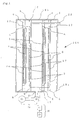
Fig. 1 is an explanatory view showing an overall structure of a plasma processing apparatus (thin-film forming apparatus) according to one embodiment of the present invention. -
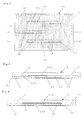
Fig. 2 is a bottom view of a cathode electrode constituting the plasma processing apparatus inFig. 1 . -
Fig. 3 is a sectional view taken along line A1 - A1 inFig. 2 . -
Fig. 4 is a sectional view taken along line A2 - A2 inFig. 2 . -
- 1
- Substrate
- 2
- Shower plate
- 3
- Back plate
- 4
- Anode electrode
- 5
- Second support member
- 6
- First support member
- 7
- Tray
- 10
- Plasma exciting power source
- 11
- Impedance matching box
- 12
- Cathode electrode
- 15
- Chamber (reaction chamber)
- 17
- Hollow room
- 18
- First gas-ejection hole
- 19
- Inner-wall of the hollow room
- 20
- Exhaust pipe
- 21
- Vacuum pump
- 22
- Pressure controller
- 24
- Heater
- 27
- Power introducing terminal
- 28
- Gas introducing section
- 29
- Exhaust section
- 30
- High-frequency power source section
- 31
- Gas introducing port
- 32
- Second gas-ejection hole
- 33
- Gas guiding section
- 33a
- Channel
- 33b
- Cover
- A plasma processing apparatus according to the present invention is used for forming a silicon thin film with a plasma CVD method, for example.
- Examples of the silicon thin film include a thin film from a crystalline thin film to an amorphous thin film having a silicon as a main component. A gas containing a silicon element can be used as a reactive gas. Specifically, a silane (SiH4), or disilane (Si2H6) can be used as the reactive gas, wherein these silane and disilane may be diluted with a hydrogen (H2), helium (He), or the like.
- Other examples of the silicon thin film formed by the plasma processing apparatus according to the present invention include a silicon carbide (SiC) film, a silicon nitride (SiN) film, a silicon oxide (SiO) film, an SiGe film, and the like.
- When a silicon carbide film is formed, a CH4 gas or C2H6 gas containing a carbon element is simultaneously introduced as a reactive gas in addition to a gas containing a silicon element. When a silicon nitride film is formed, an NH3 gas or NO gas containing a nitrogen element is simultaneously introduced as a reactive gas in addition to the gas containing a silicon element. When a silicon oxide film is formed, an NO gas or CO2 gas containing an oxygen element is simultaneously introduced as a reactive gas in addition to the gas containing a silicon element. When a SiGe film is formed, a GeH4 gas containing a germanium element is simultaneously introduced as a reactive gas in addition to the gas containing a silicon element.
- An impurity may be added to the silicon thin film in order to control conductivity. When the silicon thin film is made into an n-type, a PH3 gas containing an impurity element is simultaneously introduced, while when the silicon film is made into a p-type, a B2H6 gas containing an impurity element is simultaneously introduced.
- In the plasma processing apparatus according to the present invention, a chamber in which at least an interior can be evacuated can be used as the reaction chamber. Such a reaction chamber can be produced with, for example, stainless steel, an aluminum alloy, or the like. When the reaction chamber is made of two or more members, it is preferable that the chamber has a structure that can completely be sealed by using an O-ring at a fitting portion.
- In the plasma processing apparatus according to the present invention, examples of usable exhaust section include an exhaust section including a vacuum pump, an exhaust pipe that connects the reaction chamber and the vacuum pump, and a pressure controller provided midway on the exhaust pipe.
- In the plasma processing apparatus according to the present invention, a high-frequency power source section for applying high-frequency power between the cathode electrode and the anode electrode is provided. As the high-frequency power source section, for example, one composed of a plasma exciting power source and an impedance matching box can be used.
- In the plasma processing apparatus according to the present invention, one having a flat plate shape and made of a heat-resistant conductive material such as stainless steel, an aluminum alloy, carbon, or the like can be used as the cathode electrode and the anode electrode. A shape, size, and material of the cathode electrode and the anode electrode are preferably substantially equal, and when a residual processing strain is left due to a machining process, the residual processing strain is preferably removed by an annealing treatment.
- The used cathode electrode is provided with a hollow room provided therein, and a shower plate provided with plural first gas-ejection holes for ejecting a gas, which is introduced into the hollow room, from the hollow room to a portion between the cathode electrode and the anode electrode. According to need, an electrode-heating heater may be provided in the hollow room. The anode electrode has a hollow structure, for example, and an electrode-heating heater may be incorporated therein.
- In the plasma processing apparatus according to the present invention, a gas introducing port is provided at an end face of the cathode electrode of an inner-wall of the hollow room opposite to the shower plate. The gas introducing port is for introducing a gas into the hollow room from an outside of the cathode electrode.
- Plural second gas-ejection holes and a gas guiding section are provided at the inner-wall of the hollow room opposite to the shower plate. The second gas-ejection holes are for ejecting the gas into the hollow room, while the gas guiding section is for guiding the gas to the second gas-ejection holes from the gas introducing port.
- The gas guiding section may include, for example, a channel formed in the inner-wall of the hollow room opposite to the shower plate and a cover that covers the channel. The gas guiding section is not necessarily be configured to include such a channel, but may be configured to include holes formed on the inner-wall of the hollow room, for example.
- When the gas guiding section includes the channel formed in the inner-wall of the hollow room opposite to the shower plate and the cover that covers the channel, the gas guiding section can easily be formed in the inner-wall of the hollow room.
- The channel may be, for example, linear, curved, or formed by a combination of a linear portion and a curved portion. The cover can be constituted from, for example, a flat plate having a planar shape same as a planar shape of the channel.
- The second gas-ejection holes can be provided, for example, by opening through-holes in the cover. When the gas-ejection holes are provided by opening the through-holes in the cover, positions and diameters of the second gas-ejection holes can easily be changed (adjusted) by exchanging the cover.
- The second gas-ejection holes can be provided, for example, on the portion where the channel is not covered by the cover. When the second gas-ejection holes are provided on the portion where the channel is not covered by the cover, the positions and the diameters of the second gas-ejection holes can easily be changed (adjusted) by exchanging the cover.
- The second gas-ejection holes can be provided, for example, at a central part of the inner-wall of the hollow room opposite to the shower plate, and on a circumference of one circle or plural of circumferences of plural concentric circles about the central part. When the second gas-ejection holes are provided at such portions, a gas can more uniformly be supplied between the cathode electrode and the anode electrode, even when areas of the cathode electrode and the anode electrode are increased.
- The second gas-ejection holes, for example, are provided in such a manner that at least one hole is provided at the central part of the inner-wall of the hollow room opposite to the shower plate and plural holes are provided on a circumference of one circle about the central part in a point symmetric manner. When the second gas-ejection holes are provided in such number and at such portions, a gas can be supplied more uniformly and reliably between the cathode electrode and the anode electrode, even when the areas of the cathode electrode and the anode electrode are increased.
- It is preferable that an open area of the second gas-ejection hole provided on the central part of the inner-wall of the hollow room opposite to the shower plate is smaller than an open area of each of another second gas-ejection holes provided on one circumference of one circle or plural circumferences of plural concentric circles about the central part. When the open area of the second gas-ejection hole provided on the central part of the inner-wall of the hollow room opposite to the shower plate is smaller than the open area of each of another second gas-ejection holes provided on the circumference of one circle or plural circumferences of plural concentric circles about the central part, the gas at the central part of the cathode electrode is difficult to be exhausted when the areas of the cathode electrode and the anode electrode are increased, whereby the gas can more uniformly be supplied between the cathode electrode and the anode electrode.
- A plasma processing apparatus for forming a thin film according to one embodiment of the present invention will be described in detail with reference to
Figs. 1 to 4 . - As shown in
Fig. 1 , a thin-film formingplasma processing apparatus 100 has a chamber 15 serving as a reaction chamber for a plasma reaction, agas introducing port 28 for introducing a reaction gas into the chamber 15, anexhaust section 29 for exhausting the reactive gas in the chamber 15, and a high-frequencypower source section 30 for applying high-frequency power into the chamber 15. - Arranged in the chamber 15 are a rectangular flat-plate-
like anode electrode 4, a rectangular flat-plate-like cathode electrode 12, two sets of afirst support member 6 and asecond support member 5 for supporting therespective electrodes 4 and 12 at respective peripheral regions thereof. The cathode electrode 12 has ashower plate 2 and aback plate 3, and is arranged so as to be opposite to theanode electrode 4. - The chamber 15 is made of a main body and a door (not shown) provided at the front of the main body. The main body and the door can be made of stainless steel, an aluminum alloy, or the like. A fitting section of the main body and the door is sealed by using an O-ring (not shown).
- The
exhaust section 29 including anexhaust pipe 20, a vacuum pump 21, and apressure controller 22 is connected to the chamber 15 so as to be capable of controlling an inside of the chamber 15 to have an optional vacuum. - One
first support member 6 is provided in proximity to each corner of a rectangular bottom surface 15a and a rectangular top surface 15b of the main body of the chamber 15, wherein the respectivefirst support members 6 support theanode electrode 4. - The size of each of the
anode electrodes 4 is set to a suitable size according to a size of asubstrate 1 on which a film is to be formed. In the present embodiment, the size of thesubstrate 1 is set to be 900 × 550 mm, and a planar size of theanode electrode 4 according to thesubstrate 1 is set to be 1000 × 600 mm, and a thickness thereof is set to be 10 to 30 mm. - The
anode electrode 4 can be made of stainless steel, an aluminum alloy, carbon, or the like. In the present embodiment, theanode electrode 4 is made of an aluminum alloy. - The
anode electrode 4 has a hollow structure, wherein a heater (sheath heater) 24 is incorporated in a hollow portion thereof. Theanode electrode 4 has a residual processing strain left therein due to a machining process, which is performed to create the hollow structure. Therefore, theanode electrode 4 is subjected to an annealing treatment to remove the residual processing strain, before it is used. The annealing treatment is performed by using a closed-type temperature sensor such as a thermocouple. A treatment temperature in the annealing treatment is different depending upon a metal used as theanode electrode 4. When an aluminum alloy is used, there is generally employed a temperature cycle in which the aluminum alloy is kept to be 345°C, and then, slowly cooled. - The
anode electrode 4 is fixed to thefirst support member 6 with a screw. - The
anode electrode 4 and the chamber 15 are electrically connected with two ground plates. Specifically, the ground plate is made of an aluminum plate having a width of 10 to 35 mm and a thickness of 0.5 to 3 mm, and is attached to each of upper and lower end faces of theanode electrode 4. - Each of the cathode electrodes 12 includes a rectangular flat-plate-
like shower plate 2 and aback plate 3 that covers theshower plate 2 from back. Ahollow room 17 is provided between theshower plate 2 and theback plate 3. Theshower plate 2 and theback plate 3 can be made of stainless steel, an aluminum alloy, or the like, but it is preferable that they are made of a material substantially same as the material of theanode electrode 4. In the present embodiment, theshower plate 2 and theback plate 3 are made of an aluminum alloy. - A size of the cathode electrode 12 is set to a suitable size according to the size of the
substrate 1 on which a film is to be formed. In the present embodiment, a planar size of the cathode electrode 12 is set to be 1000 × 600 mm, and a thickness is set to be 20 to 30 mm, which are substantially equal to the size of theanode electrode 4. - As shown in
Figs. 2 to 4 , thehollow room 17 occupies about 95% of the planar area of the cathode electrode 12, and a height thereof (e.g., 8 mm) occupies about 30% of the thickness of the cathode electrode 12 (e.g., 25 mm). - Plural (several hundreds) first gas-ejection holes 18 are provided on substantially an entire surface of the
shower plate 2. Each of the gas-ejection holes 18 has a diameter of 0.1 mm, and are arranged in such a manner that an arrangement space (pitch) between the adjacent first gas-ejection holes 18 is 2.0 mm. These first gas-ejection holes 18 are for ejecting a gas, which is introduced into thehollow room 17, between the cathode electrode 12 and theanode electrode 4 from thehollow room 17. - As shown in
Fig. 3 , a lower surface of theback plate 3 of the cathode electrode 12 also serves as a ceiling surface of thehollow room 17, and it is sometimes referred to herein as a inner-wall 19 of thehollow room 17 opposite to theshower plate 2. - A gas introducing port 31 for introducing a gas from an outside of the cathode electrode 12 is provided at one of the electrode end face of the inner-
wall 19 of thehollow room 17 opposite to theshower plate 2. Further, the inner-wall 19 of thehollow room 17 opposite to theshower plate 2 is provided with five second gas-ejection holes 32 for ejecting the gas into thehollow room 17 and agas guide section 33 for guiding the gas to these second gas-ejection holes 32. - As shown in
Fig. 2 , the five second gas-ejection holes 32 are provided in such a manner that one second gas-ejection hole is provided at a center of the inner-wall 19 of thehollow room 17 opposite to theshower plate 2, and four second gas-ejection holes are provided on a circumference of one circle around the center in a point symmetric manner. - The
gas guide section 33 includes a channel 33a formed on the inner-wall 19 of thehollow room 17 opposite to theshower plate 2 and a cover 33b that covers the channel 33a. - As shown in
Fig. 2 , the channel 33a has an H-shaped section that has an H-shaped planar shape and is formed on the central part of the inner-wall 19 of thehollow room 17, and an I-shaped section that has one end communicating with the gas introducing port 31 and the other end communicating with a central part of the H-shaped section. A length of the H-shaped section in a direction of a long side is set to be 600 mm, while a length of the I-shaped section in a direction of a long side is set to be 480 mm. The channel 33a has a rectangular cross section, and is set to have a width of 20 mm and a depth of 2 mm. - The cover 33b includes an H-shaped section and an I-shaped section corresponding to the above planar shape of the channel 33a. The cover 33b is made of a material same as that of the cathode electrode 12, and is set to have a width of 30 mm and a thickness of 1 mm. The cover 33b is fixed to an opening peripheral edge of the channel 33a of the inner-
wall 19 of thehollow room 17 with a screw. - As shown in
Figs. 2 to 4 , in the five second gas-ejection holes 32, the one second gas-ejection hole 32, which is provided at the center of the inner-wall 19 of thehollow room 17, is open at the central part of the H-shaped section of the channel 33a, while the four second gas-ejection holes 32 provided on one circumference in a point symmetric manner are open at the respective four corners of the H-shaped section of the channel 33a. - A diameter of the one second gas-ejection hole 32 is 1.5 mm, and a diameter of each of the four second gas-ejection holes 32 is 2.0 mm. Accordingly, the open area of the one second gas-ejection hole 32 is set to be smaller than the respective open areas of the four second gas-ejection holes 32.
- As shown in
Figs. 2 and 3 , the gas introducing port 31 of the cathode electrode 12 communicates with one end of the I-shaped section of the channel 33a. A reactive gas introduced from thegas introducing section 28 shown inFig. 1 into thehollow room 17 through the gas introducing port 31 of the cathode electrode 12, the I-shaped section and the H-shaped section of the channel 33a, and the five second gas-ejection holes 32 is ejected like a shower between the cathode electrode 12 and theanode electrode 4 from several hundreds of first gas-ejection holes 18 formed on theshower plate 2 of the cathode electrode 12. - Similar to the
anode electrode 4, a residual processing strain caused by a machining process is also left in theshower plate 2 and theback plate 3 of the cathode electrode 12. Therefore, before the cathode electrode 12 is used, an annealing treatment is performed to remove the residual processing strain. A treatment temperature in the annealing treatment is different depending upon a metal used as theshower plate 2 and theback plate 3. When an aluminum alloy is used, there is generally employed a temperature cycle in which the aluminum alloy is kept to be 345°C, and then, slowly cooled. - As shown in
Fig. 1 , two sets of the cathode electrodes 12 are supported on a total of eightsecond support members 5, which are provided on the rectangular bottom surface 15a and the rectangular top surface 15b of the main body of the chamber 15. Each of thesecond support members 5 can be made of glass, alumina, or zirconia, or the like, and in this embodiment, alumina or zirconia is used. - The respective cathode electrodes 12 are fixed on the
second support members 5 with screws. - A high-frequency
power source section 30 including a plasmaexciting power source 10 and animpedance matching box 11 is connected to the respective cathode electrodes 12 through apower introducing terminal 27 so as to apply high-frequency power. The plasmaexciting power source 10 uses power of 10 W to 100 kW with a frequency of DC to 108.48 MHz. In the present embodiment, power of 10 W to 100 kW with a frequency of 1 MHz to 54.24 MHz is used. - A reactive gas composed of SiH, which is diluted with H2, is introduced into the thin-film forming
plasma processing apparatus 100 having the above-mentioned configuration with a predetermined flow rate and a predetermined pressure through the cathode electrode 12, and the high-frequency power is applied between the cathode electrode 12 and theanode electrode 4 to produce a glow discharge. Accordingly, a silicon thin film with a thickness of 300 nm is deposited onto thesubstrate 1 for a film forming time of 10 minutes with a thickness distribution of less than and equal to ±10%. - Although the
plasma processing apparatus 100 has a two-stage structure in the present embodiment, a structure of three or more stages is possible in another plasma processing apparatus by repeating similar structures.
Claims (8)
- A plasma processing apparatus comprising: a reaction chamber for a plasma reaction; an exhaust section for exhausting a gas from the reaction chamber; and a flat-plate-like cathode electrode and a flat-plate-like anode electrode arranged in the reaction chamber so as to be opposite to each other, wherein
plural sets of the cathode electrode and the anode electrode are arranged in opposing directions thereof,
each of the cathode electrodes includes a hollow room therein, and a shower plate provided with plural first gas-ejection holes for ejecting the gas, which is introduced into the hollow room, from the hollow room to a portion between the cathode electrode and the anode electrode,
a gas introducing port for introducing the gas from an outside of the cathode electrode is provided at an electrode end face of an inner-wall of the hollow room opposite to the shower plate at the cathode electrode, and
plural second gas-ejection holes for ejecting the gas into the hollow room and a gas guiding section for guiding the gas from the gas introducing port to the second gas-ejection holes are provided at the inner-wall of the hollow room opposite to the shower plate. - The plasma processing apparatus according to claim 1, wherein
the gas guiding section includes a channel formed on the inner-wall of the hollow room opposite to the shower plate, and a cover that covers the channel. - The plasma processing apparatus according to claim 2, wherein
the cover is a flat plate. - The plasma processing apparatus according to claim 2 or 3, wherein
the second gas-ejection holes are provided by opening through-holes in the cover. - The plasma processing apparatus according to claim 2 or 3, wherein
the second gas-ejection holes are provided on a portion where the channel is not covered by the cover. - The plasma processing apparatus according to any one of claims 1 to 5, wherein
the second gas-ejection holes are provided on a central part of the inner-wall of the hollow room opposite to the shower plate and on a circumference of one circle or plural circumferences of plural concentric circles about the central part. - The plasma processing apparatus according to any one of claims 1 to 6, wherein
the second gas-ejection holes are provided in such a manner that at least one hole is provided at the central part of the inner-wall of the hollow room opposite to the shower plate and plural holes are provided on the circumference of one circle about the central part in a point symmetric manner. - The plasma processing apparatus according to claim 6 or 7, wherein
an open area of each of the second gas-ejection holes provided on the central part of the inner-wall of the hollow room opposite to the shower plate is smaller than an open area of each of another second gas-ejection holes provided on one circumference of one circle or plural circumferences of plural concentric circles about the central part.
Applications Claiming Priority (2)
| Application Number | Priority Date | Filing Date | Title |
|---|---|---|---|
| JP2008004600A JP5039576B2 (en) | 2008-01-11 | 2008-01-11 | Plasma processing equipment |
| PCT/JP2008/073227 WO2009087887A1 (en) | 2008-01-11 | 2008-12-19 | Plasma processing apparatus |
Publications (2)
| Publication Number | Publication Date |
|---|---|
| EP2241651A1 true EP2241651A1 (en) | 2010-10-20 |
| EP2241651A4 EP2241651A4 (en) | 2012-12-05 |
Family
ID=40853011
Family Applications (1)
| Application Number | Title | Priority Date | Filing Date |
|---|---|---|---|
| EP08869403A Withdrawn EP2241651A4 (en) | 2008-01-11 | 2008-12-19 | PLASMA TREATMENT APPARATUS |
Country Status (6)
| Country | Link |
|---|---|
| US (1) | US20100277050A1 (en) |
| EP (1) | EP2241651A4 (en) |
| JP (1) | JP5039576B2 (en) |
| KR (1) | KR101224669B1 (en) |
| CN (1) | CN101910460A (en) |
| WO (1) | WO2009087887A1 (en) |
Families Citing this family (7)
| Publication number | Priority date | Publication date | Assignee | Title |
|---|---|---|---|---|
| KR101100284B1 (en) * | 2010-06-21 | 2011-12-30 | 세메스 주식회사 | Thin film deposition apparatus |
| US20110308458A1 (en) * | 2010-06-21 | 2011-12-22 | Semes Co., Ltd. | Thin Film Deposition Apparatus |
| TWI427183B (en) * | 2010-11-25 | 2014-02-21 | Ind Tech Res Inst | Plasma processing apparatus |
| KR20140036765A (en) | 2012-09-18 | 2014-03-26 | 삼성디스플레이 주식회사 | Sputtring device |
| US10984987B2 (en) | 2018-10-10 | 2021-04-20 | Lam Research Corporation | Showerhead faceplate having flow apertures configured for hollow cathode discharge suppression |
| CN112619334A (en) * | 2020-10-22 | 2021-04-09 | 无锡英普朗科技有限公司 | High-temperature plasma reaction device |
| CN116555920B (en) * | 2023-06-27 | 2024-01-23 | 通威微电子有限公司 | Silicon carbide seed crystal bonding method |
Family Cites Families (14)
| Publication number | Priority date | Publication date | Assignee | Title |
|---|---|---|---|---|
| US5882411A (en) * | 1996-10-21 | 1999-03-16 | Applied Materials, Inc. | Faceplate thermal choke in a CVD plasma reactor |
| JPH10223620A (en) * | 1997-02-06 | 1998-08-21 | Hitachi Ltd | Semiconductor manufacturing equipment |
| JP3386986B2 (en) * | 1997-10-16 | 2003-03-17 | シャープ株式会社 | Plasma processing equipment |
| JP2001244256A (en) * | 2000-03-02 | 2001-09-07 | Hitachi Ltd | Processing equipment |
| DE10045958B4 (en) * | 2000-09-16 | 2008-12-04 | Muegge Electronic Gmbh | Device for conducting a gaseous medium into and / or out of a process chamber |
| JP4454621B2 (en) * | 2001-01-22 | 2010-04-21 | 東京エレクトロン株式会社 | Processing equipment |
| KR100756107B1 (en) * | 2001-02-09 | 2007-09-05 | 동경 엘렉트론 주식회사 | Deposition device |
| JP2004288984A (en) * | 2003-03-24 | 2004-10-14 | Sharp Corp | Film forming apparatus and film forming method |
| JP4770167B2 (en) * | 2004-12-16 | 2011-09-14 | 株式会社島津製作所 | Film forming method using surface wave excitation plasma CVD apparatus |
| JP4584722B2 (en) * | 2005-01-13 | 2010-11-24 | シャープ株式会社 | Plasma processing apparatus and semiconductor device manufactured by the same |
| JP2006196681A (en) * | 2005-01-13 | 2006-07-27 | Sharp Corp | Plasma processing apparatus and semiconductor device manufactured by the same |
| JP2006299294A (en) * | 2005-04-15 | 2006-11-02 | Tokyo Electron Ltd | Gas supply apparatus and film forming apparatus |
| JP4517935B2 (en) | 2005-05-19 | 2010-08-04 | 株式会社島津製作所 | Shower plate and surface wave excitation plasma processing apparatus |
| JP4916220B2 (en) * | 2006-05-31 | 2012-04-11 | 東京エレクトロン株式会社 | Plasma processing apparatus and electrodes used therefor |
-
2008
- 2008-01-11 JP JP2008004600A patent/JP5039576B2/en not_active Expired - Fee Related
- 2008-12-19 WO PCT/JP2008/073227 patent/WO2009087887A1/en not_active Ceased
- 2008-12-19 KR KR1020107015226A patent/KR101224669B1/en not_active Expired - Fee Related
- 2008-12-19 US US12/811,753 patent/US20100277050A1/en not_active Abandoned
- 2008-12-19 EP EP08869403A patent/EP2241651A4/en not_active Withdrawn
- 2008-12-19 CN CN200880124530XA patent/CN101910460A/en active Pending
Also Published As
| Publication number | Publication date |
|---|---|
| US20100277050A1 (en) | 2010-11-04 |
| KR101224669B1 (en) | 2013-01-21 |
| WO2009087887A1 (en) | 2009-07-16 |
| JP5039576B2 (en) | 2012-10-03 |
| KR20100093109A (en) | 2010-08-24 |
| JP2009167445A (en) | 2009-07-30 |
| CN101910460A (en) | 2010-12-08 |
| EP2241651A4 (en) | 2012-12-05 |
Similar Documents
| Publication | Publication Date | Title |
|---|---|---|
| EP2241651A1 (en) | Plasma processing apparatus | |
| KR101236108B1 (en) | Substrate processing apparatus and method of manufacturing semiconductor device | |
| TWI744229B (en) | Wafer boat, treatment apparatus for wafers and treatment method for wafers | |
| CN100390943C (en) | Thin-film shaper and shaping method thereof | |
| TWI500809B (en) | Plasma CVD device and method for manufacturing ruthenium film | |
| WO2003096400A1 (en) | Plasma processing equipment and plasma processing method | |
| WO2007145230A1 (en) | Shower plate, plasma processing apparatus using the same, plasma processing method, and method for manufacturing electronic device | |
| US8092640B2 (en) | Plasma processing apparatus and semiconductor device manufactured by the same apparatus | |
| US20010030024A1 (en) | Plasma-enhanced processing apparatus | |
| US7032536B2 (en) | Thin film formation apparatus including engagement members for support during thermal expansion | |
| EP1650326A2 (en) | Plasma processing apparatus | |
| KR20180014656A (en) | Substrate processing apparatus and substrate processing method | |
| EP2282619A1 (en) | Plasma processing apparatus | |
| US7722738B2 (en) | Semiconductor device manufacturing unit and semiconductor device manufacturing method | |
| WO2010079766A1 (en) | Plasma processing apparatus | |
| CN1334885A (en) | Large area plasma source | |
| JP4936297B2 (en) | Plasma processing apparatus, plasma processing method, and semiconductor device | |
| US8093142B2 (en) | Plasma processing apparatus and plasma processing method | |
| US8931433B2 (en) | Plasma processing apparatus | |
| US20250022694A1 (en) | Heater plates with distributed purge channels, rf meshes and ground electrodes | |
| JP2003273094A (en) | CVD apparatus and method for performing post-processing step after film formation in CVD apparatus | |
| JP2004149917A (en) | Thin film manufacturing apparatus and thin film manufacturing method using the apparatus | |
| CN117358713A (en) | Cleaning device and cleaning method for process substrate carrier |
Legal Events
| Date | Code | Title | Description |
|---|---|---|---|
| PUAI | Public reference made under article 153(3) epc to a published international application that has entered the european phase |
Free format text: ORIGINAL CODE: 0009012 |
|
| 17P | Request for examination filed |
Effective date: 20100719 |
|
| AK | Designated contracting states |
Kind code of ref document: A1 Designated state(s): AT BE BG CH CY CZ DE DK EE ES FI FR GB GR HR HU IE IS IT LI LT LU LV MC MT NL NO PL PT RO SE SI SK TR |
|
| AX | Request for extension of the european patent |
Extension state: AL BA MK RS |
|
| DAX | Request for extension of the european patent (deleted) | ||
| A4 | Supplementary search report drawn up and despatched |
Effective date: 20121106 |
|
| RIC1 | Information provided on ipc code assigned before grant |
Ipc: H01J 37/32 20060101ALI20121030BHEP Ipc: C23C 16/455 20060101AFI20121030BHEP Ipc: H01L 21/205 20060101ALI20121030BHEP Ipc: H05H 1/46 20060101ALI20121030BHEP Ipc: C23C 16/509 20060101ALI20121030BHEP |
|
| GRAP | Despatch of communication of intention to grant a patent |
Free format text: ORIGINAL CODE: EPIDOSNIGR1 |
|
| RIC1 | Information provided on ipc code assigned before grant |
Ipc: C23C 16/509 20060101ALI20140506BHEP Ipc: H01L 21/02 20060101ALI20140506BHEP Ipc: C23C 16/455 20060101AFI20140506BHEP Ipc: H01L 21/205 20060101ALI20140506BHEP Ipc: H05H 1/46 20060101ALI20140506BHEP Ipc: H01J 37/32 20060101ALI20140506BHEP |
|
| INTG | Intention to grant announced |
Effective date: 20140521 |
|
| STAA | Information on the status of an ep patent application or granted ep patent |
Free format text: STATUS: THE APPLICATION IS DEEMED TO BE WITHDRAWN |
|
| 18D | Application deemed to be withdrawn |
Effective date: 20141001 |