EP2239845A1 - MEMS resonator - Google Patents
MEMS resonator Download PDFInfo
- Publication number
- EP2239845A1 EP2239845A1 EP09100232A EP09100232A EP2239845A1 EP 2239845 A1 EP2239845 A1 EP 2239845A1 EP 09100232 A EP09100232 A EP 09100232A EP 09100232 A EP09100232 A EP 09100232A EP 2239845 A1 EP2239845 A1 EP 2239845A1
- Authority
- EP
- European Patent Office
- Prior art keywords
- resonator
- layout
- variation
- frequency
- physical
- Prior art date
- Legal status (The legal status is an assumption and is not a legal conclusion. Google has not performed a legal analysis and makes no representation as to the accuracy of the status listed.)
- Withdrawn
Links
- 238000000034 method Methods 0.000 claims abstract description 27
- 238000012986 modification Methods 0.000 claims abstract description 20
- 230000004048 modification Effects 0.000 claims abstract description 20
- 239000000725 suspension Substances 0.000 claims description 14
- 238000013461 design Methods 0.000 abstract description 49
- 230000008569 process Effects 0.000 abstract description 13
- 230000000694 effects Effects 0.000 abstract description 6
- 238000004088 simulation Methods 0.000 description 10
- 230000008859 change Effects 0.000 description 9
- 239000000463 material Substances 0.000 description 9
- XUIMIQQOPSSXEZ-UHFFFAOYSA-N Silicon Chemical compound [Si] XUIMIQQOPSSXEZ-UHFFFAOYSA-N 0.000 description 6
- 239000000758 substrate Substances 0.000 description 6
- 238000005259 measurement Methods 0.000 description 5
- 229910052710 silicon Inorganic materials 0.000 description 5
- 239000010703 silicon Substances 0.000 description 5
- 238000012545 processing Methods 0.000 description 4
- 230000009897 systematic effect Effects 0.000 description 4
- 238000012546 transfer Methods 0.000 description 4
- 235000012431 wafers Nutrition 0.000 description 4
- 230000001419 dependent effect Effects 0.000 description 3
- 238000001459 lithography Methods 0.000 description 3
- 238000004519 manufacturing process Methods 0.000 description 3
- 238000009966 trimming Methods 0.000 description 3
- 238000013459 approach Methods 0.000 description 2
- 230000007423 decrease Effects 0.000 description 2
- 239000012212 insulator Substances 0.000 description 2
- 238000005459 micromachining Methods 0.000 description 2
- 230000001902 propagating effect Effects 0.000 description 2
- 238000010923 batch production Methods 0.000 description 1
- 239000003990 capacitor Substances 0.000 description 1
- 230000006835 compression Effects 0.000 description 1
- 238000007906 compression Methods 0.000 description 1
- 238000006073 displacement reaction Methods 0.000 description 1
- 238000004146 energy storage Methods 0.000 description 1
- 238000002474 experimental method Methods 0.000 description 1
- 230000002349 favourable effect Effects 0.000 description 1
- 239000012530 fluid Substances 0.000 description 1
- 230000010354 integration Effects 0.000 description 1
- 230000001788 irregular Effects 0.000 description 1
- 238000005457 optimization Methods 0.000 description 1
- 229920002120 photoresistant polymer Polymers 0.000 description 1
- 239000010453 quartz Substances 0.000 description 1
- 230000004044 response Effects 0.000 description 1
- VYPSYNLAJGMNEJ-UHFFFAOYSA-N silicon dioxide Inorganic materials O=[Si]=O VYPSYNLAJGMNEJ-UHFFFAOYSA-N 0.000 description 1
- 238000005549 size reduction Methods 0.000 description 1
- 230000007704 transition Effects 0.000 description 1
Images




Classifications
-
- H—ELECTRICITY
- H03—ELECTRONIC CIRCUITRY
- H03H—IMPEDANCE NETWORKS, e.g. RESONANT CIRCUITS; RESONATORS
- H03H3/00—Apparatus or processes specially adapted for the manufacture of impedance networks, resonating circuits, resonators
- H03H3/007—Apparatus or processes specially adapted for the manufacture of impedance networks, resonating circuits, resonators for the manufacture of electromechanical resonators or networks
- H03H3/0072—Apparatus or processes specially adapted for the manufacture of impedance networks, resonating circuits, resonators for the manufacture of electromechanical resonators or networks of microelectro-mechanical resonators or networks
- H03H3/0076—Apparatus or processes specially adapted for the manufacture of impedance networks, resonating circuits, resonators for the manufacture of electromechanical resonators or networks of microelectro-mechanical resonators or networks for obtaining desired frequency or temperature coefficients
-
- H—ELECTRICITY
- H03—ELECTRONIC CIRCUITRY
- H03H—IMPEDANCE NETWORKS, e.g. RESONANT CIRCUITS; RESONATORS
- H03H9/00—Networks comprising electromechanical or electro-acoustic elements; Electromechanical resonators
- H03H9/24—Constructional features of resonators of material which is not piezoelectric, electrostrictive, or magnetostrictive
- H03H9/2405—Constructional features of resonators of material which is not piezoelectric, electrostrictive, or magnetostrictive of microelectro-mechanical resonators
-
- H—ELECTRICITY
- H03—ELECTRONIC CIRCUITRY
- H03H—IMPEDANCE NETWORKS, e.g. RESONANT CIRCUITS; RESONATORS
- H03H9/00—Networks comprising electromechanical or electro-acoustic elements; Electromechanical resonators
- H03H9/24—Constructional features of resonators of material which is not piezoelectric, electrostrictive, or magnetostrictive
- H03H9/2405—Constructional features of resonators of material which is not piezoelectric, electrostrictive, or magnetostrictive of microelectro-mechanical resonators
- H03H9/2447—Beam resonators
- H03H9/2457—Clamped-free beam resonators
-
- H—ELECTRICITY
- H03—ELECTRONIC CIRCUITRY
- H03H—IMPEDANCE NETWORKS, e.g. RESONANT CIRCUITS; RESONATORS
- H03H9/00—Networks comprising electromechanical or electro-acoustic elements; Electromechanical resonators
- H03H9/02—Details
- H03H9/02244—Details of microelectro-mechanical resonators
- H03H2009/02488—Vibration modes
- H03H2009/02496—Horizontal, i.e. parallel to the substrate plane
-
- H—ELECTRICITY
- H03—ELECTRONIC CIRCUITRY
- H03H—IMPEDANCE NETWORKS, e.g. RESONANT CIRCUITS; RESONATORS
- H03H9/00—Networks comprising electromechanical or electro-acoustic elements; Electromechanical resonators
- H03H9/02—Details
- H03H9/02244—Details of microelectro-mechanical resonators
- H03H2009/02488—Vibration modes
- H03H2009/02496—Horizontal, i.e. parallel to the substrate plane
- H03H2009/02503—Breath-like, e.g. Lam? mode, wine-glass mode
Definitions
- This invention relates to micro-electromechanical systems (MEMS). More particularly, it relates to MEMS resonator devices.
- MEMS resonators allow the integration of accurate timing and frequency reference devices on a silicon chip. This allows major cost and size reductions compared, for example, to conventional quartz oscillator circuits.
- Two existing designs for making a MEMS resonator are the square-extensional and the disk resonator.
- the most interesting resonance modes in these resonators are the extensional, or longitudinal, modes. These modes are favourable because they can store more energy than most flexural modes, and are therefore less susceptible to non-linearity.
- Extensional-mode - also known as planar-mode - vibration consists of a compression wave in the plane of the material. That is, the physical displacement of the material takes place in directions lying in the same plane as the resonator, alternately stretching and compressing the material.
- a resonator using this extensional mode, and in which the resonance frequency is determined by a sound wave propagating through the material, is generally known as a bulk acoustic mode resonator.
- FIG. 1 A typical processing sequence for the fabrication of a MEMS resonator is shown in Figure 1 .
- the resonator is surface micromachined into a 1.5 ⁇ m thick silicon on insulator substrate.
- Figure 1 a shows a mask pattern exposed and developed in photoresist 1 on top of the silicon on insulator structure 2.
- Figure 1b shows the resist pattern etched into the substrate to form cavities 4.
- a sacrificial layer 6 forming part of the substrate structure is etched to release the resonating beam.
- layout deviations are introduced due to non-perfect pattern transfer. For example, under etch occurs as is indicated by the arrows in Figure 1 b.
- This process can be implemented with standard CMOS processing tools, so that these resonators allow for batch production.
- the resonator dimensions are determined by the layout that is patterned on the mask. This mask pattern is then etched into the substrate.
- frequency accuracy is a key specification. For mid-end applications an accuracy of about 150 ppm, or even 100 ppm is required.
- the mechanical resonance frequency of the resonating element should thus be controlled with high precision.
- the main cause of resonator dimension inaccuracy is the non-perfect pattern transfer from the mask layout to the substrate. This is typically called under-etch or over-etch and results in geometric offset.
- This invention relates to measures for providing tolerance to this geometric offset.
- a bulk-acoustic-mode MEMS resonator comprising a resonator body having a first portion with a first physical layout, and a layout modification feature, wherein the resonant frequency is a function of the physical layout of the first portion and the physical layout of the layout modification feature, wherein the physical layouts are designed such that the frequency variation is less than 150ppm for a variation in edge position of the resonator shape edges of 50nm.
- This design combines at least two different layout features in such a way that small edge position variations (resulting from uncontrollable process variation) have negligible effect on the resonant frequency.
- variations in sound velocity compensate for variations in wavelength (these depend on the physical layout), and this in turn maintains a constant resonant frequency. This makes the resonance frequency insensitive to geometric offset due to process spread.
- the first derivative of resonant frequency with respect to the edge position variation is preferably substantially zero. This is sufficient to provide the resonant frequency within desired tolerance limits.
- the layout modification feature and the first portion can for example have different lateral cross-sections along the principal vibration direction. These different cross sections give rise to a reflection interface, so that the different portions each give rise to a respective standing wave, and the way these interact vary with physical layout changes.
- the layout modification feature can comprise holes or slits within the first portion.
- the holes or slits preferably have a dimension smaller than the acoustic wavelength. The way the holes or slits vary in response to process variations compared to the overall resonator shape gives rise to the compensation for the effect of geometric offset on the resonant frequency.
- the resonant vibration can be in a one-directional or two-directional mode.
- the resonator preferably further comprises external suspension springs, and an actuation arrangement can be provided which uses electrostatic actuation or thermal actuation.
- a readout arrangement can use capacitive readout, piezoresistive readout or piezoelectric readout.
- the invention also provides a method of designing a bulk-acoustic-mode MEMS resonator, comprising; designing a resonator body having a first portion with a first physical layout, and a layout modification feature; modeling the resonant frequency, taking into account the physical layout of the first portion and the physical layout of the layout modification feature, selecting the physical layouts such that the frequency variation is less than a first threshold (e.g. 150ppm) for a variation in edge position of the resonator shape edges of a second threshold (e.g. 50nm).
- a first threshold e.g. 150ppm
- a second threshold e.g. 50nm
- This design method enables frequency variations to be avoided based on the physical design of the resonator body.
- the modeling can be carried out using finite element analysis.
- the layout modification feature comprises holes or slits within the first portion, and wherein the modeling takes into account the hole or slit dimensions and positions, the first portion dimensions and any suspension system for the resonator body.
- the layout modification feature comprises a portion of different lateral cross-section along a principal vibration direction to the first portion, and wherein the modeling takes into account the lateral cross sections and dimensions of the first portion and the layout modification feature, and any suspension system for the resonator body.
- Fig. 2 shows a typical square MEMS resonator apparatus according to the prior art to show how the device operates.
- the resonator 10 is suspended between a set of electrodes 12.
- the electrodes are all actuation electrodes applying an input signal V in to the resonator 10.
- the resonator is suspended at its corners.
- Output measurement is achieved using connection contact 14 at one corner, which is electrically connected to the bulk of the resonator.
- Application of an input signal V in to the electrodes 12 exerts electrostatic force on the resonator plate 10.
- the electrodes and plate form a capacitor. Any movement of the plate relative to the electrodes will change the capacitance across the gap. This is precisely what occurs at resonance - the electrostatic forces generated by the AC input signal generate a resonance of the mechanical structure. This results in a capacitance change, which produces an output voltage V out which is directly related to the time-varying capacitance.
- This invention relates to measures for providing tolerance to geometric offset. This has been considered for flex-mode resonators.
- the resonance frequency of a mechanical resonator depends on its effective stiffness and mass.
- a mechanical resonator can be modeled by a mass m, spring k and damper system ⁇ .
- This invention relates specifically to bulk acoustic mode resonators and aims to provide designs which are insensitive to geometric offset for this type of resonator.
- Bulk-acoustic resonators are much stiffer then flex-mode resonators. Therefore, they can be scaled to much higher frequencies than traditional flex-mode designs. Moreover, the stiffer bulk-acoustic resonator is able to store more energy, which improves phase noise performance.
- the relative change in wave velocity (v) is equal to the relative change in wavelength ( ⁇ ).
- this principle is applied to both one-directional and two-directional bulk-acoustic resonators.
- a standing wave of a quarter wavelength (fixed-free) or half wavelength (free-free) propagates in the material. These waves are continuous waves in the material rather than small lattice vibrations. As well as the fundamental mode, the principle also holds for higher order modes.
- Lithography and non-accurate pattern transfer account for the majority of micro-machining variations. Although these variations are temporally random, they are spatially systematic. The inaccuracy can thus be modelled as a systematic geometric offset ⁇ that accounts for the variability in resonator dimensions.
- This geometric offset represents the variation in edge position of the resonator shape edges between different samples created by a given process. This geometric offset is process dependent and is more or less fixed. This means that the offset has a larger effect on smaller structures.
- the main cause of geometric offset is non-accurate pattern transfer.
- the trenches and holes that need to be etched in the silicon layer are patterned in the resist by lithography.
- the pattern is transferred to the silicon ( Figure 1 b) , under or over etch occurs.
- wider trenches and holes can be formed as shown in Figure 1b , which mean that the actual silicon structure shaped by these trenches is smaller.
- the under and over etch affect the holes and trenches that shape the structure.
- Figure 3 also shows a square hole 20 of intended size (solid line) and size resulting from the offset (dotted line).
- the resonance frequency is determined by the length of the square.
- the velocity of sound is determined by the material constants; Youngs modulus E and density p.
- the first eigenmode is observed when the square length L equals half of the bulk-acoustic wavelength ⁇ .
- the scaling of the resonance frequency with plate dimensions is indicated in Figure 4 , which relates to a bulk-acoustic, square-plate resonator with plate length L.
- the resonance frequency is measured for five square-plate resonators for which plate length L is reduced by a factor 2 in every step.
- the resonance frequency will spread.
- a geometric offset of ⁇ 20 nm can easily result in 1000 ppm frequency spread. If the size of the square plate decreases, the total frequency spread increases.
- Holes in the plate affect the velocity of the bulk-acoustic-wave through the material.
- the holes are square shaped. The principle, however, holds for all shapes, so for example circles, triangles, crosses, slits can also be used.
- the velocity of the wave is reduced by the holes. If the size of the holes increases, the wave velocity is reduced further. For a square-plate with holes the wave velocity has also become dependant on geometric offset and is no longer constant.
- the square-plate resonator is typically suspended at its four corners. These corner suspensions act as springs.
- Figure 5 shows a square plate resonator with a single T-shaped corner-suspension (although suspensions will be provided at each corner).
- the main body is provided with an array of square holes.
- FEM simulations can be used to find designs that are insensitive to geometric offset. For the square-plate with square holes and T-shaped corner suspension in Figure 5 , such a design has been made at 52 MHz.
- This compensated design has been simulated, using three designs that have been given a geometric offset of -100, -50, and +50 nm respectively.
- Figure 6a shows the simulated (plot 60 "-") and measured (plot 62 " ⁇ ") frequency dependence on the geometric offset ⁇ .
- the plot 62 in Figure 6a shows measured data.
- An 8 inch wafer containing about 140 identical fields was fabricated. In each field, the 4 resonators were formed. In 80 fields, the 4 resonators were successfully measured and the graph shows the average frequency of these 80 measurements for each of the 4 resonators.
- the process variation is expected to be less than 150nm, for a size of resonator of between 50 and 400 ⁇ m.
- a histogram of the compensated design is plotted. For the 80 measured resonators on the wafer more than 90% of the measured resonators are within ⁇ 150 ppm of the average frequency. The dominant source of the measured frequency spread in the histogram is no longer caused by the geometric offset.
- FEM finite-element-simulation
- Figures 7a and 7b show the results of FEM simulation on compensated square plate designs as indicated in Figure 5 . All these designs are insensitive to geometric offset.
- the optimal hole pitch is shown for resonators of increased size L for hole size 0.5 ⁇ m (plot " ⁇ ") and hole size 1.1 ⁇ m (plot " ⁇ ").
- the square plate design is a two-directional, bulk-acoustic resonator.
- the compensation principle also holds for one-directional, bulk-acoustic resonators.
- the same method as for two-directional, bulk-acoustic resonators can be used.
- the acoustic wavelength is already dependent on geometric offset.
- the wave velocity again becomes dependent on geometric offset.
- an optimized pitch can be found that makes the structure insensitive to geometric offset. Again, this holds for holes of all shapes and sizes.
- the holes can be placed in an equidistant pattern or randomly over the structure.
- the structure has a non-uniform cross-section, the acoustic wave will show a phase jump over this boundary.
- the standing wave in the structure is composed of multiple standing waves with different wavelengths. This is most easily explained with reference to a one-directional, bulk-acoustic resonator.
- a resonator with uniform thickness and only one step change in width is shown in Figure 9a .
- This resonator has an effective bulk-acoustic-wavelength that depends on the geometric dimensions of both parts. This is thus a function of four variables that all depend on the geometric offset. Finding the parameters L 1 , W 1 , L 2 , and W 2 for which the derivative to the geometric offset of this function is zero can optimize the design. To improve the design further, the second-order derivative can also be made zero.
- This method can also work for two-directional devices, but examples are less straightforward to give.
- One example could be a square plate design that has a non-uniform layer thickness.
- a wave hits a physical boundary, part will be transmitted and part will be reflected.
- this is analogous to a wave in a fluid that crosses a boundary in depth, or light hitting a prism.
- the standing wave in the structure is composed of two parts of different wavelength that connect at the boundary. Over this boundary, the composed standing wave shows a discontinuity in phase.
- An abrupt transition of width can be used, but also a sloped boundary (e.g. a linearly increasing width) can also be considered.
- a standing wave is required in each portion.
- the design needs to be robust and needs to be processed with high precision.
- minimum and maximum widths should be set, for example 200 nm and 200 ⁇ s.
- Figure 9 shows three further examples of one-directional, bulk-acoustic resonators that are insensitive to geometric offset. All resonators vibrate in a longitudinal mode. An optimized design can use holes as explained for the square plate resonator. An example of this is the resonator in Figure 9d . However, as explained above, a width variation along the vibration direction of the structure can also make the resonator insensitive to geometric offset. Examples are shown in Figures 9a to 9c .
- Figure 9a shows a design which simply uses a width variation.
- Figure 9b shows a design which combines a width variation with holes in the wider part and a slot in the narrower part.
- Figure 9c shows a design which has constant width but uses a slot instead of an array of holes.
- Figure 10 shows FEM simulations for optimized one-directional ( Figure 9a ) and two-directional ( Figure 9b ) bulk-acoustic resonators. For a geometric offset range of ⁇ 50 nm, frequency spread is reduced to only a few ppm.
- Bulk-acoustic resonators are preferred over flex-mode resonators, because of their increased effective stiffness. This is important for:
- the MEMS resonators can be processed on 1.5 ⁇ m thick SOI wafers. These SOI wafers are available with very constant device layer thickness. By using thin SOI substrates, surface micro machining with standard CMOS processing tools can be used to fabricate the MEMS resonators. With the high accuracy lithography steppers available, geometric offset is reduced to ⁇ 20 nm.
- the bulk-acoustic resonators will show 1000 ppm frequency spread or more.
- the invention enables this frequency spread to be recued, for one-directional and two-directional bulk-acoustic resonators to a few ppm for this processing window of ⁇ 20 nm.
- a first is to use apertures (holes or slots) and the other is to use changes in width or thickness of the resonator body.
- apertures holes or slots
- the other is to use changes in width or thickness of the resonator body.
- a step change in width is preferred, whereas for the two-directional, square-plate resonator the use of apertures is preferred.
- equidistant square holes use equidistant square holes.
- equidistant round holes can be used, or an irregular pattern of holes, and of any shape.
- the invention is of particular interest for the entry of MEMS resonators into the time-keeping and frequency reference market.
Landscapes
- Physics & Mathematics (AREA)
- Acoustics & Sound (AREA)
- Engineering & Computer Science (AREA)
- Manufacturing & Machinery (AREA)
- Piezo-Electric Or Mechanical Vibrators, Or Delay Or Filter Circuits (AREA)
- Micromachines (AREA)
Abstract
A bulk-acoustic-mode MEMS resonator has a first portion with a first physical layout, and a layout modification feature. The resonant frequency is a function of the physical layout, which is designed such that the frequency variation is less than 150ppm for a variation in edge position of the resonator shape edges of 50nm.
This design combines at least two different layout features in such a way that small edge position variations (resulting from uncontrollable process variation) have negligible effect on the resonant frequency.
Description
- This invention relates to micro-electromechanical systems (MEMS). More particularly, it relates to MEMS resonator devices.
- MEMS resonators allow the integration of accurate timing and frequency reference devices on a silicon chip. This allows major cost and size reductions compared, for example, to conventional quartz oscillator circuits. Two existing designs for making a MEMS resonator are the square-extensional and the disk resonator. The most interesting resonance modes in these resonators are the extensional, or longitudinal, modes. These modes are favourable because they can store more energy than most flexural modes, and are therefore less susceptible to non-linearity.
- Extensional-mode - also known as planar-mode - vibration consists of a compression wave in the plane of the material. That is, the physical displacement of the material takes place in directions lying in the same plane as the resonator, alternately stretching and compressing the material. A resonator using this extensional mode, and in which the resonance frequency is determined by a sound wave propagating through the material, is generally known as a bulk acoustic mode resonator.
- A typical processing sequence for the fabrication of a MEMS resonator is shown in
Figure 1 . As one example, the resonator is surface micromachined into a 1.5 µm thick silicon on insulator substrate. -
Figure 1 a shows a mask pattern exposed and developed inphotoresist 1 on top of the silicon oninsulator structure 2.Figure 1b shows the resist pattern etched into the substrate to formcavities 4. InFigure 1c asacrificial layer 6 forming part of the substrate structure is etched to release the resonating beam. During the steps shown inFigure 1a and 1b , layout deviations are introduced due to non-perfect pattern transfer. For example, under etch occurs as is indicated by the arrows inFigure 1 b. - This process can be implemented with standard CMOS processing tools, so that these resonators allow for batch production.
- The resonator dimensions are determined by the layout that is patterned on the mask. This mask pattern is then etched into the substrate.
- For many applications, frequency accuracy is a key specification. For mid-end applications an accuracy of about 150 ppm, or even 100 ppm is required. The mechanical resonance frequency of the resonating element should thus be controlled with high precision.
- This high level of accuracy cannot be achieved using batch-manufacturing techniques, which result in slight offset in resonator dimensions and, as a result, spread in resonance frequency. This lack of accuracy can be corrected for by a trimming procedure (e.g. mass tuning) of each individual resonator after it has been manufactured. Unfortunately, a trimming procedure is costly and time consuming.
- The main cause of resonator dimension inaccuracy is the non-perfect pattern transfer from the mask layout to the substrate. This is typically called under-etch or over-etch and results in geometric offset.
- This invention relates to measures for providing tolerance to this geometric offset.
- According to the invention, there is provided a bulk-acoustic-mode MEMS resonator, comprising a resonator body having a first portion with a first physical layout, and a layout modification feature, wherein the resonant frequency is a function of the physical layout of the first portion and the physical layout of the layout modification feature, wherein the physical layouts are designed such that the frequency variation is less than 150ppm for a variation in edge position of the resonator shape edges of 50nm.
- This design combines at least two different layout features in such a way that small edge position variations (resulting from uncontrollable process variation) have negligible effect on the resonant frequency. In particular, variations in sound velocity compensate for variations in wavelength (these depend on the physical layout), and this in turn maintains a constant resonant frequency. This makes the resonance frequency insensitive to geometric offset due to process spread.
- The first derivative of resonant frequency with respect to the edge position variation is preferably substantially zero. This is sufficient to provide the resonant frequency within desired tolerance limits.
- The layout modification feature and the first portion can for example have different lateral cross-sections along the principal vibration direction. These different cross sections give rise to a reflection interface, so that the different portions each give rise to a respective standing wave, and the way these interact vary with physical layout changes.
- The layout modification feature can comprise holes or slits within the first portion. The holes or slits preferably have a dimension smaller than the acoustic wavelength. The way the holes or slits vary in response to process variations compared to the overall resonator shape gives rise to the compensation for the effect of geometric offset on the resonant frequency.
- The resonant vibration can be in a one-directional or two-directional mode.
- The resonator preferably further comprises external suspension springs, and an actuation arrangement can be provided which uses electrostatic actuation or thermal actuation. A readout arrangement can use capacitive readout, piezoresistive readout or piezoelectric readout.
- The invention also provides a method of designing a bulk-acoustic-mode MEMS resonator, comprising;
designing a resonator body having a first portion with a first physical layout, and a layout modification feature;
modeling the resonant frequency, taking into account the physical layout of the first portion and the physical layout of the layout modification feature,
selecting the physical layouts such that the frequency variation is less than a first threshold (e.g. 150ppm) for a variation in edge position of the resonator shape edges of a second threshold (e.g. 50nm). - This design method enables frequency variations to be avoided based on the physical design of the resonator body.
- The modeling can be carried out using finite element analysis.
- In one example, the layout modification feature comprises holes or slits within the first portion, and wherein the modeling takes into account the hole or slit dimensions and positions, the first portion dimensions and any suspension system for the resonator body.
- In another example, the layout modification feature comprises a portion of different lateral cross-section along a principal vibration direction to the first portion, and wherein the modeling takes into account the lateral cross sections and dimensions of the first portion and the layout modification feature, and any suspension system for the resonator body.
- The invention will now be described by way of example with reference to the accompanying drawings, in which:
-
Figure 1 shows the essential fabrication process for a MEMS resonator; -
Figure 2 shows a rudimentary known MEMS resonator apparatus; -
Figure 3 shows how process variations effect the edges of the resonator shape; -
Figure 4 shows how the process variations effect the resonant frequency in a standard square plate resonator; -
Figure 5 shows a first example of resonator of the invention; -
Figure 6a shows how the resonant frequency varies with geometrical offset for the resonator ofFigure 5, and Figure 6b shows the spread of resonant frequencies for a simulated batch of resonators; -
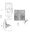
Figure 7a shows how the hole size and spacing can be designed for the resonator ofFigure 5 , andFigure 7b shows the hole pitch desired for different resonator dimensions; and spread of resonant frequencies for a simulated batch of resonators; -
Figure 8 shows in more detail the resonator and suspension design used in the modeling ofFigure 7 ; -
Figure 9 shows four more examples of resonator of the invention which vibration in one dimension; and -
Figure 10a shows simulations for the frequency spread in optimized one-directional bulk-acoustic resonators, andFigure 10b shows simulations for the frequency spread in optimized two-directional bulk-acoustic resonators. - It should be noted that these figures are diagrammatic and not drawn to scale. Relative dimensions and proportions of parts of these figures have been shown exaggerated or reduced in size, for the sake of clarity and convenience in the drawings.
-
Fig. 2 shows a typical square MEMS resonator apparatus according to the prior art to show how the device operates. Theresonator 10 is suspended between a set ofelectrodes 12. In the example pictured, the electrodes are all actuation electrodes applying an input signal Vin to theresonator 10. In this case, the resonator is suspended at its corners. Output measurement is achieved usingconnection contact 14 at one corner, which is electrically connected to the bulk of the resonator. Application of an input signal Vin to theelectrodes 12 exerts electrostatic force on theresonator plate 10. At the same time, the electrodes and plate form a capacitor. Any movement of the plate relative to the electrodes will change the capacitance across the gap. This is precisely what occurs at resonance - the electrostatic forces generated by the AC input signal generate a resonance of the mechanical structure. This results in a capacitance change, which produces an output voltage Vout which is directly related to the time-varying capacitance. - This invention relates to measures for providing tolerance to geometric offset. This has been considered for flex-mode resonators. In these resonators, the resonance frequency of a mechanical resonator depends on its effective stiffness and mass. A mechanical resonator can be modeled by a mass m, spring k and damper system γ. The resonance frequency is given by:

- The key in designs that are insensitive to geometric offset is that the relative change in mass is equal to the relative change in stiffness for an offset.

- This principle can readily be applied to flex-mode resonators.
US 2005/0073078 provides examples of flex-mode designs that are insensitive to geometric offset. - This invention relates specifically to bulk acoustic mode resonators and aims to provide designs which are insensitive to geometric offset for this type of resonator. Bulk-acoustic resonators are much stiffer then flex-mode resonators. Therefore, they can be scaled to much higher frequencies than traditional flex-mode designs. Moreover, the stiffer bulk-acoustic resonator is able to store more energy, which improves phase noise performance.
- For bulk acoustic designs, in order to provide insensitivity to geometric offset. the relative change in wave velocity (v) is equal to the relative change in wavelength (λ).
- The resonance frequency is determined by a longitudinal wave propagating through the material.

- To create a design that is insensitive to geometric offset, the relative dependency of the wave velocity and wavelength on the offset should be made equal.

- In accordance with the invention, this principle is applied to both one-directional and two-directional bulk-acoustic resonators.
- In the fundamental mode, a standing wave of a quarter wavelength (fixed-free) or half wavelength (free-free) propagates in the material. These waves are continuous waves in the material rather than small lattice vibrations. As well as the fundamental mode, the principle also holds for higher order modes.
- Lithography and non-accurate pattern transfer account for the majority of micro-machining variations. Although these variations are temporally random, they are spatially systematic. The inaccuracy can thus be modelled as a systematic geometric offset δ that accounts for the variability in resonator dimensions.
- This geometric offset represents the variation in edge position of the resonator shape edges between different samples created by a given process. This geometric offset is process dependent and is more or less fixed. This means that the offset has a larger effect on smaller structures.
- Variations in dimensions lead to spread in the resonance frequency. In
Figure 3 the systematic offset δ is indicated for a square-plate resonator (without the suspension arrangement shown). The systematic offset δ leads to variation in resonator dimensions. The offset δ is assumed to be constant for the whole structure. For a positive offset, the outside dimensions become slightly larger than intended, as is indicated by Ldesign and Lreal. Holes in the structure will be slightly smaller based on the same (positive) offset. - The main cause of geometric offset is non-accurate pattern transfer. The trenches and holes that need to be etched in the silicon layer (as shown in
Figure 1 ) are patterned in the resist by lithography. When the pattern is transferred to the silicon (Figure 1 b) , under or over etch occurs. For example, wider trenches and holes can be formed as shown inFigure 1b , which mean that the actual silicon structure shaped by these trenches is smaller. The under and over etch affect the holes and trenches that shape the structure. - For example,
Figure 3 also shows asquare hole 20 of intended size (solid line) and size resulting from the offset (dotted line). - For the bulk-acoustic, square-plate resonator, the resonance frequency is determined by the length of the square.

- The velocity of sound is determined by the material constants; Youngs modulus E and density p. The first eigenmode is observed when the square length L equals half of the bulk-acoustic wavelength λ.
- The scaling of the resonance frequency with plate dimensions is indicated in
Figure 4 , which relates to a bulk-acoustic, square-plate resonator with plate length L. The resonance frequency is measured for five square-plate resonators for which plate length L is reduced by afactor 2 in every step. - If the plate-length L is changed by the geometric offset δ, the resonance frequency will spread. A geometric offset of ± 20 nm can easily result in 1000 ppm frequency spread. If the size of the square plate decreases, the total frequency spread increases.
- Holes in the plate affect the velocity of the bulk-acoustic-wave through the material. In the example in
Figure 3 the holes are square shaped. The principle, however, holds for all shapes, so for example circles, triangles, crosses, slits can also be used. The velocity of the wave is reduced by the holes. If the size of the holes increases, the wave velocity is reduced further. For a square-plate with holes the wave velocity has also become dependant on geometric offset and is no longer constant. - Another method to change the resonance frequency is to add external springs. The square-plate resonator is typically suspended at its four corners. These corner suspensions act as springs.
-
Figure 5 shows a square plate resonator with a single T-shaped corner-suspension (although suspensions will be provided at each corner). The main body is provided with an array of square holes. - For the purposes of FEM simulation (the results of which are below) only one-quarter of the structure needs to be simulated. FEM simulations can be used to find designs that are insensitive to geometric offset. For the square-plate with square holes and T-shaped corner suspension in
Figure 5 , such a design has been made at 52 MHz. - This compensated design has been simulated, using three designs that have been given a geometric offset of -100, -50, and +50 nm respectively.
- Measurements on these four designs show that the design has been compensated and that first order frequency dependency on geometrical offset is eliminated. Both measurements and simulations only show a second-order dependency on geometrical offset.
- The results are depicted in
Figure 6 . -
Figure 6a shows the simulated (plot 60 "-") and measured (plot 62 "◆") frequency dependence on the geometric offset δ. - The
plot 62 inFigure 6a shows measured data. An 8 inch wafer containing about 140 identical fields was fabricated. In each field, the 4 resonators were formed. In 80 fields, the 4 resonators were successfully measured and the graph shows the average frequency of these 80 measurements for each of the 4 resonators. - As shown in
Figure 6a , the process variation is expected to be less than 150nm, for a size of resonator of between 50 and 400µm. - In
Figure 6b , a histogram of the compensated design is plotted. For the 80 measured resonators on the wafer more than 90% of the measured resonators are within ± 150 ppm of the average frequency. The dominant source of the measured frequency spread in the histogram is no longer caused by the geometric offset. - The simulation and measurements in
Figure 6 indicate that bulk-acoustic designs can be found that are insensitive to geometric offset. For the square-plate design inFigure 5 , equidistant square holes are used. For a target frequency of 52 MHz it can be shown that for every square hole size an optimized hole pitch can be found. This allows the design to be tailored to the process design rules. - This shows that for a constant hole size, the optimzed pitch depends on the square plate size and thus on the frequency.
- The optimization is carried out by finite-element-simulation (FEM).
- Bulk acoustic designs of a wide frequency range can be compensated for geometrical offset. The results of simulation can be found in
Figure 7 . -
Figures 7a and 7b show the results of FEM simulation on compensated square plate designs as indicated inFigure 5 . All these designs are insensitive to geometric offset. InFigure 7a , the optimal hole pitch is shown for four different square hole sizes (dimension h). This is on a 52 MHz design and for L = 80 µm. InFigure 7b , the optimal hole pitch is shown for resonators of increased size L for hole size 0.5 µm (plot "□") and hole size 1.1 µm (plot "▲"). - There are many combinations of L, h, and pitch that lead to a compensated design.
Figure 7 shows the general relationships between these parameters in compensated designs. - Thus, all the points in
Figure 7a and 7b correspond to compensated designs.Figure 7 thus gives 11 combinations of L,h, and pitch that lead to compensation (the points with dotted lines inFigures 7a and 7b correspond to the same solution). The trends for compensated designs that can be recognized from this figure are: - At constant plate size L (as in
Figure 7a ), a larger pitch requires a larger hole size. - For constant hole size h, a larger plate L requires a larger pitch of the holes.
- One solution is shown in both
Figures 7a and 7b , of a hole size of 0.5 µm, a pitch of 11.5 µm suitable for a resonator length of 80µm. The points inFigures 7a and 7b which correspond to this solution have dotted lines leading to the axes. - The solutions shown in
Figure 7 are based on a resonator design shown in more detail inFigure 8 . There are four "T" shaped anchors connected to the four corners, and the dimensions are shown in the enlarged part of the figure. - The parameters for the solutions shown in
Figure 7a are given in further detail below. In this table, Fres= resonance frequency, L=square plate size, h=hole size, Nh=number of holes in one row/column, pitch=distance between two holes in one row/column, w1, w2, l1, l2 = dimensions of the corner suspension.fres 52.707 52.669 52.665 52.569 L 80 80 80 80 h 0.35 0.5 0.6 1.01 Nh 8 7 6 5 pitch 10.00 11.43 13.33 16.00 w1 2 2 2 2 l1 4 4 4 4 w2 2 2 2 2 l2 20 20 20 20 - The parameters for the solutions shown in
Figure 7b are given in further detail below, showing the same information as the table above.fres 110.391 52.669 23.282 12.82 86.398 52.569 26.9773 12.6408 L 38 80 182 340 49 80 156 335 1/L 0.026316 0.0125 0.005495 0.002941 0.020408 0.0125 0.00641 0.002985 h 0.5 0.5 0.5 0.5 1.01 1.01 1.01 1.01 Nh 5 7 9 13 3 5 7 9 pitch 7.60 11.43 20.22 26.15 16.33 16.00 22.29 37.22 1/pitch 0.13 0.09 0.05 0.04 0.06 0.06 0.04 0.03 w1 1 2 4 8 1 2 4 8 l1 2 4 8 16 2 4 8 16 w2 1 2 4 8 1 2 4 8 l2 10 20 40 80 10 20 40 80 - In the experiments explained above, the square-plate design of
Figure 5 has been used. This design has T-shaped corner suspensions and equidistant square holes. There are however many possible square-plate designs, for example suspended in the middle or on the edge having equidistant, non-equidistant, or even randomly placed holes of all sorts of shapes. It will be clear to those skilled in the art that all these designs can use the same principle to compensate for geometric offset. - The square plate design is a two-directional, bulk-acoustic resonator. The compensation principle also holds for one-directional, bulk-acoustic resonators.
- Thus, for one-directional, bulk-acoustic resonators the same method as for two-directional, bulk-acoustic resonators can be used. The acoustic wavelength is already dependent on geometric offset. By adding holes, the wave velocity again becomes dependent on geometric offset. For a beam with holes an optimized pitch can be found that makes the structure insensitive to geometric offset. Again, this holds for holes of all shapes and sizes. The holes can be placed in an equidistant pattern or randomly over the structure.
- There is also a second approach to create compensated structures. If the structure has a non-uniform cross-section, the acoustic wave will show a phase jump over this boundary. At resonance, the standing wave in the structure is composed of multiple standing waves with different wavelengths. This is most easily explained with reference to a one-directional, bulk-acoustic resonator.
- As an example, a resonator with uniform thickness and only one step change in width is shown in
Figure 9a . This resonator has an effective bulk-acoustic-wavelength that depends on the geometric dimensions of both parts. This is thus a function of four variables that all depend on the geometric offset. Finding the parameters L1, W1, L2, and W2 for which the derivative to the geometric offset of this function is zero can optimize the design. To improve the design further, the second-order derivative can also be made zero.
- This method can also work for two-directional devices, but examples are less straightforward to give. One example could be a square plate design that has a non-uniform layer thickness.
- If a wave hits a physical boundary, part will be transmitted and part will be reflected. For example this is analogous to a wave in a fluid that crosses a boundary in depth, or light hitting a prism. At resonance, the standing wave in the structure is composed of two parts of different wavelength that connect at the boundary. Over this boundary, the composed standing wave shows a discontinuity in phase. An abrupt transition of width can be used, but also a sloped boundary (e.g. a linearly increasing width) can also be considered.
- Essentially, a standing wave is required in each portion. For boundary conditions, the design needs to be robust and needs to be processed with high precision. Thus minimum and maximum widths should be set, for example 200 nm and 200 µs.
- The desired tolerance to process variations can be achieved with two parts to the resonator, although more complicated designs are of course possible.
-
Figure 9 shows three further examples of one-directional, bulk-acoustic resonators that are insensitive to geometric offset. All resonators vibrate in a longitudinal mode. An optimized design can use holes as explained for the square plate resonator. An example of this is the resonator inFigure 9d . However, as explained above, a width variation along the vibration direction of the structure can also make the resonator insensitive to geometric offset. Examples are shown inFigures 9a to 9c . -
Figure 9a shows a design which simply uses a width variation.Figure 9b shows a design which combines a width variation with holes in the wider part and a slot in the narrower part.Figure 9c shows a design which has constant width but uses a slot instead of an array of holes. -
Figure 10 shows FEM simulations for optimized one-directional (Figure 9a ) and two-directional (Figure 9b ) bulk-acoustic resonators. For a geometric offset range of ± 50 nm, frequency spread is reduced to only a few ppm. - Bulk-acoustic resonators are preferred over flex-mode resonators, because of their increased effective stiffness. This is important for:
- (i) Scaling to higher frequencies. Flex-mode resonators are difficult to make for high frequencies (e.g. above 10 MHz), especially thin resonators that vibrate laterally. For these resonators, Q-factors and signal levels decrease significantly at higher frequencies. Bulk-acoustic resonators are a better choice for higher frequencies. Bulk-acoustic resonators have been presented with fundamental frequencies over 1 GHz.
- (ii) Improved phase noise performance. With their high stiffness, bulk-acoustic resonators are able to store more vibration energy than a flex-mode resonator. This improves the signal-to-noise ratio of the resonator.
- (iii) Higher Q-factor. Because of their large energy storage capability (and low anchor losses) bulk-acoustic resonators have very high Q-factors over 105 .
- The MEMS resonators can be processed on 1.5 µm thick SOI wafers. These SOI wafers are available with very constant device layer thickness. By using thin SOI substrates, surface micro machining with standard CMOS processing tools can be used to fabricate the MEMS resonators. With the high accuracy lithography steppers available, geometric offset is reduced to ± 20 nm.
- For typical time-keeping and frequency reference applications a high accuracy is required. For mid-end applications an accuracy of about 100 ppm is required. With a geometric offset of ± 20 nm, the bulk-acoustic resonators will show 1000 ppm frequency spread or more. The invention enables this frequency spread to be recued, for one-directional and two-directional bulk-acoustic resonators to a few ppm for this processing window of ± 20 nm. By providing a design solution, there is no extra cost, since no extra mask layers, process steps, or trimming procedure is needed.
- There are two fundamental approaches outlined above, a first is to use apertures (holes or slots) and the other is to use changes in width or thickness of the resonator body. For one-directional designs, a step change in width is preferred, whereas for the two-directional, square-plate resonator the use of apertures is preferred.
- The detailed examples above use equidistant square holes. However, equidistant round holes can be used, or an irregular pattern of holes, and of any shape.
- It will be apparent from the description above that modeling enables a large number of solutions to be found to provide the desired compensation for geometric offset.
- The invention is of particular interest for the entry of MEMS resonators into the time-keeping and frequency reference market.
- Various other modifications will be apparent to those skilled in the art.
Claims (15)
- A bulk-acoustic-mode MEMS resonator, comprising a resonator body having a first portion with a first physical layout, and a layout modification feature, wherein the resonant frequency is a function of the physical layout of the first portion and the physical layout of the layout modification feature, wherein the physical layouts are designed such that the frequency variation is less than 150ppm for a variation in edge position of the resonator shape edges of 50nm.
- A resonator as claimed in claim 1, wherein the first derivative of frequency with respect to the edge position variation is substantially zero.
- A resonator as claimed in claim 1, wherein the layout modification feature and the first portion have different lateral cross-sections along a principal vibration direction.
- A resonator as claimed in claim 1, wherein the layout modification feature comprises holes or slits within the first portion.
- A resonator as claimed in claim 4, wherein the holes or slits have a dimension smaller than the acoustic wavelength.
- A resonator as claimed in any preceding claim, wherein the resonant vibration is in a one-directional or two-directional mode.
- A resonator as claimed in claim 1, further comprising external suspension springs.
- A resonator as claimed in any preceding claim, wherein the physical layouts are designed such that the frequency variation is less than 100ppm for a variation in edge position of the resonator shape edges of 50nm.
- A resonator as claimed in any preceding claim, wherein the physical layouts are designed such that the frequency variation is less than 150ppm for a variation in edge position of the resonator shape edges of 100nm.
- A resonator as claimed in any preceding claim, further comprising an actuation arrangement, which uses electrostatic actuation or thermal actuation.
- A resonator as claimed in any preceding claim, further comprising a readout arrangement, which uses capacitive readout, piezoresistive readout or piezoelectric readout.
- A method of designing a bulk-acoustic-mode MEMS resonator, comprising;
designing a resonator body having a first portion with a first physical layout, and a layout modification feature;
modeling the resonant frequency, taking into account the physical layout of the first portion and the physical layout of the layout modification feature,
selecting the physical layouts such that the frequency variation is less than a first threshold for a variation in edge position of the resonator shape edges of a second threshold. - A method as claimed in claim 12, wherein the first threshold is 150ppm and the second threshold is 50nm.
- A method as claimed in claim 13, wherein the modeling is carried out using finite element analysis.
- A method as claimed in claim 12, 13 or 14, wherein:the layout modification feature comprises holes or slits within the first portion, and wherein the modeling takes into account the hole or slit dimensions and positions, the first portion dimensions and any suspension system for the resonator body, orthe layout modification feature comprises a portion of different lateral cross-section along a principal vibration direction to the first portion, and wherein the modeling takes into account the lateral cross sections and dimensions of the first portion and the layout modification feature, and any suspension system for the resonator body.
Priority Applications (5)
| Application Number | Priority Date | Filing Date | Title |
|---|---|---|---|
| EP09100232A EP2239845A1 (en) | 2009-04-09 | 2009-04-09 | MEMS resonator |
| US13/263,746 US9800223B2 (en) | 2009-04-09 | 2010-04-07 | MEMS resonator |
| EP10716106A EP2417700A1 (en) | 2009-04-09 | 2010-04-07 | Mems resonator |
| CN201080016032.0A CN102388533B (en) | 2009-04-09 | 2010-04-07 | Mems resonator |
| PCT/IB2010/051505 WO2010116332A1 (en) | 2009-04-09 | 2010-04-07 | Mems resonator |
Applications Claiming Priority (1)
| Application Number | Priority Date | Filing Date | Title |
|---|---|---|---|
| EP09100232A EP2239845A1 (en) | 2009-04-09 | 2009-04-09 | MEMS resonator |
Publications (1)
| Publication Number | Publication Date |
|---|---|
| EP2239845A1 true EP2239845A1 (en) | 2010-10-13 |
Family
ID=41146218
Family Applications (2)
| Application Number | Title | Priority Date | Filing Date |
|---|---|---|---|
| EP09100232A Withdrawn EP2239845A1 (en) | 2009-04-09 | 2009-04-09 | MEMS resonator |
| EP10716106A Withdrawn EP2417700A1 (en) | 2009-04-09 | 2010-04-07 | Mems resonator |
Family Applications After (1)
| Application Number | Title | Priority Date | Filing Date |
|---|---|---|---|
| EP10716106A Withdrawn EP2417700A1 (en) | 2009-04-09 | 2010-04-07 | Mems resonator |
Country Status (4)
| Country | Link |
|---|---|
| US (1) | US9800223B2 (en) |
| EP (2) | EP2239845A1 (en) |
| CN (1) | CN102388533B (en) |
| WO (1) | WO2010116332A1 (en) |
Cited By (2)
| Publication number | Priority date | Publication date | Assignee | Title |
|---|---|---|---|---|
| WO2011061402A1 (en) * | 2009-11-19 | 2011-05-26 | Valtion Teknillinen Tutkimuskeskus | Bulk acoustic wave resonator and method of manufacturing thereof |
| WO2023070214A1 (en) | 2021-10-26 | 2023-05-04 | Stathera Ip Holdings Inc. | Microelectromechanical devices for higher order passive temperature compensation and methods of designing thereof |
Families Citing this family (15)
| Publication number | Priority date | Publication date | Assignee | Title |
|---|---|---|---|---|
| EP2400662B1 (en) | 2010-06-18 | 2015-11-04 | Nxp B.V. | Micro-electromechanical resonator geometry |
| EP2506430B1 (en) | 2011-03-28 | 2017-11-22 | Nxp B.V. | Resonator and method of controlling the same |
| EP2515436A1 (en) | 2011-04-18 | 2012-10-24 | Nxp B.V. | MEMS resonator and method of controlling the same |
| EP2713509B1 (en) | 2012-09-27 | 2015-03-25 | Nxp B.V. | MEMS resonator with improved amplitude saturation |
| DE102012111889B9 (en) | 2012-12-06 | 2014-09-04 | Epcos Ag | Electroacoustic transducer |
| US9208274B2 (en) * | 2013-03-15 | 2015-12-08 | Resonant Inc. | Network synthesis design of microwave acoustic wave filters |
| CN103338022B (en) * | 2013-07-22 | 2016-03-09 | 中国科学院半导体研究所 | The MEMS resonator of frequency-adjustable |
| CN104617360B (en) * | 2013-11-05 | 2018-04-27 | 中国科学院半导体研究所 | The MEMS filter of frequency-adjustable |
| CN103716009B (en) * | 2013-12-23 | 2017-06-23 | 汇隆电子(金华)有限公司 | Mems resonator |
| CN103825493B (en) * | 2014-02-20 | 2016-02-10 | 东南大学 | Perforate hybrid beam vibrational energy self-powered microsensor in Internet of Things radio-frequency receiving-transmitting assembly |
| KR102452948B1 (en) * | 2017-07-18 | 2022-10-11 | 삼성전자주식회사 | micromechanical resonator and resonator system including the same |
| CN109546986B (en) * | 2018-11-29 | 2021-09-03 | 中国科学院半导体研究所 | RF-MEMS resonator support structure for reducing energy loss |
| CN110775936B (en) * | 2019-11-18 | 2023-04-11 | 中国电子科技集团公司第二十六研究所 | Miniature three-dimensional stacked MEMS (micro-electromechanical systems) resonance device |
| CN112398458B (en) * | 2020-11-23 | 2024-10-11 | 浙江铭道通信技术有限公司 | MEMS piezoelectric resonator capable of adjusting frequency based on resonator through hole |
| CN112653408B (en) * | 2020-12-11 | 2022-12-27 | 电子科技大学 | TPoS resonator with real-time fine-tuning working frequency and processing method thereof |
Citations (3)
| Publication number | Priority date | Publication date | Assignee | Title |
|---|---|---|---|---|
| US20050073078A1 (en) | 2003-10-03 | 2005-04-07 | Markus Lutz | Frequency compensated oscillator design for process tolerances |
| US20080143217A1 (en) * | 2006-12-13 | 2008-06-19 | Gavin Kar-Fai Ho | Process compensated micromechanical resonators |
| US20080186109A1 (en) * | 2006-12-13 | 2008-08-07 | Gavin Kar-Fai Ho | Low frequency process-variation-insensitive termperature-stable micromechanical resonators |
Family Cites Families (3)
| Publication number | Priority date | Publication date | Assignee | Title |
|---|---|---|---|---|
| US7749792B2 (en) * | 2004-06-02 | 2010-07-06 | Carnegie Mellon University | Self-assembling MEMS devices having thermal actuation |
| US7642692B1 (en) * | 2005-09-15 | 2010-01-05 | The United States Of America As Represented By The Secretary Of The Army | PZT MEMS resonant Lorentz force magnetometer |
| US7616077B1 (en) * | 2007-03-22 | 2009-11-10 | Sandia Corporation | Microelectromechanical resonator and method for fabrication |
-
2009
- 2009-04-09 EP EP09100232A patent/EP2239845A1/en not_active Withdrawn
-
2010
- 2010-04-07 US US13/263,746 patent/US9800223B2/en active Active
- 2010-04-07 EP EP10716106A patent/EP2417700A1/en not_active Withdrawn
- 2010-04-07 CN CN201080016032.0A patent/CN102388533B/en not_active Expired - Fee Related
- 2010-04-07 WO PCT/IB2010/051505 patent/WO2010116332A1/en not_active Ceased
Patent Citations (3)
| Publication number | Priority date | Publication date | Assignee | Title |
|---|---|---|---|---|
| US20050073078A1 (en) | 2003-10-03 | 2005-04-07 | Markus Lutz | Frequency compensated oscillator design for process tolerances |
| US20080143217A1 (en) * | 2006-12-13 | 2008-06-19 | Gavin Kar-Fai Ho | Process compensated micromechanical resonators |
| US20080186109A1 (en) * | 2006-12-13 | 2008-08-07 | Gavin Kar-Fai Ho | Low frequency process-variation-insensitive termperature-stable micromechanical resonators |
Non-Patent Citations (1)
| Title |
|---|
| GROGG D ET AL: "Bulk lateral MEM resonator on thin SOI with high Q-factor", JOURNAL OF MICROELECTROMECHANICAL SYSTEMS,, vol. 18, no. 2, 1 April 2009 (2009-04-01), pages 466 - 479, XP002701541 * |
Cited By (3)
| Publication number | Priority date | Publication date | Assignee | Title |
|---|---|---|---|---|
| WO2011061402A1 (en) * | 2009-11-19 | 2011-05-26 | Valtion Teknillinen Tutkimuskeskus | Bulk acoustic wave resonator and method of manufacturing thereof |
| WO2023070214A1 (en) | 2021-10-26 | 2023-05-04 | Stathera Ip Holdings Inc. | Microelectromechanical devices for higher order passive temperature compensation and methods of designing thereof |
| EP4423005A4 (en) * | 2021-10-26 | 2025-10-15 | Stathera Ip Holdings Inc | Microelectromechanical devices for passive higher-order temperature compensation and design methods therefor |
Also Published As
| Publication number | Publication date |
|---|---|
| WO2010116332A1 (en) | 2010-10-14 |
| CN102388533B (en) | 2015-09-23 |
| EP2417700A1 (en) | 2012-02-15 |
| US9800223B2 (en) | 2017-10-24 |
| CN102388533A (en) | 2012-03-21 |
| US20120187507A1 (en) | 2012-07-26 |
Similar Documents
| Publication | Publication Date | Title |
|---|---|---|
| EP2239845A1 (en) | MEMS resonator | |
| US11146228B2 (en) | Frequency compensated oscillator design for process tolerances | |
| KR101694133B1 (en) | A micromechanical resonator | |
| US7564162B2 (en) | Process compensated micromechanical resonators | |
| US7616077B1 (en) | Microelectromechanical resonator and method for fabrication | |
| Yantchev et al. | Thin film Lamb wave resonators in frequency control and sensing applications: a review | |
| EP2603976B1 (en) | Micromechanical resonator and method for manufacturing thereof | |
| US7176770B2 (en) | Capacitive vertical silicon bulk acoustic resonator | |
| US9300227B2 (en) | Monolithic body MEMS devices | |
| JP2013511881A (en) | Bulk acoustic wave resonator and manufacturing method thereof | |
| JP5105279B2 (en) | Oscillator and oscillator having the oscillator | |
| US8607630B2 (en) | Vibrating nano-scale or micro-scale electromechanical component with enhanced detection level | |
| Awad et al. | Enhancement of the quality factor of thin-film-piezoelectric-on-Si MEMS resonator using BOX shape phononic crystal | |
| Bengashier | Design and fabrication of RF MEMS devices for wide-band VHF applications | |
| Wu et al. | A High-Q Coupled Dual-Beam Piezoelectric MEMS Resonator for Frequency Control Applications | |
| Zhang | Electrostatic free-free beam microelectromechanical resonator | |
| Harrington | Performance enhancement of micromachined thin-film piezoelectric-on-silicon lateral-extensional resonators through substrate and tether modifications | |
| Samarao et al. | QUALITY FACTOR SE SITIVITY TO CRYSTALLOGRAPHIC AXIS MISALIG ME TI SILICO MICROMECHA ICAL RESO ATORS | |
| Wittwer et al. | Microelectromechanical resonator and method for fabrication | |
| Muriuki et al. | Shunt Tuning of a Piezoelectric Cantilever Beam Resonator | |
| JP2011083844A (en) | Evaluation method for mems device, and manufacturing method for mems device |
Legal Events
| Date | Code | Title | Description |
|---|---|---|---|
| PUAI | Public reference made under article 153(3) epc to a published international application that has entered the european phase |
Free format text: ORIGINAL CODE: 0009012 |
|
| AK | Designated contracting states |
Kind code of ref document: A1 Designated state(s): AT BE BG CH CY CZ DE DK EE ES FI FR GB GR HR HU IE IS IT LI LT LU LV MC MK MT NL NO PL PT RO SE SI SK TR |
|
| 17P | Request for examination filed |
Effective date: 20110413 |
|
| 17Q | First examination report despatched |
Effective date: 20110504 |
|
| STAA | Information on the status of an ep patent application or granted ep patent |
Free format text: STATUS: THE APPLICATION IS DEEMED TO BE WITHDRAWN |
|
| 18D | Application deemed to be withdrawn |
Effective date: 20150825 |