EP2239796A2 - Herstellungsverfahren für ein Widerstandsschaltelement mit Nanolückenelektroden - Google Patents
Herstellungsverfahren für ein Widerstandsschaltelement mit Nanolückenelektroden Download PDFInfo
- Publication number
- EP2239796A2 EP2239796A2 EP20100159482 EP10159482A EP2239796A2 EP 2239796 A2 EP2239796 A2 EP 2239796A2 EP 20100159482 EP20100159482 EP 20100159482 EP 10159482 A EP10159482 A EP 10159482A EP 2239796 A2 EP2239796 A2 EP 2239796A2
- Authority
- EP
- European Patent Office
- Prior art keywords
- electrode
- spacer
- stopper
- forming
- insulating film
- Prior art date
- Legal status (The legal status is an assumption and is not a legal conclusion. Google has not performed a legal analysis and makes no representation as to the accuracy of the status listed.)
- Granted
Links
- 238000004519 manufacturing process Methods 0.000 title claims abstract description 118
- 125000006850 spacer group Chemical group 0.000 claims abstract description 322
- 238000000034 method Methods 0.000 claims abstract description 119
- 230000000994 depressogenic effect Effects 0.000 claims description 147
- VYPSYNLAJGMNEJ-UHFFFAOYSA-N Silicium dioxide Chemical compound O=[Si]=O VYPSYNLAJGMNEJ-UHFFFAOYSA-N 0.000 claims description 20
- 229910052814 silicon oxide Inorganic materials 0.000 claims description 20
- 229910052581 Si3N4 Inorganic materials 0.000 claims description 7
- HQVNEWCFYHHQES-UHFFFAOYSA-N silicon nitride Chemical compound N12[Si]34N5[Si]62N3[Si]51N64 HQVNEWCFYHHQES-UHFFFAOYSA-N 0.000 claims description 7
- 238000012986 modification Methods 0.000 description 60
- 230000004048 modification Effects 0.000 description 60
- 239000000758 substrate Substances 0.000 description 41
- 238000010586 diagram Methods 0.000 description 35
- 239000000463 material Substances 0.000 description 35
- 238000005530 etching Methods 0.000 description 29
- 230000008020 evaporation Effects 0.000 description 8
- 238000001704 evaporation Methods 0.000 description 8
- 238000000623 plasma-assisted chemical vapour deposition Methods 0.000 description 8
- 239000007788 liquid Substances 0.000 description 7
- 229910052751 metal Inorganic materials 0.000 description 6
- 239000002184 metal Substances 0.000 description 6
- 238000007789 sealing Methods 0.000 description 6
- PCHJSUWPFVWCPO-UHFFFAOYSA-N gold Chemical compound [Au] PCHJSUWPFVWCPO-UHFFFAOYSA-N 0.000 description 5
- 229910052737 gold Inorganic materials 0.000 description 5
- 239000010931 gold Substances 0.000 description 5
- VYZAMTAEIAYCRO-UHFFFAOYSA-N Chromium Chemical compound [Cr] VYZAMTAEIAYCRO-UHFFFAOYSA-N 0.000 description 4
- PXHVJJICTQNCMI-UHFFFAOYSA-N Nickel Chemical compound [Ni] PXHVJJICTQNCMI-UHFFFAOYSA-N 0.000 description 4
- KDLHZDBZIXYQEI-UHFFFAOYSA-N Palladium Chemical compound [Pd] KDLHZDBZIXYQEI-UHFFFAOYSA-N 0.000 description 4
- BASFCYQUMIYNBI-UHFFFAOYSA-N platinum Chemical compound [Pt] BASFCYQUMIYNBI-UHFFFAOYSA-N 0.000 description 4
- RYGMFSIKBFXOCR-UHFFFAOYSA-N Copper Chemical compound [Cu] RYGMFSIKBFXOCR-UHFFFAOYSA-N 0.000 description 3
- QPLDLSVMHZLSFG-UHFFFAOYSA-N Copper oxide Chemical compound [Cu]=O QPLDLSVMHZLSFG-UHFFFAOYSA-N 0.000 description 3
- PNEYBMLMFCGWSK-UHFFFAOYSA-N aluminium oxide Inorganic materials [O-2].[O-2].[O-2].[Al+3].[Al+3] PNEYBMLMFCGWSK-UHFFFAOYSA-N 0.000 description 3
- 229910052802 copper Inorganic materials 0.000 description 3
- 239000010949 copper Substances 0.000 description 3
- 238000002715 modification method Methods 0.000 description 3
- OKTJSMMVPCPJKN-UHFFFAOYSA-N Carbon Chemical compound [C] OKTJSMMVPCPJKN-UHFFFAOYSA-N 0.000 description 2
- 239000005751 Copper oxide Substances 0.000 description 2
- BQCADISMDOOEFD-UHFFFAOYSA-N Silver Chemical compound [Ag] BQCADISMDOOEFD-UHFFFAOYSA-N 0.000 description 2
- 229910020776 SixNy Inorganic materials 0.000 description 2
- 229910020781 SixOy Inorganic materials 0.000 description 2
- QAOWNCQODCNURD-UHFFFAOYSA-N Sulfuric acid Chemical compound OS(O)(=O)=O QAOWNCQODCNURD-UHFFFAOYSA-N 0.000 description 2
- 229910045601 alloy Inorganic materials 0.000 description 2
- 239000000956 alloy Substances 0.000 description 2
- 229910052782 aluminium Inorganic materials 0.000 description 2
- XAGFODPZIPBFFR-UHFFFAOYSA-N aluminium Chemical compound [Al] XAGFODPZIPBFFR-UHFFFAOYSA-N 0.000 description 2
- 229910052799 carbon Inorganic materials 0.000 description 2
- 229910017052 cobalt Inorganic materials 0.000 description 2
- 239000010941 cobalt Substances 0.000 description 2
- GUTLYIVDDKVIGB-UHFFFAOYSA-N cobalt atom Chemical compound [Co] GUTLYIVDDKVIGB-UHFFFAOYSA-N 0.000 description 2
- 229910000431 copper oxide Inorganic materials 0.000 description 2
- 229910052593 corundum Inorganic materials 0.000 description 2
- 239000007772 electrode material Substances 0.000 description 2
- 229910052732 germanium Inorganic materials 0.000 description 2
- GNPVGFCGXDBREM-UHFFFAOYSA-N germanium atom Chemical compound [Ge] GNPVGFCGXDBREM-UHFFFAOYSA-N 0.000 description 2
- 239000011521 glass Substances 0.000 description 2
- 229910052759 nickel Inorganic materials 0.000 description 2
- 150000004767 nitrides Chemical class 0.000 description 2
- 229910052763 palladium Inorganic materials 0.000 description 2
- 229910052697 platinum Inorganic materials 0.000 description 2
- 229910052703 rhodium Inorganic materials 0.000 description 2
- 239000010948 rhodium Substances 0.000 description 2
- MHOVAHRLVXNVSD-UHFFFAOYSA-N rhodium atom Chemical compound [Rh] MHOVAHRLVXNVSD-UHFFFAOYSA-N 0.000 description 2
- 229910052709 silver Inorganic materials 0.000 description 2
- 239000004332 silver Substances 0.000 description 2
- 229910052715 tantalum Inorganic materials 0.000 description 2
- GUVRBAGPIYLISA-UHFFFAOYSA-N tantalum atom Chemical compound [Ta] GUVRBAGPIYLISA-UHFFFAOYSA-N 0.000 description 2
- WFKWXMTUELFFGS-UHFFFAOYSA-N tungsten Chemical compound [W] WFKWXMTUELFFGS-UHFFFAOYSA-N 0.000 description 2
- 229910052721 tungsten Inorganic materials 0.000 description 2
- 239000010937 tungsten Substances 0.000 description 2
- 229910001845 yogo sapphire Inorganic materials 0.000 description 2
- BERDEBHAJNAUOM-UHFFFAOYSA-N copper(I) oxide Inorganic materials [Cu]O[Cu] BERDEBHAJNAUOM-UHFFFAOYSA-N 0.000 description 1
- KRFJLUBVMFXRPN-UHFFFAOYSA-N cuprous oxide Chemical compound [O-2].[Cu+].[Cu+] KRFJLUBVMFXRPN-UHFFFAOYSA-N 0.000 description 1
- 238000001312 dry etching Methods 0.000 description 1
- 238000005259 measurement Methods 0.000 description 1
- 230000003647 oxidation Effects 0.000 description 1
- 238000007254 oxidation reaction Methods 0.000 description 1
- 239000004065 semiconductor Substances 0.000 description 1
- 238000001039 wet etching Methods 0.000 description 1
Images










Classifications
-
- H—ELECTRICITY
- H10—SEMICONDUCTOR DEVICES; ELECTRIC SOLID-STATE DEVICES NOT OTHERWISE PROVIDED FOR
- H10N—ELECTRIC SOLID-STATE DEVICES NOT OTHERWISE PROVIDED FOR
- H10N70/00—Solid-state devices having no potential barriers, and specially adapted for rectifying, amplifying, oscillating or switching
- H10N70/801—Constructional details of multistable switching devices
- H10N70/821—Device geometry
- H10N70/826—Device geometry adapted for essentially vertical current flow, e.g. sandwich or pillar type devices
-
- H—ELECTRICITY
- H10—SEMICONDUCTOR DEVICES; ELECTRIC SOLID-STATE DEVICES NOT OTHERWISE PROVIDED FOR
- H10N—ELECTRIC SOLID-STATE DEVICES NOT OTHERWISE PROVIDED FOR
- H10N70/00—Solid-state devices having no potential barriers, and specially adapted for rectifying, amplifying, oscillating or switching
- H10N70/011—Manufacture or treatment of multistable switching devices
-
- H—ELECTRICITY
- H10—SEMICONDUCTOR DEVICES; ELECTRIC SOLID-STATE DEVICES NOT OTHERWISE PROVIDED FOR
- H10N—ELECTRIC SOLID-STATE DEVICES NOT OTHERWISE PROVIDED FOR
- H10N70/00—Solid-state devices having no potential barriers, and specially adapted for rectifying, amplifying, oscillating or switching
- H10N70/20—Multistable switching devices, e.g. memristors
-
- Y—GENERAL TAGGING OF NEW TECHNOLOGICAL DEVELOPMENTS; GENERAL TAGGING OF CROSS-SECTIONAL TECHNOLOGIES SPANNING OVER SEVERAL SECTIONS OF THE IPC; TECHNICAL SUBJECTS COVERED BY FORMER USPC CROSS-REFERENCE ART COLLECTIONS [XRACs] AND DIGESTS
- Y10—TECHNICAL SUBJECTS COVERED BY FORMER USPC
- Y10T—TECHNICAL SUBJECTS COVERED BY FORMER US CLASSIFICATION
- Y10T29/00—Metal working
- Y10T29/49—Method of mechanical manufacture
- Y10T29/49002—Electrical device making
- Y10T29/49082—Resistor making
-
- Y—GENERAL TAGGING OF NEW TECHNOLOGICAL DEVELOPMENTS; GENERAL TAGGING OF CROSS-SECTIONAL TECHNOLOGIES SPANNING OVER SEVERAL SECTIONS OF THE IPC; TECHNICAL SUBJECTS COVERED BY FORMER USPC CROSS-REFERENCE ART COLLECTIONS [XRACs] AND DIGESTS
- Y10—TECHNICAL SUBJECTS COVERED BY FORMER USPC
- Y10T—TECHNICAL SUBJECTS COVERED BY FORMER US CLASSIFICATION
- Y10T29/00—Metal working
- Y10T29/49—Method of mechanical manufacture
- Y10T29/49002—Electrical device making
- Y10T29/49105—Switch making
Definitions
- the present invention relates to a method of fabricating an element including nanogap electrodes.
- an element is developed including silicon oxide and gold which are stable material and the element is fabricated by a simple fabricating method called shadow evaporation.
- the element can be repeatedly used stably in switching operation (for example, Japanese Patent Application Laid-Open Publication No. 2005-79335 ).
- an element which can be integrated at a higher density and which is more easier to integrate is developed, and the element includes two electrodes aligned vertically with a nanogap therebetween (for example, Japanese Patent Application Laid-Open Publication No. 2008-243986 ).
- the element described above is fabricated by the following steps for example, (a) forming a lower electrode (first electrode) on an upper surface of an insulating substrate, (b) forming an insulating film so as to cover the first electrode, (c) forming a depressed section (depressed section on hole) on the insulating film to expose a portion of the upper surface of the first electrode (d) forming an upper electrode (second electrode) in the opening section and inside the depressed section on the upper surface of the insulating film by shadow evaporation and with this, nanogap electrodes are formed.
- the depressed section is fabricated by forming a resist pattern on an insulating film using a device to expose light, etc., and then etching only portions on the insulating film where the resist pattern is not formed. Due to the influence of variation of light exposure and variation of etching, variation of shape of the depressed section occurs. Also, in the element described in Japanese Patent Application Laid-Open Publication No. 2008-243986 , the electrodes are fabricated by shadow evaporation and due to the influence of variation of shadowing angle in shadow evaporation, variation of the shapes of the electrodes occurs. Therefore, there is a problem that it is difficult to perform mass production of elements including nanogap electrodes with a certain distance therebetween due to the influence of variation in fabrication.
- a main object of the present invention to provide a fabrication method of an element including nanogap electrodes, in which an element including nanogap electrodes with a certain distance therebetween can be easily mass produced.
- a fabrication method of an element with nanogap electrodes including a first electrode, a second electrode provided above the first electrode, and a gap provided between the first electrode and the second electrode, the gap being in an order of nanometer to allow resistive state to be switched by applying a predetermined voltage between the first electrode and the second electrode, the method including:
- a fabrication method of an element with nanogap electrodes including a first electrode, a second electrode provided above the first electrode, and a gap provided between the first electrode and the second electrode, the gap being in an order of nanometer to allow resistive state to be switched by applying a predetermined voltage between the first electrode and the second electrode, the method including:
- a fabrication method of an element with nanogap electrodes including a first electrode, a second electrode provided above the first electrode, and a gap provided between the first electrode and the second electrode, the gap being in an order of nanometer to allow resistive state to be switched by applying a predetermined voltage between the first electrode and the second electrode, the method including:
- An element 1 (hereinafter referred to as "nanogap element 1") including nanogap electrodes fabricated by the fabrication method of the present embodiment includes, for example, as shown in the right figure of FIG. 1 , insulating substrate 10, first electrode 20 provided on an upper surface of the insulating substrate 10, insulating film 40 provided on an upper surface of the insulating substrate 10 so as to cover the first electrode 20 with a gap to be separated from the upper surface of the first electrode 20, a depressed section 50 provided on the insulating film 40 to expose a portion of the upper surface of the first electrode 20, a second electrode 60 supported by the insulating film 40 and provided above the first electrode 20 and gap 70 with an order in a unit of nanometers provided between the first electrode 20 and the second electrode 60.
- the first electrode 20 and the second electrode 60 are positioned separated by a fine gap 70 (nanogap) and compose nanogap electrodes.
- the nanogap element 1 (element of right figure of FIG. 1 ) is fabricated by removing a spacer 30 to form a gap 70 from an element (element of left figure of FIG. 1 ) configured including, the insulating substrate 10, the first electrode 20 provided in contact with the upper surface of the insulating substrate 10, spacer 30 provided in contact with the upper surface of the first electrode 20, the insulating film 40 provided so as to be in contact with the upper surface of the insulating substrate 10 and the upper surface of the spacer 30 and to cover the spacer 30 and the first electrode 20 including the spacer 30 on its upper surface, the depressed section 50 provided on the insulating film 40 to expose a portion of the upper surface of the spacer 30, and the second electrode 60 provided so as to be in contact with the upper surface of the insulating film 40, inner face of the depressed section 50 and part of the portion of the upper surface of the spacer 30 exposed by the depressed section 50.
- thickness of the spacer 30 is a size of the gap 70 provided between the two electrodes (first electrode 20 and second electrode 60) of the nanogap element 1.
- the gap 70 with a desired size can be formed without influence of fabrication variation and with high reproducibility.
- the distance between the nanogap electrodes depends on only the thickness of the spacer 30 and does not depend on the shape of the depressed section 50 or the shape of the electrode 20 or 60.
- the size of the gap 70 does not receive the influence of fabrication variation such as variation of light exposure, variation of etching, variation of shadowing angle, etc., and therefore high reproducibility can be achieved and also it is easy to control distance between the nanogap electrodes.
- the thickness (film thickness) of the spacer 30 can be controlled at a level of 0.1 nm, and even when the nanogap element 1 is mass produced (specifically, for example, when the nanogap element 1 is fabricated in orders of billions), the nanogap element 1 with a certain distance between the nanogap electrodes and with a desired distance between the nanogap electrodes can be fabricated.
- the resistive state switches by applying predetermined voltage between the first electrode 20 and the second electrode 60 and the gap 70 is provided with a function to realize a switching phenomenon (switching phenomenon of a resistive state) of the nanogap element 1.
- the thickness of the spacer 30 is not limited and can be any thickness which can form the gap 70 including a size where the resistive state is switched when the predetermined voltage is applied between the first electrode 20 and the second electrode 60.
- the size (G) of the gap 70 can be determined freely to any size where the resistive state is switched when the predetermined voltage is applied between the first electrode 20 and the second electrode 60 and for example, it is preferable that the size is 0 nm ⁇ G ⁇ 13 nm and even more preferable that the size is 0.8 nm ⁇ G ⁇ 2.2 nm.
- the reason why the maximum value of the size G is 13 nm is because when the size G is larger than 13 nm, the resistive state is not switched by applying the predetermined voltage between the first electrode 20 and the second electrode 60.
- the minimum value of the size G is to be larger than 0 nm because when the value is 0 nm, the first electrode 20 and the second electrode 60 is short circuited. Although the minimum value is difficult to determine by measurement with a microscope, the distance can be said to be the minimum distance where a tunnel current occurs. In other words, the minimum value is the theoretical value of the distance where a quantum mechanical tunnel current can be observed without current-voltage characteristics obeying Ohm's law when the nanogap element 1 operates.
- the range of 0.8 nm ⁇ G ⁇ 2.2 nm can be obtained as the calculated result of the size G.
- a predetermined etching gas is a gas which etches the spacer 30, but does not etch sections (insulating substrate 10, first electrode 20, insulating film 40 and second electrode 60) composing the nanogap element 1.
- material of the spacer 30, material of each section composing the nanogap element 1, type of etching gas to remove the spacer 30, etc. is not limited if only the spacer 30 can be selectively removed.
- the insulating substrate 10 includes a function as a support for providing the electrode (first electrode 20) of the nanogap element 1.
- the configuration of the insulating substrate 10 is not limited and for example, the shape of the surface of the insulating substrate 10 can be level or uneven.
- the material of the insulating substrate 10 is not limited if the insulating substrate 10 is not etched when the spacer 30 is removed (etched).
- the insulating substrate 10 can be, for example a semiconductor substrate such as Si provided with an oxide film, etc. on its surface or the insulating substrate 10 can be a substrate in which the substrate itself is insulating.
- the insulating substrate 10 As material of the insulating substrate 10, it is preferable to use glass, oxides such as silicon oxide (SiO 2 ), etc., nitrides such as silicon nitride (Si x N y , Si x O y N z , etc.), or the like and among these, silicon oxide (SiO 2 ) is preferable because adhesion with the first electrode 20 is high and degree of freedom in fabrication is high.
- oxides such as silicon oxide (SiO 2 ), etc.
- nitrides such as silicon nitride (Si x N y , Si x O y N z , etc.)
- silicon oxide (SiO 2 ) is preferable because adhesion with the first electrode 20 is high and degree of freedom in fabrication is high.
- the first electrode 20 is to be a pair with the second electrode 60 and a predetermined voltage is applied so as to allow the nanogap element 1 to perform the switching operation (switching operation of resistive state).
- the shape of the first electrode 20 is not limited and can be suitably modified.
- the material of the first electrode 20 is not limited if the first electrode 20 is not etched when the spacer 30 is removed (etched). Specifically, it is preferable that the material of the first electrode 20 is selected from at least one of, for example, gold, silver, platinum, palladium, nickel, aluminum, cobalt, chrome, rhodium, copper, tungsten, tantalum, carbon, germanium and alloys thereof.
- the first electrode 20 can be a laminated (multi-layer) configuration of chrome and gold.
- the first electrode 20 can be an electrode made from electrode material other than metal.
- the insulating film 40 functions as a support to provide the two electrodes (first electrode 20 and second electrode 60) of the nanogap element 1 apart.
- the configuration of the insulating film 40 is not limited and for example, the shape of the surface of the insulating film 40 can be level or uneven.
- the material of the insulating film 40 is not limited if the insulating film 40 is not etched when the spacer 30 is removed (etched).
- material of the insulating film 40 it is preferable to use glass, oxides such as silicon oxide (SiO 2 ), etc., nitrides such as silicon nitride (Si x N y , Si x O y N z , etc.), or the like and among these, silicon oxide (SiO 2 ) is preferable because adhesion with the first electrode 20 and the second electrode 60 is high and degree of freedom in fabrication is high.
- the insulating film 40 can be formed by overlapping two or more layers of different material.
- the second electrode 60 is to be a pair with the first electrode 20 and a predetermined voltage is applied so as to allow the nanogap element 1 to perform the switching operation (switching operation of resistive state).
- the shape of the second electrode 60 is not limited and can be suitably modified.
- the material of the second electrode 60 is not limited if the second electrode 60 is not etched when the spacer 30 is removed (etched). Specifically, it is preferable that the material of the second electrode 60 is selected from at least one of, for example, gold, silver, platinum, palladium, nickel, aluminum, cobalt, chrome, rhodium, copper, tungsten, tantalum, carbon, germanium and alloys thereof.
- the second electrode 60 can be a laminated (multi-layer) configuration of chrome and gold.
- the second electrode 60 can be an electrode made from electrode material other than metal.
- the fabrication method of the nanogap element 1 for example, the fabrication method of the nanogap element 1 arranged in an array (two dimensional array) as shown in FIG. 3 to FIG. 8 is described as an example.
- FIG. 3 to FIG. 8 shows a fabrication method of a nanogap element 1 arranged in a 2 ⁇ 2 array.
- the nanogap element 1 fabricated by the fabrication method of the present embodiment can be a single one (for example, nanogap element 1 shown in FIG. 1 ) not arranged in an array or arranged in an array other than 2 ⁇ 2.
- the fabrication method of the nanogap element 1 includes, for example, [1] first electrode forming step (step S1), [2] spacer forming step (step S2), [3] insulating film forming step (step S3), [4] depressed section forming step (step S4), [5] second electrode forming step (step S5) and [6] spacer removing step (step S6).
- the first electrode forming step is a step to form the first electrode 20.
- a plurality of first electrodes 20 are formed on the upper surface of the insulating substrate 10 parallel in a line at a predetermined interval.
- a first resist pattern to form the first electrode 20 and the spacer 30 is formed on the upper surface of the insulating substrate 10.
- the first electrode 20 is formed in a portion where the first resist pattern is not formed on the upper surface of the insulating substrate 10 by using a predetermined evaporation device.
- the spacer forming step is a step to form the spacer 30 on the upper surface of the first electrode 20.
- the spacer 30 is formed on substantially the entire upper surface of the first electrode 20 using PECVD (Plasma Enhanced Chemical Vapor Deposition), or the like.
- PECVD Plasma Enhanced Chemical Vapor Deposition
- only the first resist pattern is removed by using a peeling liquid suitable for the material of the first resist pattern.
- the insulating film forming step is a step to form the insulating film 40 to cover the spacer 30 and the first electrode 20 including the spacer 30 on its upper surface.
- the insulating film 40 is formed on substantially the entire upper surface of the insulating substrate 10 using PECVD or the like.
- the depressed section forming step is a step to form the depressed section 50 on the insulating film 40 to expose a portion of the upper surface of the spacer 30.
- a plurality of depressed sections 50 are formed parallel in a line along the line of the first electrode 20.
- a second resist pattern to form the depressed section 50 is formed on the upper surface of the insulating film 40 using, for example, a light exposure device, etc.
- an etching gas suitable for the material of the insulating film 40 is used to selectively remove only the portion where the second resist pattern is not formed on the insulating film 40 to form the depressed section 50.
- the peeling liquid suitable for the material of the second resist pattern is used to remove only the second resist pattern.
- etching gas suitable for the material of the insulating film 40 is not limited if the gas etches the insulating film 40 but does not etch the spacer 30.
- gas such as C 4 F 8 can be preferably used as the etching gas suitable for the material of the insulating film 40.
- the second electrode forming step is a step to form the second electrode 60 in contact with the upper surface of the spacer 30.
- the second electrode 60 is formed so as to be in contact with at least a portion of the spacer 30 exposed by the depressed section 50 and a plurality of second electrodes 60 are formed parallel in a line at a predetermined interval so as to be substantially orthogonal to the line of the first electrodes 20.
- a third resist pattern to form the second electrode 60 is formed on the upper surface of the insulating film 40 and the spacer 30.
- the second electrode 60 is formed in a portion where the third resist pattern is not formed on the upper surface of the insulating film 40 and the upper surface of the spacer 30 by using a predetermined evaporation device.
- the peeling liquid suitable for the material of the third resist pattern is used to remove only the third resist pattern.
- the spacer removing step is a step to form the gap 70 by removing the spacer 30.
- the etching gas suitable for the material of the spacer 30 is used to selectively remove only the spacer 30.
- a nanogap element 1 as shown in FIG. 8 is fabricated.
- the etching gas suitable for the material of the spacer 30 is not limited if the etching gas etches the spacer 30 but does not etch each section (insulating substrate 10, first electrode 20, insulating film 40 and second electrode 60) composing the nanogap element 1.
- the insulating substrate 10 and the insulating film 40 include silicon oxide (SiO 2 ) and the spacer 30 includes silicon nitride (for example SiN), as etching gas suitable for the material of the spacer 30, mixed gas including CF 4 gas, O 2 gas and N 2 gas can be preferably used.
- the insulating substrate 10 and the insulating film 40 include silicon oxide (SiO 2 ) and the spacer 30 includes alumina (Al 2 O 3 ), as etching gas suitable for the material of the spacer 30, gas of the Cl system can be preferably used.
- the fabrication method of the nanogap element 1 as described above is one example and the method is not limited to the above.
- the depressed section 50 is formed on the insulating film 40 so as to expose a portion of the upper surface of the spacer 30.
- the depressed section 50 for example, substantially the entire upper surface of the spacer 30 can be exposed by the depressed section 50.
- the nanogap element 1 can be positioned at a high density when positioned in, for example, an array.
- the spacer 30 is removed by dry etching (in other words, by using an etching gas suitable for the material of the spacer 30).
- the spacer 30 can be removed by wet etching (in other words, by using an etching liquid suitable for the material of the spacer 30).
- step S6 the whole spacer 30 is removed.
- the gap 70 can be formed, removing only a portion of the spacer 30 may be enough.
- a step to form a sealing section (sealing section forming step) to block air from the gap 70 while maintaining the gap 70 can be performed after the spacer removing step (step S6).
- an insulating body can be formed so as to cover the upper surface of the second electrode 60, the upper surface of the insulating film 40 and the opening section of the depressed section 50 to form a sealing section and air can be blocked from the gap 70.
- the sealing section is not limited to a component which covers the opening section of the depressed section 50 and can be any component which can at least block air from the gap 70 while maintaining the gap 70, for example a member which covers the entire nanogap element 1.
- the nanogap element 1 can be used in any desired atmosphere (for example, in the air). Also, the nanogap element 1 (gap 70) can be positioned in a desired atmosphere and by forming a sealing section in this state, the gap 70 can be maintained in a state positioned in the desired atmosphere.
- the fabrication method includes, a first electrode forming step to form the first electrode 20, a spacer forming step to form the spacer 30 on the upper surface of the first electrode 20, a second electrode forming step to form the second electrode 60 in contact with the upper surface of the spacer 30 and a spacer removing step to form the gap 70 by removing the spacer 30.
- the thickness of the spacer 30 is the distance between the nanogap electrodes (size of gap 70 provided between the first electrode 20 and the second electrode 60). Therefore, there is no influence of fabrication variation and the gap 70 with a desired size can be formed with high reproducibility.
- the nanogap element 1 with a certain distance between the nanogap electrodes can be easily mass produced.
- the fabrication method includes an insulating film forming step to form an insulating film 40 to cover the spacer 30 and the first electrode 20 including the spacer 30 on its upper surface, and a depressed section forming step to form the depressed section 50 on the insulating film 40 to expose the upper surface of the spacer 30, and in the second electrode forming step, the second electrode 60 is formed so as to be in contact with the upper surface of the spacer 30 exposed by the depressed section 50.
- the insulating film 40 to support the second electrode 60 is formed (insulating film forming step) and the depressed section 50 is formed on the insulating film 40 (depressed section forming step). Then, the second electrode 60 in contact with the portion of the spacer 30 exposed by the depressed section 50 is formed (second electrode forming step) and the spacer removing step is performed.
- the first electrode 20 is formed parallel in a line with a predetermined interval on the upper surface of the insulating substrate 10
- the depressed section 50 is formed parallel in a line along the first electrode 20 in a line
- the second electrode 60 is formed parallel in a line with a predetermined interval so as to be substantially orthogonal with the first electrode 20 in a line.
- the upper surface of the spacer 30 simultaneously includes a portion in contact with the second electrode 60 and a portion not in contact with the second electrode 60.
- etching gas etching liquid, etc. can also be used
- first the portion of the spacer 30 not in contact with the second electrode 60 is removed and then the portion of the spacer 30 in contact with the second electrode 60 is removed. Since the portion of the spacer 30 in contact with the second electrode 60 is sandwiched by the portions not in contact with the second electrode 60 and the etching gas can easily come into contact, the spacer 30 can be efficiently removed.
- the insulating film 40 includes silicon oxide (SiO 2 ) and the spacer 30 includes silicon nitride (for example, SiN) and in the spacer removing step, the spacer 30 is removed by using mixed gas including CF 4 gas, O 2 gas and N 2 gas.
- step S2 of the above described embodiment PECVD, etc. is used to form the spacer 30 on the first electrode 20.
- the spacer 30 can be formed on the upper surface of the first electrode 20, for example, the spacer 30 can be formed by performing a predetermined surface processing on the upper surface of the first electrode 20.
- the predetermined surface processing is not limited as long as the portion of the first electrode 20 on which the surface processing is not performed is not removed, and only the portion (spacer 30) on which the surface processing is performed can be selectively removed.
- the first electrode 20 includes copper
- the upper surface becomes copper oxide (CuO or Cu 2 O) and the copper oxide is to be the spacer 30.
- dilute sulfuric acid can be preferably used as the etching liquid suitable for the material of the spacer 30.
- the spacer 30 is formed on substantially the entire upper surface of the first electrode 20.
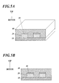
- the spacer 30 is formed on the upper surface of the first electrode 20, for example, as shown in FIG. 9A , the spacer 30 can be formed on a portion of the upper surface of the first electrode 20.
- a nanogap element 1 as shown in FIG. 9B is formed with a portion (portion where the spacer 30 is not formed) of the upper surface of the first electrode 20 in contact with the insulating film 40.
- the spacer 30 is formed on only the upper surface of the first electrode 20.
- the spacer 30 can be formed so as to cover the first electrode 20.
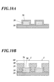
- the spacer 30 needs to support the insulating film 40 in order to maintain a state where the gap 70 is formed. Therefore, for example, as shown in FIG. 10B , a nanogap element 1 is fabricated with the spacer 30 remaining at least between the side face of the first electrode 20 and the insulating film 40 and between the insulating substrate 10 and the insulating film 40.
- the fabrication method of the nanogap element 1 is not limited to the above described embodiment and for example, as shown in FIG. 11 , the fabrication method can include [1] first electrode layer forming step (step S11), [2] spacer layer forming step (step S12), [3] first electrode and spacer forming step (step S13), [4] insulating film forming step (step S3), [5] depressed section forming step (step S4), [6] second electrode forming step (step S5), and [7] spacer removing step (step S6).
- the first electrode layer forming step is a step to form a first electrode layer 20A which is to be a first electrode 20.
- the first electrode layer 20A is formed on substantially the entire upper surface of the insulating substrate 10 by using a predetermined evaporation device.
- the spacer layer forming step is a step to form the spacer layer 30A, which is to be the spacer 30, on the upper surface of the first electrode layer 20A.
- the spacer layer 30A is formed on substantially the entire upper surface of the first electrode layer 20A by using PECVD, etc.
- the spacer layer forming step (step S12) is not limited to forming the spacer layer 30A on the first electrode layer 20A using PECVD, etc., and the spacer layer 30A can be formed by performing predetermined surface processing on the upper surface of the first electrode layer 20A.
- the first electrode and spacer forming step is a step to form the spacer 30 and the first electrode 20 included on the upper surface of the spacer 30 from the first electrode layer 20A and the spacer layer 30A.
- a resist pattern to form the first electrode 20 and the spacer 30 is formed on the upper surface of the spacer layer 30A by using a light exposure device, etc.
- the etching gas suitable for the material of the spacer layer 30A and the spacer 30 is formed.
- the peeling liquid suitable for the material of the resist pattern is used to remove only the resist pattern.
- the insulating film forming step is a step to form an insulating film 40 on substantially the entire upper surface of the insulating substrate 10 to cover the spacer 30 and the first electrode 20 including the spacer 30 on its upper surface.
- the depressed section forming step is a step to form the depressed section 50 on the insulating film 40 to expose a portion of the upper surface of the spacer 30.
- the second electrode forming step is a step to form the second electrode 60 in contact with the upper surface of the spacer 30.
- the spacer removing step is a step to form the gap 70 by removing the spacer 30.
- the nanogap element 1 as shown in FIG. 12D is fabricated.
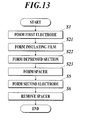
- the modification method can include [1] first electrode forming step (step S1), [2] insulating film forming step (step S21), [3] depressed section forming step (step S22), [4] spacer forming step (step S23), [5] second electrode forming step (step S5), and [6] spacer removing step (step S6).
- the first electrode forming step is a step to form the first electrode 20 on the upper surface of the insulating substrate 10.
- the insulating film forming step is a step to form the insulating film 40 to cover the first electrode 20 on substantially the entire upper surface of the insulating substrate 10.
- the depressed section forming step is a step to form the depressed section 50 on the insulating film 40 to expose a portion of the upper surface of the first electrode 20.
- the depressed section forming step (step S22) is not limited to forming the depressed section 50 on the insulating film 40 to expose a portion of the upper surface of the first electrode 20 and the depressed section 50 can be formed on the insulating film 40 to expose substantially the entire upper surface of the first electrode 20.
- the spacer forming step is a step to form the spacer 30 on the upper surface of the first electrode 20 exposed by the depressed section 50.
- the spacer forming step (step S23) is not limited to forming the spacer 30 on the first electrode 20 using the PECVD, etc., and the spacer 30 can be formed by performing predetermined surface processing on the upper surface of the first electrode 20.
- the second electrode forming step is a step to form the second electrode 60 in contact with the upper surface of the spacer 30.
- the spacer removing step is a step to form the gap 70 by removing the spacer 30.
- a nanogap element 1 as shown in FIG. 14D is fabricated.
- the modification method of the nanogap element 1 is not limited to the above described embodiment and for example, as shown in FIG. 15 , the modification method can include [1] first electrode forming step (step S1), [2] spacer forming step (step S2), [3] stopper forming step (step S31), [4] insulating film forming step (step S32), [5] first depressed section forming step (step S33), [6] second depressed section forming step (step S34), [7] second electrode forming step (step S35), and [8] spacer removing step (step S6).
- the first electrode forming step is a step to form the first electrode 20 on the upper surface of the insulating substrate 10.
- the spacer forming step is a step to form the spacer 30 on the upper surface of the first electrode 20.
- the stopper forming step is a step to form a stopper 80 on the upper surface of the spacer 30.
- the stopper 80 can be formed on substantially the entire upper surface of the spacer 30 or the stopper 80 can be formed on a portion of the upper surface of the spacer 30.
- the insulating film forming step is a step to form an insulating film 40 on substantially the entire upper surface of the insulating substrate 10 to cover the stopper 80, the spacer 30 including the stopper 80 on its upper surface and the first electrode 20 including the spacer 30 on its upper surface.
- the first depressed section forming step is a step to form the first depressed section 50A on the insulating film 40 to expose a portion of the upper surface of the stopper 80.
- the first depressed section forming step (step S33) is not limited to forming the first depressed section 50A on the insulating film 40 to expose a portion of the upper surface of the stopper 80 and the first depressed section 50A can be formed on the insulating film 40 to expose substantially the entire upper surface of the stopper 80.
- the second depressed section forming step is a step to form the second depressed section 50B on the stopper 80 to expose a portion of the upper surface of the spacer 30.
- the second depressed section forming step (step S34) is not limited to forming the second depressed section 50B on the stopper 80 to expose a portion of the upper surface of the spacer 30 and the second depressed section 50B can be formed on the stopper 80 to expose substantially the entire upper surface of the spacer 30.
- the first depressed section 50A is formed using the etching gas suitable for the material of the insulating film 40
- the second depressed section 50B is formed using the etching gas suitable for the material of the stopper 80.
- the etching gas suitable for the material of the insulating film 40 is not limited if the gas etches the insulating film 40 but does not etch the stopper 80. Also, the etching gas suitable for the material of the stopper 80 is not limited if the gas etches the stopper 80 but does not etch the spacer 30. Specifically, for example, when the insulating film 40 includes SiO 2 , the stopper 80 includes Al 2 O 3 , and the spacer 30 includes SiN, C 4 F 8 gas can be preferably used as the etching gas suitable for the material of the insulating film 40 and Cl 2 gas can be preferably used as the etching gas suitable for the material of the stopper 80.
- the second electrode forming step is a step to form the second electrode 60 so as to be in contact with the upper surface of the spacer 30 exposed by the second depressed section 50B.
- the spacer removing step is a step to form the gap 70 by removing the spacer 30.
- the nanogap element 1 shown in FIG. 16E is fabricated.
- the stopper 80 is formed on substantially the entire upper surface of the spacer 30.
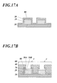
- the stopper 80 can be formed on a portion of the upper surface of the spacer 30 or, for example, as shown in FIG. 17A , the stopper 80 can be formed so as to cover the spacer 30 and the first electrode 20 including the spacer 30 on its upper surface.
- the nanogap element 1 as shown in FIG. 17B is fabricated.
- the spacer 30 is formed on substantially the entire upper surface of the first electrode 20.
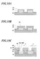
- the spacer 30 can be formed on a portion of the upper surface of the first electrode 20 or, for example, as shown in FIG. 18A , the spacer 30 can be formed so as to cover the first electrode 20.
- the stopper 80 can be formed so as to cover the spacer 30.
- the nanogap element 1 as shown in FIG. 18C is fabricated.
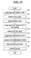
- the fabrication method of the nanogap element 1 is not limited to the above described embodiment and for example, as shown in FIG. 19 , the fabrication method can include the following steps of [1] first electrode layer forming step (step S11), [2] spacer layer forming step (step S12), [3] stopper layer forming step (step S41), [4] first electrode, spacer and stopper forming step (step S42), [5] insulating film forming step (step S32), [6] first depressed section forming step (step S33), [7] second depressed section forming step (step S34), [8] second electrode forming step (step S35), and [9] spacer removing step (step S6).
- the first electrode layer forming step is a step to form the first electrode layer 20A, which is to be the first electrode 20, on substantially the entire upper surface of the insulating substrate 10.
- the spacer layer forming step is a step to form a spacer layer 30A, which is to be the spacer 30, on the upper surface of the first electrode layer 20A.
- the stopper layer forming step is a step to form the stopper layer 80A, which is to be the stopper 80, on the upper surface of the spacer layer 30A.
- the first electrode, spacer and stopper forming step is a step to form the stopper 80, the spacer 30 including the stopper 80 on its upper surface and the first electrode 20 including the spacer 30 on its upper surface from the first electrode layer 20A, spacer layer 30A and stopper layer 80A.
- the insulating film forming step is a step to form the insulating film 40 on substantially the entire upper surface of the insulating substrate 10 to cover the stopper 80, the spacer 30 including the stopper 80 on its upper surface and the first electrode 20 including the spacer 30 on its upper surface.
- the first depressed section forming step is a step to form the first depressed section 50A on the insulating film 40 to expose a portion of the upper surface of the stopper 80.
- the second depressed section forming step is a step to form the second depressed section 50B on the stopper 80 to expose a portion of the upper surface of the spacer 30.
- the second electrode forming step is a step to form the second electrode 60 so as to be in contact with the upper surface of the spacer 30 exposed by the second depressed section 50B.
- the spacer removing step is a step to form the gap 70 by removing the spacer 30.
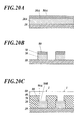
- the nanogap element 1 as shown in FIG. 20C is fabricated.
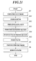
- the fabrication method of the nanogap element 1 is not limited to the above described embodiment, and for example, as shown in FIG. 21 , the fabrication method can include the following steps of, [1] first electrode forming step (step S1), [2] stopper forming step (step S51), [3] insulating film forming step (step S52), [4] first depressed section forming step (step S53), [5] second depressed section forming step (step S54), [6] spacer forming step (step S55), [7] second electrode forming step (step S5), and [8] spacer removing step (step S6).
- the first electrode forming step is a step to form the first electrode 20 on the upper surface of the insulating substrate 10.
- the stopper forming step is a step to form the stopper 80 on the upper surface of the first electrode 20.
- the insulating film forming step is a step to form the insulating film 40 on substantially the entire upper surface of the insulating substrate 10 to cover the stopper 80 and the first electrode 20 including the stopper 80 on its upper surface.
- the first depressed section forming step is a step to form the first depressed section 50A on the insulating film 40 to expose a portion of the upper surface of the stopper 80.
- the first depressed section forming step is not limited to forming the first depressed section 50A on the insulating film 40 to expose a portion of the upper surface of the stopper 80 and the first depressed section 50A can be formed on the insulating film 40 to expose substantially the entire upper surface of the stopper 80.
- the second depressed section forming step is a step to form the second depressed section 50B on the stopper 80 to expose a portion of the upper surface of the first electrode 20.
- the second depressed section forming step (step S54) is not limited to forming the second depressed section 50B on the stopper 80 to expose a portion of the upper surface of the first electrode 20 and the second depressed section 50B can be formed on the stopper 80 to expose substantially the entire upper surface of the first electrode 20.
- the spacer forming step is a step to form the spacer 30 on the upper surface of the first electrode 20 exposed by the second depressed section 50B.
- the second electrode forming step is a step to form the second electrode 60 in contact with the upper surface of the spacer 30.
- the spacer removing step is a step to form the gap 70 by removing the spacer 30.
- the nanogap element 1 as shown in FIG. 22E is fabricated.
- the stopper 80 is formed on substantially the entire upper surface of the first electrode 20.
- the stopper 80 can be formed on a portion of the upper surface of the first electrode 20 and for example, as shown in FIG. 23A , the stopper 80 can be formed so as to cover the first electrode 20.
- the stopper 80 is formed so as to cover the fist electrode 20, for example, the nanogap element 1 as shown in FIG. 23B is fabricated.
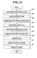
- the fabrication method of the nanogap element 1 is not limited to the above described embodiment, for example, as shown in FIG. 24 , the fabrication method can include the following steps of, [1] first electrode layer forming step (step S11), [2] stopper layer forming step (step S61), [3] first electrode and stopper forming step (step S62), [4] insulating film forming step (step S52), [5] first depressed section forming step (step S53), [6] second depressed section forming step (step S54), [7] spacer forming step (step S55), [8] second electrode forming step (step S5), and [9] spacer removing step (step S6).
- the first electrode layer forming step is a step to form the first electrode layer 20A, which is to be the first electrode 20, on substantially the entire upper surface of the insulating substrate 10.
- the stopper layer forming step is a step to form the stopper layer 80A, which is to be the stopper 80, on the upper surface of the first electrode layer 20A.
- the first electrode and stopper forming step is a step to form the stopper 80 and the first electrode 20 including the stopper 80 on its upper surface from the first electrode layer 20A and the stopper layer 80A.
- the insulating film forming step is a step to form the insulating film 40 on substantially the entire upper surface of the insulating substrate 10 to cover the stopper 80 and the first electrode 20 including the stopper 80 on its upper surface.
- the first depressed section forming step is a step to form the first depressed section 50A on the insulating film 40 to expose a portion of the upper surface of the stopper 80.
- the second depressed section forming step is a step to form the second depressed section 50B on the stopper 80 to expose a portion of the upper surface of the first electrode 20.
- the spacer forming step is a step to form the spacer 30 on the upper surface of the first electrode 20 exposed by the second depressed section 50B.
- the second electrode forming step is a step to form the second electrode 60 in contact with the upper surface of the spacer 30.
- the spacer removing step is a step to form the gap 70 to remove the spacer 30.
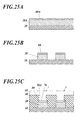
- the nanogap element 1 as shown in FIG. 25C is fabricated.
- the stopper 80 is formed, the insulating film 40 and the stopper 80 are removed separately and the depressed section to expose the upper surface of the spacer 30 is gradually formed. Consequently, compared to when the stopper 80 is not formed, the damage to the spacer 30 is reduced. Therefore, the gap 70 with a desired size can be formed even better without influence of fabrication variation and higher reproducibility.
- the stopper 80 is formed, the insulating film 40 and the stopper 80 are removed separately and the depressed section to expose the upper surface of the first electrode 20 is gradually formed. Consequently, compared to when the stopper 80 is not formed, the damage to the first electrode 20 can be reduced. Therefore, the gap 70 with a desired size can be formed even better without influence of fabrication variation and higher reproducibility.
- the depressed section 50 (in other words, groove section) is formed in a line.
- the shape of the depressed section 50 is not limited to this shape and for example, can be a hole shape.
- a fabrication method of an element with nanogap electrodes including a first electrode, a second electrode provided above the first electrode, and a gap provided between the first electrode and the second electrode, the gap being in an order of nanometer to allow resistive state to be switched by applying a predetermined voltage between the first electrode and the second electrode, the method including:
- a fabrication method of an element with nanogap electrodes including a first electrode, a second electrode provided above the first electrode, and a gap provided between the first electrode and the second electrode, the gap being in an order of nanometer to allow resistive state to be switched by applying a predetermined voltage between the first electrode and the second electrode, the method including:
- the fabrication method of an element with nanogap electrodes further includes:
- the fabrication method of an element with nanogap electrodes further includes:
- the fabrication method of an element with nanogap electrodes further includes:
- the fabrication method of an element with nanogap electrodes further includes:
- the fabrication method of an element with nanogap electrodes further includes:
- a fabrication method of an element with nanogap electrodes including a first electrode, a second electrode provided above the first electrode, and a gap provided between the first electrode and the second electrode, the gap being in an order of nanometer to allow resistive state to be switched by applying a predetermined voltage between the first electrode and the second electrode, the method including:
- the spacer is formed by performing a predetermined surface processing on the upper surface of the first electrode.
- the spacer layer is formed by performing a predetermined surface processing on the upper surface of the first electrode layer.
- the insulating film includes silicon oxide; the spacer includes silicon nitride; and the spacer is removed using mixed gas including CF 4 gas, O 2 gas and N 2 gas.
- the thickness of the spacer is to be the distance between the nanogap electrodes (size of the gap provided between the first and the second electrode) and therefore, the gap with the desired size can be formed without influence of fabrication variation and with high reproducibility.
- the element with a certain distance between the nanogap electrodes can be easily mass produced.
Landscapes
- Engineering & Computer Science (AREA)
- Manufacturing & Machinery (AREA)
- Semiconductor Memories (AREA)
- Bipolar Transistors (AREA)
- Junction Field-Effect Transistors (AREA)
Applications Claiming Priority (1)
| Application Number | Priority Date | Filing Date | Title |
|---|---|---|---|
| JP2009095575A JP5455415B2 (ja) | 2009-04-10 | 2009-04-10 | ナノギャップ電極を有する素子の製造方法 |
Publications (3)
| Publication Number | Publication Date |
|---|---|
| EP2239796A2 true EP2239796A2 (de) | 2010-10-13 |
| EP2239796A3 EP2239796A3 (de) | 2013-05-22 |
| EP2239796B1 EP2239796B1 (de) | 2016-02-17 |
Family
ID=42288700
Family Applications (1)
| Application Number | Title | Priority Date | Filing Date |
|---|---|---|---|
| EP10159482.8A Not-in-force EP2239796B1 (de) | 2009-04-10 | 2010-04-09 | Herstellungsverfahren für ein Widerstandsschaltelement mit Nanolücken-Metallelektroden |
Country Status (3)
| Country | Link |
|---|---|
| US (1) | US9130159B2 (de) |
| EP (1) | EP2239796B1 (de) |
| JP (1) | JP5455415B2 (de) |
Families Citing this family (2)
| Publication number | Priority date | Publication date | Assignee | Title |
|---|---|---|---|---|
| US8470713B2 (en) * | 2010-12-13 | 2013-06-25 | International Business Machines Corporation | Nitride etch for improved spacer uniformity |
| WO2012121067A1 (ja) * | 2011-03-08 | 2012-09-13 | 独立行政法人科学技術振興機構 | ナノギャップ長を有する電極構造の作製方法並びにそれにより得られるナノギャップ長を有する電極構造及びナノデバイス |
Citations (2)
| Publication number | Priority date | Publication date | Assignee | Title |
|---|---|---|---|---|
| JP2005079335A (ja) | 2003-08-29 | 2005-03-24 | National Institute Of Advanced Industrial & Technology | ナノギャップ電極の製造方法及び該方法により製造されたナノギャップ電極を有する素子 |
| JP2008243986A (ja) | 2007-03-26 | 2008-10-09 | Funai Electric Advanced Applied Technology Research Institute Inc | スイッチング素子 |
Family Cites Families (6)
| Publication number | Priority date | Publication date | Assignee | Title |
|---|---|---|---|---|
| US4816098A (en) * | 1987-07-16 | 1989-03-28 | Texas Instruments Incorporated | Apparatus for transferring workpieces |
| JP3647317B2 (ja) * | 1999-06-04 | 2005-05-11 | キヤノン株式会社 | 液体吐出ヘッド用基板、液体吐出ヘッド、前記液体吐出ヘッド用基板の製造方法、及び前記液体吐出ヘッドの製造方法 |
| CN100448049C (zh) * | 2001-09-25 | 2008-12-31 | 独立行政法人科学技术振兴机构 | 使用固体电解质的电气元件和存储装置及其制造方法 |
| US7098577B2 (en) * | 2002-10-21 | 2006-08-29 | Hrl Laboratories, Llc | Piezoelectric switch for tunable electronic components |
| DE10256486A1 (de) * | 2002-12-03 | 2004-07-15 | Infineon Technologies Ag | Verfahren zum Herstellen einer Speicherzelle, Speicherzelle und Speicherzellen-Anordnung |
| JP2009049287A (ja) | 2007-08-22 | 2009-03-05 | Funai Electric Advanced Applied Technology Research Institute Inc | スイッチング素子、スイッチング素子の製造方法及びメモリ素子アレイ |
-
2009
- 2009-04-10 JP JP2009095575A patent/JP5455415B2/ja not_active Expired - Fee Related
-
2010
- 2010-04-08 US US12/756,522 patent/US9130159B2/en not_active Expired - Fee Related
- 2010-04-09 EP EP10159482.8A patent/EP2239796B1/de not_active Not-in-force
Patent Citations (2)
| Publication number | Priority date | Publication date | Assignee | Title |
|---|---|---|---|---|
| JP2005079335A (ja) | 2003-08-29 | 2005-03-24 | National Institute Of Advanced Industrial & Technology | ナノギャップ電極の製造方法及び該方法により製造されたナノギャップ電極を有する素子 |
| JP2008243986A (ja) | 2007-03-26 | 2008-10-09 | Funai Electric Advanced Applied Technology Research Institute Inc | スイッチング素子 |
Also Published As
| Publication number | Publication date |
|---|---|
| US20100257726A1 (en) | 2010-10-14 |
| JP5455415B2 (ja) | 2014-03-26 |
| EP2239796A3 (de) | 2013-05-22 |
| US9130159B2 (en) | 2015-09-08 |
| EP2239796B1 (de) | 2016-02-17 |
| JP2010245471A (ja) | 2010-10-28 |
Similar Documents
| Publication | Publication Date | Title |
|---|---|---|
| US7728320B2 (en) | Semiconductor memory device and phase change memory device | |
| US8043950B2 (en) | Semiconductor device and manufacturing method thereof | |
| US7446044B2 (en) | Carbon nanotube switches for memory, RF communications and sensing applications, and methods of making the same | |
| US10483460B2 (en) | Method of manufacturing a magnetoresistive stack/ structure using plurality of encapsulation layers | |
| US8053730B2 (en) | Infrared sensor and method of fabricating the same | |
| JP2005105416A (ja) | チタンベース材料の選択的等方性エッチングプロセス | |
| US20130020183A1 (en) | Silicide Micromechanical Device and Methods to Fabricate Same | |
| US20020168810A1 (en) | Lateral nanostructures by vertical processing | |
| EP2239796A2 (de) | Herstellungsverfahren für ein Widerstandsschaltelement mit Nanolückenelektroden | |
| WO2005004203A2 (en) | System and method based on field-effect transistors for addressing nanometer-scale devices | |
| US11493471B2 (en) | Sensor | |
| JP2017067446A (ja) | ナノギャップ電極の製造方法、側壁スペーサ、及び側壁スペーサの製造方法 | |
| US7344908B2 (en) | Atomic force microscope cantilever including field effect transistor and method for manufacturing the same | |
| US20170103947A1 (en) | Faceted structure formed by self-limiting etch | |
| KR102559405B1 (ko) | 수소 센서 및 이의 제조 방법 | |
| JP2009123818A (ja) | 磁気センサデバイスの製造方法 | |
| JP5665161B2 (ja) | 圧電薄膜デバイス | |
| CN111108591B (zh) | 形成用于生物应用的自支撑膜的方法 | |
| JP6281383B2 (ja) | 半導体素子 | |
| US12340276B2 (en) | Device for controlling trapped ions with low heat dissipation | |
| KR101694549B1 (ko) | 나노 갭 패턴 형성 방법, 나노 갭 패턴을 갖는 바이오 센서 및 바이오 센서 제조 방법 | |
| EP1325884A2 (de) | MEMS-Struktur, ein starres Opferschichtstütze/Anker enthaltend, und Verfahren zu deren Herstellung | |
| US20040121619A1 (en) | Multipoint minute electrode, device for measuring a living organism voltage, method for fabricating the multipoint minute electrode, and method for fabricating the living organism voltage-measuring device | |
| KR20140026962A (ko) | 그래핀을 이용한 캔틸레버 소자 및 그 제조방법 | |
| US7989904B2 (en) | Micro-electromechanical device and manufacturing method thereof |
Legal Events
| Date | Code | Title | Description |
|---|---|---|---|
| PUAI | Public reference made under article 153(3) epc to a published international application that has entered the european phase |
Free format text: ORIGINAL CODE: 0009012 |
|
| AK | Designated contracting states |
Kind code of ref document: A2 Designated state(s): AT BE BG CH CY CZ DE DK EE ES FI FR GB GR HR HU IE IS IT LI LT LU LV MC MK MT NL NO PL PT RO SE SI SK SM TR |
|
| AX | Request for extension of the european patent |
Extension state: AL BA ME RS |
|
| PUAL | Search report despatched |
Free format text: ORIGINAL CODE: 0009013 |
|
| AK | Designated contracting states |
Kind code of ref document: A3 Designated state(s): AT BE BG CH CY CZ DE DK EE ES FI FR GB GR HR HU IE IS IT LI LT LU LV MC MK MT NL NO PL PT RO SE SI SK SM TR |
|
| AX | Request for extension of the european patent |
Extension state: AL BA ME RS |
|
| RIC1 | Information provided on ipc code assigned before grant |
Ipc: H01L 45/00 20060101AFI20130412BHEP |
|
| 17P | Request for examination filed |
Effective date: 20130902 |
|
| RBV | Designated contracting states (corrected) |
Designated state(s): AT BE BG CH CY CZ DE DK EE ES FI FR GB GR HR HU IE IS IT LI LT LU LV MC MK MT NL NO PL PT RO SE SI SK SM TR |
|
| 17Q | First examination report despatched |
Effective date: 20140228 |
|
| RAP1 | Party data changed (applicant data changed or rights of an application transferred) |
Owner name: FUNAI ELECTRIC CO., LTD. |
|
| GRAP | Despatch of communication of intention to grant a patent |
Free format text: ORIGINAL CODE: EPIDOSNIGR1 |
|
| INTG | Intention to grant announced |
Effective date: 20150805 |
|
| GRAS | Grant fee paid |
Free format text: ORIGINAL CODE: EPIDOSNIGR3 |
|
| GRAA | (expected) grant |
Free format text: ORIGINAL CODE: 0009210 |
|
| AK | Designated contracting states |
Kind code of ref document: B1 Designated state(s): AT BE BG CH CY CZ DE DK EE ES FI FR GB GR HR HU IE IS IT LI LT LU LV MC MK MT NL NO PL PT RO SE SI SK SM TR |
|
| REG | Reference to a national code |
Ref country code: GB Ref legal event code: FG4D |
|
| REG | Reference to a national code |
Ref country code: CH Ref legal event code: EP |
|
| REG | Reference to a national code |
Ref country code: IE Ref legal event code: FG4D |
|
| REG | Reference to a national code |
Ref country code: AT Ref legal event code: REF Ref document number: 775998 Country of ref document: AT Kind code of ref document: T Effective date: 20160315 |
|
| REG | Reference to a national code |
Ref country code: DE Ref legal event code: R096 Ref document number: 602010030638 Country of ref document: DE |
|
| REG | Reference to a national code |
Ref country code: NL Ref legal event code: MP Effective date: 20160217 |
|
| REG | Reference to a national code |
Ref country code: LT Ref legal event code: MG4D |
|
| REG | Reference to a national code |
Ref country code: AT Ref legal event code: MK05 Ref document number: 775998 Country of ref document: AT Kind code of ref document: T Effective date: 20160217 |
|
| PG25 | Lapsed in a contracting state [announced via postgrant information from national office to epo] |
Ref country code: ES Free format text: LAPSE BECAUSE OF FAILURE TO SUBMIT A TRANSLATION OF THE DESCRIPTION OR TO PAY THE FEE WITHIN THE PRESCRIBED TIME-LIMIT Effective date: 20160217 Ref country code: NO Free format text: LAPSE BECAUSE OF FAILURE TO SUBMIT A TRANSLATION OF THE DESCRIPTION OR TO PAY THE FEE WITHIN THE PRESCRIBED TIME-LIMIT Effective date: 20160517 Ref country code: IT Free format text: LAPSE BECAUSE OF FAILURE TO SUBMIT A TRANSLATION OF THE DESCRIPTION OR TO PAY THE FEE WITHIN THE PRESCRIBED TIME-LIMIT Effective date: 20160217 Ref country code: GR Free format text: LAPSE BECAUSE OF FAILURE TO SUBMIT A TRANSLATION OF THE DESCRIPTION OR TO PAY THE FEE WITHIN THE PRESCRIBED TIME-LIMIT Effective date: 20160518 Ref country code: FI Free format text: LAPSE BECAUSE OF FAILURE TO SUBMIT A TRANSLATION OF THE DESCRIPTION OR TO PAY THE FEE WITHIN THE PRESCRIBED TIME-LIMIT Effective date: 20160217 |
|
| PG25 | Lapsed in a contracting state [announced via postgrant information from national office to epo] |
Ref country code: PL Free format text: LAPSE BECAUSE OF FAILURE TO SUBMIT A TRANSLATION OF THE DESCRIPTION OR TO PAY THE FEE WITHIN THE PRESCRIBED TIME-LIMIT Effective date: 20160217 Ref country code: BE Free format text: LAPSE BECAUSE OF NON-PAYMENT OF DUE FEES Effective date: 20160430 Ref country code: AT Free format text: LAPSE BECAUSE OF FAILURE TO SUBMIT A TRANSLATION OF THE DESCRIPTION OR TO PAY THE FEE WITHIN THE PRESCRIBED TIME-LIMIT Effective date: 20160217 Ref country code: LT Free format text: LAPSE BECAUSE OF FAILURE TO SUBMIT A TRANSLATION OF THE DESCRIPTION OR TO PAY THE FEE WITHIN THE PRESCRIBED TIME-LIMIT Effective date: 20160217 Ref country code: PT Free format text: LAPSE BECAUSE OF FAILURE TO SUBMIT A TRANSLATION OF THE DESCRIPTION OR TO PAY THE FEE WITHIN THE PRESCRIBED TIME-LIMIT Effective date: 20160617 Ref country code: SE Free format text: LAPSE BECAUSE OF FAILURE TO SUBMIT A TRANSLATION OF THE DESCRIPTION OR TO PAY THE FEE WITHIN THE PRESCRIBED TIME-LIMIT Effective date: 20160217 Ref country code: NL Free format text: LAPSE BECAUSE OF FAILURE TO SUBMIT A TRANSLATION OF THE DESCRIPTION OR TO PAY THE FEE WITHIN THE PRESCRIBED TIME-LIMIT Effective date: 20160217 Ref country code: LV Free format text: LAPSE BECAUSE OF FAILURE TO SUBMIT A TRANSLATION OF THE DESCRIPTION OR TO PAY THE FEE WITHIN THE PRESCRIBED TIME-LIMIT Effective date: 20160217 |
|
| PG25 | Lapsed in a contracting state [announced via postgrant information from national office to epo] |
Ref country code: DK Free format text: LAPSE BECAUSE OF FAILURE TO SUBMIT A TRANSLATION OF THE DESCRIPTION OR TO PAY THE FEE WITHIN THE PRESCRIBED TIME-LIMIT Effective date: 20160217 Ref country code: EE Free format text: LAPSE BECAUSE OF FAILURE TO SUBMIT A TRANSLATION OF THE DESCRIPTION OR TO PAY THE FEE WITHIN THE PRESCRIBED TIME-LIMIT Effective date: 20160217 |
|
| REG | Reference to a national code |
Ref country code: DE Ref legal event code: R097 Ref document number: 602010030638 Country of ref document: DE |
|
| PG25 | Lapsed in a contracting state [announced via postgrant information from national office to epo] |
Ref country code: CZ Free format text: LAPSE BECAUSE OF FAILURE TO SUBMIT A TRANSLATION OF THE DESCRIPTION OR TO PAY THE FEE WITHIN THE PRESCRIBED TIME-LIMIT Effective date: 20160217 Ref country code: SM Free format text: LAPSE BECAUSE OF FAILURE TO SUBMIT A TRANSLATION OF THE DESCRIPTION OR TO PAY THE FEE WITHIN THE PRESCRIBED TIME-LIMIT Effective date: 20160217 Ref country code: RO Free format text: LAPSE BECAUSE OF FAILURE TO SUBMIT A TRANSLATION OF THE DESCRIPTION OR TO PAY THE FEE WITHIN THE PRESCRIBED TIME-LIMIT Effective date: 20160217 Ref country code: SK Free format text: LAPSE BECAUSE OF FAILURE TO SUBMIT A TRANSLATION OF THE DESCRIPTION OR TO PAY THE FEE WITHIN THE PRESCRIBED TIME-LIMIT Effective date: 20160217 |
|
| REG | Reference to a national code |
Ref country code: CH Ref legal event code: PL |
|
| PLBE | No opposition filed within time limit |
Free format text: ORIGINAL CODE: 0009261 |
|
| STAA | Information on the status of an ep patent application or granted ep patent |
Free format text: STATUS: NO OPPOSITION FILED WITHIN TIME LIMIT |
|
| PG25 | Lapsed in a contracting state [announced via postgrant information from national office to epo] |
Ref country code: BE Free format text: LAPSE BECAUSE OF FAILURE TO SUBMIT A TRANSLATION OF THE DESCRIPTION OR TO PAY THE FEE WITHIN THE PRESCRIBED TIME-LIMIT Effective date: 20160217 Ref country code: LU Free format text: LAPSE BECAUSE OF FAILURE TO SUBMIT A TRANSLATION OF THE DESCRIPTION OR TO PAY THE FEE WITHIN THE PRESCRIBED TIME-LIMIT Effective date: 20160409 |
|
| 26N | No opposition filed |
Effective date: 20161118 |
|
| GBPC | Gb: european patent ceased through non-payment of renewal fee |
Effective date: 20160517 |
|
| REG | Reference to a national code |
Ref country code: IE Ref legal event code: MM4A |
|
| REG | Reference to a national code |
Ref country code: FR Ref legal event code: ST Effective date: 20161230 |
|
| PG25 | Lapsed in a contracting state [announced via postgrant information from national office to epo] |
Ref country code: CH Free format text: LAPSE BECAUSE OF NON-PAYMENT OF DUE FEES Effective date: 20160430 Ref country code: LI Free format text: LAPSE BECAUSE OF NON-PAYMENT OF DUE FEES Effective date: 20160430 Ref country code: FR Free format text: LAPSE BECAUSE OF NON-PAYMENT OF DUE FEES Effective date: 20160502 |
|
| PG25 | Lapsed in a contracting state [announced via postgrant information from national office to epo] |
Ref country code: SI Free format text: LAPSE BECAUSE OF FAILURE TO SUBMIT A TRANSLATION OF THE DESCRIPTION OR TO PAY THE FEE WITHIN THE PRESCRIBED TIME-LIMIT Effective date: 20160217 Ref country code: BG Free format text: LAPSE BECAUSE OF FAILURE TO SUBMIT A TRANSLATION OF THE DESCRIPTION OR TO PAY THE FEE WITHIN THE PRESCRIBED TIME-LIMIT Effective date: 20160517 |
|
| PG25 | Lapsed in a contracting state [announced via postgrant information from national office to epo] |
Ref country code: GB Free format text: LAPSE BECAUSE OF NON-PAYMENT OF DUE FEES Effective date: 20160517 Ref country code: IE Free format text: LAPSE BECAUSE OF NON-PAYMENT OF DUE FEES Effective date: 20160409 |
|
| REG | Reference to a national code |
Ref country code: DE Ref legal event code: R084 Ref document number: 602010030638 Country of ref document: DE |
|
| PG25 | Lapsed in a contracting state [announced via postgrant information from national office to epo] |
Ref country code: HU Free format text: LAPSE BECAUSE OF FAILURE TO SUBMIT A TRANSLATION OF THE DESCRIPTION OR TO PAY THE FEE WITHIN THE PRESCRIBED TIME-LIMIT; INVALID AB INITIO Effective date: 20100409 Ref country code: CY Free format text: LAPSE BECAUSE OF FAILURE TO SUBMIT A TRANSLATION OF THE DESCRIPTION OR TO PAY THE FEE WITHIN THE PRESCRIBED TIME-LIMIT Effective date: 20160217 |
|
| PG25 | Lapsed in a contracting state [announced via postgrant information from national office to epo] |
Ref country code: TR Free format text: LAPSE BECAUSE OF FAILURE TO SUBMIT A TRANSLATION OF THE DESCRIPTION OR TO PAY THE FEE WITHIN THE PRESCRIBED TIME-LIMIT Effective date: 20160217 Ref country code: MK Free format text: LAPSE BECAUSE OF FAILURE TO SUBMIT A TRANSLATION OF THE DESCRIPTION OR TO PAY THE FEE WITHIN THE PRESCRIBED TIME-LIMIT Effective date: 20160217 Ref country code: IS Free format text: LAPSE BECAUSE OF FAILURE TO SUBMIT A TRANSLATION OF THE DESCRIPTION OR TO PAY THE FEE WITHIN THE PRESCRIBED TIME-LIMIT Effective date: 20160217 Ref country code: MT Free format text: LAPSE BECAUSE OF NON-PAYMENT OF DUE FEES Effective date: 20160430 Ref country code: HR Free format text: LAPSE BECAUSE OF FAILURE TO SUBMIT A TRANSLATION OF THE DESCRIPTION OR TO PAY THE FEE WITHIN THE PRESCRIBED TIME-LIMIT Effective date: 20160217 Ref country code: MC Free format text: LAPSE BECAUSE OF FAILURE TO SUBMIT A TRANSLATION OF THE DESCRIPTION OR TO PAY THE FEE WITHIN THE PRESCRIBED TIME-LIMIT Effective date: 20160217 |
|
| PGFP | Annual fee paid to national office [announced via postgrant information from national office to epo] |
Ref country code: DE Payment date: 20220302 Year of fee payment: 13 |
|
| REG | Reference to a national code |
Ref country code: DE Ref legal event code: R079 Ref document number: 602010030638 Country of ref document: DE Free format text: PREVIOUS MAIN CLASS: H01L0045000000 Ipc: H10N0070000000 |
|
| REG | Reference to a national code |
Ref country code: DE Ref legal event code: R119 Ref document number: 602010030638 Country of ref document: DE |
|
| PG25 | Lapsed in a contracting state [announced via postgrant information from national office to epo] |
Ref country code: DE Free format text: LAPSE BECAUSE OF NON-PAYMENT OF DUE FEES Effective date: 20231103 |