EP2239591A1 - Current monitor for sensing the current in a current path and corresponding control device - Google Patents
Current monitor for sensing the current in a current path and corresponding control device Download PDFInfo
- Publication number
- EP2239591A1 EP2239591A1 EP09157667A EP09157667A EP2239591A1 EP 2239591 A1 EP2239591 A1 EP 2239591A1 EP 09157667 A EP09157667 A EP 09157667A EP 09157667 A EP09157667 A EP 09157667A EP 2239591 A1 EP2239591 A1 EP 2239591A1
- Authority
- EP
- European Patent Office
- Prior art keywords
- current
- semiconductor device
- monitor
- resistive
- branch
- Prior art date
- Legal status (The legal status is an assumption and is not a legal conclusion. Google has not performed a legal analysis and makes no representation as to the accuracy of the status listed.)
- Granted
Links
Images



Classifications
-
- G—PHYSICS
- G01—MEASURING; TESTING
- G01R—MEASURING ELECTRIC VARIABLES; MEASURING MAGNETIC VARIABLES
- G01R19/00—Arrangements for measuring currents or voltages or for indicating presence or sign thereof
- G01R19/0092—Measuring current only
-
- H—ELECTRICITY
- H03—ELECTRONIC CIRCUITRY
- H03F—AMPLIFIERS
- H03F3/00—Amplifiers with only discharge tubes or only semiconductor devices as amplifying elements
- H03F3/34—DC amplifiers in which all stages are DC-coupled
- H03F3/343—DC amplifiers in which all stages are DC-coupled with semiconductor devices only
- H03F3/3432—DC amplifiers in which all stages are DC-coupled with semiconductor devices only with bipolar transistors
-
- G—PHYSICS
- G01—MEASURING; TESTING
- G01R—MEASURING ELECTRIC VARIABLES; MEASURING MAGNETIC VARIABLES
- G01R1/00—Details of instruments or arrangements of the types included in groups G01R5/00 - G01R13/00 and G01R31/00
- G01R1/20—Modifications of basic electric elements for use in electric measuring instruments; Structural combinations of such elements with such instruments
- G01R1/203—Resistors used for electric measuring, e.g. decade resistors standards, resistors for comparators, series resistors, shunts
-
- G—PHYSICS
- G01—MEASURING; TESTING
- G01R—MEASURING ELECTRIC VARIABLES; MEASURING MAGNETIC VARIABLES
- G01R1/00—Details of instruments or arrangements of the types included in groups G01R5/00 - G01R13/00 and G01R31/00
- G01R1/30—Structural combination of electric measuring instruments with basic electronic circuits, e.g. with amplifier
-
- H—ELECTRICITY
- H03—ELECTRONIC CIRCUITRY
- H03F—AMPLIFIERS
- H03F2200/00—Indexing scheme relating to amplifiers
- H03F2200/462—Indexing scheme relating to amplifiers the current being sensed
Definitions
- the invention relates to a current monitor for sensing the current in a current path, said current monitor comprising a resistive sensing element in a section of said current path and a current mirror circuit comprising a first semiconductor device and a second semiconductor device, both semiconductor devices electrically interconnected with each other for copying the current in the second semiconductor device to the first semiconductor device, wherein the first semiconductor device is electrically connected to an electric reference potential and to a current input side of the section via a resistive equivalence element in a first current branch and wherein the second semiconductor device is electrically connected to the electric reference potential and to a current output side of the section in a second current branch.
- a current monitor comprising a current mirror circuit for measuring the current in the path.
- the current monitor is for example based on a simple current mirror consisting of a pair of transistors electrically interconnected with each other for copying the current of the second transistor to the first transistor.
- the output voltage signal proportional to the current can be measured for example at the resistive equivalence element in the first current branch.
- this signal strongly depends on the potential difference between the potential of the current measuring point in the current path and the reference potential (ground potential GND).
- the simple current mirror shows a broad frequency bandwidth range.
- a current monitor based on a Wilson current mirror with two contrariwise connected pairs of transistors on the contrary provides an output signal widely independent from said potential difference, but the current monitor based on the Wilson current mirror circuit shows low frequency bandwidth range for measuring a current with AC- and DC-portion.
- One application for current monitors for measuring currents with AC- and DC-portion is the use in a control device for controlling a switching stage of a modulator system. For this application a precise measurement of the AC- and DC-portion of a current in a current path with high potential difference to ground potential in a wide frequency bandwidth range is needed.
- US 6,661,217 B2 describes a wideband precision current monitor employing DC-coupled and AC-coupled sensing circuits to generate lower and higher frequency sense signals, which are combined to form a wideband output signal that is proportional to a wideband current of interest.
- the frequency response of the wideband output signal is substantially flat across a wideband frequency range based on matching the frequency response of the DC- and AC-coupled sensing circuits.
- the current monitor according to the invention comprises a constant current source for keeping the current in the second current branch independent from the potential difference between the potential of the current output side of the section and the reference potential.
- the current in the second current branch is copied to the first current branch by the current mirror. Because the current in the second current branch is a potential difference independent current, an output voltage signal measurable at a resistive element -like for example the resistive reference element- in the first current branch is as well independent from the potential difference between the potential of the current output side of the section and the reference potential (and of course independent from the potential difference between the potential of the current input side of the section and the reference potential as well).
- the current mirror circuit of the current monitor can be realized as a simple current mirror or a Wilson current mirror.
- the current mirror circuit is a simple current mirror consisting of just one pair of semiconductor devices electrically interconnected with each providing a wider frequency bandwidth.
- the frequency bandwidth of this simple current monitor is mainly determinate by the transition frequency of its semiconductor devices.
- a resistive output element for measuring its voltage drop is electrically arranged in the first current branch between the first semiconductor device and the reference potential. Because the resistive output element and the resistive equivalence element are connected in series in the first current branch (which is an "unbranched" current path), the ratio Vout/Veq of the voltage drop at the resistive output element Vout and the voltage drop at the resistive equivalence element Veq is given by the ratio of their resistivity Rout/Req. This ratio is an amplification factor of the measurable output voltage signal of the current monitor dropping at the resistive output element compared to the voltage dropping at the resistive reference element.
- a further resistive element is electrically arranged in the second current branch between the second semiconductor device and the reference potential to bring both semiconductor devices (first and second semiconductor device) on a common potential level.
- the constant current source is electrically arranged in the second current branch between the second semiconductor device and the reference potential.
- a constant current source based on the reference potential can be supplied by a voltage supply based on the reference potential.
- the constant current source preferably is electrically arranged in the second current branch between the further resistive element and the reference potential.
- the constant current source comprises a current mirror assembly supplied by a voltage supply.
- a constant current source comprising a current mirror assembly is a simple but effective current source for this application.
- the constant current source further comprises the voltage supply.
- the current monitor further comprises a shunt reference element between the current path and the constant current source for providing the voltage supply of the constant current source.
- the constant current source further comprises a semiconductor component to constitute a diode assembly for compensation of temperature-dependent measurement errors of the current monitor.
- a semiconductor unit is electrically arranged in the first current branch between the first semiconductor device and the resistive output element, wherein said semiconductor unit is controlled by a current of the constant current source.
- the current monitor further comprises a parallel connection circuit of a first diode device and a second diode device being connected parallel to the section of the current path, wherein the two diode devices are anti-parallel connected with respect to each other.
- the first diode device and the second diode device are adapted for limiting the magnitude of the electric signal.
- the first and second semiconductor devices are bipolar transistors or field effect transistors, especially matching each other.
- the bipolar transistors are preferably PNP transistors with a typical transition frequency of about 150 MHz, especially BC856A PNP silicon transistors or BF550 PNP silicon transistors.
- the current mirror circuit is a current mirror circuit with a predetermined bandwidth of ⁇ 20 MHz, preferably of ⁇ 50 MHz, more preferably of ⁇ 100 MHz for measuring the high frequency AC-components of the current in the current path.
- the current mirror circuit is a current mirror circuit adapted for a maximum potential difference between the electrical potential of the input side of the section and the electrical reference potential ⁇ 30 Volts, preferably ⁇ 40 Volts, more preferably ⁇ 50 Volts.
- the current monitor is a current monitor adapted for a maximum electrical current through the resistive sensing element > 5 A, preferably ⁇ 6.6 A.
- the current monitor further comprises a voltage tap electrically connected to the first current path between the first active semiconductor device and the resistive output element to tap an output voltage signal caused by the voltage drop at the resistive output element (Vout).
- the invention further relates to a control device for controlling a switching stage in dependence of a current in a current path, said control device comprising an aforementioned current monitor, further comprising a comparator for converting an analog voltage signal caused by the voltage drop at the resistive output element to a digital switching signal.
- the control device preferably is a control device for controlling the switching stage of a modulator or power management system in dependence of the current in a current path between a power generator and a load.
- Fig. 1 shows a simulation of a typical sensing situation with a current monitor 10 for sensing the current in a current path 12.
- the current path 12 guides from an external ideal current source 14 to an external ideal voltage source 16.
- the ideal current source 14 comprises a DC current source component 18 and an AC current source component 20.
- the voltage source 16 defines a potential difference between the current path 10 and the ground potential (mass) as a reference potential.
- a resistor 22 in the current path 12 defines the resistivity of said path 12.
- the current monitor 10 comprises a resistive sensing element 24 in a section 26 of said current path 12 and a current mirror circuit 28 comprising a first semiconductor device 30 and a second semiconductor device 32.
- the first semiconductor device 30 is electrically integrated in a first current branch 34; the second semiconductor device 32 is electrically integrated in a second current branch 36.
- Both semiconductor devices 30, 32 are electrically interconnected with each other for copying the current in the second semiconductor device 32 (and the second current branch 36 respectively) to the first semiconductor device 30 and the first current branch 34.
- the two semiconductor devices 30, 32 are PNP transistors (BC856 transistors).
- the emitter of the first semiconductor device 30 is electrically connected in a first node to a current input side of the section 26 of the current path 12 via a resistive equivalence element 38 and the collector of the first semiconductor device 30 is electrically connected to ground potential as an electric reference potential.
- the first current branch 34 comprises the first semiconductor device 30, a resistive equivalence element 38 and a resistive output element 40.
- the resistivity value of the resistive equivalence element 38 is equal to resistivity value of the resistive sensing element 24 (1 ⁇ ) to bring or keep the emitters of both semiconductor devices 30, 32 formed as PNP transistors on a common potential level.
- the ratio Vout/Veq of the voltage drop Vout at the resistive output element 40 and the voltage drop Vref at the resistive equivalence element 38 is given by the ratio of their resistivity Rout/Req.
- This ratio is an amplification factor of the measurable output voltage of the current monitor 10.
- the emitter of the second semiconductor device 32 is electrically connected in a second node to a current output side of the section 26 and the collector of the second semiconductor device 32 is electrically connected to the electric reference potential (ground potential).
- a further resistive element 42 is electrically arranged in the second current branch 36 between the second semiconductor device 32 and the reference potential to keep both semiconductor devices (first and second semiconductor device) 30, 32 on a common potential level.
- the second current branch 36 comprises the second semiconductor device 32 and the further resistive element 42.
- the collector and the basis of the second semiconductor device 32 are shorted and the basis of the first and the basis of the second semiconductor device 30, 32 are electrically connected with each other by a line to copy the current in the second semiconductor device 32 (and the second current branch 36 respectively) to the first semiconductor device 30.
- the resistivity of the further resistive element is 1 k ⁇ .
- the current mirror circuit 28 further comprises a constant current source 44 for keeping the current in the second current path 32 independent from the potential difference between the potential of the current output side of the section 26, especially at the second node, and the reference potential (ground potential).
- This constant current source 44 is electrically arranged in the second current branch 36 between the further resistive element 42 and the reference potential.
- the constant current source 44 comprises a (5V-)voltage supply 46 electrically connected in line with a resistor 48 (resistivity: 2 k ⁇ ) on a primary side and a current mirror assembly 50 which comprises a first and second transistor 52, 54 (NPN transistors BC846).
- a resistor 48 resistivity: 2 k ⁇
- a current mirror assembly 50 which comprises a first and second transistor 52, 54 (NPN transistors BC846).
- NPN transistors BC846 NPN transistors BC846
- the output side resistor 56 (resistivity: 300 ⁇ ) is electrically arranged between the second transistor 54 of the current mirror assembly 50 and the reference potential.
- the constant current source 44 further comprises a semiconductor component (NPN transistor BC846) constituting a diode assembly 58 for compensation of temperature-dependent measurement errors of the current monitor 10.
- the diode assembly 58 is electrically connected between the collector of the first transistor 52 and the reference potential.
- the constant current source 44 further comprises a semiconductor unit 60, which is electrically arranged in the first current branch 34 between the first semiconductor device 30 and the resistive output element 40.
- the semiconductor unit 60 is a PNP medium frequency transistor (PNP transistor BF550) being part of a cascade connection of the constant current source 44.
- the current monitor 10 further comprises a parallel connection circuit 62 of a first diode device 64 and a second diode device 66 being connected parallel to the section 26 of the current path 12, wherein the two diode devices 64, 66 are anti-parallel connected with respect to each other.
- the parallel connection circuit 62 with the diode devices 64, 66 limits the maximum voltage drop over the resistive sensing element 24.
- the current monitor 10 further comprises a voltage tap 68 electrically connected to the first current path between the semiconductor unit 60 and the resistive output element 40 to tap an output voltage signal (Vout) caused by the voltage drop at the resistive output element 40.
- Vout output voltage signal
- the current monitor further comprises a shunt reference arrangement for voltage supply of the constant current source 44 (not shown).
- An output voltage signal proportional to the current in the sensing element drops at the resistive output element with respect to the reference potential.
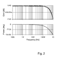
- Fig. 2 shows a simulated output signal gain (upper diagram) and output signal phase (lower diagram) over a frequency range from 100 kHz to 1.0 GHz of the current monitor shown in Fig. 1 .
- the frequency response of the output signal characterizes the behavior of the current monitor 10.
- the cut-off frequency, also referred to as 3 dB cut-off frequency in the following, of the current monitor 10 corresponds to 200 MHz.
- the diagram in Fig. 3 shows the output voltage signal Vout versus the "input voltage", which is the potential difference between the potential of the current input side of the section and the reference potential (ground potential).
- Vout 570 mV.
- Fig. 4 shows a simulated output voltage signal Vout level over a temperature range from 0°C to 100°C varying over this range less than 1 % (from 372.5 V to 375.1 V). This temperature-independent behavior is due to the ideal current source 26 comprising the current mirror assembly 50 and the diode assembly 32.
- Fig. 5 shows the current monitor 10 measuring the current in a current path 12 connecting a current source 14 with a load 72, which is electrically connected to a second current source 74 via an inductive element for simulation reasons.
- Fig. 6 shows a simulated output signal gain (upper diagram) and output signal phase (lower diagram) over a frequency range from 100 kHz to 1.0 GHz at an electric current of 200 mA and a load resistance of 100 ⁇ , as depicted in Fig. 5 .
- the bandwidth of the current monitor 10 corresponds to a value of 10.5 MHz.
- the pre-voltage at an output of the current monitor 10 corresponds to a value of 20 V.
- the frequency response depends on the load 72. The smaller the value of the load 72, the higher the value of the cut-off frequency and thus the larger the bandwidth of the current monitor 10.
- the signal increases at higher frequencies.
- the current monitor 10 is adapted for processing current peaks up to 5 amperes.
- the first diode device 64 and the second diode device 66 are arranged in parallel to the sensing element 24 and operate as a low pass filter as well.
- the capacitance of the diode devices 64, 66 should preferably be selected smaller than 1.6 nF. Since the measurement of the electric current is performed only in the positive flowing direction (from current input side to current output side, also a combination of a silicon diode device and a Schottky diode device is applicable.
- a Schottky diode device shows a small capacitance in the backward direction and a normal silicon diode device, also referred to as PN diode, shows a larger threshold value in the forward direction. It is noted, that the current monitor operates linearly up to 0.5 A.
- Table 1 shows corresponding DC currents and bandwidth ranges of the current monitor 10 for different values of the resistivity of the load 72 simulated in the circuit of Fig. 5 .
- Table 1 Load resistivity, DC current and bandwidth ranges of the current monitor 10 shown in Fig. 5.
- Resistivity of the load 72 DC current in the current path 12 3dB-bandwidth of the current monitor 10 100 Ohms 200mA 10.5 MHz 50 Ohms 400mA 21.0 MHz 20 Ohms 1.0 A 44.4 MHz 10 Ohms 2.0 A 83.7 MHz 5 Ohms 4.0 A 195 MHz 2 Ohms 6.6 A 555 MHz
- a major application for the current monitor 10 adapted for measuring currents with AC- and DC-portion is the use in a control device for controlling a switching stage of a modulator system, especially an envelope tracking modulator, in dependence of the current in a current path between a power generator and a load (not shown).
Landscapes
- Engineering & Computer Science (AREA)
- Power Engineering (AREA)
- Physics & Mathematics (AREA)
- General Physics & Mathematics (AREA)
- Measurement Of Current Or Voltage (AREA)
- Control Of Electrical Variables (AREA)
Abstract
Description
- The invention relates to a current monitor for sensing the current in a current path, said current monitor comprising a resistive sensing element in a section of said current path and a current mirror circuit comprising a first semiconductor device and a second semiconductor device, both semiconductor devices electrically interconnected with each other for copying the current in the second semiconductor device to the first semiconductor device, wherein the first semiconductor device is electrically connected to an electric reference potential and to a current input side of the section via a resistive equivalence element in a first current branch and wherein the second semiconductor device is electrically connected to the electric reference potential and to a current output side of the section in a second current branch.
- A current monitor comprising a current mirror circuit for measuring the current in the path is known. The current monitor is for example based on a simple current mirror consisting of a pair of transistors electrically interconnected with each other for copying the current of the second transistor to the first transistor. The output voltage signal proportional to the current can be measured for example at the resistive equivalence element in the first current branch. In a current monitor based on the simple current mirror this signal strongly depends on the potential difference between the potential of the current measuring point in the current path and the reference potential (ground potential GND). On the other hand the simple current mirror shows a broad frequency bandwidth range.
- A current monitor based on a Wilson current mirror with two contrariwise connected pairs of transistors on the contrary provides an output signal widely independent from said potential difference, but the current monitor based on the Wilson current mirror circuit shows low frequency bandwidth range for measuring a current with AC- and DC-portion.
- One application for current monitors for measuring currents with AC- and DC-portion is the use in a control device for controlling a switching stage of a modulator system. For this application a precise measurement of the AC- and DC-portion of a current in a current path with high potential difference to ground potential in a wide frequency bandwidth range is needed.
-
US 6,661,217 B2 describes a wideband precision current monitor employing DC-coupled and AC-coupled sensing circuits to generate lower and higher frequency sense signals, which are combined to form a wideband output signal that is proportional to a wideband current of interest. The frequency response of the wideband output signal is substantially flat across a wideband frequency range based on matching the frequency response of the DC- and AC-coupled sensing circuits. - It is the object of the invention to provide a simple and low priced current monitor with an enhanced frequency bandwidth range for measuring a current consisting of an AC- and DC-portion with an output voltage signal independent from a potential difference between the potential of the current measuring point in the current path and the reference potential.
- This object is achieved by the present invention as defined in claim 1. The current monitor according to the invention comprises a constant current source for keeping the current in the second current branch independent from the potential difference between the potential of the current output side of the section and the reference potential. The current in the second current branch is copied to the first current branch by the current mirror. Because the current in the second current branch is a potential difference independent current, an output voltage signal measurable at a resistive element -like for example the resistive reference element- in the first current branch is as well independent from the potential difference between the potential of the current output side of the section and the reference potential (and of course independent from the potential difference between the potential of the current input side of the section and the reference potential as well).
- The resistivity of the resistive equivalence element is chosen in such way, that the first and second semiconductor devices are on a common electrical potential. In the absence of other resistive elements -except for the resistive sensing element- in the section of the current path and/or the section of the second current branch between the current output side and the second semiconductor device, the resistivity of the resistive equivalence element is equal to the resistivity of the resistive sensing element (Rsens = Req).
- In general the current mirror circuit of the current monitor can be realized as a simple current mirror or a Wilson current mirror. Preferably, the current mirror circuit is a simple current mirror consisting of just one pair of semiconductor devices electrically interconnected with each providing a wider frequency bandwidth. The frequency bandwidth of this simple current monitor is mainly determinate by the transition frequency of its semiconductor devices.
- According to a preferred embodiment of the invention, a resistive output element for measuring its voltage drop is electrically arranged in the first current branch between the first semiconductor device and the reference potential. Because the resistive output element and the resistive equivalence element are connected in series in the first current branch (which is an "unbranched" current path), the ratio Vout/Veq of the voltage drop at the resistive output element Vout and the voltage drop at the resistive equivalence element Veq is given by the ratio of their resistivity Rout/Req. This ratio is an amplification factor of the measurable output voltage signal of the current monitor dropping at the resistive output element compared to the voltage dropping at the resistive reference element. Preferably a further resistive element is electrically arranged in the second current branch between the second semiconductor device and the reference potential to bring both semiconductor devices (first and second semiconductor device) on a common potential level.
- According to another preferred embodiment of the invention, the constant current source is electrically arranged in the second current branch between the second semiconductor device and the reference potential. A constant current source based on the reference potential can be supplied by a voltage supply based on the reference potential. The constant current source preferably is electrically arranged in the second current branch between the further resistive element and the reference potential.
- According to yet another preferred embodiment of the invention, the constant current source comprises a current mirror assembly supplied by a voltage supply. A constant current source comprising a current mirror assembly is a simple but effective current source for this application. Preferably, the constant current source further comprises the voltage supply.
- According to another preferred embodiment of the invention, the current monitor further comprises a shunt reference element between the current path and the constant current source for providing the voltage supply of the constant current source.
- Preferably, the constant current source further comprises a semiconductor component to constitute a diode assembly for compensation of temperature-dependent measurement errors of the current monitor.
- According to a preferred embodiment of the invention, a semiconductor unit is electrically arranged in the first current branch between the first semiconductor device and the resistive output element, wherein said semiconductor unit is controlled by a current of the constant current source.
- According to a preferred embodiment of the invention, the current monitor further comprises a parallel connection circuit of a first diode device and a second diode device being connected parallel to the section of the current path, wherein the two diode devices are anti-parallel connected with respect to each other. The first diode device and the second diode device are adapted for limiting the magnitude of the electric signal.
- According to yet another preferred embodiment of the invention, the first and second semiconductor devices are bipolar transistors or field effect transistors, especially matching each other. The bipolar transistors are preferably PNP transistors with a typical transition frequency of about 150 MHz, especially BC856A PNP silicon transistors or BF550 PNP silicon transistors.
- According to a preferred embodiment of the invention, the current mirror circuit is a current mirror circuit with a predetermined bandwidth of ≥ 20 MHz, preferably of ≥ 50 MHz, more preferably of ≥ 100 MHz for measuring the high frequency AC-components of the current in the current path.
- According to another preferred embodiment of the invention, the current mirror circuit is a current mirror circuit adapted for a maximum potential difference between the electrical potential of the input side of the section and the electrical reference potential ≥ 30 Volts, preferably ≥ 40 Volts, more preferably ≥ 50 Volts.
- According to yet another preferred embodiment of the invention, the current monitor is a current monitor adapted for a maximum electrical current through the resistive sensing element > 5 A, preferably ≥ 6.6 A.
- The current monitor further comprises a voltage tap electrically connected to the first current path between the first active semiconductor device and the resistive output element to tap an output voltage signal caused by the voltage drop at the resistive output element (Vout).
- The invention further relates to a control device for controlling a switching stage in dependence of a current in a current path, said control device comprising an aforementioned current monitor, further comprising a comparator for converting an analog voltage signal caused by the voltage drop at the resistive output element to a digital switching signal. The control device preferably is a control device for controlling the switching stage of a modulator or power management system in dependence of the current in a current path between a power generator and a load.
- These and other aspects of the invention will be apparent from and elucidated with reference to the embodiments described hereinafter.
- In the drawings:
- Fig. 1
- shows a current monitor comprising a current mirror consisting of PNP transistors according to an embodiment of the invention;
- Fig. 2
- shows a simulated output signal gain and output signal phase over a frequency range from 100 kHz to 1.0 GHz of the current monitor shown in
Fig. 1 ; - Fig. 3
- shows a simulated output voltage signal level over a temperature range from 0°C to 100°C;
- Fig. 4
- shows a simulated output signal voltage level over a range of the potential difference between the potential of the current measuring point in the current path and the reference potential from 0 V to 30 V;
- Fig. 5
- shows the current monitor of
Fig. 1 measuring the current in a current path connecting a current source with a constant load resistance; and - Fig. 6
- shows a simulated output signal gain and output signal phase over a frequency range from 100 kHz to 1.0 GHz at an electric current of 200 mA and a load resistance of 100 Ω as depicted in
Fig. 5 . -
Fig. 1 shows a simulation of a typical sensing situation with acurrent monitor 10 for sensing the current in acurrent path 12. Thecurrent path 12 guides from an external idealcurrent source 14 to an externalideal voltage source 16. The idealcurrent source 14 comprises a DCcurrent source component 18 and an ACcurrent source component 20. Thevoltage source 16 defines a potential difference between thecurrent path 10 and the ground potential (mass) as a reference potential. Aresistor 22 in thecurrent path 12 defines the resistivity of saidpath 12. - The
current monitor 10 comprises aresistive sensing element 24 in asection 26 of saidcurrent path 12 and acurrent mirror circuit 28 comprising afirst semiconductor device 30 and asecond semiconductor device 32. Thefirst semiconductor device 30 is electrically integrated in a firstcurrent branch 34; thesecond semiconductor device 32 is electrically integrated in a secondcurrent branch 36. Bothsemiconductor devices current branch 36 respectively) to thefirst semiconductor device 30 and the firstcurrent branch 34. The twosemiconductor devices - The emitter of the
first semiconductor device 30 is electrically connected in a first node to a current input side of thesection 26 of thecurrent path 12 via aresistive equivalence element 38 and the collector of thefirst semiconductor device 30 is electrically connected to ground potential as an electric reference potential. The firstcurrent branch 34 comprises thefirst semiconductor device 30, aresistive equivalence element 38 and aresistive output element 40. The resistivity value of theresistive equivalence element 38 is equal to resistivity value of the resistive sensing element 24 (1 Ω) to bring or keep the emitters of bothsemiconductor devices resistive output element 40 and theresistive equivalence element 38 are connected in series in the firstcurrent branch 34, the ratio Vout/Veq of the voltage drop Vout at theresistive output element 40 and the voltage drop Vref at theresistive equivalence element 38 is given by the ratio of their resistivity Rout/Req. This ratio is an amplification factor of the measurable output voltage of thecurrent monitor 10. The resistivity of the resistive sensing element is 1 Ohm (Rsense = 1 Ω), the corresponding resistivity of the resistive equivalence element is 1 Ohm as well (Req = 1 Ω) as well. The resistivity of the resistive output element is 1 Kilo Ohm (Rsense = 1 kΩ) and the amplification factor is 1000. - The emitter of the
second semiconductor device 32 is electrically connected in a second node to a current output side of thesection 26 and the collector of thesecond semiconductor device 32 is electrically connected to the electric reference potential (ground potential). A furtherresistive element 42 is electrically arranged in the secondcurrent branch 36 between thesecond semiconductor device 32 and the reference potential to keep both semiconductor devices (first and second semiconductor device) 30, 32 on a common potential level. The secondcurrent branch 36 comprises thesecond semiconductor device 32 and the furtherresistive element 42. The collector and the basis of thesecond semiconductor device 32 are shorted and the basis of the first and the basis of thesecond semiconductor device current branch 36 respectively) to thefirst semiconductor device 30. The resistivity of the further resistive element is 1 kΩ. - The
current mirror circuit 28 further comprises a constantcurrent source 44 for keeping the current in the secondcurrent path 32 independent from the potential difference between the potential of the current output side of thesection 26, especially at the second node, and the reference potential (ground potential). This constantcurrent source 44 is electrically arranged in the secondcurrent branch 36 between the furtherresistive element 42 and the reference potential. - The constant
current source 44 comprises a (5V-)voltage supply 46 electrically connected in line with a resistor 48 (resistivity: 2 kΩ) on a primary side and acurrent mirror assembly 50 which comprises a first andsecond transistor 52, 54 (NPN transistors BC846). On the output side of the constantcurrent source 44 the emitter of thesecond transistor 54 is electrically connected to the furtherresistive element 42 and the collector of thesecond transistor 32 with anoutput side resistor 56 of the constantcurrent source 44. The output side resistor 56 (resistivity: 300 Ω) is electrically arranged between thesecond transistor 54 of thecurrent mirror assembly 50 and the reference potential. The constantcurrent source 44 further comprises a semiconductor component (NPN transistor BC846) constituting adiode assembly 58 for compensation of temperature-dependent measurement errors of thecurrent monitor 10. Thediode assembly 58 is electrically connected between the collector of thefirst transistor 52 and the reference potential. The constantcurrent source 44 further comprises asemiconductor unit 60, which is electrically arranged in the firstcurrent branch 34 between thefirst semiconductor device 30 and theresistive output element 40. Thesemiconductor unit 60 is a PNP medium frequency transistor (PNP transistor BF550) being part of a cascade connection of the constantcurrent source 44. - The
current monitor 10 further comprises aparallel connection circuit 62 of afirst diode device 64 and asecond diode device 66 being connected parallel to thesection 26 of thecurrent path 12, wherein the twodiode devices parallel connection circuit 62 with thediode devices resistive sensing element 24. - The
current monitor 10 further comprises avoltage tap 68 electrically connected to the first current path between thesemiconductor unit 60 and theresistive output element 40 to tap an output voltage signal (Vout) caused by the voltage drop at theresistive output element 40. InFig. 1 andFig. 5 this voltage drop is measured by avoltmeter 70. - Alternatively to a separate voltage supply, the current monitor further comprises a shunt reference arrangement for voltage supply of the constant current source 44 (not shown). An output voltage signal proportional to the current in the sensing element drops at the resistive output element with respect to the reference potential.
-
Fig. 2 shows a simulated output signal gain (upper diagram) and output signal phase (lower diagram) over a frequency range from 100 kHz to 1.0 GHz of the current monitor shown inFig. 1 . The frequency response of the output signal characterizes the behavior of thecurrent monitor 10. The cut-off frequency, also referred to as 3 dB cut-off frequency in the following, of thecurrent monitor 10 corresponds to 200 MHz. - The diagram in
Fig. 3 shows the output voltage signal Vout versus the "input voltage", which is the potential difference between the potential of the current input side of the section and the reference potential (ground potential). In a voltage range of the input voltage from 5 V to 30 V the output voltage signal Vout is almost constant Vout = 570 mV. -
Fig. 4 shows a simulated output voltage signal Vout level over a temperature range from 0°C to 100°C varying over this range less than 1 % (from 372.5 V to 375.1 V). This temperature-independent behavior is due to the idealcurrent source 26 comprising thecurrent mirror assembly 50 and thediode assembly 32. -
Fig. 5 shows thecurrent monitor 10 measuring the current in acurrent path 12 connecting acurrent source 14 with aload 72, which is electrically connected to a secondcurrent source 74 via an inductive element for simulation reasons. -
Fig. 6 shows a simulated output signal gain (upper diagram) and output signal phase (lower diagram) over a frequency range from 100 kHz to 1.0 GHz at an electric current of 200 mA and a load resistance of 100 Ω, as depicted inFig. 5 . - The bandwidth of the
current monitor 10 corresponds to a value of 10.5 MHz. For a current of 200 mA and a resistance of 100 Ω, representing theload 72, the pre-voltage at an output of thecurrent monitor 10 corresponds to a value of 20 V. It is worth noting, that the frequency response depends on theload 72. The smaller the value of theload 72, the higher the value of the cut-off frequency and thus the larger the bandwidth of thecurrent monitor 10. Furthermore, it is noted that the signal increases at higher frequencies. Moreover, it is noted that thecurrent monitor 10, is adapted for processing current peaks up to 5 amperes. Thefirst diode device 64 and thesecond diode device 66 are arranged in parallel to thesensing element 24 and operate as a low pass filter as well. Therefore, for a cut-off frequency of 100 MHz at a resistance of 1 Ω, the capacitance of thediode devices - Table 1 shows corresponding DC currents and bandwidth ranges of the
current monitor 10 for different values of the resistivity of theload 72 simulated in the circuit ofFig. 5 .Table 1: Load resistivity, DC current and bandwidth ranges of the current monitor 10 shown in Fig. 5.Resistivity of the
load 72DC current
in thecurrent path 123dB-bandwidth of the
current monitor 10100 Ohms 200mA 10.5 MHz 50 Ohms 400mA 21.0 MHz 20 Ohms 1.0 A 44.4 MHz 10 Ohms 2.0 A 83.7 MHz 5 Ohms 4.0 A 195 MHz 2 Ohms 6.6 A 555 MHz - A major application for the
current monitor 10 adapted for measuring currents with AC- and DC-portion is the use in a control device for controlling a switching stage of a modulator system, especially an envelope tracking modulator, in dependence of the current in a current path between a power generator and a load (not shown). - While the invention has been illustrated and described in detail in the drawings and foregoing description, such illustration and description are to be considered illustrative or exemplary and not restrictive; the invention is not limited to the disclosed embodiments.
- Other variations to be disclosed embodiments can be understood and effected by those skilled in the art in practicing the claimed invention, from a study of the drawings, the disclosure, and the appended claims. In the claims, the word "comprising" does not exclude other elements or steps, and the indefinite article "a" or "an" does not exclude a plurality. The mere fact that certain measures are recited in mutually different dependent claims does not indicate that a combination of these measures cannot be used to advantage. Any reference signs in the claims should not be construed as limiting scope.
Claims (14)
- Current monitor for sensing the current in a current path (12), said current monitor (10) comprising a resistive sensing element (24) in a section (26) of said current path (12) and a current mirror circuit (28) comprising a first semiconductor device (30) and a second semiconductor device (32), both semiconductor devices (30, 32) electrically interconnected with each other for copying the current in the second semiconductor device (32) to the first semiconductor device (30), wherein the first semiconductor device (30) is electrically connected to an electric reference potential and to a current input side of the section (26) via a resistive equivalence element (38) in a first current branch (34) and wherein the second semiconductor device (32) is electrically connected to the electric reference potential and to a current output side of the section (26) in a second current branch (36), characterized by a constant current source (44) for keeping the current in the second current branch (36) independent from the potential difference between the potential of the current output side of the section (26) and the reference potential.
- Current monitor according to claim 1, wherein a resistive output element (40) is electrically arranged in the first current branch (34) between the first semiconductor device (30) and the reference potential.
- Current monitor according to one of the preceding claims, wherein the constant current source (44) is electrically arranged in the second current branch (36) between the second semiconductor device (32) and the reference potential.
- Current monitor according to one of the preceding claims, wherein the constant current source (44) comprises a current mirror assembly (50) supplied by a voltage supply (46).
- Current monitor according to one of the preceding claims, wherein the constant current source (44) comprises the voltage supply (46).
- Current monitor according to one of claims 1 to 4, further comprising a shunt reference element between the current path (12) and the constant current source (44) for providing the voltage supply of the constant current source (44).
- Current monitor according to one of the preceding claims, wherein the constant current source (44) further comprises a diode assembly (58) for compensation of temperature-dependent measurement errors of the current monitor (10).
- Current monitor according to one of claims 2 to 7, wherein a semiconductor unit (60) is electrically arranged in the first current branch (34) between the first semiconductor device (30) and the resistive output element (40), wherein said semiconductor unit (60) is controlled by a current of the constant current source (44).
- Current monitor according to one of the preceding claims, wherein the current monitor (10) further comprises a parallel connection circuit (62) of a first diode device (64) and a second diode device (66) being connected parallel to the section (26), wherein the two diode devices (64, 66) are anti-parallel connected with respect to each other.
- Current monitor according to one of the preceding claims, wherein the first and second semiconductor devices (30, 32) are bipolar transistors or field effect transistors.
- Current monitor according to one of the preceding claims, wherein the current mirror circuit (28) is a current mirror circuit (28) with a predetermined bandwidth of ≥ 20 MHz, preferably of ≥ 50 MHz, more preferably of ≥ 100 MHz.
- Current monitor according to one of the preceding claims, wherein the current mirror circuit (28) is a current mirror circuit adapted for a maximum potential difference between the electrical potential of the input side of the section and the electrical reference potential ≥ 30 Volts, preferably ≥ 40 Volts, more preferably ≥ 50 Volts.
- Current monitor according to one of the preceding claims, wherein the monitor (10) is a current monitor (10) adapted for a maximum electrical current through the resistive sensing element ≥ 5 A, preferably ≥ 6.6 A.
- Control device for controlling a switching stage in dependence of a current in a current path (12), said control device comprising a current monitor (10) according to one of claims 2 to 13, further comprising a comparator for converting an analog voltage signal caused by the voltage drop at the resistive output element (40) to a digital switching signal.
Priority Applications (3)
| Application Number | Priority Date | Filing Date | Title |
|---|---|---|---|
| EP09157667A EP2239591B1 (en) | 2009-04-08 | 2009-04-08 | Use of a current monitor in a control device for controlling a switching stage of an envelope tracking modulator |
| US13/258,263 US8729915B2 (en) | 2009-04-08 | 2010-03-16 | Current monitor for sensing the current in a current path and corresponding control device |
| PCT/EP2010/053332 WO2010115681A1 (en) | 2009-04-08 | 2010-03-16 | Current monitor for sensing the current in a current path and corresponding control device |
Applications Claiming Priority (1)
| Application Number | Priority Date | Filing Date | Title |
|---|---|---|---|
| EP09157667A EP2239591B1 (en) | 2009-04-08 | 2009-04-08 | Use of a current monitor in a control device for controlling a switching stage of an envelope tracking modulator |
Publications (2)
| Publication Number | Publication Date |
|---|---|
| EP2239591A1 true EP2239591A1 (en) | 2010-10-13 |
| EP2239591B1 EP2239591B1 (en) | 2012-05-30 |
Family
ID=41077981
Family Applications (1)
| Application Number | Title | Priority Date | Filing Date |
|---|---|---|---|
| EP09157667A Active EP2239591B1 (en) | 2009-04-08 | 2009-04-08 | Use of a current monitor in a control device for controlling a switching stage of an envelope tracking modulator |
Country Status (3)
| Country | Link |
|---|---|
| US (1) | US8729915B2 (en) |
| EP (1) | EP2239591B1 (en) |
| WO (1) | WO2010115681A1 (en) |
Cited By (1)
| Publication number | Priority date | Publication date | Assignee | Title |
|---|---|---|---|---|
| EP2626713A3 (en) * | 2012-02-13 | 2017-10-25 | Alps Electric Co., Ltd. | Load connection state detection circuit |
Citations (6)
| Publication number | Priority date | Publication date | Assignee | Title |
|---|---|---|---|---|
| JPH01212364A (en) * | 1988-02-19 | 1989-08-25 | Matsushita Electric Ind Co Ltd | Load current detection circuit |
| JPH03291710A (en) * | 1990-04-09 | 1991-12-20 | Matsushita Electric Ind Co Ltd | Current detection circuit and power supply device |
| JPH11160368A (en) * | 1997-12-02 | 1999-06-18 | Tdk Corp | Current detection circuit |
| EP1096262A2 (en) * | 1999-10-27 | 2001-05-02 | Harness System Technologies Research, Ltd. | Current detector |
| US6661217B2 (en) | 2001-12-21 | 2003-12-09 | Telefonaktiebolaget L.M. Ericsson | Wideband precision current sensor |
| US20060028192A1 (en) * | 2004-08-02 | 2006-02-09 | Matsushita Electric Industrial Co., Ltd. | Current detection circuit and switching power supply using the same |
-
2009
- 2009-04-08 EP EP09157667A patent/EP2239591B1/en active Active
-
2010
- 2010-03-16 US US13/258,263 patent/US8729915B2/en active Active
- 2010-03-16 WO PCT/EP2010/053332 patent/WO2010115681A1/en not_active Ceased
Patent Citations (6)
| Publication number | Priority date | Publication date | Assignee | Title |
|---|---|---|---|---|
| JPH01212364A (en) * | 1988-02-19 | 1989-08-25 | Matsushita Electric Ind Co Ltd | Load current detection circuit |
| JPH03291710A (en) * | 1990-04-09 | 1991-12-20 | Matsushita Electric Ind Co Ltd | Current detection circuit and power supply device |
| JPH11160368A (en) * | 1997-12-02 | 1999-06-18 | Tdk Corp | Current detection circuit |
| EP1096262A2 (en) * | 1999-10-27 | 2001-05-02 | Harness System Technologies Research, Ltd. | Current detector |
| US6661217B2 (en) | 2001-12-21 | 2003-12-09 | Telefonaktiebolaget L.M. Ericsson | Wideband precision current sensor |
| US20060028192A1 (en) * | 2004-08-02 | 2006-02-09 | Matsushita Electric Industrial Co., Ltd. | Current detection circuit and switching power supply using the same |
Cited By (1)
| Publication number | Priority date | Publication date | Assignee | Title |
|---|---|---|---|---|
| EP2626713A3 (en) * | 2012-02-13 | 2017-10-25 | Alps Electric Co., Ltd. | Load connection state detection circuit |
Also Published As
| Publication number | Publication date |
|---|---|
| US8729915B2 (en) | 2014-05-20 |
| US20120025854A1 (en) | 2012-02-02 |
| EP2239591B1 (en) | 2012-05-30 |
| WO2010115681A1 (en) | 2010-10-14 |
Similar Documents
| Publication | Publication Date | Title |
|---|---|---|
| US9255850B2 (en) | Temperature detection circuit and method of adjusting the same | |
| EP0497478B1 (en) | Low impedance, high voltage protection circuit | |
| US10404054B2 (en) | Under voltage lockout circuit and device integrating with the same and reference voltage generating circuit | |
| EP3516404B1 (en) | Current sense amplifier architecture and level shifter | |
| US9423430B2 (en) | Active current measurement circuit and measurement device | |
| US20120218003A1 (en) | Systems and Methods for Current Sensing | |
| EP2874310B1 (en) | Current sensing circuit | |
| US9702763B2 (en) | Thermal sensor | |
| US9354124B2 (en) | Temperature/voltage detection circuit | |
| US20160276071A1 (en) | Apparatus and methods for generating a precise resistor | |
| US10317248B2 (en) | Multiple-distance proximity sensor systems | |
| EP2239591A1 (en) | Current monitor for sensing the current in a current path and corresponding control device | |
| EP3053002B1 (en) | Method and apparatus for a floating current source | |
| US10141892B1 (en) | Bias circuit for supplying a bias current to a RF power amplifier | |
| US10283303B2 (en) | Fuse circuit and semiconductor integrated circuit device | |
| US10045420B2 (en) | Current balancing system for semiconductor elements in parallel | |
| US11018459B2 (en) | Protection circuit against high voltages for USB type C receiver | |
| US20160077533A1 (en) | Voltage regulation system for integrated circuit | |
| CN222994627U (en) | Dual-battery pack parameter detection circuit and electric equipment | |
| CN116593760A (en) | An overcurrent detection circuit, power grid management module and controller | |
| KR101769087B1 (en) | Current sensing circuit | |
| CN119995578A (en) | Switching Circuit | |
| US8519770B2 (en) | Circuit arrangement and input assembly | |
| JP2016149644A (en) | Detector and communication device | |
| US7973568B2 (en) | System for providing large RC time constants in integrated circuits |
Legal Events
| Date | Code | Title | Description |
|---|---|---|---|
| PUAI | Public reference made under article 153(3) epc to a published international application that has entered the european phase |
Free format text: ORIGINAL CODE: 0009012 |
|
| 17P | Request for examination filed |
Effective date: 20100812 |
|
| AK | Designated contracting states |
Kind code of ref document: A1 Designated state(s): AT BE BG CH CY CZ DE DK EE ES FI FR GB GR HR HU IE IS IT LI LT LU LV MC MK MT NL NO PL PT RO SE SI SK TR |
|
| AX | Request for extension of the european patent |
Extension state: AL BA RS |
|
| 17Q | First examination report despatched |
Effective date: 20100915 |
|
| REG | Reference to a national code |
Ref country code: DE Ref legal event code: R079 Ref document number: 602009007274 Country of ref document: DE Free format text: PREVIOUS MAIN CLASS: G01R0031300000 Ipc: G01R0019000000 |
|
| GRAP | Despatch of communication of intention to grant a patent |
Free format text: ORIGINAL CODE: EPIDOSNIGR1 |
|
| RAP1 | Party data changed (applicant data changed or rights of an application transferred) |
Owner name: ALCATEL LUCENT |
|
| RIC1 | Information provided on ipc code assigned before grant |
Ipc: G01R 19/00 20060101AFI20120116BHEP Ipc: H03F 3/343 20060101ALI20120116BHEP Ipc: G01R 31/30 20060101ALI20120116BHEP Ipc: G01R 19/165 20060101ALI20120116BHEP |
|
| RTI1 | Title (correction) |
Free format text: USE OF A CURRENT MONITOR IN A CONTROL DEVICE FOR CONTROLLING A SWITCHING STAGE OF AN ENVELOPE TRACKING MODULATOR |
|
| GRAS | Grant fee paid |
Free format text: ORIGINAL CODE: EPIDOSNIGR3 |
|
| GRAA | (expected) grant |
Free format text: ORIGINAL CODE: 0009210 |
|
| AK | Designated contracting states |
Kind code of ref document: B1 Designated state(s): AT BE BG CH CY CZ DE DK EE ES FI FR GB GR HR HU IE IS IT LI LT LU LV MC MK MT NL NO PL PT RO SE SI SK TR |
|
| REG | Reference to a national code |
Ref country code: GB Ref legal event code: FG4D |
|
| REG | Reference to a national code |
Ref country code: CH Ref legal event code: EP |
|
| REG | Reference to a national code |
Ref country code: AT Ref legal event code: REF Ref document number: 560299 Country of ref document: AT Kind code of ref document: T Effective date: 20120615 |
|
| REG | Reference to a national code |
Ref country code: IE Ref legal event code: FG4D |
|
| REG | Reference to a national code |
Ref country code: DE Ref legal event code: R096 Ref document number: 602009007274 Country of ref document: DE Effective date: 20120726 |
|
| REG | Reference to a national code |
Ref country code: NL Ref legal event code: VDEP Effective date: 20120530 |
|
| REG | Reference to a national code |
Ref country code: LT Ref legal event code: MG4D Effective date: 20120530 |
|
| PG25 | Lapsed in a contracting state [announced via postgrant information from national office to epo] |
Ref country code: SE Free format text: LAPSE BECAUSE OF FAILURE TO SUBMIT A TRANSLATION OF THE DESCRIPTION OR TO PAY THE FEE WITHIN THE PRESCRIBED TIME-LIMIT Effective date: 20120530 Ref country code: FI Free format text: LAPSE BECAUSE OF FAILURE TO SUBMIT A TRANSLATION OF THE DESCRIPTION OR TO PAY THE FEE WITHIN THE PRESCRIBED TIME-LIMIT Effective date: 20120530 Ref country code: NO Free format text: LAPSE BECAUSE OF FAILURE TO SUBMIT A TRANSLATION OF THE DESCRIPTION OR TO PAY THE FEE WITHIN THE PRESCRIBED TIME-LIMIT Effective date: 20120830 Ref country code: IS Free format text: LAPSE BECAUSE OF FAILURE TO SUBMIT A TRANSLATION OF THE DESCRIPTION OR TO PAY THE FEE WITHIN THE PRESCRIBED TIME-LIMIT Effective date: 20120930 Ref country code: LT Free format text: LAPSE BECAUSE OF FAILURE TO SUBMIT A TRANSLATION OF THE DESCRIPTION OR TO PAY THE FEE WITHIN THE PRESCRIBED TIME-LIMIT Effective date: 20120530 Ref country code: CY Free format text: LAPSE BECAUSE OF FAILURE TO SUBMIT A TRANSLATION OF THE DESCRIPTION OR TO PAY THE FEE WITHIN THE PRESCRIBED TIME-LIMIT Effective date: 20120530 |
|
| REG | Reference to a national code |
Ref country code: AT Ref legal event code: MK05 Ref document number: 560299 Country of ref document: AT Kind code of ref document: T Effective date: 20120530 |
|
| PG25 | Lapsed in a contracting state [announced via postgrant information from national office to epo] |
Ref country code: HR Free format text: LAPSE BECAUSE OF FAILURE TO SUBMIT A TRANSLATION OF THE DESCRIPTION OR TO PAY THE FEE WITHIN THE PRESCRIBED TIME-LIMIT Effective date: 20120530 Ref country code: SI Free format text: LAPSE BECAUSE OF FAILURE TO SUBMIT A TRANSLATION OF THE DESCRIPTION OR TO PAY THE FEE WITHIN THE PRESCRIBED TIME-LIMIT Effective date: 20120530 Ref country code: GR Free format text: LAPSE BECAUSE OF FAILURE TO SUBMIT A TRANSLATION OF THE DESCRIPTION OR TO PAY THE FEE WITHIN THE PRESCRIBED TIME-LIMIT Effective date: 20120831 Ref country code: LV Free format text: LAPSE BECAUSE OF FAILURE TO SUBMIT A TRANSLATION OF THE DESCRIPTION OR TO PAY THE FEE WITHIN THE PRESCRIBED TIME-LIMIT Effective date: 20120530 |
|
| PG25 | Lapsed in a contracting state [announced via postgrant information from national office to epo] |
Ref country code: BE Free format text: LAPSE BECAUSE OF FAILURE TO SUBMIT A TRANSLATION OF THE DESCRIPTION OR TO PAY THE FEE WITHIN THE PRESCRIBED TIME-LIMIT Effective date: 20120530 |
|
| PG25 | Lapsed in a contracting state [announced via postgrant information from national office to epo] |
Ref country code: EE Free format text: LAPSE BECAUSE OF FAILURE TO SUBMIT A TRANSLATION OF THE DESCRIPTION OR TO PAY THE FEE WITHIN THE PRESCRIBED TIME-LIMIT Effective date: 20120530 Ref country code: SK Free format text: LAPSE BECAUSE OF FAILURE TO SUBMIT A TRANSLATION OF THE DESCRIPTION OR TO PAY THE FEE WITHIN THE PRESCRIBED TIME-LIMIT Effective date: 20120530 Ref country code: DK Free format text: LAPSE BECAUSE OF FAILURE TO SUBMIT A TRANSLATION OF THE DESCRIPTION OR TO PAY THE FEE WITHIN THE PRESCRIBED TIME-LIMIT Effective date: 20120530 Ref country code: CZ Free format text: LAPSE BECAUSE OF FAILURE TO SUBMIT A TRANSLATION OF THE DESCRIPTION OR TO PAY THE FEE WITHIN THE PRESCRIBED TIME-LIMIT Effective date: 20120530 Ref country code: RO Free format text: LAPSE BECAUSE OF FAILURE TO SUBMIT A TRANSLATION OF THE DESCRIPTION OR TO PAY THE FEE WITHIN THE PRESCRIBED TIME-LIMIT Effective date: 20120530 Ref country code: NL Free format text: LAPSE BECAUSE OF FAILURE TO SUBMIT A TRANSLATION OF THE DESCRIPTION OR TO PAY THE FEE WITHIN THE PRESCRIBED TIME-LIMIT Effective date: 20120530 Ref country code: AT Free format text: LAPSE BECAUSE OF FAILURE TO SUBMIT A TRANSLATION OF THE DESCRIPTION OR TO PAY THE FEE WITHIN THE PRESCRIBED TIME-LIMIT Effective date: 20120530 |
|
| PG25 | Lapsed in a contracting state [announced via postgrant information from national office to epo] |
Ref country code: PT Free format text: LAPSE BECAUSE OF FAILURE TO SUBMIT A TRANSLATION OF THE DESCRIPTION OR TO PAY THE FEE WITHIN THE PRESCRIBED TIME-LIMIT Effective date: 20121001 Ref country code: PL Free format text: LAPSE BECAUSE OF FAILURE TO SUBMIT A TRANSLATION OF THE DESCRIPTION OR TO PAY THE FEE WITHIN THE PRESCRIBED TIME-LIMIT Effective date: 20120530 Ref country code: IT Free format text: LAPSE BECAUSE OF FAILURE TO SUBMIT A TRANSLATION OF THE DESCRIPTION OR TO PAY THE FEE WITHIN THE PRESCRIBED TIME-LIMIT Effective date: 20120530 |
|
| PLBE | No opposition filed within time limit |
Free format text: ORIGINAL CODE: 0009261 |
|
| STAA | Information on the status of an ep patent application or granted ep patent |
Free format text: STATUS: NO OPPOSITION FILED WITHIN TIME LIMIT |
|
| PG25 | Lapsed in a contracting state [announced via postgrant information from national office to epo] |
Ref country code: ES Free format text: LAPSE BECAUSE OF FAILURE TO SUBMIT A TRANSLATION OF THE DESCRIPTION OR TO PAY THE FEE WITHIN THE PRESCRIBED TIME-LIMIT Effective date: 20120910 |
|
| 26N | No opposition filed |
Effective date: 20130301 |
|
| REG | Reference to a national code |
Ref country code: DE Ref legal event code: R097 Ref document number: 602009007274 Country of ref document: DE Effective date: 20130301 |
|
| PG25 | Lapsed in a contracting state [announced via postgrant information from national office to epo] |
Ref country code: BG Free format text: LAPSE BECAUSE OF FAILURE TO SUBMIT A TRANSLATION OF THE DESCRIPTION OR TO PAY THE FEE WITHIN THE PRESCRIBED TIME-LIMIT Effective date: 20120830 |
|
| REG | Reference to a national code |
Ref country code: GB Ref legal event code: 732E Free format text: REGISTERED BETWEEN 20130926 AND 20131002 |
|
| REG | Reference to a national code |
Ref country code: FR Ref legal event code: GC Effective date: 20131018 |
|
| PG25 | Lapsed in a contracting state [announced via postgrant information from national office to epo] |
Ref country code: MC Free format text: LAPSE BECAUSE OF FAILURE TO SUBMIT A TRANSLATION OF THE DESCRIPTION OR TO PAY THE FEE WITHIN THE PRESCRIBED TIME-LIMIT Effective date: 20120530 |
|
| REG | Reference to a national code |
Ref country code: CH Ref legal event code: PL |
|
| REG | Reference to a national code |
Ref country code: IE Ref legal event code: MM4A |
|
| PG25 | Lapsed in a contracting state [announced via postgrant information from national office to epo] |
Ref country code: LI Free format text: LAPSE BECAUSE OF NON-PAYMENT OF DUE FEES Effective date: 20130430 Ref country code: CH Free format text: LAPSE BECAUSE OF NON-PAYMENT OF DUE FEES Effective date: 20130430 |
|
| PG25 | Lapsed in a contracting state [announced via postgrant information from national office to epo] |
Ref country code: IE Free format text: LAPSE BECAUSE OF NON-PAYMENT OF DUE FEES Effective date: 20130408 |
|
| PG25 | Lapsed in a contracting state [announced via postgrant information from national office to epo] |
Ref country code: MT Free format text: LAPSE BECAUSE OF FAILURE TO SUBMIT A TRANSLATION OF THE DESCRIPTION OR TO PAY THE FEE WITHIN THE PRESCRIBED TIME-LIMIT Effective date: 20120530 |
|
| REG | Reference to a national code |
Ref country code: FR Ref legal event code: PLFP Year of fee payment: 7 |
|
| PG25 | Lapsed in a contracting state [announced via postgrant information from national office to epo] |
Ref country code: TR Free format text: LAPSE BECAUSE OF FAILURE TO SUBMIT A TRANSLATION OF THE DESCRIPTION OR TO PAY THE FEE WITHIN THE PRESCRIBED TIME-LIMIT Effective date: 20120530 |
|
| PG25 | Lapsed in a contracting state [announced via postgrant information from national office to epo] |
Ref country code: MK Free format text: LAPSE BECAUSE OF FAILURE TO SUBMIT A TRANSLATION OF THE DESCRIPTION OR TO PAY THE FEE WITHIN THE PRESCRIBED TIME-LIMIT Effective date: 20120530 Ref country code: HU Free format text: LAPSE BECAUSE OF FAILURE TO SUBMIT A TRANSLATION OF THE DESCRIPTION OR TO PAY THE FEE WITHIN THE PRESCRIBED TIME-LIMIT; INVALID AB INITIO Effective date: 20090408 Ref country code: LU Free format text: LAPSE BECAUSE OF NON-PAYMENT OF DUE FEES Effective date: 20130408 |
|
| REG | Reference to a national code |
Ref country code: FR Ref legal event code: PLFP Year of fee payment: 8 |
|
| REG | Reference to a national code |
Ref country code: FR Ref legal event code: PLFP Year of fee payment: 9 |
|
| REG | Reference to a national code |
Ref country code: FR Ref legal event code: PLFP Year of fee payment: 10 |
|
| PGFP | Annual fee paid to national office [announced via postgrant information from national office to epo] |
Ref country code: FR Payment date: 20250310 Year of fee payment: 17 |
|
| PGFP | Annual fee paid to national office [announced via postgrant information from national office to epo] |
Ref country code: GB Payment date: 20250306 Year of fee payment: 17 |
|
| PGFP | Annual fee paid to national office [announced via postgrant information from national office to epo] |
Ref country code: DE Payment date: 20250305 Year of fee payment: 17 |