EP2237320A1 - Metal electrode and semiconductor element using the same - Google Patents
Metal electrode and semiconductor element using the same Download PDFInfo
- Publication number
- EP2237320A1 EP2237320A1 EP08858001A EP08858001A EP2237320A1 EP 2237320 A1 EP2237320 A1 EP 2237320A1 EP 08858001 A EP08858001 A EP 08858001A EP 08858001 A EP08858001 A EP 08858001A EP 2237320 A1 EP2237320 A1 EP 2237320A1
- Authority
- EP
- European Patent Office
- Prior art keywords
- film
- characteristic control
- metal electrode
- metal
- shows
- Prior art date
- Legal status (The legal status is an assumption and is not a legal conclusion. Google has not performed a legal analysis and makes no representation as to the accuracy of the status listed.)
- Granted
Links
Images











Classifications
-
- H—ELECTRICITY
- H10—SEMICONDUCTOR DEVICES; ELECTRIC SOLID-STATE DEVICES NOT OTHERWISE PROVIDED FOR
- H10D—INORGANIC ELECTRIC SEMICONDUCTOR DEVICES
- H10D30/00—Field-effect transistors [FET]
- H10D30/60—Insulated-gate field-effect transistors [IGFET]
- H10D30/601—Insulated-gate field-effect transistors [IGFET] having lightly-doped drain or source extensions, e.g. LDD IGFETs or DDD IGFETs
-
- H—ELECTRICITY
- H10—SEMICONDUCTOR DEVICES; ELECTRIC SOLID-STATE DEVICES NOT OTHERWISE PROVIDED FOR
- H10D—INORGANIC ELECTRIC SEMICONDUCTOR DEVICES
- H10D64/00—Electrodes of devices having potential barriers
- H10D64/01—Manufacture or treatment
- H10D64/013—Manufacture or treatment of electrodes having a conductor capacitively coupled to a semiconductor by an insulator
- H10D64/01302—Manufacture or treatment of electrodes having a conductor capacitively coupled to a semiconductor by an insulator the insulator being formed after the semiconductor body, the semiconductor being silicon
- H10D64/01304—Manufacture or treatment of electrodes having a conductor capacitively coupled to a semiconductor by an insulator the insulator being formed after the semiconductor body, the semiconductor being silicon characterised by the conductor
- H10D64/01318—Manufacture or treatment of electrodes having a conductor capacitively coupled to a semiconductor by an insulator the insulator being formed after the semiconductor body, the semiconductor being silicon characterised by the conductor the conductor comprising a layer of alloy material, compound material or organic material contacting the insulator, e.g. TiN
-
- H—ELECTRICITY
- H10—SEMICONDUCTOR DEVICES; ELECTRIC SOLID-STATE DEVICES NOT OTHERWISE PROVIDED FOR
- H10D—INORGANIC ELECTRIC SEMICONDUCTOR DEVICES
- H10D64/00—Electrodes of devices having potential barriers
- H10D64/01—Manufacture or treatment
- H10D64/017—Manufacture or treatment using dummy gates in processes wherein at least parts of the final gates are self-aligned to the dummy gates, i.e. replacement gate processes
-
- H—ELECTRICITY
- H10—SEMICONDUCTOR DEVICES; ELECTRIC SOLID-STATE DEVICES NOT OTHERWISE PROVIDED FOR
- H10D—INORGANIC ELECTRIC SEMICONDUCTOR DEVICES
- H10D64/00—Electrodes of devices having potential barriers
- H10D64/60—Electrodes characterised by their materials
- H10D64/66—Electrodes having a conductor capacitively coupled to a semiconductor by an insulator, e.g. MIS electrodes
- H10D64/667—Electrodes having a conductor capacitively coupled to a semiconductor by an insulator, e.g. MIS electrodes the conductor comprising a layer of alloy material, compound material or organic material contacting the insulator, e.g. TiN workfunction layers
-
- H—ELECTRICITY
- H10—SEMICONDUCTOR DEVICES; ELECTRIC SOLID-STATE DEVICES NOT OTHERWISE PROVIDED FOR
- H10D—INORGANIC ELECTRIC SEMICONDUCTOR DEVICES
- H10D62/00—Semiconductor bodies, or regions thereof, of devices having potential barriers
- H10D62/10—Shapes, relative sizes or dispositions of the regions of the semiconductor bodies; Shapes of the semiconductor bodies
- H10D62/17—Semiconductor regions connected to electrodes not carrying current to be rectified, amplified or switched, e.g. channel regions
- H10D62/351—Substrate regions of field-effect devices
- H10D62/357—Substrate regions of field-effect devices of FETs
- H10D62/364—Substrate regions of field-effect devices of FETs of IGFETs
- H10D62/371—Inactive supplementary semiconductor regions, e.g. for preventing punch-through, improving capacity effect or leakage current
-
- H—ELECTRICITY
- H10—SEMICONDUCTOR DEVICES; ELECTRIC SOLID-STATE DEVICES NOT OTHERWISE PROVIDED FOR
- H10D—INORGANIC ELECTRIC SEMICONDUCTOR DEVICES
- H10D64/00—Electrodes of devices having potential barriers
- H10D64/60—Electrodes characterised by their materials
- H10D64/66—Electrodes having a conductor capacitively coupled to a semiconductor by an insulator, e.g. MIS electrodes
- H10D64/667—Electrodes having a conductor capacitively coupled to a semiconductor by an insulator, e.g. MIS electrodes the conductor comprising a layer of alloy material, compound material or organic material contacting the insulator, e.g. TiN workfunction layers
- H10D64/669—Electrodes having a conductor capacitively coupled to a semiconductor by an insulator, e.g. MIS electrodes the conductor comprising a layer of alloy material, compound material or organic material contacting the insulator, e.g. TiN workfunction layers the conductor further comprising additional layers of alloy material, compound material or organic material, e.g. TaN/TiAlN
-
- H—ELECTRICITY
- H10—SEMICONDUCTOR DEVICES; ELECTRIC SOLID-STATE DEVICES NOT OTHERWISE PROVIDED FOR
- H10D—INORGANIC ELECTRIC SEMICONDUCTOR DEVICES
- H10D64/00—Electrodes of devices having potential barriers
- H10D64/60—Electrodes characterised by their materials
- H10D64/66—Electrodes having a conductor capacitively coupled to a semiconductor by an insulator, e.g. MIS electrodes
- H10D64/68—Electrodes having a conductor capacitively coupled to a semiconductor by an insulator, e.g. MIS electrodes characterised by the insulator, e.g. by the gate insulator
- H10D64/691—Electrodes having a conductor capacitively coupled to a semiconductor by an insulator, e.g. MIS electrodes characterised by the insulator, e.g. by the gate insulator comprising metallic compounds, e.g. metal oxides or metal silicates
Definitions
- the present invention relates to a metal electrode and a semiconductor element using the same.
- the present invention relates to a metal electrode formed on a high-dielectric constant thin film.
- a silicon oxide (SiO 2 ) film has been used as a gate insulation film in, for example, a CMOS circuit as a semiconductor element.
- This gate insulation film is advanced in film thinning.
- the film thickness of the gate insulation film has been reduced to less than 1 nm.
- a leak current is increased.
- the increase of the leak current reduces reliability.
- a polysilicon film has been used for a gate electrode.
- the film thinning of the gate electrode increases a ratio of the film thickness of a depletion layer in the polysilicon film occupied in the film thickness of the gate electrode.
- the increase of the ratio causes the reduction of a current driving force which cannot be disregarded.
- Patent Document 1 a method for controlling the threshold voltage of a device using respective two metals having a different work function for an electrode of an N channel and an electrode of a P channel makes the CMOS circuit operate (for example, Patent Document 1).
- Patent Document 1 adjusts the film thickness of a layer made of a metallic material to be alloyed to adjust the gate electrode so as to have a suitable work function.
- Vth a threshold voltage (Vth)
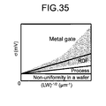
- the fluctuation of the Vth is considered to be based on in-plane fluctuation (in FIG. 35 , Non-uniformity in a wafer), fluctuation of processing size (in FIG. 35 , Process), and fluctuation of impurity concentration(in FIG. 35 , RDF).
- a metal electrode formed on a high-dielectric constant thin film comprising: a metal film containing a first electrode material; and a characteristic control film formed between the high-dielectric constant thin film and the metal film, the characteristic control film containing a second electrode material, wherein the metal electrode contains an element reducing a crystal grain diameter of the material constituting the metal film or the characteristic control film.
- a metal electrode as set forth in claim 1 of the present invention, wherein the element reducing the crystal grain diameter of the alloy is C, O, N, or Al.
- a metal electrode as set forth in claim 1 of the present invention, wherein a crystal structure of the characteristic control film is an fcc structure.
- a metal electrode as set forth in claim 1 of the present invention, wherein the first electrode material and the second electrode material are respectively selected from Ti, V, Cr, Zr, Nb, Mo, Hf, Ta, W, and nitrides thereof.
- a metal electrode as set forth in claim 1 of the present invention, wherein the characteristic control film contains a noble metal.
- a metal electrode as set forth in claim 1 of the present invention wherein the characteristic control film has a high concentration layer of the second electrode material; the high concentration layer is formed on a surface brought into contact with the high-dielectric constant thin film; and a concentration of the second electrode material in the high concentration layer is higher than an average concentration of the second electrode material in the whole characteristic control film.
- a metal electrode as set forth in claim 1 of the present invention wherein an average concentration of the second electrode material in the characteristic control film is 3 mol% to 40 mol%.
- a semiconductor element comprising the metal electrode according to any one of claims 1 to 7 used for an N channel.
- the metal electrode according to the present invention can control a work function and suppress fluctuation of a threshold voltage to control the threshold voltage.
- the present inventors examined a metal electrode used for a pair with a semiconductor so as to sandwich a high-dielectric constant thin film between the metal electrode and the semiconductor.
- the metal electrode includes a metal film containing a first electrode material and a characteristic control film containing a second electrode material and formed between the high-dielectric constant thin film and the metal film, and thereby a work function can be stabilized.
- the first electrode material contains W and TiN or the like as primary components. Polysilicon may be used for the first electrode material.
- a source 6 and a drain 7 are formed and separated a predetermined distance from each other on a silicon wafer 1 in a CMOS circuit as a semiconductor element according to the present embodiment. Impurities are implanted into the source 6 and the drain 7.
- a high-dielectric constant thin film 9 is provided on the silicon wafer 1 so as to cover the surface of the silicon wafer 1 between the source 6 and the drain 7.
- a metal electrode 13 is provided on the high-dielectric constant thin film 9.
- the metal electrode 13 includes a characteristic control film 10 containing the second electrode material, and a metal film 11 formed of the first electrode material.
- LDD side walls 5 are provided on the silicon wafer 1 so as to cover the both side surfaces of the high-dielectric constant thin film 9 thus formed and the both side surfaces of the metal electrode 13.
- the characteristic control film 10 contains, for example, Ru (band gap: 4.92 eV) as a noble metal which is a metal having a large work function, and Mo (band gap: 4.09 eV) as the second electrode material which is a metal having a small work function.
- the characteristic control film 10 has a Mo high concentration layer on a surface (hereinafter, may be referred to as " a boundary face") brought into contact with the high-dielectric constant thin film 9.
- the concentration of Mo in the high concentration layer is preferably adjusted so that the concentration of Mo is higher than the average concentration of Mo in the whole characteristic control film 10.
- the high-dielectric constant thin film 9 is, for example, an HfO 2 film, an HfSiON film, and an HfAlO 2 film or the like.
- the characteristic control film 10 is an alloy containing Ru and Mo. Thereby, active oxygen contained in Ru is combined with Mo to form a thin electrical insulation film containing Mo-O on the boundary face. The action of the electrical insulation film formed on the boundary face is assumed to be able to stabilize the work function. Thereby, the metal electrode 13 according to the present invention achieves the work function difference of about 0.69 eV. Therefore, when the metal electrode 13 is used for the CMOS circuit, the low power consumption and high performance of the CMOS circuit are achieved.
- the concentration of Mo in the characteristic control film 10 is 3 mol% to 40 mol%.
- Mo can be stably segregated on the boundary face, the stability of the work function is further enhanced.
- the present inventors found a phenomenon that Mo is spontaneously segregated on the boundary face by adding Mo in an amount of 3 mol% to 40 mol% to Ru. Therefore, since the high concentration layer of Mo can be formed on the boundary face without having a particular process for forming the high concentration layer of Mo on the boundary face, the manufacturing process is simplified.
- the concentration of Mo in the characteristic control film 10 is more preferably 10 mol% to 40 mol%.
- the metal electrode 13 according to the present invention is used for a pair with the silicon wafer 1 as the semiconductor so as to sandwich an oxide film between the metal electrode 13 and the silicon wafer 1.
- the metal electrode 13 has the characteristic control film 10 to which C (carbon) is added. Thereby, the orientation and grain diameter of a crystal structure can be controlled. Therefore, when the metal electrode 13 is used for the CMOS circuit, fluctuation of a Vth is suppressed and the Vth is stably controlled.
- the oxide film is the high-dielectric constant thin film 9.
- the metal electrode 13 according to the present invention includes the metal film 11 formed of the first electrode material, and the characteristic control film 10 containing, for example, Ru as the noble metal, and Mo as the second electrode material.
- the characteristic control film 10 is formed between the high-dielectric constant thin film 9 and the metal film 11. C is added to the characteristic control film 10. Thereby, the work function is stabilized, and the orientation and grain diameter of the crystal structure are controlled. Therefore, when the metal electrode 13 is used for the CMOS circuit, the low power consumption and high performance of the CMOS circuit are achieved.
- An element reducing the crystal grain diameter of the characteristic control film 10 is selected from elements having a small atomic radius, for example, O, N, or Al or the like besides C.
- the crystal grain diameter of the characteristic control film 10 can be reduced by adding the element to the characteristic control film 10.
- the element can be added to the characteristic control film 10 by sputtering simultaneously with the formation of the characteristic control film 10.
- the additive amount of the element is preferably about 5 mol% to 15 mol%.
- the crystal grain diameter of the characteristic control film 10 is reduced, for example, by adding C, the structure of the characteristic control film 10 is consequently changed to an amorphous structure.
- the crystal structure of the characteristic control film 10 is an fcc structure. It was apparent from the experiment that even if the crystal grain diameters of the first electrode material and the second electrode material constituting the metal electrode 13 are identical, the fcc structure of the characteristic control film 10 as the crystal structure reduces fluctuation of a threshold as compared to a bcc structure thereof.
- the present invention is not limited to the embodiment, and various modifications within the scope of the present invention are possible.
- the metal electrode according to the present invention is applied to a gate electrode of the CMOS circuit as the semiconductor element.
- the present invention is not limited thereto.
- the metal electrode according to the present invention may be applied to a gate of a CMOS logic circuit, a control gate of a flash memory, and a gate of DRAM.
- the metal electrode 13 constituted as described above can be used for various semiconductor elements, for example, a light emitting diode, a solar cell, a bipolar transistor, and a field effect transistor (FET) or the like.
- a light emitting diode for example, a solar cell, a bipolar transistor, and a field effect transistor (FET) or the like.
- FET field effect transistor
- the first electrode material and the second electrode material various materials can be considered.
- the first electrode material and the second electrode material can be respectively selected from high melting point metals such as Ti, V, Cr, Zr, Nb, Hf, Ta or W, or nitrides thereof besides Mo.
- the present invention is not limited thereto.
- the crystal grain diameter of the first material constituting the metal film 11 may be reduced by adding C to the metal film 11.
- a method for manufacturing the metal electrode in using the metal electrode for the CMOS circuit will be described.
- a method for manufacturing can be used, which includes a general transistor formation process and wiring formation process.
- the transistor formation process as a characteristic portion will be described below.
- a portion related to the manufacture of the metal electrode according to the present invention is not different in nMOS and pMOS. Therefore, the portion will be described in the following description without distinguishing between the nMOS and the pMOS.
- a gate last process finally forming the metal electrode will be described.
- An element isolation region (not shown) is formed on the silicon wafer 1, and a silicon oxide film 2 and a polysilicon film 3 are then formed.
- a dummy gate 4 is formed in an etching process ( FIG. 2 ). Ions are implanted with the dummy gate 4 as a mask, and annealing is performed ( FIG. 3 ).
- the LDD side walls 5 are formed, and ions are then implanted into portions which serve as the source 6 and the drain 7 ( FIG. 4 ).
- An interlayer insulation film 8 is formed, and the surface thereof is planarized by chemical mechanical polish (CMP) ( FIG. 5 (A) ).
- CMP chemical mechanical polish
- the dummy gate 4 is removed ( FIG. 5 (B) ).
- the dummy gate 4 and the silicon oxide film 2 are removed, and the high-dielectric constant thin film 9 is then formed.
- C is added by sputtering while forming the characteristic control film 10.
- C is an element reducing the crystal grain diameter of a material constituting the characteristic control film 10.
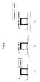
- the metal film 11 is sequentially formed to form the metal electrode 13 ( FIG. 6 ).
- Mo is segregated on the boundary face by performing annealing at about 450°C to form the high concentration layer (not shown) of Mo on the boundary face.
- the source 6 and the drain 7 are previously formed with the dummy gate 4 as the mask.
- the dummy gate 4 is removed, and the high-dielectric constant thin film 9 is deposited.
- the metal electrode 13 is produced. Thereby, since a low temperature process of 500°C or less can be achieved after forming the characteristic control film 10, the characteristic control film 10 to which C is added can be held in an amorphous state.
- a gate first process firstly forming the metal electrode will be described.
- the element isolation region (not shown) is formed on the silicon wafer 1.
- the high-dielectric constant thin film 9 is formed.
- C is then added by sputtering while forming the characteristic control film 10.
- C is an element reducing the crystal grain diameter of a material constituting the characteristic control film 10.
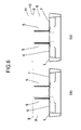
- the metal film 11 is sequentially formed to form the metal electrode 13 ( FIG. 7 ).
- Mo is segregated on the boundary face by performing annealing at about 450°C to form the high concentration layer of Mo (not shown) on the boundary face.
- ions are implanted, and annealing is performed ( FIG. 8 ).
- the side walls are formed, and ions are then implanted into portions which serve as the source 6 and the drain 7 ( FIG. 9 ).
- the interlayer insulation film 8 is formed, and the surface thereof is planarized by CMP ( FIG. 10 ).
- Example 1 a capacitor in which a characteristic control film was provided on a substrate was produced. The characteristics of a metal electrode according to the present invention were confirmed in the capacitor.
- a substrate having an HfSiON/SiO 2 /p-Si structure was used as a substrate on which the metal electrode according to the present invention was formed.
- HfSiON produced by an ALD (Atomic Layer Deposition)-CVD (Chemical Vapor Deposition) method was formed on an SiO 2 /p-Si structure.
- a characteristic control film to which C was added to a Ru-Mo alloy was deposited on the substrate by 60 nm using a stencil mask (metal mask) by the ALD-CVD method to produce a capacitor having a diameter of 100 ⁇ m.
- a continuous characteristic control film was also produced without using the stencil mask.
- the characteristic control film was also subjected to physical analyses such as X ray photoelectron spectrometry (XPS) and X-ray diffraction analysis (XRD).
- XPS X ray photoelectron spectrometry
- XRD X-ray diffraction analysis
- the characteristic control film was deposited at room temperature using an ion sputtering method and a magnetron sputtering method.
- a composition of the Ru-Mo alloy a thin film having a composition continuously changed from Ru (100 mol%) to Mo (100 mol%) was produced on a substrate using a technique (a combinatorial technique) for synthesizing a large number of compound groups (library) at the same time according to the combination.
- C was added in amounts of 1, 3, and 10 mol% to the film to form the characteristic control films.
- the capacitor was produced, and the capacitor was then annealed. C-V (capacity vs voltage) characteristics and I-V (current vs voltage) characteristics were measured.
- the annealing was performed in forming gas (FGA, in an atmosphere of 5% hydrogen and 95% nitrogen, 450°C) and in an oxygen environment (in an atmosphere of 1% oxygen and 99% nitrogen, 400°C to 800°C).
- FIGS. 11 to 20 show results obtained by confirming the characteristics of the characteristic control films produced as described above.
- FIG. 11 shows the measurement results of the XRD intensities of the characteristic control films annealed at 650°C. It was confirmed that the composition passes an amorphous state temporarily when the composition of the film is changed from pure Mo (100 mol%) to pure Ru (100 mol%).
- FIG. 12 shows two-dimensional XRD patterns. It was confirmed that a pure Mo film has a body-centred cubic lattice structure (bcc), and a pure Ru film has a face-centered cubic lattice structure (fcc).
- FIG. 13(A) shows a change in a Ru concentration based on a sputtering time for grinding the surface of the characteristic control film. From the results when sputtering is performed for 6 minutes and for 12 minutes in FIG. 13(A) , it can be confirmed that the Ru concentration is substantially in proportion to a position. However, from the result of no sputtering, it was confirmed that the increasing amount of the Ru concentration is reduced at a position of 4 to 6.5 mm, and Mo is stably segregated on the surface at a position in which the Ru concentration is 60 to 90%.
- FIG. 13(B) is an optical microscope photograph of the surface of the characteristic control film. In FIG. 13(B) , it was confirmed that Mo segregated on the surface appears brightly in a strip like shape.
- FIG. 14 shows the measurement results of XPS intensities before and after sputtering at a position of 5 mm (Ru concentration: 73.3 mol%) of FIG. 13(A) .
- a thin film including a bond of Mo-O is assumed to be formed on the boundary face between the Ru-Mo alloy and HfSiON.
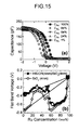
- FIG. 15(A) shows the results of C-V (capacity vs voltage) characteristics measured using the capacitor annealed at 600°C. Characteristically, the Ru concentration of 66 mol% appears on the leftmost side.
- a flat band voltage (V fb ) of a capacitor of SiO 2 (4 nm) was compared with a capacitor of HfSiON (4 nm)/SiO 2 (4 nm) ( FIG. 15(B) ).
- the flat band voltage means a gate voltage capable of planarizing the energy band of a semiconductor by applying a voltage to a gate electrode. In the capacitor of SiO 2 (4 nm), it is found that the flat band voltage difference between Mo and Ru is 0.78 V.
- the difference between work functions at this time is 0.83 eV.
- the flat band voltage when the Ru concentration is in the range of 60 mol% to 90 mol%, the flat band voltage is dramatically reduced.
- the flat band voltage when the Ru concentration is 60 mol% is -0.74 V, and is the same as that in the case of pure Mo.
- the capacitor of HfSiON (4 nm)/SiO 2 (4 nm) the flat band voltage difference between Mo and Ru is reduced to 0.47 V by a fermi level pinning phenomenon on the boundary face between the high-dielectric constant thin film and the metal electrode.
- FIG. 16 shows the relationship between the Ru concentration and the electrical insulation film.
- the electrical insulation film increases slightly. This means that an Mo oxide film is formed on the surface of a high-dielectric constant thin film.
- FIG. 17 shows a sectional image by a transmission electron microscope (TEM) of a capacitor of HfSiON (4 nm)/SiO 2 (4 nm).
- FIG. 17(A) shows a case where the characteristic control film is made of Ru 70 Mo 30 .
- FIG. 17(B) shows a case where the characteristic control film is made of pure Ru.
- a bright line (a portion enclosed with an ellipse of a white line in FIG.
- the thin Mo oxide film is considered to be formed of O atoms existing in a portion having a high concentration of Ru in the characteristic control film as shown in FIG. 18 .
- the thin Mo oxide film formed on HfSiON is believed to stabilize the flat band voltage. In actuality, it could be confirmed that the electrical insulation film is not increased in an electrode made of pure Mo ( FIG. 16 ).
- FIG. 19(A) shows the measurement results of XRD intensities obtained by observing Mo thin films (Ru concentration: 0 mol%) into which C is added in amounts of 0, 3, and 10 mol%. From FIG. 19(A) , peaks showing crystals are decreased. It was confirmed that a crystal size is reduced by adding C and the Mo thin film is changed to an amorphous state.
- FIG. 19(B) shows changes in sheet resistances of characteristic control films containing Ru and Mo when C is added into the characteristic control films. As is apparent from FIG. 19(B) , it is found that the addition of C and the change in the sheet resistance are also closely associated with a crystal structure.
- the sheet resistance is rapidly increased. This is because the crystal structure is changed to the amorphous state.
- the Ru concentration is 30 mol%, the sheet resistance is the almost same value regardless of the existence or nonexistence of the addition of C. This is because the characteristic control film is already in the amorphous state before C is added when the Ru concentration is 30 mol%, and the state is not changed even if C is added.
- FIG. 20 shows the measurement results of XRD intensities obtained by observing characteristic control films containing Ru and Mo immediately after forming the films.
- FIG. 20(A) shows the result when C is not added.
- FIG. 20(B) shows the result of the C concentration of about 1 mol%.
- the full width at half maximum (FWHM) of a peak shown by an arrow is increased in the total range of the Ru concentration. This shows that the crystal grain diameter is reduced.
- Example 2 it is confirmed that fluctuation of the Vth can be suppressed when the crystal grain diameter of an alloy of Ru and Mo in a metal electrode made of the alloy is reduced.
- a sample was produced using the alloy of Ru and Mo.
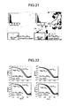
- FIG. 21(A) When an alloy is formed of Ru having an fcc structure as a crystal structure and Mo having a bcc structure, it was confirmed that a grain diameter size in a Ru 30 Mo 70 film is reduced ( FIG. 21(A) ).
- a rectangle in FIG. 21(A) has a size of 100 nm ⁇ 150 nm, and corresponds to a transistor size formed in the trial production.
- a crystal having an average grain diameter of 4 nm as a nanosize grain diameter could be confirmed in an amorphous base.
- a Ru 50 Mo 50 film FIG. 21(B)
- a crystal having a large grain diameter could be confirmed.
- a crystal having a large grain diameter of 100 nm or more could also be confirmed.
- Metal electrodes having gate lengths (Lg) of 1 ⁇ m and 130 nm were respectively formed of the Ru 30 Mo 70 film and the Ru 50 Mo 50 film.
- the Id-Vg characteristics thereof were measured ( FIG. 22 ).
- a transistor of HfSiON (2.5 nm)/SiO 2 (0.7 nm) was used as the high-dielectric constant thin film.
- a Vd (drain voltage) was -1.0 V, and substrate impurity concentrations were 6.0e17 cm -3 (High N sub in FIG. 22 ), and 2.7e17 cm -3 (Low N sub in FIG. 22 ). Thirty samples for each of the metal electrodes were measured. From this result, it was confirmed that the samples ( FIG.
- FIG. 23 shows the gate width dependence characteristics of Vth fluctuation.
- the sample is a metal electrode formed of the Ru 30 Mo 70 film and having a gate length of 150 nm. It could be confirmed that the Vth fluctuation is increased as the gate width (W) is reduced to 10 nm from 10 ⁇ m.
- FIG. 24 shows Pelgrom Plot of standard deviation ( ⁇ ) of a Vth (threshold) in a metal electrode formed of the Ru 30 Mo 70 film ( FIG. 24(A) ) and the Ru 50 Mo 50 film ( FIG. 24(B)).
- FIG. 24 shows that a value ⁇ of the metal electrode having a larger crystal grain diameter ( FIG. 24(B) ) is larger.
- the fluctuation of the Vth depends on the crystal grain diameter of the metal electrode, and the fluctuation of the Vth in the metal electrode having a smaller crystal grain diameter is smaller.
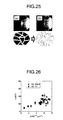
- FIG. 25 shows X-ray diffraction analysis (XRD) results of a Ru 50 Mo 50 film ( FIG. 25(A) ) and a film ( FIG. 25(b) ) in which C is added in an amount of 5 mol% to the Ru 50 Mo 50 film.
- XRD X-ray diffraction analysis
- FIG. 27 shows the difference of values ⁇ in a case of using a pair transistor formed of a Ru 50 Mo 50 film to which C is added in an amount of 5 mol% and a case of using an independent transistor.
- the difference of the values ⁇ in the case of using the independent transistor and the case of using the pair transistor is about 4 mV. In this experiment, it is found that the influence of in-plane fluctuation is small, and the experimental result ( FIG. 26 ) shows a significant difference.
- the metal electrode can be changed to the amorphous structure by adding C and the fluctuation of the Vth (threshold) can be reduced by using the metal electrode having the amorphous structure.
- FIG. 28 shows the relationship between a plane direction and a work function in metals (Pt, Pd, Ir, Au) having an fcc structure and metals (W, Ta, Nb, Mo) having a bcc structure (reference: H. B. Michaelson J. Appl. Phys. Vol. 48 (1977) 4729 .). Three samples were used for each of the metals. From FIG. 28 , it is confirmed that the work function is large in the bcc structure when the plane direction is a (100) plane, and the work function is large in the fcc structure when the plane direction is a (111) plane. It is shown that the plane direction dependence of the work function is high in the bcc structure.
- FIG. 29 shows the plane image by TEM, two-dimensional image by XRD, and histogram of pure Mo having the bcc structure and pure Ru having the fcc structure.
- a transistor of HfSiON (2.5 nm)/SiO 2 (0.7 nm) was used for the high-dielectric constant thin film.
- the film thickness of the pure Mo film or the pure Ru film as the characteristic control film formed on the high-dielectric constant thin film was set to 10 nm in any case.
- a W film was used as a metal film, and the film thickness thereof was set to 50 nm.
- FIG. 29 shows that a large number of small crystals gather in both pure Mo and pure Ru and size distributions are also similar to the histogram.
- a diffraction pattern drawing an arc shows that a crystal structure is a poly crystal structure.
- FIG. 30 shows the relationship between a gate width and ⁇ of a Vth in pure Mo having the bcc structure and pure Ru having the fcc structure. From FIG. 30 , it was confirmed that the value ⁇ of pure Mo having the bcc structure is 1.65 times larger than that of pure Ru having the fcc structure. Thereby, it was found that the fluctuation in the Vth is different based on the crystal structure even if the crystal grain diameter is almost the same, and the fluctuation of the fcc structure is smaller than that of the bcc structure. Therefore, it is considered that the fluctuation of the Vth can be further suppressed by using the material in which the crystal structure is the fcc structure.
- TiN is used as a characteristic control film
- the addition of C can reduce a crystal grain diameter, and the reduction can suppress fluctuation of a Vth.
- a transistor of HfSiON (2.5 nm)/SiO 2 (0.7 nm) was used as a high-dielectric constant thin film.
- the film thickness of a TiN film as the characteristic control film formed on the high-dielectric constant thin film was set to 5 to 30 nm.
- a W film was used as a metal film, and the film thickness thereof was set to 50 nm.
- FIG. 33 shows Pelgrom Plot in the TiN film and the TiN film to which C is added in an amount of 5 mol%. Measurements were performed according to a substrate impurity concentration. From FIG. 33 , the addition of C reduces the value ⁇ of the Vth, and the linearity is observed. From FIG. 34 , the substrate impurity concentration dependence of the value ⁇ of the Vth could be confirmed by using the TiN film to which C was added.
Landscapes
- Electrodes Of Semiconductors (AREA)
- Insulated Gate Type Field-Effect Transistor (AREA)
- Physical Vapour Deposition (AREA)
- Liquid Crystal (AREA)
- Semiconductor Integrated Circuits (AREA)
Abstract
Description
- The present invention relates to a metal electrode and a semiconductor element using the same. In particular, the present invention relates to a metal electrode formed on a high-dielectric constant thin film.
- A silicon oxide (SiO2) film has been used as a gate insulation film in, for example, a CMOS circuit as a semiconductor element. This gate insulation film is advanced in film thinning. Recently, the film thickness of the gate insulation film has been reduced to less than 1 nm. However, when the film thickness of the gate insulation film is reduced to the size of some atoms, a leak current is increased. Unfortunately, the increase of the leak current reduces reliability. A polysilicon film has been used for a gate electrode. However, the film thinning of the gate electrode increases a ratio of the film thickness of a depletion layer in the polysilicon film occupied in the film thickness of the gate electrode. Unfortunately, the increase of the ratio causes the reduction of a current driving force which cannot be disregarded.
- In order to solve such a problem, studies for replacing the silicon oxide film with a high dielectric constant (High-k) thin film to enhance the dielectric constant of the gate insulation film to increase the physical film thickness of the gate insulation film, or for replacing the polysilicon film with the metal electrode to suppress the depletion of the gate electrode have been actively performed.
- In this case, a method for controlling the threshold voltage of a device using respective two metals having a different work function for an electrode of an N channel and an electrode of a P channel makes the CMOS circuit operate (for example, Patent Document 1).
Patent Document 1 adjusts the film thickness of a layer made of a metallic material to be alloyed to adjust the gate electrode so as to have a suitable work function. - Patent Document 1: Japanese Patent Application Laid-Open No.
2006-199610 - However, when a metal is deposited on the high-dielectric constant thin film even in the
Patent Document 1, a gate electrode material and a gate insulation film material constituting the high-dielectric constant thin film react to unfortunately generate a phenomenon in which the effective work function of the gate electrode material is reduced (hereinafter, referred to as "a Fermi level pinning phenomenon"). Unfortunately, fluctuation of a threshold voltage (Vth) is larger. As shown inFIG. 35 , generally, the fluctuation of the Vth is considered to be based on in-plane fluctuation (inFIG. 35 , Non-uniformity in a wafer), fluctuation of processing size (inFIG. 35 , Process), and fluctuation of impurity concentration(inFIG. 35 , RDF). Since a more particular factor (inFIG. 35 , Metal gate) is further added in the case of the metal electrode, the fluctuation may become very large. Thus, it is unfortunately difficult to obtain a desired threshold voltage in the metal electrode formed on the high-dielectric constant thin film. - In the light of the aforementioned problems, it is an object of the present invention to provide a metal electrode capable of controlling a threshold voltage and formed on a high-dielectric constant thin film, and a semiconductor element using the metal electrode.
- In order to achieve the aforementioned object, in accordance with
claim 1 of the present invention, there is provided a metal electrode formed on a high-dielectric constant thin film, the metal electrode comprising: a metal film containing a first electrode material; and a characteristic control film formed between the high-dielectric constant thin film and the metal film, the characteristic control film containing a second electrode material, wherein the metal electrode contains an element reducing a crystal grain diameter of the material constituting the metal film or the characteristic control film. - In accordance with
claim 2 of the present invention, there is provided a metal electrode as set forth inclaim 1 of the present invention, wherein the element reducing the crystal grain diameter of the alloy is C, O, N, or Al. - In accordance with
claim 3 of the present invention, there is provided a metal electrode as set forth inclaim 1 of the present invention, wherein a crystal structure of the characteristic control film is an fcc structure. - In accordance with
claim 4 of the present invention, there is provided a metal electrode as set forth inclaim 1 of the present invention, wherein the first electrode material and the second electrode material are respectively selected from Ti, V, Cr, Zr, Nb, Mo, Hf, Ta, W, and nitrides thereof. - In accordance with
claim 5 of the present invention, there is provided a metal electrode as set forth inclaim 1 of the present invention, wherein the characteristic control film contains a noble metal. - In accordance with
claim 6 of the present invention, there is provided a metal electrode as set forth inclaim 1 of the present invention, wherein the characteristic control film has a high concentration layer of the second electrode material; the high concentration layer is formed on a surface brought into contact with the high-dielectric constant thin film; and a concentration of the second electrode material in the high concentration layer is higher than an average concentration of the second electrode material in the whole characteristic control film. - In accordance with
claim 7 of the present invention, there is provided a metal electrode as set forth inclaim 1 of the present invention, wherein an average concentration of the second electrode material in the characteristic control film is 3 mol% to 40 mol%. - In accordance with
claim 8 of the present invention, there is provided a semiconductor element comprising the metal electrode according to any one ofclaims 1 to 7 used for an N channel. - The metal electrode according to the present invention can control a work function and suppress fluctuation of a threshold voltage to control the threshold voltage.
-
-
FIG. 1 is a sectional view of a CMOS circuit using a metal electrode according to the present invention. -
FIG. 2 shows a manufacturing process by a gate last process of the CMOS circuit using the metal electrode according to the present invention, and shows the manufacturing process after dummy gate etching. -
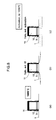
FIG. 3 shows the manufacturing process by the gate last process of the CMOS circuit using the metal electrode,FIG. 3(A) showing anneal,FIG. 3(B) showing ion implantation,FIG. 3(C) showing anneal. -
FIG. 4 shows the manufacturing process by the gate last process of the CMOS circuit using the metal electrode,FIG. 4(A) showing the formation of side walls,FIG. 4(B) showing ion implantation to a drain and a source. -
FIG. 5 shows the manufacturing process by the gate last process of the CMOS circuit using the metal electrode,FIG. 5(A) showing the formation of an interlayer insulation film,FIG. 5(B) showing the removal of a dummy gate. -
FIG. 6 shows the manufacturing process by the gate last process of the CMOS circuit using the metal electrode,FIG. 6(A) showing the formation of a high-dielectric constant thin film,FIG. 6(B) showing the formation of a characteristic control film and a metal film. -
FIG. 7 shows the manufacturing process by the gate first process of the CMOS circuit using the metal electrode according to the present invention, and shows the manufacturing process after gate etching. -
FIG. 8 shows the manufacturing process by the gate first process of the CMOS circuit using the metal electrode,FIG. 8(A) showing anneal,FIG. 8(B) showing ion implantation,FIG. 8(C) showing anneal. -
FIG. 9 shows the manufacturing process by the gate first process of the CMOS circuit using the metal electrode,FIG. 9(A) showing the formation of LDD side walls,FIG. 9(B) showing ion implantation to a drain and a source. -
FIG. 10 shows the manufacturing process by the gate first process of the CMOS circuit using the metal electrode, and shows the formation of an interlayer insulation film. -
FIG. 11 shows the results of examples, and shows the measurement results of the XRD intensities of characteristic control films annealed at 650°C. -
FIG. 12 shows the results of Example 1, and shows two-dimensional XRD patterns. -
FIG. 13 shows the results of Example 1,FIG. 13(A) showing a change in a Ru concentration based on a sputtering time,FIG. 13(B) being a photograph obtained by imaging the surface of the characteristic control film by an optical microscope. -
FIG. 14 shows the results of Example 1, and shows the measurement results of XPS intensities before and after sputtering at a position of 5 mm ofFIG. 13(A) . -
FIG. 15 shows the results of Example 1,FIG. 15(A) showing the results of C-V (capacity vs voltage) characteristics measured using the capacitor annealed at 600°C,FIG. 15(B) showing a flat band voltage to the Ru concentration. -
FIG. 16 shows the results of Example 1, and shows the relationship between the Ru concentration and an electrical insulation film. -
FIG. 17 shows the results of Example 1, and shows a sectional image by a transmission electron microscope (TEM) of a capacitor of HfSiON (4 nm)/SiO2 (4 nm),FIG. 17(A) showing a case where a characteristic control film is made of Ru70Mo30,FIG. 17(B) showing a case where a characteristic control film is made of pure Ru. -
FIG. 18 schematically shows the relationship of Mo, Ru and HfSiON,FIG. 18(A) showing a case where the characteristic control film is made of pure Mo,FIG. 18(B) showing a case where the characteristic control film is made of Ru70Mo30,FIG. 18(C) showing a case where the characteristic control film is made of pure Ru. -
FIG. 19 shows the results of Example 1,FIG. 19(A) showing the measurement results of XRD intensities obtained by observing Mo thin films (Ru concentration: 0 mol%) into which C is added in amounts of 0, 3, and 10 mol%,FIG. 19(B) showing changes in sheet resistances of characteristic control films containing Ru and Mo when C is added into the characteristic control films. -
FIG. 20 shows the results of Example 1, and shows the measurement results of XRD intensities obtained by observing characteristic control films containing Ru and Mo of as-depo,FIG. 20(A) showing the result when C is not added,FIG. 20(B) showing the result of the C concentration of about 1 mol%. -
FIG. 21 shows plane images by a TEM showing the results of Example 2 and grain diameter size distributions,FIG. 21(A) showing a Ru30Mo70 film,FIG. 21(B) showing a Ru50Mo50 film. -
FIG. 22 shows Id-Vg characteristics showing the results of Example 2,FIG. 22(A) using a metal electrode produced by a Ru30Mo70 film and having a gate length of 1 µm,FIG. 22(B) using a metal electrode produced by a Ru50Mo50 film and having a gate length of 1 µm,FIG. 22(C) using a metal electrode produced by a Ru30Mo70 film and having a gate length of 130 nm,FIG. 22(B) using a metal electrode produced by a Ru50Mo50 film and having a gate length of 130 nm. -
FIG. 23 shows the results of Example 2, and shows gate width dependence of fluctuation of a Vth. -
FIG. 24 shows Pelgrom Plot of standard deviation (σ) of a Vth (threshold) in a metal electrode showing the results of Example 2,FIG. 24(A) using a Ru30Mo70 film,FIG. 24(B) using a Ru50Mo50 film. -
FIG. 25 shows a two-dimensional image by XRD showing the results of Example 3,FIG. 25(A) showing a Ru50Mo50 film at an upper side,FIG. 25(B) showing a film in which C is added to Ru50Mo50 at an upper side,FIGS. 25(A), 25(B) showing an effect obtained by adding C at respective lower sides. -
FIG. 26 shows Pelgrom Plot of standard deviation (σ) of a Vth (threshold) in a metal electrode formed of a film in which C is added to Ru50Mo50 showing the results of Example 3. -
FIG. 27 shows the results of Example 3, and shows the difference of values σ in a case of using a pair transistor formed of a Ru50Mo50 film to which C is added and a case of using an independent transistor. -
FIG. 28 shows the results of Example 4, and shows the relationship between a plane direction and a work function in a metal having an fcc structure and a metal having a bcc structure. -
FIG. 29 shows a plane image by TEM, a two-dimensional image by XRD, and a histogram which show the results of Example 4,FIG. 29(A) showing pure Mo having a bcc structure,FIG. 29(B) showing pure Ru having an fcc structure. -
FIG. 30 shows the results of Example 4, and shows the relationship between the gate widths of pure Mo and pure Ru, and σ□ -
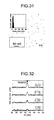
FIG. 31 shows the results of Example 5, and shows a plane image by TEM of a TiN film and a grain diameter size distribution. -
FIG. 32 shows the results of Example 5, and shows XRD spectra of a TiN film having added C. -
FIG. 33 shows Pelgrom Plot showing the results of Example 5,FIG. 33(A) showing a case of using a TiN film,FIG. 33(B) showing a case of using a TiNC film. -
FIG. 34 shows the results of Example 5, and shows substrate concentration dependence of inclination inFIG. 33 . -
FIG. 35 schematically shows a factor of fluctuation of a Vth in the combination of a high-dielectric constant thin film and a metal electrode. - The present inventors examined a metal electrode used for a pair with a semiconductor so as to sandwich a high-dielectric constant thin film between the metal electrode and the semiconductor. As a result, the present inventors found that the metal electrode includes a metal film containing a first electrode material and a characteristic control film containing a second electrode material and formed between the high-dielectric constant thin film and the metal film, and thereby a work function can be stabilized. It is preferable that the first electrode material contains W and TiN or the like as primary components. Polysilicon may be used for the first electrode material.
- As shown in
FIG. 1 , asource 6 and adrain 7 are formed and separated a predetermined distance from each other on asilicon wafer 1 in a CMOS circuit as a semiconductor element according to the present embodiment. Impurities are implanted into thesource 6 and thedrain 7. A high-dielectric constantthin film 9 is provided on thesilicon wafer 1 so as to cover the surface of thesilicon wafer 1 between thesource 6 and thedrain 7. Ametal electrode 13 is provided on the high-dielectric constantthin film 9. Themetal electrode 13 includes acharacteristic control film 10 containing the second electrode material, and ametal film 11 formed of the first electrode material. Furthermore,LDD side walls 5 are provided on thesilicon wafer 1 so as to cover the both side surfaces of the high-dielectric constantthin film 9 thus formed and the both side surfaces of themetal electrode 13. - That is, the
characteristic control film 10 according to the present invention contains, for example, Ru (band gap: 4.92 eV) as a noble metal which is a metal having a large work function, and Mo (band gap: 4.09 eV) as the second electrode material which is a metal having a small work function. Thecharacteristic control film 10 has a Mo high concentration layer on a surface (hereinafter, may be referred to as " a boundary face") brought into contact with the high-dielectric constantthin film 9. Herein, the concentration of Mo in the high concentration layer is preferably adjusted so that the concentration of Mo is higher than the average concentration of Mo in the wholecharacteristic control film 10. The high-dielectric constantthin film 9 is, for example, an HfO2 film, an HfSiON film, and an HfAlO2 film or the like. Thecharacteristic control film 10 is an alloy containing Ru and Mo. Thereby, active oxygen contained in Ru is combined with Mo to form a thin electrical insulation film containing Mo-O on the boundary face. The action of the electrical insulation film formed on the boundary face is assumed to be able to stabilize the work function. Thereby, themetal electrode 13 according to the present invention achieves the work function difference of about 0.69 eV. Therefore, when themetal electrode 13 is used for the CMOS circuit, the low power consumption and high performance of the CMOS circuit are achieved. - In the
metal electrode 13 according to the present invention, the concentration of Mo in thecharacteristic control film 10 is 3 mol% to 40 mol%. Thereby, since Mo can be stably segregated on the boundary face, the stability of the work function is further enhanced. The present inventors found a phenomenon that Mo is spontaneously segregated on the boundary face by adding Mo in an amount of 3 mol% to 40 mol% to Ru. Therefore, since the high concentration layer of Mo can be formed on the boundary face without having a particular process for forming the high concentration layer of Mo on the boundary face, the manufacturing process is simplified. The concentration of Mo in thecharacteristic control film 10 is more preferably 10 mol% to 40 mol%. - The
metal electrode 13 according to the present invention is used for a pair with thesilicon wafer 1 as the semiconductor so as to sandwich an oxide film between themetal electrode 13 and thesilicon wafer 1. Themetal electrode 13 has thecharacteristic control film 10 to which C (carbon) is added. Thereby, the orientation and grain diameter of a crystal structure can be controlled. Therefore, when themetal electrode 13 is used for the CMOS circuit, fluctuation of a Vth is suppressed and the Vth is stably controlled. - The oxide film is the high-dielectric constant
thin film 9. Themetal electrode 13 according to the present invention includes themetal film 11 formed of the first electrode material, and thecharacteristic control film 10 containing, for example, Ru as the noble metal, and Mo as the second electrode material. Thecharacteristic control film 10 is formed between the high-dielectric constantthin film 9 and themetal film 11. C is added to thecharacteristic control film 10. Thereby, the work function is stabilized, and the orientation and grain diameter of the crystal structure are controlled. Therefore, when themetal electrode 13 is used for the CMOS circuit, the low power consumption and high performance of the CMOS circuit are achieved. - An element reducing the crystal grain diameter of the
characteristic control film 10 is selected from elements having a small atomic radius, for example, O, N, or Al or the like besides C. The crystal grain diameter of thecharacteristic control film 10 can be reduced by adding the element to thecharacteristic control film 10. The element can be added to thecharacteristic control film 10 by sputtering simultaneously with the formation of thecharacteristic control film 10. The additive amount of the element is preferably about 5 mol% to 15 mol%. As the crystal grain diameter of thecharacteristic control film 10 is reduced, for example, by adding C, the structure of thecharacteristic control film 10 is consequently changed to an amorphous structure. - It is preferable that the crystal structure of the
characteristic control film 10 is an fcc structure. It was apparent from the experiment that even if the crystal grain diameters of the first electrode material and the second electrode material constituting themetal electrode 13 are identical, the fcc structure of thecharacteristic control film 10 as the crystal structure reduces fluctuation of a threshold as compared to a bcc structure thereof. - The present invention is not limited to the embodiment, and various modifications within the scope of the present invention are possible. For example, in the embodiment, the case where the metal electrode according to the present invention is applied to a gate electrode of the CMOS circuit as the semiconductor element is described. However, the present invention is not limited thereto. The metal electrode according to the present invention may be applied to a gate of a CMOS logic circuit, a control gate of a flash memory, and a gate of DRAM.
- The
metal electrode 13 constituted as described above can be used for various semiconductor elements, for example, a light emitting diode, a solar cell, a bipolar transistor, and a field effect transistor (FET) or the like. - As the first electrode material and the second electrode material, various materials can be considered. The first electrode material and the second electrode material can be respectively selected from high melting point metals such as Ti, V, Cr, Zr, Nb, Hf, Ta or W, or nitrides thereof besides Mo.
- In the embodiment, the case where, for example, C is added to the
characteristic control film 10 is described. However, the present invention is not limited thereto. The crystal grain diameter of the first material constituting themetal film 11 may be reduced by adding C to themetal film 11. - Next, a method for manufacturing the metal electrode in using the metal electrode for the CMOS circuit will be described. In manufacturing the CMOS circuit using the metal electrode according to the present invention, a method for manufacturing can be used, which includes a general transistor formation process and wiring formation process. The transistor formation process as a characteristic portion will be described below. In the transistor formation process, a portion related to the manufacture of the metal electrode according to the present invention is not different in nMOS and pMOS. Therefore, the portion will be described in the following description without distinguishing between the nMOS and the pMOS.
- First, a gate last process finally forming the metal electrode will be described. An element isolation region (not shown) is formed on the
silicon wafer 1, and asilicon oxide film 2 and apolysilicon film 3 are then formed. Then, adummy gate 4 is formed in an etching process (FIG. 2 ). Ions are implanted with thedummy gate 4 as a mask, and annealing is performed (FIG. 3 ). - The
LDD side walls 5 are formed, and ions are then implanted into portions which serve as thesource 6 and the drain 7 (FIG. 4 ). Aninterlayer insulation film 8 is formed, and the surface thereof is planarized by chemical mechanical polish (CMP) (FIG. 5 (A) ). Then, thedummy gate 4 is removed (FIG. 5 (B) ). Thedummy gate 4 and thesilicon oxide film 2 are removed, and the high-dielectric constantthin film 9 is then formed. Then, after the high-dielectric constantthin film 9 is formed, C is added by sputtering while forming thecharacteristic control film 10. C is an element reducing the crystal grain diameter of a material constituting thecharacteristic control film 10. Then, themetal film 11 is sequentially formed to form the metal electrode 13 (FIG. 6 ). In thecharacteristic control film 10 formed on the high-dielectric constantthin film 9, Mo is segregated on the boundary face by performing annealing at about 450°C to form the high concentration layer (not shown) of Mo on the boundary face. - Thus, the
source 6 and thedrain 7 are previously formed with thedummy gate 4 as the mask. Thedummy gate 4 is removed, and the high-dielectric constantthin film 9 is deposited. Then, themetal electrode 13 is produced. Thereby, since a low temperature process of 500°C or less can be achieved after forming thecharacteristic control film 10, thecharacteristic control film 10 to which C is added can be held in an amorphous state. - Next, a gate first process firstly forming the metal electrode will be described. The element isolation region (not shown) is formed on the
silicon wafer 1. Then, the high-dielectric constantthin film 9 is formed. C is then added by sputtering while forming thecharacteristic control film 10. C is an element reducing the crystal grain diameter of a material constituting thecharacteristic control film 10. Then, themetal film 11 is sequentially formed to form the metal electrode 13 (FIG. 7 ). In thecharacteristic control film 10 formed on the high-dielectric constantthin film 9, Mo is segregated on the boundary face by performing annealing at about 450°C to form the high concentration layer of Mo (not shown) on the boundary face. - Then, ions are implanted, and annealing is performed (
FIG. 8 ). The side walls are formed, and ions are then implanted into portions which serve as thesource 6 and the drain 7 (FIG. 9 ). Theinterlayer insulation film 8 is formed, and the surface thereof is planarized by CMP (FIG. 10 ). - Hereinafter, Examples will be described. In Example 1, a capacitor in which a characteristic control film was provided on a substrate was produced. The characteristics of a metal electrode according to the present invention were confirmed in the capacitor.
- A substrate having an HfSiON/SiO2/p-Si structure was used as a substrate on which the metal electrode according to the present invention was formed. In the substrate having the HfSiON/SiO2/p-Si structure, HfSiON produced by an ALD (Atomic Layer Deposition)-CVD (Chemical Vapor Deposition) method was formed on an SiO2/p-Si structure. A characteristic control film to which C was added to a Ru-Mo alloy was deposited on the substrate by 60 nm using a stencil mask (metal mask) by the ALD-CVD method to produce a capacitor having a diameter of 100 µm. A continuous characteristic control film was also produced without using the stencil mask. The characteristic control film was also subjected to physical analyses such as X ray photoelectron spectrometry (XPS) and X-ray diffraction analysis (XRD).
- The characteristic control film was deposited at room temperature using an ion sputtering method and a magnetron sputtering method. As for the composition of the Ru-Mo alloy, a thin film having a composition continuously changed from Ru (100 mol%) to Mo (100 mol%) was produced on a substrate using a technique (a combinatorial technique) for synthesizing a large number of compound groups (library) at the same time according to the combination. C was added in amounts of 1, 3, and 10 mol% to the film to form the characteristic control films.
- The capacitor was produced, and the capacitor was then annealed. C-V (capacity vs voltage) characteristics and I-V (current vs voltage) characteristics were measured. The annealing was performed in forming gas (FGA, in an atmosphere of 5% hydrogen and 95% nitrogen, 450°C) and in an oxygen environment (in an atmosphere of 1% oxygen and 99% nitrogen, 400°C to 800°C).
-
FIGS. 11 to 20 show results obtained by confirming the characteristics of the characteristic control films produced as described above.FIG. 11 shows the measurement results of the XRD intensities of the characteristic control films annealed at 650°C. It was confirmed that the composition passes an amorphous state temporarily when the composition of the film is changed from pure Mo (100 mol%) to pure Ru (100 mol%).FIG. 12 shows two-dimensional XRD patterns. It was confirmed that a pure Mo film has a body-centred cubic lattice structure (bcc), and a pure Ru film has a face-centered cubic lattice structure (fcc). -
FIG. 13(A) shows a change in a Ru concentration based on a sputtering time for grinding the surface of the characteristic control film. From the results when sputtering is performed for 6 minutes and for 12 minutes inFIG. 13(A) , it can be confirmed that the Ru concentration is substantially in proportion to a position. However, from the result of no sputtering, it was confirmed that the increasing amount of the Ru concentration is reduced at a position of 4 to 6.5 mm, and Mo is stably segregated on the surface at a position in which the Ru concentration is 60 to 90%.FIG. 13(B) is an optical microscope photograph of the surface of the characteristic control film. InFIG. 13(B) , it was confirmed that Mo segregated on the surface appears brightly in a strip like shape. -
FIG. 14 shows the measurement results of XPS intensities before and after sputtering at a position of 5 mm (Ru concentration: 73.3 mol%) ofFIG. 13(A) . A peak existing before sputtering and showing the existence of Mo-O of about 223 eV disappears after sputtering. A thin film including a bond of Mo-O is assumed to be formed on the boundary face between the Ru-Mo alloy and HfSiON. -
FIG. 15(A) shows the results of C-V (capacity vs voltage) characteristics measured using the capacitor annealed at 600°C. Characteristically, the Ru concentration of 66 mol% appears on the leftmost side. A flat band voltage (Vfb) of a capacitor of SiO2 (4 nm) was compared with a capacitor of HfSiON (4 nm)/SiO2 (4 nm) (FIG. 15(B) ). The flat band voltage means a gate voltage capable of planarizing the energy band of a semiconductor by applying a voltage to a gate electrode. In the capacitor of SiO2 (4 nm), it is found that the flat band voltage difference between Mo and Ru is 0.78 V. The difference between work functions at this time is 0.83 eV. However, when the Ru concentration is in the range of 60 mol% to 90 mol%, the flat band voltage is dramatically reduced. The flat band voltage when the Ru concentration is 60 mol% is -0.74 V, and is the same as that in the case of pure Mo. On the other hand, in the capacitor of HfSiON (4 nm)/SiO2 (4 nm), the flat band voltage difference between Mo and Ru is reduced to 0.47 V by a fermi level pinning phenomenon on the boundary face between the high-dielectric constant thin film and the metal electrode. In the capacitor of HfSiON (4 nm)/SiO2 (4 nm), it was confirmed that the flat band voltage is stable when the Ru concentration is in the range of 60 mol% to 90 mol%. Thereby, the flat band voltage when the Ru concentration is in the range of 60 mol% to 90 mol% is lower than the flat band in pure Mo. As a result, it was confirmed that the work function difference of 0.69 eV can be achieved in an HfSiON(4 nm)/SiO2 (4 nm) structure. -
FIG. 16 shows the relationship between the Ru concentration and the electrical insulation film. When the Ru concentration is in the range of 60 mol% to 90 mol%, the electrical insulation film increases slightly. This means that an Mo oxide film is formed on the surface of a high-dielectric constant thin film.FIG. 17 shows a sectional image by a transmission electron microscope (TEM) of a capacitor of HfSiON (4 nm)/SiO2 (4 nm).FIG. 17(A) shows a case where the characteristic control film is made of Ru70Mo30.FIG. 17(B) shows a case where the characteristic control film is made of pure Ru. A bright line (a portion enclosed with an ellipse of a white line inFIG. 17(A) ) considered as the Mo oxide film is observed only in the characteristic control film made of Ru70Mo30. The thin Mo oxide film is considered to be formed of O atoms existing in a portion having a high concentration of Ru in the characteristic control film as shown inFIG. 18 . The thin Mo oxide film formed on HfSiON is believed to stabilize the flat band voltage. In actuality, it could be confirmed that the electrical insulation film is not increased in an electrode made of pure Mo (FIG. 16 ). -
FIG. 19(A) shows the measurement results of XRD intensities obtained by observing Mo thin films (Ru concentration: 0 mol%) into which C is added in amounts of 0, 3, and 10 mol%. FromFIG. 19(A) , peaks showing crystals are decreased. It was confirmed that a crystal size is reduced by adding C and the Mo thin film is changed to an amorphous state.FIG. 19(B) shows changes in sheet resistances of characteristic control films containing Ru and Mo when C is added into the characteristic control films. As is apparent fromFIG. 19(B) , it is found that the addition of C and the change in the sheet resistance are also closely associated with a crystal structure. For example, when the Ru concentration is 0 mol% and the C concentration is increased to 10 mol% from 3 mol%, the sheet resistance is rapidly increased. This is because the crystal structure is changed to the amorphous state. When the Ru concentration is 30 mol%, the sheet resistance is the almost same value regardless of the existence or nonexistence of the addition of C. This is because the characteristic control film is already in the amorphous state before C is added when the Ru concentration is 30 mol%, and the state is not changed even if C is added. -
FIG. 20 shows the measurement results of XRD intensities obtained by observing characteristic control films containing Ru and Mo immediately after forming the films.FIG. 20(A) shows the result when C is not added.FIG. 20(B) shows the result of the C concentration of about 1 mol%. InFIG. 20(B) , the full width at half maximum (FWHM) of a peak shown by an arrow is increased in the total range of the Ru concentration. This shows that the crystal grain diameter is reduced. - In Example 2, it is confirmed that fluctuation of the Vth can be suppressed when the crystal grain diameter of an alloy of Ru and Mo in a metal electrode made of the alloy is reduced. First, a sample was produced using the alloy of Ru and Mo.
- When an alloy is formed of Ru having an fcc structure as a crystal structure and Mo having a bcc structure, it was confirmed that a grain diameter size in a Ru30Mo70 film is reduced (
FIG. 21(A) ). A rectangle inFIG. 21(A) has a size of 100 nm × 150 nm, and corresponds to a transistor size formed in the trial production. In the Ru30Mo70 film, a crystal having an average grain diameter of 4 nm as a nanosize grain diameter could be confirmed in an amorphous base. On the other hand, in a Ru50Mo50 film (FIG. 21(B) ), a crystal having a large grain diameter could be confirmed. In particular, in the upper right ofFIG. 21(B) , as surrounded by a line, a crystal having a large grain diameter of 100 nm or more could also be confirmed. - Metal electrodes having gate lengths (Lg) of 1 µm and 130 nm were respectively formed of the Ru30Mo70 film and the Ru50Mo50 film. The Id-Vg characteristics thereof were measured (
FIG. 22 ). A transistor of HfSiON (2.5 nm)/SiO2 (0.7 nm) was used as the high-dielectric constant thin film. A Vd (drain voltage) was -1.0 V, and substrate impurity concentrations were 6.0e17 cm-3 (High Nsub inFIG. 22 ), and 2.7e17 cm-3 (Low Nsub inFIG. 22 ). Thirty samples for each of the metal electrodes were measured. From this result, it was confirmed that the samples (FIG. 22(A), (C) ) having a smaller crystal grain diameter have smaller fluctuation of the Id-Vg characteristics. In the samples (FIG. 22(B), (D) ) having a larger crystal grain diameter, it was shown that fluctuation in the Id-Vg characteristics is larger in a particularly small device (FIG. 22(D) ). -
FIG. 23 shows the gate width dependence characteristics of Vth fluctuation. The sample is a metal electrode formed of the Ru30Mo70 film and having a gate length of 150 nm. It could be confirmed that the Vth fluctuation is increased as the gate width (W) is reduced to 10 nm from 10 µm. -
FIG. 24 shows Pelgrom Plot of standard deviation (σ) of a Vth (threshold) in a metal electrode formed of the Ru30Mo70 film (FIG. 24(A) ) and the Ru50Mo50 film (FIG. 24(B)). FIG. 24 shows that a value σ of the metal electrode having a larger crystal grain diameter (FIG. 24(B) ) is larger. - As described above, it could be confirmed that the fluctuation of the Vth depends on the crystal grain diameter of the metal electrode, and the fluctuation of the Vth in the metal electrode having a smaller crystal grain diameter is smaller.
- Then, it is confirmed that the addition of C can change the structure of the metal electrode to an amorphous structure and can reduce the fluctuation of the Vth.
-
FIG. 25 shows X-ray diffraction analysis (XRD) results of a Ru50Mo50 film (FIG. 25(A) ) and a film (FIG. 25(b) ) in which C is added in an amount of 5 mol% to the Ru50Mo50 film. InFIG. 25(A) , a sharp intensity distribution can be confirmed. This shows high crystallinity. On the other hand, inFIG. 25(B) , an amorphous structure can be confirmed. Therefore, in the Ru50Mo50 film, it could be confirmed that the structure of the film is changed to the amorphous structure by adding C. - Furthermore, Pelgrom Plot of σ of a Vth in a Ru50Mo50 film to which C is added in an amount of 5 mol% is shown (
FIG. 26 ). It could be confirmed that the value σ□ of the amorphous structure formed by adding C is reduced as compared withFIG. 24(B) of the Ru50Mo50 film to which C is not added. -
FIG. 27 shows the difference of values σ in a case of using a pair transistor formed of a Ru50Mo50 film to which C is added in an amount of 5 mol% and a case of using an independent transistor. The difference of the values σ in the case of using the independent transistor and the case of using the pair transistor is about 4 mV. In this experiment, it is found that the influence of in-plane fluctuation is small, and the experimental result (FIG. 26 ) shows a significant difference. - As described above, it could be confirmed that the metal electrode can be changed to the amorphous structure by adding C and the fluctuation of the Vth (threshold) can be reduced by using the metal electrode having the amorphous structure.
- Next, when the crystal structure of the characteristic control film is an fcc structure, it is confirmed that the fluctuation of the Vth is reduced.
- First,
FIG. 28 shows the relationship between a plane direction and a work function in metals (Pt, Pd, Ir, Au) having an fcc structure and metals (W, Ta, Nb, Mo) having a bcc structure (reference: H. B. Michaelson J. Appl. Phys. Vol. 48 (1977) 4729.). Three samples were used for each of the metals. FromFIG. 28 , it is confirmed that the work function is large in the bcc structure when the plane direction is a (100) plane, and the work function is large in the fcc structure when the plane direction is a (111) plane. It is shown that the plane direction dependence of the work function is high in the bcc structure. -
FIG. 29 shows the plane image by TEM, two-dimensional image by XRD, and histogram of pure Mo having the bcc structure and pure Ru having the fcc structure. A transistor of HfSiON (2.5 nm)/SiO2 (0.7 nm) was used for the high-dielectric constant thin film. The film thickness of the pure Mo film or the pure Ru film as the characteristic control film formed on the high-dielectric constant thin film was set to 10 nm in any case. Furthermore, a W film was used as a metal film, and the film thickness thereof was set to 50 nm.FIG. 29 shows that a large number of small crystals gather in both pure Mo and pure Ru and size distributions are also similar to the histogram. In the two-dimensional image by XRD, a diffraction pattern drawing an arc shows that a crystal structure is a poly crystal structure. -
FIG. 30 shows the relationship between a gate width and σ of a Vth in pure Mo having the bcc structure and pure Ru having the fcc structure. FromFIG. 30 , it was confirmed that the value σ of pure Mo having the bcc structure is 1.65 times larger than that of pure Ru having the fcc structure. Thereby, it was found that the fluctuation in the Vth is different based on the crystal structure even if the crystal grain diameter is almost the same, and the fluctuation of the fcc structure is smaller than that of the bcc structure. Therefore, it is considered that the fluctuation of the Vth can be further suppressed by using the material in which the crystal structure is the fcc structure. - Next, when TiN is used as a characteristic control film, it is confirmed that the addition of C can reduce a crystal grain diameter, and the reduction can suppress fluctuation of a Vth. A transistor of HfSiON (2.5 nm)/SiO2 (0.7 nm) was used as a high-dielectric constant thin film. The film thickness of a TiN film as the characteristic control film formed on the high-dielectric constant thin film was set to 5 to 30 nm. Furthermore, a W film was used as a metal film, and the film thickness thereof was set to 50 nm.
- From a plane image by TEM (
FIG. 31 ) of the TiN film, it could be confirmed that the TiN film has a small average grain diameter of 4.3 nm. However, from XRD spectrum when C is added to the TiN film shown inFIG. 32 , it could be confirmed that the intensity of a XRD peak is reduced with the increase in the C concentration. This shows that the addition of C can further reduce the size and/or density of the crystal. -
FIG. 33 shows Pelgrom Plot in the TiN film and the TiN film to which C is added in an amount of 5 mol%. Measurements were performed according to a substrate impurity concentration. FromFIG. 33 , the addition of C reduces the value σ of the Vth, and the linearity is observed. FromFIG. 34 , the substrate impurity concentration dependence of the value σ of the Vth could be confirmed by using the TiN film to which C was added. - As described above, it has been confirmed that the addition of C can reduce the crystal grain diameter even when TiN is used as the characteristic control film, and thereby the fluctuation of the Vth can be suppressed. Furthermore, the substrate impurity concentration dependence of the value σ of the Vth could be confirmed in the TiN film to which C was added.
Claims (8)
- A metal electrode formed on a high-dielectric constant thin film, the metal electrode comprising:a metal film containing a first electrode material; anda characteristic control film formed between the high-dielectric constant thin film and the metal film, the characteristic control film containing a second electrode material,wherein the metal electrode contains an element reducing a crystal grain diameter of the material constituting the metal film or the characteristic control film.
- The metal electrode according to claim 1, wherein the element is C, O, N, or Al.
- The metal electrode according to claim 1, wherein a crystal structure of the characteristic control film is an fcc structure.
- The metal electrode according to claim 1, wherein the first electrode material and the second electrode material are respectively selected from Ti, V, Cr, Zr, Nb, Mo, Hf, Ta, W, and nitrides thereof.
- The metal electrode according to claim 1, wherein the characteristic control film contains a noble metal.
- The metal electrode according to claim 1, wherein the characteristic control film has a high concentration layer of the second electrode material; the high concentration layer is formed on a surface brought into contact with the high-dielectric constant thin film; and a concentration of the second electrode material in the high concentration layer is higher than an average concentration of the second electrode material in the whole characteristic control film.
- The metal electrode according to claim 1, wherein an average concentration of the second electrode material in the characteristic control film is 3 mol% to 40 mol%.
- A semiconductor element comprising the metal electrode according to any one of claims 1 to 7 used for an N channel.
Applications Claiming Priority (2)
| Application Number | Priority Date | Filing Date | Title |
|---|---|---|---|
| JP2007317614 | 2007-12-07 | ||
| PCT/JP2008/072164 WO2009072611A1 (en) | 2007-12-07 | 2008-12-05 | Metal electrode and semiconductor element using the same |
Publications (3)
| Publication Number | Publication Date |
|---|---|
| EP2237320A1 true EP2237320A1 (en) | 2010-10-06 |
| EP2237320A4 EP2237320A4 (en) | 2011-11-16 |
| EP2237320B1 EP2237320B1 (en) | 2014-03-19 |
Family
ID=40717789
Family Applications (1)
| Application Number | Title | Priority Date | Filing Date |
|---|---|---|---|
| EP08858001.4A Not-in-force EP2237320B1 (en) | 2007-12-07 | 2008-12-05 | Metal electrode and semiconductor element using the same |
Country Status (5)
| Country | Link |
|---|---|
| US (1) | US20110204520A1 (en) |
| EP (1) | EP2237320B1 (en) |
| JP (2) | JP5414053B2 (en) |
| TW (1) | TW200937632A (en) |
| WO (1) | WO2009072611A1 (en) |
Families Citing this family (1)
| Publication number | Priority date | Publication date | Assignee | Title |
|---|---|---|---|---|
| CN104183475B (en) * | 2013-05-21 | 2016-12-28 | 中芯国际集成电路制造(上海)有限公司 | Grid structure and forming method thereof |
Family Cites Families (21)
| Publication number | Priority date | Publication date | Assignee | Title |
|---|---|---|---|---|
| JP3523093B2 (en) * | 1997-11-28 | 2004-04-26 | 株式会社東芝 | Semiconductor device and manufacturing method thereof |
| US6846739B1 (en) * | 1998-02-27 | 2005-01-25 | Micron Technology, Inc. | MOCVD process using ozone as a reactant to deposit a metal oxide barrier layer |
| US6228512B1 (en) * | 1999-05-26 | 2001-05-08 | The Regents Of The University Of California | MoRu/Be multilayers for extreme ultraviolet applications |
| JP3771801B2 (en) * | 2001-01-16 | 2006-04-26 | 株式会社ルネサステクノロジ | Semiconductor device |
| CN100517422C (en) * | 2002-03-07 | 2009-07-22 | 三洋电机株式会社 | Distributing structure, its manufacturing method and optical equipment |
| JP4301784B2 (en) * | 2002-08-30 | 2009-07-22 | シャープ株式会社 | Method for producing laminated electrode on p-type group III nitride semiconductor contact layer and p-type laminated electrode |
| JP2004134705A (en) * | 2002-10-15 | 2004-04-30 | Jiaotong Univ | Metal oxide semiconductor field effect transistor and its gate structure |
| JP2004349595A (en) * | 2003-05-26 | 2004-12-09 | Sharp Corp | Nitride semiconductor laser device and method of manufacturing the same |
| US7030430B2 (en) * | 2003-08-15 | 2006-04-18 | Intel Corporation | Transition metal alloys for use as a gate electrode and devices incorporating these alloys |
| US7029966B2 (en) * | 2003-09-18 | 2006-04-18 | International Business Machines Corporation | Process options of forming silicided metal gates for advanced CMOS devices |
| US7064050B2 (en) * | 2003-11-28 | 2006-06-20 | International Business Machines Corporation | Metal carbide gate structure and method of fabrication |
| JP2005285809A (en) * | 2004-03-26 | 2005-10-13 | Sony Corp | Semiconductor device and manufacturing method thereof |
| US7592678B2 (en) * | 2004-06-17 | 2009-09-22 | Infineon Technologies Ag | CMOS transistors with dual high-k gate dielectric and methods of manufacture thereof |
| CN101019225B (en) * | 2004-08-24 | 2011-01-26 | Nxp股份有限公司 | Semiconductor device and method of manufacturing such a semiconductor device |
| JP4533155B2 (en) * | 2005-01-12 | 2010-09-01 | 富士通セミコンダクター株式会社 | Semiconductor device and manufacturing method thereof |
| JP2006199610A (en) | 2005-01-19 | 2006-08-03 | Kao Corp | Wrinkle-improving agent |
| JP2007005721A (en) * | 2005-06-27 | 2007-01-11 | Toshiba Corp | Semiconductor device and manufacturing method thereof |
| JP4220509B2 (en) * | 2005-09-06 | 2009-02-04 | 株式会社ルネサステクノロジ | Manufacturing method of semiconductor device |
| US7291527B2 (en) * | 2005-09-07 | 2007-11-06 | Texas Instruments Incorporated | Work function control of metals |
| JP2007134650A (en) * | 2005-11-14 | 2007-05-31 | Toshiba Corp | Semiconductor device and manufacturing method thereof |
| JP5197986B2 (en) * | 2007-04-06 | 2013-05-15 | ルネサスエレクトロニクス株式会社 | Semiconductor device manufacturing equipment |
-
2008
- 2008-12-05 US US12/746,621 patent/US20110204520A1/en not_active Abandoned
- 2008-12-05 EP EP08858001.4A patent/EP2237320B1/en not_active Not-in-force
- 2008-12-05 JP JP2009544742A patent/JP5414053B2/en not_active Expired - Fee Related
- 2008-12-05 WO PCT/JP2008/072164 patent/WO2009072611A1/en not_active Ceased
- 2008-12-08 TW TW097147624A patent/TW200937632A/en unknown
-
2013
- 2013-09-27 JP JP2013201187A patent/JP5704546B2/en not_active Expired - Fee Related
Non-Patent Citations (2)
| Title |
|---|
| LI ET AL: "Forming gas anneal induced flat-band voltage shift of metal-oxide-semiconductor stacks and its link with hydrogen incorporation in metal gates", MICROELECTRONIC ENGINEERING, ELSEVIER PUBLISHERS BV., AMSTERDAM, NL, vol. 84, no. 9-10, 30 May 2007 (2007-05-30), pages 2213-2216, XP022097272, ISSN: 0167-9317, DOI: 10.1016/J.MEE.2007.04.106 * |
| See also references of WO2009072611A1 * |
Also Published As
| Publication number | Publication date |
|---|---|
| JP5414053B2 (en) | 2014-02-12 |
| EP2237320A4 (en) | 2011-11-16 |
| JPWO2009072611A1 (en) | 2011-04-28 |
| WO2009072611A1 (en) | 2009-06-11 |
| JP5704546B2 (en) | 2015-04-22 |
| US20110204520A1 (en) | 2011-08-25 |
| EP2237320B1 (en) | 2014-03-19 |
| JP2014039051A (en) | 2014-02-27 |
| TW200937632A (en) | 2009-09-01 |
Similar Documents
| Publication | Publication Date | Title |
|---|---|---|
| US9391091B2 (en) | MOSFET with work function adjusted metal backgate | |
| CN110911492B (en) | Electronic device and method of manufacturing the same | |
| US7023064B2 (en) | Temperature stable metal nitride gate electrode | |
| US7091568B2 (en) | Electronic device including dielectric layer, and a process for forming the electronic device | |
| US11832458B2 (en) | Tunable doping of carbon nanotubes through engineered atomic layer deposition | |
| US20050104142A1 (en) | CVD tantalum compounds for FET get electrodes | |
| US20090114995A1 (en) | Complementary semiconductor device and method of manufacturing the same | |
| US20090134465A1 (en) | Semiconductor structure | |
| KR20120068738A (en) | Semiconductor device and manufacturing method thereof | |
| JP2004214673A (en) | Use of indium to determine the work function of p-doped polysilicon or polysilicon germanium | |
| US12477810B2 (en) | Semiconductor device and manufacturing method thereof | |
| US9859157B1 (en) | Method for forming improved liner layer and semiconductor device including the same | |
| US20120045892A1 (en) | Method for fabricating semiconductor device | |
| US7511338B2 (en) | Semiconductor device and manufacturing method of the same | |
| Lee et al. | Graded crystalline HfO₂ gate dielectric layer for high-k/Ge MOS gate stack | |
| US20090283836A1 (en) | Cmos structure including protective spacers and method of forming thereof | |
| JP2007027500A (en) | Semiconductor device and manufacturing method thereof | |
| EP2237320B1 (en) | Metal electrode and semiconductor element using the same | |
| US20160181109A1 (en) | Semiconductor device manufacturing method | |
| US7786537B2 (en) | Semiconductor device and method for manufacturing same | |
| EP1389799A1 (en) | Method for production of a layered structure with nanocrystals in a dielectric layer | |
| Maheshwari et al. | Trends and Challenges in VLSI Fabrication Technology | |
| US20070267706A1 (en) | Formation of low leakage thermally assisted radical nitrided dielectrics | |
| Ťapajna et al. | Work function thermal stability of RuO2-rich Ru–Si–O p-channel metal-oxide-semiconductor field-effect transistor gate electrodes | |
| US7872328B2 (en) | Capacitor electrode that contains oxygen and nitrogen |
Legal Events
| Date | Code | Title | Description |
|---|---|---|---|
| PUAI | Public reference made under article 153(3) epc to a published international application that has entered the european phase |
Free format text: ORIGINAL CODE: 0009012 |
|
| 17P | Request for examination filed |
Effective date: 20100705 |
|
| AK | Designated contracting states |
Kind code of ref document: A1 Designated state(s): AT BE BG CH CY CZ DE DK EE ES FI FR GB GR HR HU IE IS IT LI LT LU LV MC MT NL NO PL PT RO SE SI SK TR |
|
| AX | Request for extension of the european patent |
Extension state: AL BA MK RS |
|
| DAX | Request for extension of the european patent (deleted) | ||
| A4 | Supplementary search report drawn up and despatched |
Effective date: 20111017 |
|
| RIC1 | Information provided on ipc code assigned before grant |
Ipc: H01L 21/336 20060101ALI20111011BHEP Ipc: H01L 27/092 20060101ALI20111011BHEP Ipc: H01L 29/423 20060101ALI20111011BHEP Ipc: H01L 21/28 20060101ALI20111011BHEP Ipc: H01L 27/088 20060101ALI20111011BHEP Ipc: H01L 29/78 20060101AFI20111011BHEP Ipc: H01L 21/8238 20060101ALI20111011BHEP Ipc: H01L 29/49 20060101ALI20111011BHEP Ipc: H01L 29/51 20060101ALN20111011BHEP Ipc: H01L 21/8234 20060101ALI20111011BHEP |
|
| 17Q | First examination report despatched |
Effective date: 20120713 |
|
| GRAP | Despatch of communication of intention to grant a patent |
Free format text: ORIGINAL CODE: EPIDOSNIGR1 |
|
| RIC1 | Information provided on ipc code assigned before grant |
Ipc: H01L 21/28 20060101ALI20130124BHEP Ipc: H01L 27/088 20060101ALI20130124BHEP Ipc: H01L 29/78 20060101AFI20130124BHEP Ipc: H01L 27/092 20060101ALI20130124BHEP Ipc: H01L 29/49 20060101ALI20130124BHEP Ipc: H01L 21/336 20060101ALI20130124BHEP Ipc: H01L 21/8234 20060101ALI20130124BHEP Ipc: H01L 29/423 20060101ALI20130124BHEP Ipc: H01L 21/8238 20060101ALI20130124BHEP Ipc: H01L 29/51 20060101ALN20130124BHEP |
|
| RIC1 | Information provided on ipc code assigned before grant |
Ipc: H01L 29/423 20060101ALI20130211BHEP Ipc: H01L 21/28 20060101ALI20130211BHEP Ipc: H01L 27/092 20060101ALI20130211BHEP Ipc: H01L 21/8234 20060101ALI20130211BHEP Ipc: H01L 29/51 20060101ALN20130211BHEP Ipc: H01L 21/8238 20060101ALI20130211BHEP Ipc: H01L 29/49 20060101ALI20130211BHEP Ipc: H01L 21/336 20060101ALI20130211BHEP Ipc: H01L 29/78 20060101AFI20130211BHEP Ipc: H01L 27/088 20060101ALI20130211BHEP |
|
| RIC1 | Information provided on ipc code assigned before grant |
Ipc: H01L 27/088 20060101ALI20130904BHEP Ipc: H01L 29/423 20060101ALI20130904BHEP Ipc: H01L 29/49 20060101ALI20130904BHEP Ipc: H01L 21/8234 20060101ALI20130904BHEP Ipc: H01L 27/092 20060101ALI20130904BHEP Ipc: H01L 29/78 20060101AFI20130904BHEP Ipc: H01L 21/28 20060101ALI20130904BHEP Ipc: H01L 29/51 20060101ALN20130904BHEP Ipc: H01L 21/8238 20060101ALI20130904BHEP Ipc: H01L 21/336 20060101ALI20130904BHEP |
|
| GRAP | Despatch of communication of intention to grant a patent |
Free format text: ORIGINAL CODE: EPIDOSNIGR1 |
|
| INTG | Intention to grant announced |
Effective date: 20131030 |
|
| GRAS | Grant fee paid |
Free format text: ORIGINAL CODE: EPIDOSNIGR3 |
|
| GRAA | (expected) grant |
Free format text: ORIGINAL CODE: 0009210 |
|
| AK | Designated contracting states |
Kind code of ref document: B1 Designated state(s): AT BE BG CH CY CZ DE DK EE ES FI FR GB GR HR HU IE IS IT LI LT LU LV MC MT NL NO PL PT RO SE SI SK TR |
|
| REG | Reference to a national code |
Ref country code: GB Ref legal event code: FG4D |
|
| REG | Reference to a national code |
Ref country code: CH Ref legal event code: EP |
|
| REG | Reference to a national code |
Ref country code: IE Ref legal event code: FG4D |
|
| REG | Reference to a national code |
Ref country code: AT Ref legal event code: REF Ref document number: 658156 Country of ref document: AT Kind code of ref document: T Effective date: 20140415 |
|
| REG | Reference to a national code |
Ref country code: DE Ref legal event code: R096 Ref document number: 602008031015 Country of ref document: DE Effective date: 20140430 |
|
| PG25 | Lapsed in a contracting state [announced via postgrant information from national office to epo] |
Ref country code: LT Free format text: LAPSE BECAUSE OF FAILURE TO SUBMIT A TRANSLATION OF THE DESCRIPTION OR TO PAY THE FEE WITHIN THE PRESCRIBED TIME-LIMIT Effective date: 20140319 Ref country code: NO Free format text: LAPSE BECAUSE OF FAILURE TO SUBMIT A TRANSLATION OF THE DESCRIPTION OR TO PAY THE FEE WITHIN THE PRESCRIBED TIME-LIMIT Effective date: 20140619 |
|
| REG | Reference to a national code |
Ref country code: NL Ref legal event code: VDEP Effective date: 20140319 |
|
| REG | Reference to a national code |
Ref country code: AT Ref legal event code: MK05 Ref document number: 658156 Country of ref document: AT Kind code of ref document: T Effective date: 20140319 |
|
| REG | Reference to a national code |
Ref country code: LT Ref legal event code: MG4D |
|
| PG25 | Lapsed in a contracting state [announced via postgrant information from national office to epo] |
Ref country code: SE Free format text: LAPSE BECAUSE OF FAILURE TO SUBMIT A TRANSLATION OF THE DESCRIPTION OR TO PAY THE FEE WITHIN THE PRESCRIBED TIME-LIMIT Effective date: 20140319 Ref country code: FI Free format text: LAPSE BECAUSE OF FAILURE TO SUBMIT A TRANSLATION OF THE DESCRIPTION OR TO PAY THE FEE WITHIN THE PRESCRIBED TIME-LIMIT Effective date: 20140319 Ref country code: CY Free format text: LAPSE BECAUSE OF FAILURE TO SUBMIT A TRANSLATION OF THE DESCRIPTION OR TO PAY THE FEE WITHIN THE PRESCRIBED TIME-LIMIT Effective date: 20140319 |
|
| PG25 | Lapsed in a contracting state [announced via postgrant information from national office to epo] |
Ref country code: HR Free format text: LAPSE BECAUSE OF FAILURE TO SUBMIT A TRANSLATION OF THE DESCRIPTION OR TO PAY THE FEE WITHIN THE PRESCRIBED TIME-LIMIT Effective date: 20140319 Ref country code: LV Free format text: LAPSE BECAUSE OF FAILURE TO SUBMIT A TRANSLATION OF THE DESCRIPTION OR TO PAY THE FEE WITHIN THE PRESCRIBED TIME-LIMIT Effective date: 20140319 |
|
| PG25 | Lapsed in a contracting state [announced via postgrant information from national office to epo] |
Ref country code: IS Free format text: LAPSE BECAUSE OF FAILURE TO SUBMIT A TRANSLATION OF THE DESCRIPTION OR TO PAY THE FEE WITHIN THE PRESCRIBED TIME-LIMIT Effective date: 20140719 Ref country code: RO Free format text: LAPSE BECAUSE OF FAILURE TO SUBMIT A TRANSLATION OF THE DESCRIPTION OR TO PAY THE FEE WITHIN THE PRESCRIBED TIME-LIMIT Effective date: 20140319 Ref country code: NL Free format text: LAPSE BECAUSE OF FAILURE TO SUBMIT A TRANSLATION OF THE DESCRIPTION OR TO PAY THE FEE WITHIN THE PRESCRIBED TIME-LIMIT Effective date: 20140319 Ref country code: BG Free format text: LAPSE BECAUSE OF FAILURE TO SUBMIT A TRANSLATION OF THE DESCRIPTION OR TO PAY THE FEE WITHIN THE PRESCRIBED TIME-LIMIT Effective date: 20140619 Ref country code: CZ Free format text: LAPSE BECAUSE OF FAILURE TO SUBMIT A TRANSLATION OF THE DESCRIPTION OR TO PAY THE FEE WITHIN THE PRESCRIBED TIME-LIMIT Effective date: 20140319 Ref country code: EE Free format text: LAPSE BECAUSE OF FAILURE TO SUBMIT A TRANSLATION OF THE DESCRIPTION OR TO PAY THE FEE WITHIN THE PRESCRIBED TIME-LIMIT Effective date: 20140319 |
|
| PG25 | Lapsed in a contracting state [announced via postgrant information from national office to epo] |
Ref country code: AT Free format text: LAPSE BECAUSE OF FAILURE TO SUBMIT A TRANSLATION OF THE DESCRIPTION OR TO PAY THE FEE WITHIN THE PRESCRIBED TIME-LIMIT Effective date: 20140319 Ref country code: SK Free format text: LAPSE BECAUSE OF FAILURE TO SUBMIT A TRANSLATION OF THE DESCRIPTION OR TO PAY THE FEE WITHIN THE PRESCRIBED TIME-LIMIT Effective date: 20140319 Ref country code: ES Free format text: LAPSE BECAUSE OF FAILURE TO SUBMIT A TRANSLATION OF THE DESCRIPTION OR TO PAY THE FEE WITHIN THE PRESCRIBED TIME-LIMIT Effective date: 20140319 Ref country code: PL Free format text: LAPSE BECAUSE OF FAILURE TO SUBMIT A TRANSLATION OF THE DESCRIPTION OR TO PAY THE FEE WITHIN THE PRESCRIBED TIME-LIMIT Effective date: 20140319 |
|
| REG | Reference to a national code |
Ref country code: DE Ref legal event code: R097 Ref document number: 602008031015 Country of ref document: DE |
|
| PG25 | Lapsed in a contracting state [announced via postgrant information from national office to epo] |
Ref country code: PT Free format text: LAPSE BECAUSE OF FAILURE TO SUBMIT A TRANSLATION OF THE DESCRIPTION OR TO PAY THE FEE WITHIN THE PRESCRIBED TIME-LIMIT Effective date: 20140721 |
|
| PLBE | No opposition filed within time limit |
Free format text: ORIGINAL CODE: 0009261 |
|
| STAA | Information on the status of an ep patent application or granted ep patent |
Free format text: STATUS: NO OPPOSITION FILED WITHIN TIME LIMIT |
|
| PG25 | Lapsed in a contracting state [announced via postgrant information from national office to epo] |
Ref country code: DK Free format text: LAPSE BECAUSE OF FAILURE TO SUBMIT A TRANSLATION OF THE DESCRIPTION OR TO PAY THE FEE WITHIN THE PRESCRIBED TIME-LIMIT Effective date: 20140319 |
|
| 26N | No opposition filed |
Effective date: 20141222 |
|
| PG25 | Lapsed in a contracting state [announced via postgrant information from national office to epo] |
Ref country code: IT Free format text: LAPSE BECAUSE OF FAILURE TO SUBMIT A TRANSLATION OF THE DESCRIPTION OR TO PAY THE FEE WITHIN THE PRESCRIBED TIME-LIMIT Effective date: 20140319 |
|
| REG | Reference to a national code |
Ref country code: DE Ref legal event code: R097 Ref document number: 602008031015 Country of ref document: DE Effective date: 20141222 |
|
| REG | Reference to a national code |
Ref country code: DE Ref legal event code: R119 Ref document number: 602008031015 Country of ref document: DE |
|
| PG25 | Lapsed in a contracting state [announced via postgrant information from national office to epo] |
Ref country code: LU Free format text: LAPSE BECAUSE OF FAILURE TO SUBMIT A TRANSLATION OF THE DESCRIPTION OR TO PAY THE FEE WITHIN THE PRESCRIBED TIME-LIMIT Effective date: 20141205 Ref country code: SI Free format text: LAPSE BECAUSE OF FAILURE TO SUBMIT A TRANSLATION OF THE DESCRIPTION OR TO PAY THE FEE WITHIN THE PRESCRIBED TIME-LIMIT Effective date: 20140319 |
|
| REG | Reference to a national code |
Ref country code: CH Ref legal event code: PL |
|
| GBPC | Gb: european patent ceased through non-payment of renewal fee |
Effective date: 20141205 |
|
| REG | Reference to a national code |
Ref country code: IE Ref legal event code: MM4A |
|
| PG25 | Lapsed in a contracting state [announced via postgrant information from national office to epo] |
Ref country code: IE Free format text: LAPSE BECAUSE OF NON-PAYMENT OF DUE FEES Effective date: 20141205 Ref country code: CH Free format text: LAPSE BECAUSE OF NON-PAYMENT OF DUE FEES Effective date: 20141231 Ref country code: LI Free format text: LAPSE BECAUSE OF NON-PAYMENT OF DUE FEES Effective date: 20141231 Ref country code: GB Free format text: LAPSE BECAUSE OF NON-PAYMENT OF DUE FEES Effective date: 20141205 Ref country code: DE Free format text: LAPSE BECAUSE OF NON-PAYMENT OF DUE FEES Effective date: 20150701 |
|
| REG | Reference to a national code |
Ref country code: FR Ref legal event code: PLFP Year of fee payment: 8 |
|
| PGFP | Annual fee paid to national office [announced via postgrant information from national office to epo] |
Ref country code: FR Payment date: 20151221 Year of fee payment: 8 Ref country code: BE Payment date: 20151221 Year of fee payment: 8 |
|
| PG25 | Lapsed in a contracting state [announced via postgrant information from national office to epo] |
Ref country code: MC Free format text: LAPSE BECAUSE OF FAILURE TO SUBMIT A TRANSLATION OF THE DESCRIPTION OR TO PAY THE FEE WITHIN THE PRESCRIBED TIME-LIMIT Effective date: 20140319 |
|
| PG25 | Lapsed in a contracting state [announced via postgrant information from national office to epo] |
Ref country code: GR Free format text: LAPSE BECAUSE OF FAILURE TO SUBMIT A TRANSLATION OF THE DESCRIPTION OR TO PAY THE FEE WITHIN THE PRESCRIBED TIME-LIMIT Effective date: 20140620 |
|
| PG25 | Lapsed in a contracting state [announced via postgrant information from national office to epo] |
Ref country code: TR Free format text: LAPSE BECAUSE OF FAILURE TO SUBMIT A TRANSLATION OF THE DESCRIPTION OR TO PAY THE FEE WITHIN THE PRESCRIBED TIME-LIMIT Effective date: 20140319 Ref country code: HU Free format text: LAPSE BECAUSE OF FAILURE TO SUBMIT A TRANSLATION OF THE DESCRIPTION OR TO PAY THE FEE WITHIN THE PRESCRIBED TIME-LIMIT; INVALID AB INITIO Effective date: 20081205 Ref country code: MT Free format text: LAPSE BECAUSE OF FAILURE TO SUBMIT A TRANSLATION OF THE DESCRIPTION OR TO PAY THE FEE WITHIN THE PRESCRIBED TIME-LIMIT Effective date: 20140319 |
|
| PG25 | Lapsed in a contracting state [announced via postgrant information from national office to epo] |
Ref country code: BE Free format text: LAPSE BECAUSE OF NON-PAYMENT OF DUE FEES Effective date: 20161231 |
|
| REG | Reference to a national code |
Ref country code: FR Ref legal event code: ST Effective date: 20170831 |
|
| PG25 | Lapsed in a contracting state [announced via postgrant information from national office to epo] |
Ref country code: FR Free format text: LAPSE BECAUSE OF NON-PAYMENT OF DUE FEES Effective date: 20170102 |
|
| REG | Reference to a national code |
Ref country code: BE Ref legal event code: MM Effective date: 20161231 |