EP2237309A2 - Apparatus for chemically etching a workpiece - Google Patents
Apparatus for chemically etching a workpiece Download PDFInfo
- Publication number
- EP2237309A2 EP2237309A2 EP10154656A EP10154656A EP2237309A2 EP 2237309 A2 EP2237309 A2 EP 2237309A2 EP 10154656 A EP10154656 A EP 10154656A EP 10154656 A EP10154656 A EP 10154656A EP 2237309 A2 EP2237309 A2 EP 2237309A2
- Authority
- EP
- European Patent Office
- Prior art keywords
- chamber
- window
- pumping port
- sub
- workpiece
- Prior art date
- Legal status (The legal status is an assumption and is not a legal conclusion. Google has not performed a legal analysis and makes no representation as to the accuracy of the status listed.)
- Granted
Links
Images


Classifications
-
- C—CHEMISTRY; METALLURGY
- C23—COATING METALLIC MATERIAL; COATING MATERIAL WITH METALLIC MATERIAL; CHEMICAL SURFACE TREATMENT; DIFFUSION TREATMENT OF METALLIC MATERIAL; COATING BY VACUUM EVAPORATION, BY SPUTTERING, BY ION IMPLANTATION OR BY CHEMICAL VAPOUR DEPOSITION, IN GENERAL; INHIBITING CORROSION OF METALLIC MATERIAL OR INCRUSTATION IN GENERAL
- C23F—NON-MECHANICAL REMOVAL OF METALLIC MATERIAL FROM SURFACE; INHIBITING CORROSION OF METALLIC MATERIAL OR INCRUSTATION IN GENERAL; MULTI-STEP PROCESSES FOR SURFACE TREATMENT OF METALLIC MATERIAL INVOLVING AT LEAST ONE PROCESS PROVIDED FOR IN CLASS C23 AND AT LEAST ONE PROCESS COVERED BY SUBCLASS C21D OR C22F OR CLASS C25
- C23F1/00—Etching metallic material by chemical means
- C23F1/08—Apparatus, e.g. for photomechanical printing surfaces
-
- H—ELECTRICITY
- H10—SEMICONDUCTOR DEVICES; ELECTRIC SOLID-STATE DEVICES NOT OTHERWISE PROVIDED FOR
- H10P—GENERIC PROCESSES OR APPARATUS FOR THE MANUFACTURE OR TREATMENT OF DEVICES COVERED BY CLASS H10
- H10P72/00—Handling or holding of wafers, substrates or devices during manufacture or treatment thereof
- H10P72/06—Apparatus for monitoring, sorting, marking, testing or measuring
- H10P72/0604—Process monitoring, e.g. flow or thickness monitoring
-
- C—CHEMISTRY; METALLURGY
- C23—COATING METALLIC MATERIAL; COATING MATERIAL WITH METALLIC MATERIAL; CHEMICAL SURFACE TREATMENT; DIFFUSION TREATMENT OF METALLIC MATERIAL; COATING BY VACUUM EVAPORATION, BY SPUTTERING, BY ION IMPLANTATION OR BY CHEMICAL VAPOUR DEPOSITION, IN GENERAL; INHIBITING CORROSION OF METALLIC MATERIAL OR INCRUSTATION IN GENERAL
- C23F—NON-MECHANICAL REMOVAL OF METALLIC MATERIAL FROM SURFACE; INHIBITING CORROSION OF METALLIC MATERIAL OR INCRUSTATION IN GENERAL; MULTI-STEP PROCESSES FOR SURFACE TREATMENT OF METALLIC MATERIAL INVOLVING AT LEAST ONE PROCESS PROVIDED FOR IN CLASS C23 AND AT LEAST ONE PROCESS COVERED BY SUBCLASS C21D OR C22F OR CLASS C25
- C23F1/00—Etching metallic material by chemical means
- C23F1/10—Etching compositions
- C23F1/12—Gaseous compositions
-
- C—CHEMISTRY; METALLURGY
- C23—COATING METALLIC MATERIAL; COATING MATERIAL WITH METALLIC MATERIAL; CHEMICAL SURFACE TREATMENT; DIFFUSION TREATMENT OF METALLIC MATERIAL; COATING BY VACUUM EVAPORATION, BY SPUTTERING, BY ION IMPLANTATION OR BY CHEMICAL VAPOUR DEPOSITION, IN GENERAL; INHIBITING CORROSION OF METALLIC MATERIAL OR INCRUSTATION IN GENERAL
- C23F—NON-MECHANICAL REMOVAL OF METALLIC MATERIAL FROM SURFACE; INHIBITING CORROSION OF METALLIC MATERIAL OR INCRUSTATION IN GENERAL; MULTI-STEP PROCESSES FOR SURFACE TREATMENT OF METALLIC MATERIAL INVOLVING AT LEAST ONE PROCESS PROVIDED FOR IN CLASS C23 AND AT LEAST ONE PROCESS COVERED BY SUBCLASS C21D OR C22F OR CLASS C25
- C23F4/00—Processes for removing metallic material from surfaces, not provided for in group C23F1/00 or C23F3/00
- C23F4/02—Processes for removing metallic material from surfaces, not provided for in group C23F1/00 or C23F3/00 by evaporation
-
- H—ELECTRICITY
- H01—ELECTRIC ELEMENTS
- H01J—ELECTRIC DISCHARGE TUBES OR DISCHARGE LAMPS
- H01J37/00—Discharge tubes with provision for introducing objects or material to be exposed to the discharge, e.g. for the purpose of examination or processing thereof
- H01J37/32—Gas-filled discharge tubes
- H01J37/32917—Plasma diagnostics
- H01J37/32935—Monitoring and controlling tubes by information coming from the object and/or discharge
- H01J37/32963—End-point detection
-
- H—ELECTRICITY
- H01—ELECTRIC ELEMENTS
- H01J—ELECTRIC DISCHARGE TUBES OR DISCHARGE LAMPS
- H01J37/00—Discharge tubes with provision for introducing objects or material to be exposed to the discharge, e.g. for the purpose of examination or processing thereof
- H01J37/32—Gas-filled discharge tubes
- H01J37/32917—Plasma diagnostics
- H01J37/32935—Monitoring and controlling tubes by information coming from the object and/or discharge
- H01J37/32972—Spectral analysis
-
- H—ELECTRICITY
- H01—ELECTRIC ELEMENTS
- H01J—ELECTRIC DISCHARGE TUBES OR DISCHARGE LAMPS
- H01J37/00—Discharge tubes with provision for introducing objects or material to be exposed to the discharge, e.g. for the purpose of examination or processing thereof
- H01J37/32—Gas-filled discharge tubes
- H01J37/32917—Plasma diagnostics
- H01J37/32935—Monitoring and controlling tubes by information coming from the object and/or discharge
- H01J37/32981—Gas analysis
-
- H—ELECTRICITY
- H01—ELECTRIC ELEMENTS
- H01J—ELECTRIC DISCHARGE TUBES OR DISCHARGE LAMPS
- H01J37/00—Discharge tubes with provision for introducing objects or material to be exposed to the discharge, e.g. for the purpose of examination or processing thereof
- H01J37/32—Gas-filled discharge tubes
- H01J37/32917—Plasma diagnostics
- H01J37/3299—Feedback systems
Definitions
- This invention relates to apparatus and methods for chemically etching a workpiece using a process gas.
- the invention consists in apparatus for chemically etching a workpiece using a process gas, the apparatus including a chamber for receiving a process gas and having a pumping port for extracting exhaust gases; and a workpiece support located in the chamber upstream of the pumping port characterised in that the chamber further includes a sub-chamber located upstream of the pumping port and downstream of the workpiece support and in that the sub-chamber includes a window and an excitation source, adjacent the window, for creating a plasma in a sample of the exhaust gases to create an optical emission which can be monitored through the window.
- the sub-chamber may include an extension or dead end in which the window is formed and the excitation source may include a coil located around the extension or dead end.
- the window is preferably close to the pumping port and may, for example, be opposite the pumping port. This enables the window to be adjacent to the exhaust stream.
- the apparatus may further include a detector for monitoring the optical emission visible through the window and may further include a control for determining a process end point from the detected optical emission.
- the apparatus may further include a source for supplying ionised process gas. Additionally or alternatively it may include a plasma source for creating a plasma in the chamber.
- the invention also includes a method of etching using the apparatus defined above wherein the pressure in the chamber during etching is between about 1 to 500 mTor.
- An etching apparatus is generally indicated at 10 and has a chamber 11, in which is located a workpiece support 12, which is conveniently in the form of a electrostatic chunk, and a source of ionised process gas generally indicated at 13.
- a typical prior art arrangement such an apparatus would have a pumping port located at 14, which would be connected to a turbo pump.
- a sub-chamber 15 is attached to the opening 14 and carries a pumping port 16 which is connected to a turbo pump 17.
- the sub-chamber 15 is also provided with an extension or dead end 18 that has a window 19 formed in its closed end.
- a coil 20 surrounds the extension 18 and is connected to a RF source 21 so that a local plasma can be struck within the extension 18.
- a detector 22 is located outside the window 19 to monitor the optical emissions from the localised plasma 23 and it feeds it output signals to a control/processor 24, which produces an output signal 25 that can be used to control the process within the chamber 11 and may be displayed at 26 if manual control is desired.
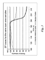
- Figure 3 is a plot of such an output signal for three different experimental arrangements.
- the process being run was a relatively high pressure plasma etch process and the optical emission relating to a particular etch process in the chamber itself; downstream of the turbo pump and with the apparatus shown in Figure 2 .
- the solid line trace starts at a relative intensity of 100% and drops off very much more sharply allowing accurate and quick end point detection and therefore reduces the risk of undered over-etching.
- the sensitivity is importantly better because of clearer, larger signal being generated and so even endpoints, which create relatively small changes in the exhaust gas, can be detected. For example, these may result from small exposed open areas.
- the system can be used even when the main process does not utilise a plasma and the improved response means that the system can be used with shorter etch processes.
- the detector 22 can be any suitable configuration. It could for example be a simple filter in a wide band optical detector, one or more narrow band detectors, such as manual or automatic mono-chromators, a full spectrometer, such as a CCD (Camera Optical Emissions) Spectrometer.
- the window 19 clearly must be transparent to the optical transmission of interest. If the apparatus is very specifically configured, it could even constitute the necessary filter.
- the apparatus not only allows good and quick end point detection. It could be used for other testing processes such as gas quality assessment, leak checking and window clouding measurements.
Landscapes
- Chemical & Material Sciences (AREA)
- Engineering & Computer Science (AREA)
- Physics & Mathematics (AREA)
- Plasma & Fusion (AREA)
- Analytical Chemistry (AREA)
- Metallurgy (AREA)
- Materials Engineering (AREA)
- Mechanical Engineering (AREA)
- Organic Chemistry (AREA)
- General Chemical & Material Sciences (AREA)
- Chemical Kinetics & Catalysis (AREA)
- Spectroscopy & Molecular Physics (AREA)
- Drying Of Semiconductors (AREA)
- Plasma Technology (AREA)
- ing And Chemical Polishing (AREA)
Abstract
Description
- This invention relates to apparatus and methods for chemically etching a workpiece using a process gas.
- It has been known for many decades that when plasma etching a workpiece, it is possible to detect the point at which an etch has cut through a first layer and reached the underlying layer by the change in the optical emission resulting from the change in the exhaust or reaction products being generated and then being ionised by the plasma. Endpoints can also be detected by changes in consumption of etch gas, which can also be detected optically. Initially these emissions were monitored by skilled technicians. Subsequently the process was automated using optical end point detectors.
- Endpoint processes based on the first part approach can only work where there is a plasma being generated and the exhaust and reaction products enter the plasma. There have been, accordingly, a number of proposal, such as that described in
US Patent 4857136 , in which the exhaust products from the turbo pump are ionised and the resultant optical emissions monitored. Experience has shown that arrangements of this sort can have a sluggish response and repeatedly is difficult to achieve due to limitations in local conditions. - From one aspect the invention consists in apparatus for chemically etching a workpiece using a process gas, the apparatus including a chamber for receiving a process gas and having a pumping port for extracting exhaust gases; and a workpiece support located in the chamber upstream of the pumping port characterised in that the chamber further includes a sub-chamber located upstream of the pumping port and downstream of the workpiece support and in that the sub-chamber includes a window and an excitation source, adjacent the window, for creating a plasma in a sample of the exhaust gases to create an optical emission which can be monitored through the window.
- The sub-chamber may include an extension or dead end in which the window is formed and the excitation source may include a coil located around the extension or dead end. The window is preferably close to the pumping port and may, for example, be opposite the pumping port. This enables the window to be adjacent to the exhaust stream.
- The apparatus may further include a detector for monitoring the optical emission visible through the window and may further include a control for determining a process end point from the detected optical emission.
- The apparatus may further include a source for supplying ionised process gas. Additionally or alternatively it may include a plasma source for creating a plasma in the chamber.
- The invention also includes a method of etching using the apparatus defined above wherein the pressure in the chamber during etching is between about 1 to 500 mTor.
- Although the invention has been described above it is to be understood it includes any inventive combination of the features set out above or in the following description.
- The invention may be performed in various ways and a specific embodiment will now be described, by way of example, with reference to the accompanying drawings, in which:
-
Figure 1 is a photograph of part of an etch apparatus; -
Figure 2 is a schematic sectional view through the apparatus ofFigure 1 ; and -
Figure 3 is a graph of the output of a detector showing the traces for different configurations. - An etching apparatus is generally indicated at 10 and has a
chamber 11, in which is located aworkpiece support 12, which is conveniently in the form of a electrostatic chunk, and a source of ionised process gas generally indicated at 13. In a typical prior art arrangement such an apparatus would have a pumping port located at 14, which would be connected to a turbo pump. In the applicants arrangement asub-chamber 15 is attached to theopening 14 and carries apumping port 16 which is connected to aturbo pump 17. - The
sub-chamber 15 is also provided with an extension or dead end 18 that has a window 19 formed in its closed end. Acoil 20 surrounds the extension 18 and is connected to aRF source 21 so that a local plasma can be struck within the extension 18. - A
detector 22 is located outside the window 19 to monitor the optical emissions from the localisedplasma 23 and it feeds it output signals to a control/processor 24, which produces anoutput signal 25 that can be used to control the process within thechamber 11 and may be displayed at 26 if manual control is desired. -
Figure 3 is a plot of such an output signal for three different experimental arrangements. The process being run was a relatively high pressure plasma etch process and the optical emission relating to a particular etch process in the chamber itself; downstream of the turbo pump and with the apparatus shown inFigure 2 . - As can be seen from
Figure 3 there was no detectable change in the signal within the chamber because in the high pressure situation very little reaction product reaches the plasma. (It should be noted that the graph is of relative intensity not actual intensity). - In the foreline (i.e. downstream of the turbo pump) it takes a little while before the relative intensity reaches 100% and then the drop off in intensity is relatively slow and flat. As the intensity initially rises from below 100%, it is quite difficult to set up the equipment to be sure of detecting an end point until the relative intensity has dropped back down again below this starting position. As can be seen from the graph, this in itself could lead to a delay of some 10 seconds before an end point could be established and the relatively small change means that the system is more susceptible to errors and therefore it may not be possible to be certain of determining an end point until up to 20 seconds later, in terms of the process being utilised in the experiment. In contrast the solid line trace starts at a relative intensity of 100% and drops off very much more sharply allowing accurate and quick end point detection and therefore reduces the risk of undered over-etching. The sensitivity is importantly better because of clearer, larger signal being generated and so even endpoints, which create relatively small changes in the exhaust gas, can be detected. For example, these may result from small exposed open areas.
- It will also be appreciated that the system can be used even when the main process does not utilise a plasma and the improved response means that the system can be used with shorter etch processes.
- The
detector 22 can be any suitable configuration. It could for example be a simple filter in a wide band optical detector, one or more narrow band detectors, such as manual or automatic mono-chromators, a full spectrometer, such as a CCD (Camera Optical Emissions) Spectrometer. - The window 19 clearly must be transparent to the optical transmission of interest. If the apparatus is very specifically configured, it could even constitute the necessary filter.
- The apparatus not only allows good and quick end point detection. It could be used for other testing processes such as gas quality assessment, leak checking and window clouding measurements.
Claims (6)
- Apparatus for chemically etching a workpiece using a process gas, the apparatus including a chamber for receiving the process gas and having a pumping port for extracting exhaust gases; and a workpiece support located in the chamber upstream of the pumping port characterised in that the chamber further includes a sub-chamber located upstream of the pumping port and downstream of the workpiece support and in that the sub-chamber includes a window and an excitation source, adjacent the window, for creating a plasma in a sample of the exhaust gases to create an optical emission which can be monitored through the window.
- Apparatus as claimed in claim 1 wherein the sub-chamber includes an extension or dead end in which the window is formed and the excitation source includes a coil or capacitor away located around the extension or dead end.
- Apparatus as claimed in claim 1 or claim 2 wherein the window is generally opposite the pumping port.
- Apparatus as claimed in any one of the preceding claims further including a detector for monitoring the optical emission visible through the window.
- Apparatus as claimed in claim 4 further including a control for determining a process end point from the detected optical emission.
- Apparatus as claimed in any one of the preceding claims further including a source for supplying ionised process gas.
Applications Claiming Priority (1)
| Application Number | Priority Date | Filing Date | Title |
|---|---|---|---|
| GBGB0904240.9A GB0904240D0 (en) | 2009-03-12 | 2009-03-12 | Apparatus for chemically etching a workpiece |
Publications (3)
| Publication Number | Publication Date |
|---|---|
| EP2237309A2 true EP2237309A2 (en) | 2010-10-06 |
| EP2237309A3 EP2237309A3 (en) | 2011-08-03 |
| EP2237309B1 EP2237309B1 (en) | 2019-10-02 |
Family
ID=40600906
Family Applications (1)
| Application Number | Title | Priority Date | Filing Date |
|---|---|---|---|
| EP10154656.2A Active EP2237309B1 (en) | 2009-03-12 | 2010-02-25 | Apparatus for chemically etching a workpiece |
Country Status (7)
| Country | Link |
|---|---|
| US (1) | US9159599B2 (en) |
| EP (1) | EP2237309B1 (en) |
| JP (2) | JP5912011B2 (en) |
| KR (1) | KR101617047B1 (en) |
| CN (1) | CN101840850B (en) |
| GB (1) | GB0904240D0 (en) |
| TW (1) | TWI520210B (en) |
Families Citing this family (3)
| Publication number | Priority date | Publication date | Assignee | Title |
|---|---|---|---|---|
| GB0904240D0 (en) * | 2009-03-12 | 2009-04-22 | Aviza Technology Ltd | Apparatus for chemically etching a workpiece |
| CN102437012A (en) * | 2011-08-04 | 2012-05-02 | 上海华力微电子有限公司 | An Improved Dry Etching Chamber |
| US9691618B2 (en) * | 2015-11-13 | 2017-06-27 | Samsung Electronics Co., Ltd. | Methods of fabricating semiconductor devices including performing an atomic layer etching process |
Citations (1)
| Publication number | Priority date | Publication date | Assignee | Title |
|---|---|---|---|---|
| US4857136A (en) | 1988-06-23 | 1989-08-15 | John Zajac | Reactor monitoring system and method |
Family Cites Families (22)
| Publication number | Priority date | Publication date | Assignee | Title |
|---|---|---|---|---|
| JPH03147318A (en) | 1989-11-01 | 1991-06-24 | Hitachi Ltd | Etching end point determination device |
| US5290383A (en) * | 1991-03-24 | 1994-03-01 | Tokyo Electron Limited | Plasma-process system with improved end-point detecting scheme |
| JP3333657B2 (en) | 1995-02-10 | 2002-10-15 | サイエンステクノロジー株式会社 | Vapor phase etching apparatus and vapor phase etching method |
| JPH09209179A (en) | 1996-01-30 | 1997-08-12 | Nec Corp | Dry etching apparatus and cleaning method thereof |
| JPH11176815A (en) | 1997-12-15 | 1999-07-02 | Ricoh Co Ltd | Dry etching end point determination method and dry etching apparatus |
| US6356741B1 (en) | 1998-09-18 | 2002-03-12 | Allegro Microsystems, Inc. | Magnetic pole insensitive switch circuit |
| US5986747A (en) * | 1998-09-24 | 1999-11-16 | Applied Materials, Inc. | Apparatus and method for endpoint detection in non-ionizing gaseous reactor environments |
| US6366346B1 (en) | 1998-11-19 | 2002-04-02 | Applied Materials, Inc. | Method and apparatus for optical detection of effluent composition |
| US6592817B1 (en) * | 2000-03-31 | 2003-07-15 | Applied Materials, Inc. | Monitoring an effluent from a chamber |
| JP2002057149A (en) * | 2000-08-08 | 2002-02-22 | Tokyo Electron Ltd | Processing apparatus and cleaning method thereof |
| US20020139477A1 (en) * | 2001-03-30 | 2002-10-03 | Lam Research Corporation | Plasma processing method and apparatus with control of plasma excitation power |
| US20030194495A1 (en) * | 2002-04-11 | 2003-10-16 | Applied Materials, Inc. | Crosslink cyclo-siloxane compound with linear bridging group to form ultra low k dielectric |
| US6936551B2 (en) * | 2002-05-08 | 2005-08-30 | Applied Materials Inc. | Methods and apparatus for E-beam treatment used to fabricate integrated circuit devices |
| US7790583B2 (en) | 2004-02-20 | 2010-09-07 | Applied Materials, Inc. | Clean process for an electron beam source |
| FR2887072A1 (en) | 2005-06-08 | 2006-12-15 | Alcatel Sa | IMPROVED SPECTOGRAPHIC SYSTEM WITH PLASMA SOURCE |
| US8092695B2 (en) * | 2006-10-30 | 2012-01-10 | Applied Materials, Inc. | Endpoint detection for photomask etching |
| JP5281766B2 (en) * | 2007-07-31 | 2013-09-04 | ルネサスエレクトロニクス株式会社 | Manufacturing method of semiconductor integrated circuit device |
| US20090104761A1 (en) * | 2007-10-19 | 2009-04-23 | Varian Semiconductor Equipment Associates, Inc. | Plasma Doping System With Charge Control |
| US20100224322A1 (en) * | 2009-03-03 | 2010-09-09 | Applied Materials, Inc. | Endpoint detection for a reactor chamber using a remote plasma chamber |
| GB0904240D0 (en) * | 2009-03-12 | 2009-04-22 | Aviza Technology Ltd | Apparatus for chemically etching a workpiece |
| KR20110103723A (en) * | 2010-03-15 | 2011-09-21 | 삼성전자주식회사 | Process monitoring device and process monitoring method using the same |
| JP5699795B2 (en) * | 2011-05-12 | 2015-04-15 | 富士通セミコンダクター株式会社 | Semiconductor device manufacturing method and semiconductor manufacturing apparatus |
-
2009
- 2009-03-12 GB GBGB0904240.9A patent/GB0904240D0/en not_active Ceased
-
2010
- 2010-02-25 EP EP10154656.2A patent/EP2237309B1/en active Active
- 2010-03-04 TW TW099106273A patent/TWI520210B/en active
- 2010-03-12 CN CN201010176814.2A patent/CN101840850B/en active Active
- 2010-03-12 JP JP2010056423A patent/JP5912011B2/en active Active
- 2010-03-12 KR KR1020100022040A patent/KR101617047B1/en active Active
- 2010-03-12 US US12/722,614 patent/US9159599B2/en active Active
-
2014
- 2014-09-16 JP JP2014188039A patent/JP2015039000A/en active Pending
Patent Citations (1)
| Publication number | Priority date | Publication date | Assignee | Title |
|---|---|---|---|---|
| US4857136A (en) | 1988-06-23 | 1989-08-15 | John Zajac | Reactor monitoring system and method |
Also Published As
| Publication number | Publication date |
|---|---|
| CN101840850A (en) | 2010-09-22 |
| JP2015039000A (en) | 2015-02-26 |
| EP2237309B1 (en) | 2019-10-02 |
| EP2237309A3 (en) | 2011-08-03 |
| US20100230049A1 (en) | 2010-09-16 |
| TWI520210B (en) | 2016-02-01 |
| US9159599B2 (en) | 2015-10-13 |
| GB0904240D0 (en) | 2009-04-22 |
| JP5912011B2 (en) | 2016-04-27 |
| CN101840850B (en) | 2016-08-03 |
| JP2010219534A (en) | 2010-09-30 |
| TW201039387A (en) | 2010-11-01 |
| KR20100103407A (en) | 2010-09-27 |
| KR101617047B1 (en) | 2016-04-29 |
Similar Documents
| Publication | Publication Date | Title |
|---|---|---|
| WO2004104552A3 (en) | Apparatus and method for process monitoring | |
| US7518719B2 (en) | Contaminant analyzer for fuel | |
| WO2003063233A3 (en) | Systems and methods for closed loop defect reduction | |
| WO2005045890A3 (en) | Method and apparatus for etch endpoint detection | |
| US10643830B2 (en) | Specific substance monitoring system using mass spectrometer | |
| WO2007120996A3 (en) | Method and apparatus for compact spectrometer for detecting hazardous agents | |
| US11745229B2 (en) | Endpoint detection of deposition cleaning in a pumping line and a processing chamber | |
| EP1584917A3 (en) | Detection method and detection apparatus of substance in biological sample | |
| JP2006121072A5 (en) | ||
| EP2237309B1 (en) | Apparatus for chemically etching a workpiece | |
| EP2485030A1 (en) | Device for detetcting gas leaks, particualrly for joints of pipes and the like | |
| WO2005068807A3 (en) | Fluid test machine, methods and systems | |
| US20120061589A1 (en) | Method and apparatus for measuring fluorescent material in a liquid | |
| WO2003078899A3 (en) | Method for conducting a cooking process using a cooking process sensor | |
| EP2506007A2 (en) | System for measuring, using a qms, an absolute quantity of each component of a gas | |
| WO2004070455A3 (en) | Optimizing a liquid crystal display (lcd) manufacturing process | |
| CN105206544B (en) | End-point detecting system and its method for monitoring operation states | |
| CN105161395A (en) | Plasma etching apparatus and plasma etching method | |
| CN109655524B (en) | Method for detecting microcracks on riveting surface of dissimilar metal | |
| Eom et al. | Analysis of gas detection sensitivity of a self plasma-optical emission spectrometer using an N2 and Ar gas-mixing evaluation system | |
| JP4860367B2 (en) | Liquid chromatograph | |
| US10088380B2 (en) | Method and system for a sample filter visual contamination check | |
| JP7364377B2 (en) | Explosives inspection equipment | |
| JPH10135196A (en) | Vacuum thin film deposition equipment | |
| WO2005067422A3 (en) | Method and apparatus for inspecting reformer tube |
Legal Events
| Date | Code | Title | Description |
|---|---|---|---|
| PUAI | Public reference made under article 153(3) epc to a published international application that has entered the european phase |
Free format text: ORIGINAL CODE: 0009012 |
|
| AK | Designated contracting states |
Kind code of ref document: A2 Designated state(s): AT BE BG CH CY CZ DE DK EE ES FI FR GB GR HR HU IE IS IT LI LT LU LV MC MK MT NL NO PL PT RO SE SI SK SM TR |
|
| AX | Request for extension of the european patent |
Extension state: AL BA RS |
|
| PUAL | Search report despatched |
Free format text: ORIGINAL CODE: 0009013 |
|
| AK | Designated contracting states |
Kind code of ref document: A3 Designated state(s): AT BE BG CH CY CZ DE DK EE ES FI FR GB GR HR HU IE IS IT LI LT LU LV MC MK MT NL NO PL PT RO SE SI SK SM TR |
|
| AX | Request for extension of the european patent |
Extension state: AL BA RS |
|
| RIC1 | Information provided on ipc code assigned before grant |
Ipc: H01L 21/00 20060101AFI20110630BHEP |
|
| 17P | Request for examination filed |
Effective date: 20120124 |
|
| 111Z | Information provided on other rights and legal means of execution |
Free format text: AT BE BG CH CY CZ DE DK EE ES FI FR GB GR HR HU IE IS IT LT LU LV MC MK MT NL NO PL PT RO SE SI SK SM TR Effective date: 20150702 |
|
| D11X | Information provided on other rights and legal means of execution (deleted) | ||
| STAA | Information on the status of an ep patent application or granted ep patent |
Free format text: STATUS: EXAMINATION IS IN PROGRESS |
|
| 17Q | First examination report despatched |
Effective date: 20180919 |
|
| REG | Reference to a national code |
Ref country code: DE Ref legal event code: R079 Ref document number: 602010061284 Country of ref document: DE Free format text: PREVIOUS MAIN CLASS: H01L0021000000 Ipc: H01J0037320000 |
|
| GRAP | Despatch of communication of intention to grant a patent |
Free format text: ORIGINAL CODE: EPIDOSNIGR1 |
|
| STAA | Information on the status of an ep patent application or granted ep patent |
Free format text: STATUS: GRANT OF PATENT IS INTENDED |
|
| RIC1 | Information provided on ipc code assigned before grant |
Ipc: H01L 21/67 20060101ALI20190404BHEP Ipc: H01J 37/32 20060101AFI20190404BHEP |
|
| INTG | Intention to grant announced |
Effective date: 20190426 |
|
| GRAS | Grant fee paid |
Free format text: ORIGINAL CODE: EPIDOSNIGR3 |
|
| GRAA | (expected) grant |
Free format text: ORIGINAL CODE: 0009210 |
|
| STAA | Information on the status of an ep patent application or granted ep patent |
Free format text: STATUS: THE PATENT HAS BEEN GRANTED |
|
| AK | Designated contracting states |
Kind code of ref document: B1 Designated state(s): AT BE BG CH CY CZ DE DK EE ES FI FR GB GR HR HU IE IS IT LI LT LU LV MC MK MT NL NO PL PT RO SE SI SK SM TR |
|
| REG | Reference to a national code |
Ref country code: GB Ref legal event code: FG4D |
|
| REG | Reference to a national code |
Ref country code: CH Ref legal event code: EP Ref country code: AT Ref legal event code: REF Ref document number: 1187101 Country of ref document: AT Kind code of ref document: T Effective date: 20191015 |
|
| REG | Reference to a national code |
Ref country code: DE Ref legal event code: R096 Ref document number: 602010061284 Country of ref document: DE |
|
| REG | Reference to a national code |
Ref country code: IE Ref legal event code: FG4D |
|
| REG | Reference to a national code |
Ref country code: NL Ref legal event code: MP Effective date: 20191002 |
|
| REG | Reference to a national code |
Ref country code: LT Ref legal event code: MG4D |
|
| REG | Reference to a national code |
Ref country code: AT Ref legal event code: MK05 Ref document number: 1187101 Country of ref document: AT Kind code of ref document: T Effective date: 20191002 |
|
| PG25 | Lapsed in a contracting state [announced via postgrant information from national office to epo] |
Ref country code: ES Free format text: LAPSE BECAUSE OF FAILURE TO SUBMIT A TRANSLATION OF THE DESCRIPTION OR TO PAY THE FEE WITHIN THE PRESCRIBED TIME-LIMIT Effective date: 20191002 Ref country code: NL Free format text: LAPSE BECAUSE OF FAILURE TO SUBMIT A TRANSLATION OF THE DESCRIPTION OR TO PAY THE FEE WITHIN THE PRESCRIBED TIME-LIMIT Effective date: 20191002 Ref country code: LV Free format text: LAPSE BECAUSE OF FAILURE TO SUBMIT A TRANSLATION OF THE DESCRIPTION OR TO PAY THE FEE WITHIN THE PRESCRIBED TIME-LIMIT Effective date: 20191002 Ref country code: SE Free format text: LAPSE BECAUSE OF FAILURE TO SUBMIT A TRANSLATION OF THE DESCRIPTION OR TO PAY THE FEE WITHIN THE PRESCRIBED TIME-LIMIT Effective date: 20191002 Ref country code: PL Free format text: LAPSE BECAUSE OF FAILURE TO SUBMIT A TRANSLATION OF THE DESCRIPTION OR TO PAY THE FEE WITHIN THE PRESCRIBED TIME-LIMIT Effective date: 20191002 Ref country code: LT Free format text: LAPSE BECAUSE OF FAILURE TO SUBMIT A TRANSLATION OF THE DESCRIPTION OR TO PAY THE FEE WITHIN THE PRESCRIBED TIME-LIMIT Effective date: 20191002 Ref country code: NO Free format text: LAPSE BECAUSE OF FAILURE TO SUBMIT A TRANSLATION OF THE DESCRIPTION OR TO PAY THE FEE WITHIN THE PRESCRIBED TIME-LIMIT Effective date: 20200102 Ref country code: GR Free format text: LAPSE BECAUSE OF FAILURE TO SUBMIT A TRANSLATION OF THE DESCRIPTION OR TO PAY THE FEE WITHIN THE PRESCRIBED TIME-LIMIT Effective date: 20200103 Ref country code: PT Free format text: LAPSE BECAUSE OF FAILURE TO SUBMIT A TRANSLATION OF THE DESCRIPTION OR TO PAY THE FEE WITHIN THE PRESCRIBED TIME-LIMIT Effective date: 20200203 Ref country code: BG Free format text: LAPSE BECAUSE OF FAILURE TO SUBMIT A TRANSLATION OF THE DESCRIPTION OR TO PAY THE FEE WITHIN THE PRESCRIBED TIME-LIMIT Effective date: 20200102 Ref country code: FI Free format text: LAPSE BECAUSE OF FAILURE TO SUBMIT A TRANSLATION OF THE DESCRIPTION OR TO PAY THE FEE WITHIN THE PRESCRIBED TIME-LIMIT Effective date: 20191002 Ref country code: AT Free format text: LAPSE BECAUSE OF FAILURE TO SUBMIT A TRANSLATION OF THE DESCRIPTION OR TO PAY THE FEE WITHIN THE PRESCRIBED TIME-LIMIT Effective date: 20191002 |
|
| PG25 | Lapsed in a contracting state [announced via postgrant information from national office to epo] |
Ref country code: IS Free format text: LAPSE BECAUSE OF FAILURE TO SUBMIT A TRANSLATION OF THE DESCRIPTION OR TO PAY THE FEE WITHIN THE PRESCRIBED TIME-LIMIT Effective date: 20200224 Ref country code: CZ Free format text: LAPSE BECAUSE OF FAILURE TO SUBMIT A TRANSLATION OF THE DESCRIPTION OR TO PAY THE FEE WITHIN THE PRESCRIBED TIME-LIMIT Effective date: 20191002 Ref country code: HR Free format text: LAPSE BECAUSE OF FAILURE TO SUBMIT A TRANSLATION OF THE DESCRIPTION OR TO PAY THE FEE WITHIN THE PRESCRIBED TIME-LIMIT Effective date: 20191002 |
|
| REG | Reference to a national code |
Ref country code: DE Ref legal event code: R097 Ref document number: 602010061284 Country of ref document: DE |
|
| PG2D | Information on lapse in contracting state deleted |
Ref country code: IS |
|
| PG25 | Lapsed in a contracting state [announced via postgrant information from national office to epo] |
Ref country code: RO Free format text: LAPSE BECAUSE OF FAILURE TO SUBMIT A TRANSLATION OF THE DESCRIPTION OR TO PAY THE FEE WITHIN THE PRESCRIBED TIME-LIMIT Effective date: 20191002 Ref country code: DK Free format text: LAPSE BECAUSE OF FAILURE TO SUBMIT A TRANSLATION OF THE DESCRIPTION OR TO PAY THE FEE WITHIN THE PRESCRIBED TIME-LIMIT Effective date: 20191002 Ref country code: EE Free format text: LAPSE BECAUSE OF FAILURE TO SUBMIT A TRANSLATION OF THE DESCRIPTION OR TO PAY THE FEE WITHIN THE PRESCRIBED TIME-LIMIT Effective date: 20191002 Ref country code: IS Free format text: LAPSE BECAUSE OF FAILURE TO SUBMIT A TRANSLATION OF THE DESCRIPTION OR TO PAY THE FEE WITHIN THE PRESCRIBED TIME-LIMIT Effective date: 20200202 |
|
| PLBE | No opposition filed within time limit |
Free format text: ORIGINAL CODE: 0009261 |
|
| STAA | Information on the status of an ep patent application or granted ep patent |
Free format text: STATUS: NO OPPOSITION FILED WITHIN TIME LIMIT |
|
| PG25 | Lapsed in a contracting state [announced via postgrant information from national office to epo] |
Ref country code: SK Free format text: LAPSE BECAUSE OF FAILURE TO SUBMIT A TRANSLATION OF THE DESCRIPTION OR TO PAY THE FEE WITHIN THE PRESCRIBED TIME-LIMIT Effective date: 20191002 Ref country code: IT Free format text: LAPSE BECAUSE OF FAILURE TO SUBMIT A TRANSLATION OF THE DESCRIPTION OR TO PAY THE FEE WITHIN THE PRESCRIBED TIME-LIMIT Effective date: 20191002 Ref country code: SM Free format text: LAPSE BECAUSE OF FAILURE TO SUBMIT A TRANSLATION OF THE DESCRIPTION OR TO PAY THE FEE WITHIN THE PRESCRIBED TIME-LIMIT Effective date: 20191002 |
|
| 26N | No opposition filed |
Effective date: 20200703 |
|
| REG | Reference to a national code |
Ref country code: CH Ref legal event code: PL |
|
| REG | Reference to a national code |
Ref country code: BE Ref legal event code: MM Effective date: 20200229 |
|
| PG25 | Lapsed in a contracting state [announced via postgrant information from national office to epo] |
Ref country code: MC Free format text: LAPSE BECAUSE OF FAILURE TO SUBMIT A TRANSLATION OF THE DESCRIPTION OR TO PAY THE FEE WITHIN THE PRESCRIBED TIME-LIMIT Effective date: 20191002 Ref country code: LU Free format text: LAPSE BECAUSE OF NON-PAYMENT OF DUE FEES Effective date: 20200225 |
|
| PG25 | Lapsed in a contracting state [announced via postgrant information from national office to epo] |
Ref country code: SI Free format text: LAPSE BECAUSE OF FAILURE TO SUBMIT A TRANSLATION OF THE DESCRIPTION OR TO PAY THE FEE WITHIN THE PRESCRIBED TIME-LIMIT Effective date: 20191002 Ref country code: LI Free format text: LAPSE BECAUSE OF NON-PAYMENT OF DUE FEES Effective date: 20200229 Ref country code: CH Free format text: LAPSE BECAUSE OF NON-PAYMENT OF DUE FEES Effective date: 20200229 |
|
| PG25 | Lapsed in a contracting state [announced via postgrant information from national office to epo] |
Ref country code: IE Free format text: LAPSE BECAUSE OF NON-PAYMENT OF DUE FEES Effective date: 20200225 |
|
| PG25 | Lapsed in a contracting state [announced via postgrant information from national office to epo] |
Ref country code: BE Free format text: LAPSE BECAUSE OF NON-PAYMENT OF DUE FEES Effective date: 20200229 |
|
| PG25 | Lapsed in a contracting state [announced via postgrant information from national office to epo] |
Ref country code: TR Free format text: LAPSE BECAUSE OF FAILURE TO SUBMIT A TRANSLATION OF THE DESCRIPTION OR TO PAY THE FEE WITHIN THE PRESCRIBED TIME-LIMIT Effective date: 20191002 Ref country code: MT Free format text: LAPSE BECAUSE OF FAILURE TO SUBMIT A TRANSLATION OF THE DESCRIPTION OR TO PAY THE FEE WITHIN THE PRESCRIBED TIME-LIMIT Effective date: 20191002 Ref country code: CY Free format text: LAPSE BECAUSE OF FAILURE TO SUBMIT A TRANSLATION OF THE DESCRIPTION OR TO PAY THE FEE WITHIN THE PRESCRIBED TIME-LIMIT Effective date: 20191002 |
|
| PG25 | Lapsed in a contracting state [announced via postgrant information from national office to epo] |
Ref country code: MK Free format text: LAPSE BECAUSE OF FAILURE TO SUBMIT A TRANSLATION OF THE DESCRIPTION OR TO PAY THE FEE WITHIN THE PRESCRIBED TIME-LIMIT Effective date: 20191002 |
|
| P01 | Opt-out of the competence of the unified patent court (upc) registered |
Effective date: 20230525 |
|
| REG | Reference to a national code |
Ref country code: DE Ref legal event code: R082 Ref document number: 602010061284 Country of ref document: DE Representative=s name: KANDLBINDER, MARKUS, DIPL.-PHYS., DE |
|
| PGFP | Annual fee paid to national office [announced via postgrant information from national office to epo] |
Ref country code: GB Payment date: 20260227 Year of fee payment: 17 |
|
| PGFP | Annual fee paid to national office [announced via postgrant information from national office to epo] |
Ref country code: DE Payment date: 20260227 Year of fee payment: 17 |
|
| PGFP | Annual fee paid to national office [announced via postgrant information from national office to epo] |
Ref country code: FR Payment date: 20260225 Year of fee payment: 17 |