EP2237159A1 - Analog-to-digital converter device with Direct Memory Access - Google Patents
Analog-to-digital converter device with Direct Memory Access Download PDFInfo
- Publication number
- EP2237159A1 EP2237159A1 EP10157430A EP10157430A EP2237159A1 EP 2237159 A1 EP2237159 A1 EP 2237159A1 EP 10157430 A EP10157430 A EP 10157430A EP 10157430 A EP10157430 A EP 10157430A EP 2237159 A1 EP2237159 A1 EP 2237159A1
- Authority
- EP
- European Patent Office
- Prior art keywords
- group
- conversion
- channels
- adc
- analog
- Prior art date
- Legal status (The legal status is an assumption and is not a legal conclusion. Google has not performed a legal analysis and makes no representation as to the accuracy of the status listed.)
- Granted
Links
Images

Classifications
-
- G—PHYSICS
- G06—COMPUTING OR CALCULATING; COUNTING
- G06F—ELECTRIC DIGITAL DATA PROCESSING
- G06F13/00—Interconnection of, or transfer of information or other signals between, memories, input/output devices or central processing units
- G06F13/14—Handling requests for interconnection or transfer
- G06F13/20—Handling requests for interconnection or transfer for access to input/output bus
- G06F13/28—Handling requests for interconnection or transfer for access to input/output bus using burst mode transfer, e.g. direct memory access DMA, cycle steal
Definitions
- the disclosure refers to analog-digital converters.
- the disclosure was devised with particular attention paid to its possible use in high speed analog-digital converters.
- ADC analog-digital converters
- DMA Direct Memory Access
- the object of the invention is providing an analog-digital converter capable of overcoming such drawbacks.
- the analog-digital converter supports an operating method wherein the DMA access may be disabled and the results of the conversion are saved only in local registers, such as for example data registers normally used for temporarily saving instantaneous measurements. This also allows an efficient use of the data registers and the maintenance of the entire bandwidth of the bus, in particular when configured to perform continuous conversions.
- each conversion channel is assigned to at least one group of channels.
- the conversion results of one first group, identified as a regular group are temporarily saved in a single local register and they are subsequently transferred to a memory, for example a microprocessor RAM memory, through a DMA access.
- a memory for example a microprocessor RAM memory
- each conversion result of a second group, identified as an injected group is saved in a respective register.
- associated to the ADC is a plurality of configuration registers for defining at least two groups of channels: regular and injected.
- the results of the conversion of the regular group are temporarily saved in a single local register and subsequently transferred to a memory through a DMA access, while the result of each conversion of the injected group is saved in a respective data register.
- ADC RSQR and ADC_JSQR are used to respectively specify the group of regular and injected channels.
- the ADC_JSQR register is a register that comprises at least (5 ⁇ 4) + 2 bits.
- the ADC_JSQR register allows specifying a 4-channel arbitrary sequence (each for example encoded in a binary form with 5 bits) among the 19 channels available.
- the 2 remaining bits (for example the most significant bits) of the ADC_JSQR register are used to define the number of channels to be converted. This means that the ADC is capable of converting up to 4 channels for the injected group and thus there are also 4 data registers for the results of the channel conversions of the injected group.
- the ADC_RSQR register is a register that comprises at least (5 ⁇ 16) + 4 bits for specifying a 16-channel arbitrary sequence among the 19 channels available.
- the remaining 4 bits (ad for example the most significant bits) of the ADC_RQR register are used to define the number of channels to be converted. This means that the ADC is capable of converting up to 16 channels for the regular group, wherein the results of the channel conversions of the regular group are saved only temporarily in a single data register before being transferred to a memory through a DMA access.
- a reserved channel number (for example the "00000” or "11111” bit sequence) is used for specifying the number of channels unused in the channel sequence.
- the ADC is associated to a microprocessor and the configuration registers are accessible through respective registers.
- the configuration register is divided into several "virtual" configuration registers each accessible through a respective address. In this manner, the microprocessor or a program executed thereby may directly access (i.e. read or encode) the content of the configuration registers.
- Figure 1 shows an example of the mapping for the 22 bits of the ADC_JSQR register accessible through the "0x38h" address.
- an identifier JL (bit [21:20]) defines the number of channels for the injected group and the identifiers JSQ_CO...JSQ_C3 (bit [19: 0]) define the channel sequence for the injected group.
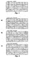
- Figures 2a, 2b and 2c show a mapping example for the 84 bits of the ADC_RSQR register.
- ADC_RSQR1, ADC_RSQR2 and ADC_RSQR3 are used, wherein said three virtual registers are attained respectively through addresses "0x2Ch”, "0x30h” and "0x34h”.
- an RL identifier i.e. the bits [23:20] of the ADC_RSQR1 register
- Identifiers RSQ_CO...RSQ_C15 i.e. bits [19:0] of the ADC_RSQR1 register, bits [29:0] of the ADC_RSQR2 register and bits [29:0] of the ADC_RSQR3 register
- the conversion of the channels in the injected group usually starts after a triggering event, for example an external trigger, and the conversion may send an interrupt towards the conversion of the sequence of channels in the regular group.
- a triggering event for example an external trigger
- the ADC also supports a mode of operation wherein the conversion of the channels in the injected group is activated automatically when the conversion of the channels in the regular group terminates, thus avoiding requiring a special external triggering event. For example, this allows converting all the 19 channels of the converter with a single triggering event by suitably setting the ADC-RSQR and ADC_JSQR configuration registers.
- Figure 3 is a block diagram of a possible embodiment of such converter 10 which supports the automatic activation of the channel conversion in the injected group.
- the conversion of the regular group is activated through a setting of a bit in a configuration register.
- this bit may be set upon request (for example by a microprocessor) or by means of an external trigger.
- the conversion of the groups of channels is controlled through a control module, for example a Finite-State Machine (FSM) 100 provided in the converter 10 by means of a digital circuit.
- FSM Finite-State Machine
- the FSM 100 actuates a multiplexer 102 to select the regular group and the entire sequence of channels in the regular group, as defined in the ADC_RSQR register, is loaded into a buffer 104.
- the FSM 100 actuates a second multiplexer 106 through a channel selector S, in such a manner to select the first element in the buffer 104 (i.e. the first normal channel).
- the multiplexer 106 provides the number of the channel currently selected C encoded in binary form with 5 bits.
- the FSM 100 activates the conversion by means of an activation signal ADC_SOC sent to a conversion module 108.
- the conversion module 108 converts the channel currently selected C and generates a signal ADC_EOC at the end of the conversion.
- the FSM 100 receives the ADC_EOC signal and, if other channels in the regular group need to be converted, increases the channel selector S to select the next channel of the regular group through the multiplexer 106.
- the FSM 100 increases the channel selector S until value RL (i.e. bits [23:20] of the ADC_RSQR1 register) is reached, i.e. the length of the sequence of the regular group.
- the signal of the channels C would first provide value "0x2h” and then value "0x7h".
- the FSM 100 selects - through the multiplexer 102 - the ADC_JSQR register and the entire sequence of channels in the injected group, as defined in the ADC_JSQR register, is loaded into the buffer 104.
- the FSM 100 actuates the multiplexer 106 to select the channels in the buffer 104 and the respective channels of the injected group are converted by the ADC until the JL value (i.e. the bits [21:20] of the ADC_JSQR register) is attained, i.e. the length of the sequence of the injected group.
- the buffer 104 comprises 16 positions with 5 bits, thus allowing storing the sequence of the regular group or the sequence of the injected group.
- a larger buffer could be used, for example a buffer with 20 positions, in such a manner to directly store both the sequence of the regular group the sequence of the injected group.
- the use of the buffer 104 allows the user to change the value of the ADC_RSQR and ADC_JSQR registers during conversion; these values are loaded into the buffer 104 only when the current conversion ends.
- the use of the buffer 104 may also allow minimising the combining path towards the conversion module 108.
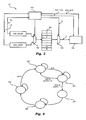
- Figure 4 shows a state diagram of an embodiment of the FSM 100.
- the FSM is initialised (for example by means of a reset) in an initial state 200.
- the FSM passes from the initial state 200 to a state 202, in which the conversion of the channels of the regular group is activated.
- the sequence of the normal channels is saved in the buffer 104 and the conversion of the first normal channel is activated, for example by activating the start of conversion signal ADC_SOC.
- the conversion module 108 receives the ADC_SOC signal, converts the channel currently selected C and activates an end of conversion signal ADC_EOC at the end of each conversion.
- the ADC_EOC signal allows the FSM to increase the channel selector S for the multiplexer 106 in such a manner to indicate the subsequent position in the buffer 104.
- the channel currently selected C acquires the value of the next channel and a new conversion is started, for example by activating the start of conversion signal ADC_SOC again.
- an end of conversion signal EOC of the is generated (and preferably saved in a configuration register).
- the FSM evolves towards a state 204 in which the injected group is selected, through the multiplexer 102.
- the sequence of injected channels is saved in the buffer 104 and the FSM evolves towards a state 206.
- the FSM returns to the initial state 200.
- state 206 the conversion of the channels in the injected group is carried out (this occurs in a manner substantially similar to the conversion of the regular group) until the length of the sequence of the injected group (i.e. the bits [21:20] of the ADC_JSQR register)is attained.
- the FSM After activating the conversion of the last channel of the injected group, the FSM evolves towards a standby state 208 awaiting for the arrival of the end of conversion signal ADC_EOC regarding the conversion of the last channel of the injected group. Lastly an end of conversion signal of the channels of the injected group JEOC is generated (and preferably saved in a configuration register); the FSM returns to the initial state 200.
- Figure 5 shows an application example wherein the previously described analog-digital converter may be applied.
- figure 5 shows an embodiment of a System-on-Chip (SoC) containing two converters - ADC1 and ADC2 - with each converter having the architecture illustrated in figure 3 , and a synchronization module 12, which receives a trigger signal TR.
- SoC System-on-Chip
- such systems may be used in a motor drive scheme such to require the detection of electrical currents: for example in the case of field oriented control or three-phase brushless motor control.
- the two ADC converters are synchronised in such a manner to gather simultaneous samples of two independent signals, such as, for example, two of the three currents in the three-phase motor windings.
- Some systems may also measure all the three three-phase motor currents through a single shunt resistor, reducing the cost of the system.
- an analog signal may be measured twice at very precise moments, synchronised for example with a PWM generator.
- a synchronization mechanism may be provided to trigger at least two conversions without limitation on any temporary interval with a single trigger signal TR.
- the synchronization module 12 receives an external trigger TR as input. Subsequently, the module 12 alternatively activates the conversion of one of the two converters ADC1 and ADC2.
- the described ADC allows:
- too frequent trigger signals may cause the loss of one of the alternating conversions.
- the module 12 may receive the external trigger TR as input and the information regarding the occupation and/or availability of each ADC, for example by means of a state signal.
- the module 12 receives an availability signal ADC1_idle for converter ADC1 (for example having the logic level '1' no conversion is carried out) and an availability signal ADC2_idle for converter ADC2.
- an availability signal ADC1_idle for converter ADC1 for example having the logic level '1' no conversion is carried out
- such signal may be generated by means of the previous ADC_EOC signals (for each single conversion), EOC (for the regular group) or JEOC (for the injected group).
- the module 12 thus generates the respective start of conversion signals SOC for converters ADC1 and ADC2.
- Figure 6 shows an example of a possible external trigger TR sequence and a respective (desirable) alternating activation of converters ADC1 and ADC2.
- Figure 6 shows a sequence of 10 trigger events (called “1st Trig”, “2nd Trig”, “3rd Trig”, “4th Trig” ... “10th Trig”), which activate the conversion of converters ADC1 and ADC2, including data acquisition (called “sampling") and data conversion (called “conversion”).
- conversion is carried out by means of a channel of the injected group and thus, after each conversion, an end of conversion signal JEOC is generated.
- an external trigger TR event is not considered if both the ADCs are already carrying out a conversion.
- the trigger TR event is lost and the subsequent trigger event always activates the conversion of the first converter ADC1.
- the "3rd Trig" and "8th Trig" signals do not cause an activation of one of the two converted ones, in that both converters are already performing conversions.
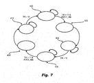
- Figure 7 is a state diagram of a possible embodiment of the synchronisation module 12.
- state 402 the conversion of the first converter ADC1 (for example through a pulse with level logic '1' for 1 clock cycle) is activated and the module 12 evolves towards the subsequent state 404.
- state 408 the conversion of the second converter ADC2 is activated and the module 12 evolves towards the next state 410.
Landscapes
- Engineering & Computer Science (AREA)
- Theoretical Computer Science (AREA)
- Physics & Mathematics (AREA)
- General Engineering & Computer Science (AREA)
- General Physics & Mathematics (AREA)
- Analogue/Digital Conversion (AREA)
Abstract
- a first configuration register (ADC_RSQR) for configuring a first group of channels, wherein the conversion result of the channels of the first group is transferred to a memory via a direct memory access, and
- a second configuration register (ADC_JSQR) for configuring a second group of channels, wherein each channel of said second group of channels has associated a respective data register, and wherein the conversion results of the channels of the second group are stored in the respective data registers.
Description
- The disclosure refers to analog-digital converters.
- The disclosure was devised with particular attention paid to its possible use in high speed analog-digital converters.
- Known in the prior art are various solutions for analog-digital converters (ADC) which transmit conversion results directly into a memory, for example of a microprocessor, through Direct Memory Access (DMA). Such converters allow optimising the use of the silicon area, given that one single data register, for example on 12 bits, is required to temporarily save the results of the conversion before transferring the same to the memory.
- The inventors observed that these DMA transfers may slow and even stop the operation of the CPU and they may thus reduce the performance of the system. For example, this behaviour is particularly disadvantageous if a continuous-conversion high-speed ADC converter is used, for example for monitoring slow changing variables.
- Thus the object of the invention is providing an analog-digital converter capable of overcoming such drawbacks.
- According to the invention, such object is achieved by means of a device having the characteristics referred to in the claims that follow. The invention also regards a corresponding system as well as a corresponding method.
- The claims form an integral part of the technical disclosure provided herein in relation to the invention.
- In an embodiment, the analog-digital converter supports an operating method wherein the DMA access may be disabled and the results of the conversion are saved only in local registers, such as for example data registers normally used for temporarily saving instantaneous measurements. This also allows an efficient use of the data registers and the maintenance of the entire bandwidth of the bus, in particular when configured to perform continuous conversions.
- In an embodiment, each conversion channel is assigned to at least one group of channels.
- In an embodiment, the conversion results of one first group, identified as a regular group, are temporarily saved in a single local register and they are subsequently transferred to a memory, for example a microprocessor RAM memory, through a DMA access.
- In an embodiment, each conversion result of a second group, identified as an injected group, is saved in a respective register.
- The invention will now be described, purely for exemplary and non-limiting purposes, with reference to the attached representations, wherein:
-
Figures 1, 2a, 2b and 2c show an embodiment of the configuration registers of an ADC, -
Figure 3 is a block diagram of a possible embodiment of an ADC, -
Figure 4 is a state diagram of a possible control scheme of the ADC offigure 3 , and -
Figures 5 - 7 show an example of an application of the ADC ofFigure 3 . - Illustrated in the following description are various specific details aimed at an in-depth understanding of the embodiments. The embodiments may be obtained without one or more specific details, or through other methods, components, materials etc. In other cases, known structures, materials or operations are not shown or described in detail to avoid obscuring the various aspects of the embodiments.
- Reference to "an embodiment" in this description indicates that a particular configuration, structure or characteristic described regarding the embodiment is included in at least one embodiment. Hence, expressions such as "in an embodiment", possibly present in various parts of this description do not necessarily refer to the same embodiment. Furthermore, particular configurations, structures or characteristics may be combined in any suitable manner in one or more embodiments.
- References herein are used for facilitating the reader and thus they do not define the scope of protection or the range of the embodiments.
- Considered in the following description, purely for exemplification purposes, is a 19-channel ADC.
- In the embodiment considered, associated to the ADC is a plurality of configuration registers for defining at least two groups of channels: regular and injected.
- The results of the conversion of the regular group are temporarily saved in a single local register and subsequently transferred to a memory through a DMA access, while the result of each conversion of the injected group is saved in a respective data register.
- In the embodiment considered, two registers, ADC RSQR and ADC_JSQR, are used to respectively specify the group of regular and injected channels.
- In an embodiment, the ADC_JSQR register is a register that comprises at least (5 × 4) + 2 bits. In particular, the ADC_JSQR register allows specifying a 4-channel arbitrary sequence (each for example encoded in a binary form with 5 bits) among the 19 channels available. The 2 remaining bits (for example the most significant bits) of the ADC_JSQR register are used to define the number of channels to be converted. This means that the ADC is capable of converting up to 4 channels for the injected group and thus there are also 4 data registers for the results of the channel conversions of the injected group.
- In an embodiment, the ADC_RSQR register is a register that comprises at least (5 × 16) + 4 bits for specifying a 16-channel arbitrary sequence among the 19 channels available. In an analogous manner, the remaining 4 bits (ad for example the most significant bits) of the ADC_RQR register are used to define the number of channels to be converted. This means that the ADC is capable of converting up to 16 channels for the regular group, wherein the results of the channel conversions of the regular group are saved only temporarily in a single data register before being transferred to a memory through a DMA access.
- In an embodiment, instead of using the number of dedicated bits for specifying the number of channels to be converted, a reserved channel number (for example the "00000" or "11111" bit sequence) is used for specifying the number of channels unused in the channel sequence.
- In an embodiment, the ADC is associated to a microprocessor and the configuration registers are accessible through respective registers. In particular, if the length of a configuration register exceeds the width of the bus (for example 32 bits), the configuration register is divided into several "virtual" configuration registers each accessible through a respective address. In this manner, the microprocessor or a program executed thereby may directly access (i.e. read or encode) the content of the configuration registers.
-
Figure 1 shows an example of the mapping for the 22 bits of the ADC_JSQR register accessible through the "0x38h" address. In particular, an identifier JL (bit [21:20]) defines the number of channels for the injected group and the identifiers JSQ_CO...JSQ_C3 (bit [19: 0]) define the channel sequence for the injected group. - For example, if the 22 bits of the ADC_JSQR register have the following content:
- ADC_JSQR(21:0) = 10 00011 00011 00111 00010
- the ADC converts three channels for the injected group (i.e. the "10" bits sequence sets the length of the sequence to three) and the converted channels are
channels -
Figures 2a, 2b and 2c show a mapping example for the 84 bits of the ADC_RSQR register. In particular, three 32-bit virtual registers named ADC_RSQR1, ADC_RSQR2 and ADC_RSQR3 are used, wherein said three virtual registers are attained respectively through addresses "0x2Ch", "0x30h" and "0x34h". - In the embodiment considered, in order to specify the number of channels to be converted for the regular group an RL identifier (i.e. the bits [23:20] of the ADC_RSQR1 register)is used. Identifiers RSQ_CO...RSQ_C15 (i.e. bits [19:0] of the ADC_RSQR1 register, bits [29:0] of the ADC_RSQR2 register and bits [29:0] of the ADC_RSQR3 register) define the sequence of the channels of the regular group.
- For example, if the 84 bits of the ADC_RSQR register have the following contents:
- ADC_RSQR(83:0) = 0001 ... 00011 00011 00111 00010
- the ADC converts two channels (i.e. the sequence of "0001" bits sets the length of the sequence to two) and the converted channels are
channels 2 and 7. - The conversion of the channels in the injected group usually starts after a triggering event, for example an external trigger, and the conversion may send an interrupt towards the conversion of the sequence of channels in the regular group.
- In an embodiment, the ADC also supports a mode of operation wherein the conversion of the channels in the injected group is activated automatically when the conversion of the channels in the regular group terminates, thus avoiding requiring a special external triggering event. For example, this allows converting all the 19 channels of the converter with a single triggering event by suitably setting the ADC-RSQR and ADC_JSQR configuration registers.
-
Figure 3 is a block diagram of a possible embodiment ofsuch converter 10 which supports the automatic activation of the channel conversion in the injected group. - In the embodiment considered, the conversion of the regular group is activated through a setting of a bit in a configuration register. For example, this bit may be set upon request (for example by a microprocessor) or by means of an external trigger.
- At the end of the conversion of the channels in the regular group, if a respective bit in a configuration register indicates that the automatic conversion is activated (for example when the JAUTO bit is set to '1'), the conversion of the channels in the injected group is activated.
- In the embodiment considered, the conversion of the groups of channels is controlled through a control module, for example a Finite-State Machine (FSM) 100 provided in the
converter 10 by means of a digital circuit. - At the beginning, the
FSM 100 actuates amultiplexer 102 to select the regular group and the entire sequence of channels in the regular group, as defined in the ADC_RSQR register, is loaded into abuffer 104. - The
FSM 100 actuates asecond multiplexer 106 through a channel selector S, in such a manner to select the first element in the buffer 104 (i.e. the first normal channel). For example, in the embodiment considered, themultiplexer 106 provides the number of the channel currently selected C encoded in binary form with 5 bits. - Subsequently, the
FSM 100 activates the conversion by means of an activation signal ADC_SOC sent to aconversion module 108. Theconversion module 108 converts the channel currently selected C and generates a signal ADC_EOC at the end of the conversion. - The
FSM 100 receives the ADC_EOC signal and, if other channels in the regular group need to be converted, increases the channel selector S to select the next channel of the regular group through themultiplexer 106. TheFSM 100 increases the channel selector S until value RL (i.e. bits [23:20] of the ADC_RSQR1 register) is reached, i.e. the length of the sequence of the regular group. - For example, for the previous exemplifying sequence regarding the ADC_RSQR register, the signal of the channels C would first provide value "0x2h" and then value "0x7h".
- Subsequently, the
FSM 100 selects - through the multiplexer 102 - the ADC_JSQR register and the entire sequence of channels in the injected group, as defined in the ADC_JSQR register, is loaded into thebuffer 104. In a manner substantially similar to the case of the regular group, theFSM 100 actuates themultiplexer 106 to select the channels in thebuffer 104 and the respective channels of the injected group are converted by the ADC until the JL value (i.e. the bits [21:20] of the ADC_JSQR register) is attained, i.e. the length of the sequence of the injected group. - In the embodiment considered, the
buffer 104 comprises 16 positions with 5 bits, thus allowing storing the sequence of the regular group or the sequence of the injected group. However, even a larger buffer could be used, for example a buffer with 20 positions, in such a manner to directly store both the sequence of the regular group the sequence of the injected group. - For example, the use of the
buffer 104 allows the user to change the value of the ADC_RSQR and ADC_JSQR registers during conversion; these values are loaded into thebuffer 104 only when the current conversion ends. The use of thebuffer 104 may also allow minimising the combining path towards theconversion module 108. -
Figure 4 shows a state diagram of an embodiment of theFSM 100. - The FSM is initialised (for example by means of a reset) in an
initial state 200. When the conversion of the channels is activated (for example through a start of conversion signal SOC), the FSM passes from theinitial state 200 to astate 202, in which the conversion of the channels of the regular group is activated. In particular, incondition 202, the sequence of the normal channels is saved in thebuffer 104 and the conversion of the first normal channel is activated, for example by activating the start of conversion signal ADC_SOC. - The
conversion module 108 receives the ADC_SOC signal, converts the channel currently selected C and activates an end of conversion signal ADC_EOC at the end of each conversion. The ADC_EOC signal allows the FSM to increase the channel selector S for themultiplexer 106 in such a manner to indicate the subsequent position in thebuffer 104. Hence, the channel currently selected C acquires the value of the next channel and a new conversion is started, for example by activating the start of conversion signal ADC_SOC again. - At the end of the conversion of all channels in the regular group, an end of conversion signal EOC of the is generated (and preferably saved in a configuration register).
- If the automatic conversion is activated (for example the JAUTO bit is set to '1'), the FSM evolves towards a
state 204 in which the injected group is selected, through themultiplexer 102. In particular, incondition 204, the sequence of injected channels is saved in thebuffer 104 and the FSM evolves towards astate 206. - Otherwise (for example the JAUTO bit is set to '0'), the FSM returns to the
initial state 200. - In
state 206 the conversion of the channels in the injected group is carried out (this occurs in a manner substantially similar to the conversion of the regular group) until the length of the sequence of the injected group (i.e. the bits [21:20] of the ADC_JSQR register)is attained. - After activating the conversion of the last channel of the injected group, the FSM evolves towards a
standby state 208 awaiting for the arrival of the end of conversion signal ADC_EOC regarding the conversion of the last channel of the injected group. Lastly an end of conversion signal of the channels of the injected group JEOC is generated (and preferably saved in a configuration register); the FSM returns to theinitial state 200. -
Figure 5 shows an application example wherein the previously described analog-digital converter may be applied. - In particular,
figure 5 shows an embodiment of a System-on-Chip (SoC) containing two converters - ADC1 and ADC2 - with each converter having the architecture illustrated infigure 3 , and asynchronization module 12, which receives a trigger signal TR. - For example, such systems may be used in a motor drive scheme such to require the detection of electrical currents: for example in the case of field oriented control or three-phase brushless motor control.
- For example, the two ADC converters are synchronised in such a manner to gather simultaneous samples of two independent signals, such as, for example, two of the three currents in the three-phase motor windings.
- Some systems may also measure all the three three-phase motor currents through a single shunt resistor, reducing the cost of the system. In this case, an analog signal may be measured twice at very precise moments, synchronised for example with a PWM generator.
- Furthermore, there are situations wherein it is not possible to reconstruct the current, for example when the sample measurement window is too short (this may occur when the measurement time of the single ADC exceeds the sampling period). However, the shorter the interval between two subsequent conversions, the shorter the "blind" window and the current may be reconstructed in a precise manner.
- In this general framework, a synchronization mechanism may be provided to trigger at least two conversions without limitation on any temporary interval with a single trigger signal TR.
- In the embodiment considered, the
synchronization module 12 receives an external trigger TR as input. Subsequently, themodule 12 alternatively activates the conversion of one of the two converters ADC1 and ADC2. - For example, in this context the described ADC allows:
- the conversion to be a conversion of a single channel or a sequence of channels, and
- the user to decide according to the application requirements whether the conversion should be carried out with:
- a) a regular group, wherein the results are transferred to a memory (for example the memory of a microprocessor) by means of a DMA access,
- b) an injected group, wherein the results are saved in respective local registers, or
- c) both in case of an activation of the conversion of the injected group in an automatic manner after the conversion of the regular group.
- Regarding the
synchronization module 12, too frequent trigger signals may cause the loss of one of the alternating conversions. - In order to avoid this problem, the
module 12 may receive the external trigger TR as input and the information regarding the occupation and/or availability of each ADC, for example by means of a state signal. - For example, in the embodiment considered, the
module 12 receives an availability signal ADC1_idle for converter ADC1 (for example having the logic level '1' no conversion is carried out) and an availability signal ADC2_idle for converter ADC2. For example, such signal may be generated by means of the previous ADC_EOC signals (for each single conversion), EOC (for the regular group) or JEOC (for the injected group). - In the embodiment considered, the
module 12 thus generates the respective start of conversion signals SOC for converters ADC1 and ADC2. -
Figure 6 shows an example of a possible external trigger TR sequence and a respective (desirable) alternating activation of converters ADC1 and ADC2. - In particular,
Figure 6 shows a sequence of 10 trigger events (called "1st Trig", "2nd Trig", "3rd Trig", "4th Trig" ... "10th Trig"), which activate the conversion of converters ADC1 and ADC2, including data acquisition (called "sampling") and data conversion (called "conversion"). In the considered example, conversion is carried out by means of a channel of the injected group and thus, after each conversion, an end of conversion signal JEOC is generated. - In the embodiment shown, an external trigger TR event is not considered if both the ADCs are already carrying out a conversion. In this case, the trigger TR event is lost and the subsequent trigger event always activates the conversion of the first converter ADC1. For example, the "3rd Trig" and "8th Trig" signals do not cause an activation of one of the two converted ones, in that both converters are already performing conversions.
-
Figure 7 is a state diagram of a possible embodiment of thesynchronisation module 12. - Starting from an
initial state 400, themodule 12 waits until the arrival of an external event TR and checks whether the first converter ADC1 is available for a conversion (i.e. ADC1_Idle). For example, in case of an activation with the rising edge of the trigger TR signal, the trigger event may be checked by verifying the condition TR = '1'. When both the conditions are met, themodule 12 evolves towards astate 402. - In
state 402 the conversion of the first converter ADC1 (for example through a pulse with level logic '1' for 1 clock cycle) is activated and themodule 12 evolves towards thesubsequent state 404. - The
module 12 remains incondition 404 until the external event is deactivated, before evolving towards astate 406. For example, in case of an activation by means of a rising edge of the signal TR, deactivation of the external event may be checked by verifying the condition TR = '0'. - The
module 12 remains incondition 406 until the subsequent triggering event arrives. When such event occurs, themodule 12 checks whether the second converter ADC2 is available for a conversion (i.e. ADC2_Idle). Once again, in case of an activation of the conversion by means of a rising edge of the signal TR, the event may be checked by verifying the condition TR = '1'. If both conditions are met, themodule 12 evolves towards astate 408. - In
state 408 the conversion of the second converter ADC2 is activated and themodule 12 evolves towards thenext state 410. - The
module 12 remains instate 410 until the triggering event is deactivated, before evolving towards theinitial state 400. Once again, in case of activation by means of a rising edge of the signal TR, the deactivation of the triggering event may be checked by verifying the condition TR = '0'. - Obviously, without prejudice to the underlying principle of the invention, the details and embodiments may vary, even significantly, with respect to what has been described herein by way of non-limiting example only, without departing from the scope of the invention as defined by the attached claims.
Claims (11)
- An analog-to-digital converter device for converting an analog signal into a digital signal, characterized in that said device includes:- a first configuration register (ADC_RSQR) for configuring a first group of channels, wherein the conversion result of the channels of said first group is transferred to a memory via a direct memory access, and- a second configuration register (ADC_JSQR) for configuring a second group of channels, wherein each channel of said second group of channels has associated a respective data register, and wherein the conversion results of the channels of said second group are stored in the respective data registers.
- The device of Claim 1, wherein said first (ADC_RSQR) and said second (ADC_JSQR) configuration registers specify respective channel sequences for said first and said second groups.
- The device of Claim 2, including a control module (100) configured for:- detecting an activation of the conversion of said first group of channels, and- if conversion of said first group of channels has been activated, selecting (106) sequentially the channels of said first group and activating (ADC_SOC) the conversion of the channel currently selected (C).
- The device of any of Claims 2 or 3, including a control module (100) configured for:- detecting an activation of the conversion of said second group of channels, and- if conversion of said second group of channels has been activated, selecting (106) sequentially the channels of said second group and activating (ADC_SOC) the conversion of the channel currently selected (C).
- The device of Claim 3 and 4, wherein said control module (100) is configured for:- detecting the presence of an automatic activation signal (JAUTO), and- in the presence of said automatic activation signal (JAUTO), activating automatically the conversion of said second group when the conversion of said first group has terminated (EOC).
- The device of any of Claims 3 to 5, including a multiplexer (106) controlled by said control module (100) for selecting (106) a channel (C) among the channels of said first or said second group.
- The device of any of Claims 3 to 6, including a multiplexer (102) controlled by said control module (100) for selecting said first configuration register (ADC_RSQR) or said second configuration register (ADC_JSQR).
- The device of any of the previous claims, including a buffer (104) for storing temporarily the content of at least one of said first configuration register (ADC_RSQR) or said second configuration register (ADC_JSQR)
- An analog-to-digital conversion system including:- a plurality of analog-to-digital converter devices (ADC1, ADC2) according to any of Claims 1 to 8, and- a synchronization module (12) suitable for detecting a trigger signal TR, said synchronization module (12) being configured for activating sequentially the conversion in the analog-to-digital converter devices (ADC1, ADC2) of said plurality as a function of said trigger signal (TR).
- The system of Claim 9, wherein said synchronization module (12) is configured for:- detecting, for the analog-to-digital converter devices (ADC1, ADC2) of said plurality, at least one status signal (ADC1_Idle, ADC2_Idle) indicative of the availability of said converter devices (ADC1, ADC2) for executing an analog-to-digital conversion, and- activating sequentially the conversion in said analog-to-digital converter devices (ADC1, ADC2) of said plurality as a function of said at least one status signal (ADC1_Idle, ADC2_Idle).
- A method for converting an analog signal into a digital signal, said method including:- configuring (ADC_RSQR) a first group of channels for transferring the conversion result of the channels in said first group to a memory via a direct memory access, and- configuring (ADC_JSQR) a second group of channels by associating to each channel of said second group a respective data register, and storing the conversion results of the channels of said second group in the respective data registers.
Applications Claiming Priority (1)
| Application Number | Priority Date | Filing Date | Title |
|---|---|---|---|
| ITTO20090244 | 2009-03-31 |
Publications (2)
| Publication Number | Publication Date |
|---|---|
| EP2237159A1 true EP2237159A1 (en) | 2010-10-06 |
| EP2237159B1 EP2237159B1 (en) | 2012-09-19 |
Family
ID=41131646
Family Applications (1)
| Application Number | Title | Priority Date | Filing Date |
|---|---|---|---|
| EP10157430A Active EP2237159B1 (en) | 2009-03-31 | 2010-03-23 | Analog-to-digital converter device with Direct Memory Access |
Country Status (2)
| Country | Link |
|---|---|
| US (1) | US8174419B2 (en) |
| EP (1) | EP2237159B1 (en) |
Families Citing this family (5)
| Publication number | Priority date | Publication date | Assignee | Title |
|---|---|---|---|---|
| US8643518B2 (en) * | 2010-12-30 | 2014-02-04 | Mediatek Singapore Pte. Ltd. | Calibration of time constants in a continuous-time delta-sigma converter |
| US8446308B2 (en) * | 2011-04-21 | 2013-05-21 | Kabushiki Kaisha Toshiba | Apparatus for detection of a leading edge of a photo sensor output signal |
| US8775694B2 (en) | 2012-09-21 | 2014-07-08 | Atmel Corporation | ADC sequencing |
| US10628077B2 (en) * | 2018-03-23 | 2020-04-21 | Hamilton Sundstrand Corporation | System to acquire analog to digital (ADC) data using high end timer (N2HET) and high end timer transfer unit (HTU) |
| CN117749182A (en) * | 2022-09-14 | 2024-03-22 | 恩智浦美国有限公司 | Analog-to-digital converter (ADC) auto-sequential scanning with extended multiplexer and ancillary circuit configuration control |
Citations (1)
| Publication number | Priority date | Publication date | Assignee | Title |
|---|---|---|---|---|
| US20080313357A1 (en) * | 2001-07-31 | 2008-12-18 | Micronas Usa, Inc. | Multiple channel data bus control for video processing |
Family Cites Families (12)
| Publication number | Priority date | Publication date | Assignee | Title |
|---|---|---|---|---|
| US6486809B1 (en) * | 1999-06-02 | 2002-11-26 | Texas Instruments Incorporated | Analog to digital converter with configurable sequence controller |
| US6697006B1 (en) * | 2001-10-03 | 2004-02-24 | Analog Devices, Inc. | Conditioning circuit for selectively buffering an input signal to a signal processing circuit, and a signal processing circuit incorporating the conditioning circuit |
| DE10392545B4 (en) * | 2002-05-08 | 2018-03-15 | Continental Teves Ag & Co. Ohg | Electronic circuitry for error-proof analog-to-digital conversion of signals |
| US7138820B2 (en) * | 2004-04-30 | 2006-11-21 | Xilinx, Inc. | System monitor in a programmable logic device |
| US7126515B1 (en) * | 2005-09-27 | 2006-10-24 | Microchip Technology Inc. | Selectable real time sample triggering for a plurality of inputs of an analog-to-digital converter |
| CN101341657B (en) * | 2005-12-21 | 2012-05-30 | 卢米纳里微控公司 | Analog-to-Digital Converter Device |
| JP4599312B2 (en) * | 2006-02-02 | 2010-12-15 | Okiセミコンダクタ株式会社 | Analog / digital converter |
| US7400283B1 (en) * | 2006-12-19 | 2008-07-15 | Actel Corporation | Mixed signal system-on-a-chip integrated simultaneous multiple sample/hold circuits and embedded analog comparators |
| FI124317B (en) * | 2007-02-12 | 2014-06-30 | Abb Oy | electric motor |
| JP4905260B2 (en) * | 2007-06-08 | 2012-03-28 | 富士通セミコンダクター株式会社 | A / D converter |
| JP4892437B2 (en) * | 2007-08-29 | 2012-03-07 | パナソニック株式会社 | A / D converter |
| US7916053B2 (en) * | 2009-03-30 | 2011-03-29 | Freescale Semiconductor, Inc. | Analog-to-digital conversion module adapted for irregular sampling sequences |
-
2010
- 2010-03-08 US US12/719,424 patent/US8174419B2/en active Active
- 2010-03-23 EP EP10157430A patent/EP2237159B1/en active Active
Patent Citations (1)
| Publication number | Priority date | Publication date | Assignee | Title |
|---|---|---|---|---|
| US20080313357A1 (en) * | 2001-07-31 | 2008-12-18 | Micronas Usa, Inc. | Multiple channel data bus control for video processing |
Also Published As
| Publication number | Publication date |
|---|---|
| US8174419B2 (en) | 2012-05-08 |
| US20100245148A1 (en) | 2010-09-30 |
| EP2237159B1 (en) | 2012-09-19 |
Similar Documents
| Publication | Publication Date | Title |
|---|---|---|
| EP2237159B1 (en) | Analog-to-digital converter device with Direct Memory Access | |
| CN101160724B (en) | Selectable real time sample triggering for a plurality of inputs of an analog-to-digital converter | |
| US11630796B2 (en) | Serial peripheral interface (SPI) automatic register address incrementation across data frames | |
| US20120084543A1 (en) | Hardware accelerator module and method for setting up same | |
| US20080043826A1 (en) | Sampling Mechanism for Data Acquisition Counters | |
| CN103453983A (en) | Industrial data acquisition method and system based on time diversion multiplexing and multiple channels | |
| CN106354124A (en) | Self diagnosis system and method based on channels of FPGA analog input device | |
| US10740267B1 (en) | Digital interface circuit for analog-to-digital converter | |
| CN104022700A (en) | Automotive motor controller and controlling method thereof | |
| CN110535468B (en) | Scheduling management data acquisition method and data acquisition system | |
| US8868812B2 (en) | Interface for communication between sensing devices and I2C bus | |
| CN115865092B (en) | Analog-to-digital conversion controller, control method and system | |
| US20250004977A1 (en) | Inter-integrated circuit (i²c) interface with device address used for device configuration | |
| CN111169184A (en) | Sampling method and sampling device | |
| US5229770A (en) | Analog/digital converter with advanced conversion termination notice | |
| US7609192B1 (en) | Control of analog to digital conversion for analog I/O boards | |
| CN116015298A (en) | A kind of ADC digital controller | |
| CN116865760A (en) | Control circuit and microcontroller of multiple multichannel ADC | |
| JP2011040899A (en) | Analog/digital conversion circuit, semiconductor device, and electric power steering controlling unit | |
| CN120909655B (en) | Instruction scheduling circuits, chips, data processing methods, and electronic devices | |
| US9094037B2 (en) | Semiconductor device | |
| US5315599A (en) | Microprocessor-based monitoring or protection device comprising an analog data acquisition system | |
| CN1192000A (en) | Clock signal supplying apparatus | |
| CN119921771B (en) | A DMA-based ADC uninterrupted sampling method | |
| CN118074721B (en) | Configurable multichannel ADC device |
Legal Events
| Date | Code | Title | Description |
|---|---|---|---|
| PUAI | Public reference made under article 153(3) epc to a published international application that has entered the european phase |
Free format text: ORIGINAL CODE: 0009012 |
|
| AK | Designated contracting states |
Kind code of ref document: A1 Designated state(s): AT BE BG CH CY CZ DE DK EE ES FI FR GB GR HR HU IE IS IT LI LT LU LV MC MK MT NL NO PL PT RO SE SI SK SM TR |
|
| AX | Request for extension of the european patent |
Extension state: AL BA ME RS |
|
| 17P | Request for examination filed |
Effective date: 20110322 |
|
| RIC1 | Information provided on ipc code assigned before grant |
Ipc: G06F 13/28 20060101AFI20120118BHEP |
|
| GRAP | Despatch of communication of intention to grant a patent |
Free format text: ORIGINAL CODE: EPIDOSNIGR1 |
|
| RAP1 | Party data changed (applicant data changed or rights of an application transferred) |
Owner name: STMICROELECTRONICS (ROUSSET) SAS Owner name: STMICROELECTRONICS SRL |
|
| GRAS | Grant fee paid |
Free format text: ORIGINAL CODE: EPIDOSNIGR3 |
|
| GRAA | (expected) grant |
Free format text: ORIGINAL CODE: 0009210 |
|
| AK | Designated contracting states |
Kind code of ref document: B1 Designated state(s): AT BE BG CH CY CZ DE DK EE ES FI FR GB GR HR HU IE IS IT LI LT LU LV MC MK MT NL NO PL PT RO SE SI SK SM TR |
|
| REG | Reference to a national code |
Ref country code: GB Ref legal event code: FG4D |
|
| REG | Reference to a national code |
Ref country code: CH Ref legal event code: EP |
|
| REG | Reference to a national code |
Ref country code: IE Ref legal event code: FG4D |
|
| REG | Reference to a national code |
Ref country code: AT Ref legal event code: REF Ref document number: 576324 Country of ref document: AT Kind code of ref document: T Effective date: 20121015 |
|
| REG | Reference to a national code |
Ref country code: DE Ref legal event code: R096 Ref document number: 602010002829 Country of ref document: DE Effective date: 20121115 |
|
| PG25 | Lapsed in a contracting state [announced via postgrant information from national office to epo] |
Ref country code: FI Free format text: LAPSE BECAUSE OF FAILURE TO SUBMIT A TRANSLATION OF THE DESCRIPTION OR TO PAY THE FEE WITHIN THE PRESCRIBED TIME-LIMIT Effective date: 20120919 Ref country code: HR Free format text: LAPSE BECAUSE OF FAILURE TO SUBMIT A TRANSLATION OF THE DESCRIPTION OR TO PAY THE FEE WITHIN THE PRESCRIBED TIME-LIMIT Effective date: 20120919 Ref country code: LT Free format text: LAPSE BECAUSE OF FAILURE TO SUBMIT A TRANSLATION OF THE DESCRIPTION OR TO PAY THE FEE WITHIN THE PRESCRIBED TIME-LIMIT Effective date: 20120919 Ref country code: NO Free format text: LAPSE BECAUSE OF FAILURE TO SUBMIT A TRANSLATION OF THE DESCRIPTION OR TO PAY THE FEE WITHIN THE PRESCRIBED TIME-LIMIT Effective date: 20121219 |
|
| REG | Reference to a national code |
Ref country code: NL Ref legal event code: VDEP Effective date: 20120919 |
|
| REG | Reference to a national code |
Ref country code: AT Ref legal event code: MK05 Ref document number: 576324 Country of ref document: AT Kind code of ref document: T Effective date: 20120919 |
|
| REG | Reference to a national code |
Ref country code: LT Ref legal event code: MG4D Effective date: 20120919 |
|
| PG25 | Lapsed in a contracting state [announced via postgrant information from national office to epo] |
Ref country code: SI Free format text: LAPSE BECAUSE OF FAILURE TO SUBMIT A TRANSLATION OF THE DESCRIPTION OR TO PAY THE FEE WITHIN THE PRESCRIBED TIME-LIMIT Effective date: 20120919 Ref country code: LV Free format text: LAPSE BECAUSE OF FAILURE TO SUBMIT A TRANSLATION OF THE DESCRIPTION OR TO PAY THE FEE WITHIN THE PRESCRIBED TIME-LIMIT Effective date: 20120919 Ref country code: GR Free format text: LAPSE BECAUSE OF FAILURE TO SUBMIT A TRANSLATION OF THE DESCRIPTION OR TO PAY THE FEE WITHIN THE PRESCRIBED TIME-LIMIT Effective date: 20121220 Ref country code: SE Free format text: LAPSE BECAUSE OF FAILURE TO SUBMIT A TRANSLATION OF THE DESCRIPTION OR TO PAY THE FEE WITHIN THE PRESCRIBED TIME-LIMIT Effective date: 20120919 |
|
| PG25 | Lapsed in a contracting state [announced via postgrant information from national office to epo] |
Ref country code: ES Free format text: LAPSE BECAUSE OF FAILURE TO SUBMIT A TRANSLATION OF THE DESCRIPTION OR TO PAY THE FEE WITHIN THE PRESCRIBED TIME-LIMIT Effective date: 20121230 Ref country code: EE Free format text: LAPSE BECAUSE OF FAILURE TO SUBMIT A TRANSLATION OF THE DESCRIPTION OR TO PAY THE FEE WITHIN THE PRESCRIBED TIME-LIMIT Effective date: 20120919 Ref country code: RO Free format text: LAPSE BECAUSE OF FAILURE TO SUBMIT A TRANSLATION OF THE DESCRIPTION OR TO PAY THE FEE WITHIN THE PRESCRIBED TIME-LIMIT Effective date: 20120919 Ref country code: IS Free format text: LAPSE BECAUSE OF FAILURE TO SUBMIT A TRANSLATION OF THE DESCRIPTION OR TO PAY THE FEE WITHIN THE PRESCRIBED TIME-LIMIT Effective date: 20130119 Ref country code: NL Free format text: LAPSE BECAUSE OF FAILURE TO SUBMIT A TRANSLATION OF THE DESCRIPTION OR TO PAY THE FEE WITHIN THE PRESCRIBED TIME-LIMIT Effective date: 20120919 Ref country code: BE Free format text: LAPSE BECAUSE OF FAILURE TO SUBMIT A TRANSLATION OF THE DESCRIPTION OR TO PAY THE FEE WITHIN THE PRESCRIBED TIME-LIMIT Effective date: 20120919 Ref country code: CZ Free format text: LAPSE BECAUSE OF FAILURE TO SUBMIT A TRANSLATION OF THE DESCRIPTION OR TO PAY THE FEE WITHIN THE PRESCRIBED TIME-LIMIT Effective date: 20120919 |
|
| PG25 | Lapsed in a contracting state [announced via postgrant information from national office to epo] |
Ref country code: PT Free format text: LAPSE BECAUSE OF FAILURE TO SUBMIT A TRANSLATION OF THE DESCRIPTION OR TO PAY THE FEE WITHIN THE PRESCRIBED TIME-LIMIT Effective date: 20130121 Ref country code: SK Free format text: LAPSE BECAUSE OF FAILURE TO SUBMIT A TRANSLATION OF THE DESCRIPTION OR TO PAY THE FEE WITHIN THE PRESCRIBED TIME-LIMIT Effective date: 20120919 Ref country code: PL Free format text: LAPSE BECAUSE OF FAILURE TO SUBMIT A TRANSLATION OF THE DESCRIPTION OR TO PAY THE FEE WITHIN THE PRESCRIBED TIME-LIMIT Effective date: 20120919 |
|
| PG25 | Lapsed in a contracting state [announced via postgrant information from national office to epo] |
Ref country code: AT Free format text: LAPSE BECAUSE OF FAILURE TO SUBMIT A TRANSLATION OF THE DESCRIPTION OR TO PAY THE FEE WITHIN THE PRESCRIBED TIME-LIMIT Effective date: 20120919 |
|
| PLBE | No opposition filed within time limit |
Free format text: ORIGINAL CODE: 0009261 |
|
| STAA | Information on the status of an ep patent application or granted ep patent |
Free format text: STATUS: NO OPPOSITION FILED WITHIN TIME LIMIT |
|
| PG25 | Lapsed in a contracting state [announced via postgrant information from national office to epo] |
Ref country code: DK Free format text: LAPSE BECAUSE OF FAILURE TO SUBMIT A TRANSLATION OF THE DESCRIPTION OR TO PAY THE FEE WITHIN THE PRESCRIBED TIME-LIMIT Effective date: 20120919 Ref country code: BG Free format text: LAPSE BECAUSE OF FAILURE TO SUBMIT A TRANSLATION OF THE DESCRIPTION OR TO PAY THE FEE WITHIN THE PRESCRIBED TIME-LIMIT Effective date: 20121219 |
|
| 26N | No opposition filed |
Effective date: 20130620 |
|
| PG25 | Lapsed in a contracting state [announced via postgrant information from national office to epo] |
Ref country code: IT Free format text: LAPSE BECAUSE OF FAILURE TO SUBMIT A TRANSLATION OF THE DESCRIPTION OR TO PAY THE FEE WITHIN THE PRESCRIBED TIME-LIMIT Effective date: 20120919 |
|
| REG | Reference to a national code |
Ref country code: DE Ref legal event code: R097 Ref document number: 602010002829 Country of ref document: DE Effective date: 20130620 |
|
| PG25 | Lapsed in a contracting state [announced via postgrant information from national office to epo] |
Ref country code: MC Free format text: LAPSE BECAUSE OF NON-PAYMENT OF DUE FEES Effective date: 20130331 |
|
| PG25 | Lapsed in a contracting state [announced via postgrant information from national office to epo] |
Ref country code: CY Free format text: LAPSE BECAUSE OF FAILURE TO SUBMIT A TRANSLATION OF THE DESCRIPTION OR TO PAY THE FEE WITHIN THE PRESCRIBED TIME-LIMIT Effective date: 20120919 |
|
| REG | Reference to a national code |
Ref country code: IE Ref legal event code: MM4A |
|
| PG25 | Lapsed in a contracting state [announced via postgrant information from national office to epo] |
Ref country code: IE Free format text: LAPSE BECAUSE OF NON-PAYMENT OF DUE FEES Effective date: 20130323 |
|
| PG25 | Lapsed in a contracting state [announced via postgrant information from national office to epo] |
Ref country code: MT Free format text: LAPSE BECAUSE OF FAILURE TO SUBMIT A TRANSLATION OF THE DESCRIPTION OR TO PAY THE FEE WITHIN THE PRESCRIBED TIME-LIMIT Effective date: 20120919 |
|
| REG | Reference to a national code |
Ref country code: CH Ref legal event code: PL |
|
| GBPC | Gb: european patent ceased through non-payment of renewal fee |
Effective date: 20140323 |
|
| PG25 | Lapsed in a contracting state [announced via postgrant information from national office to epo] |
Ref country code: CH Free format text: LAPSE BECAUSE OF NON-PAYMENT OF DUE FEES Effective date: 20140331 Ref country code: GB Free format text: LAPSE BECAUSE OF NON-PAYMENT OF DUE FEES Effective date: 20140323 Ref country code: LI Free format text: LAPSE BECAUSE OF NON-PAYMENT OF DUE FEES Effective date: 20140331 |
|
| REG | Reference to a national code |
Ref country code: FR Ref legal event code: PLFP Year of fee payment: 6 |
|
| PG25 | Lapsed in a contracting state [announced via postgrant information from national office to epo] |
Ref country code: SM Free format text: LAPSE BECAUSE OF FAILURE TO SUBMIT A TRANSLATION OF THE DESCRIPTION OR TO PAY THE FEE WITHIN THE PRESCRIBED TIME-LIMIT Effective date: 20120919 |
|
| PG25 | Lapsed in a contracting state [announced via postgrant information from national office to epo] |
Ref country code: TR Free format text: LAPSE BECAUSE OF FAILURE TO SUBMIT A TRANSLATION OF THE DESCRIPTION OR TO PAY THE FEE WITHIN THE PRESCRIBED TIME-LIMIT Effective date: 20120919 |
|
| PG25 | Lapsed in a contracting state [announced via postgrant information from national office to epo] |
Ref country code: MK Free format text: LAPSE BECAUSE OF FAILURE TO SUBMIT A TRANSLATION OF THE DESCRIPTION OR TO PAY THE FEE WITHIN THE PRESCRIBED TIME-LIMIT Effective date: 20120919 Ref country code: HU Free format text: LAPSE BECAUSE OF FAILURE TO SUBMIT A TRANSLATION OF THE DESCRIPTION OR TO PAY THE FEE WITHIN THE PRESCRIBED TIME-LIMIT; INVALID AB INITIO Effective date: 20100323 Ref country code: LU Free format text: LAPSE BECAUSE OF NON-PAYMENT OF DUE FEES Effective date: 20130323 |
|
| REG | Reference to a national code |
Ref country code: FR Ref legal event code: PLFP Year of fee payment: 7 |
|
| REG | Reference to a national code |
Ref country code: FR Ref legal event code: PLFP Year of fee payment: 8 |
|
| REG | Reference to a national code |
Ref country code: FR Ref legal event code: PLFP Year of fee payment: 9 |
|
| PGFP | Annual fee paid to national office [announced via postgrant information from national office to epo] |
Ref country code: FR Payment date: 20200220 Year of fee payment: 11 |
|
| PG25 | Lapsed in a contracting state [announced via postgrant information from national office to epo] |
Ref country code: FR Free format text: LAPSE BECAUSE OF NON-PAYMENT OF DUE FEES Effective date: 20210331 |
|
| PGFP | Annual fee paid to national office [announced via postgrant information from national office to epo] |
Ref country code: DE Payment date: 20260219 Year of fee payment: 17 |