EP2235614B1 - Circuit electronique d'analyse a alternance de mesure capacitive/ resistive pour capteur tactile multicontacts a matrice passive - Google Patents
Circuit electronique d'analyse a alternance de mesure capacitive/ resistive pour capteur tactile multicontacts a matrice passive Download PDFInfo
- Publication number
- EP2235614B1 EP2235614B1 EP08872788A EP08872788A EP2235614B1 EP 2235614 B1 EP2235614 B1 EP 2235614B1 EP 08872788 A EP08872788 A EP 08872788A EP 08872788 A EP08872788 A EP 08872788A EP 2235614 B1 EP2235614 B1 EP 2235614B1
- Authority
- EP
- European Patent Office
- Prior art keywords
- contact
- matrix
- measurement
- sensor
- capacitive
- Prior art date
- Legal status (The legal status is an assumption and is not a legal conclusion. Google has not performed a legal analysis and makes no representation as to the accuracy of the status listed.)
- Not-in-force
Links
Images


Classifications
-
- G—PHYSICS
- G06—COMPUTING OR CALCULATING; COUNTING
- G06F—ELECTRIC DIGITAL DATA PROCESSING
- G06F3/00—Input arrangements for transferring data to be processed into a form capable of being handled by the computer; Output arrangements for transferring data from processing unit to output unit, e.g. interface arrangements
- G06F3/01—Input arrangements or combined input and output arrangements for interaction between user and computer
- G06F3/03—Arrangements for converting the position or the displacement of a member into a coded form
- G06F3/041—Digitisers, e.g. for touch screens or touch pads, characterised by the transducing means
- G06F3/044—Digitisers, e.g. for touch screens or touch pads, characterised by the transducing means by capacitive means
- G06F3/0446—Digitisers, e.g. for touch screens or touch pads, characterised by the transducing means by capacitive means using a grid-like structure of electrodes in at least two directions, e.g. using row and column electrodes
-
- G—PHYSICS
- G06—COMPUTING OR CALCULATING; COUNTING
- G06F—ELECTRIC DIGITAL DATA PROCESSING
- G06F3/00—Input arrangements for transferring data to be processed into a form capable of being handled by the computer; Output arrangements for transferring data from processing unit to output unit, e.g. interface arrangements
- G06F3/01—Input arrangements or combined input and output arrangements for interaction between user and computer
- G06F3/03—Arrangements for converting the position or the displacement of a member into a coded form
- G06F3/041—Digitisers, e.g. for touch screens or touch pads, characterised by the transducing means
- G06F3/045—Digitisers, e.g. for touch screens or touch pads, characterised by the transducing means using resistive elements, e.g. a single continuous surface or two parallel surfaces put in contact
-
- G—PHYSICS
- G06—COMPUTING OR CALCULATING; COUNTING
- G06F—ELECTRIC DIGITAL DATA PROCESSING
- G06F3/00—Input arrangements for transferring data to be processed into a form capable of being handled by the computer; Output arrangements for transferring data from processing unit to output unit, e.g. interface arrangements
- G06F3/01—Input arrangements or combined input and output arrangements for interaction between user and computer
- G06F3/03—Arrangements for converting the position or the displacement of a member into a coded form
- G06F3/041—Digitisers, e.g. for touch screens or touch pads, characterised by the transducing means
- G06F3/047—Digitisers, e.g. for touch screens or touch pads, characterised by the transducing means using sets of wires, e.g. crossed wires
-
- G—PHYSICS
- G06—COMPUTING OR CALCULATING; COUNTING
- G06F—ELECTRIC DIGITAL DATA PROCESSING
- G06F2203/00—Indexing scheme relating to G06F3/00 - G06F3/048
- G06F2203/041—Indexing scheme relating to G06F3/041 - G06F3/045
- G06F2203/04106—Multi-sensing digitiser, i.e. digitiser using at least two different sensing technologies simultaneously or alternatively, e.g. for detecting pen and finger, for saving power or for improving position detection
-
- G—PHYSICS
- G06—COMPUTING OR CALCULATING; COUNTING
- G06F—ELECTRIC DIGITAL DATA PROCESSING
- G06F2203/00—Indexing scheme relating to G06F3/00 - G06F3/048
- G06F2203/041—Indexing scheme relating to G06F3/041 - G06F3/045
- G06F2203/04111—Cross over in capacitive digitiser, i.e. details of structures for connecting electrodes of the sensing pattern where the connections cross each other, e.g. bridge structures comprising an insulating layer, or vias through substrate
Definitions
- the present invention relates to a capacitive / resistive alternating electronic analysis circuit for a passive matrix multicontact tactile sensor.
- the present invention relates to the field of passive matrix multicontact tactile sensors.
- This type of sensor is provided with means for simultaneous acquisition of the position, the pressure, the size, the shape and the displacement of several fingers on its surface, in order to control an equipment, preferably via an interface graphic.
- Said sensors can be used, in a non-limiting manner, as interfaces for personal computers, portable or not, cell phones, ATMs (banks, points of sale, ticketing), game consoles, multimedia players portable devices (digital walkmans), control of audiovisual equipment or appliances, control of industrial equipment, GPS navigators.
- Such a sensor is constituted by a tactile interaction surface having two non-parallel networks.
- Each network consists of a set of generally parallel tracks. These networks define between them nodes located at the projection of the intersection of one network on the other. At these nodes are provided physical measuring means delivering information depending on the presence on the corresponding contact area.
- each node corresponds to a measurement of voltage or capacitance across the two network elements associated with the considered node.
- Each network is scanned sequentially and rapidly to recreate an image of the sensor several times per second.
- Said device further comprises an electronic analysis circuit for acquiring and analyzing the sensor data with a sampling frequency of 100 Hertz.
- the sensor can be divided into several zones in order to perform a parallel treatment on said zones. It comprises a matrix of conductive tracks, said matrix comprising supply means on one of the two axes, and means for detecting electrical characteristics on the other axis, at intersections between the two axes.
- the actual measured electrical characteristic can be resistance or capacitance. We will speak respectively of resistive or capacitive sensor.
- the choice of an electrical characteristic among the resistance and the capacitance gives rise to drawbacks making the retained solution unsuitable for various applications. More particularly, the measurement of the capacitance restricts the contact with the fingers - or other object specific to the capacitive sensors - while offering a better sensitivity to contact, the presence of a finger that can be measured before the latter is physically touched. sensor, The resistance measurement has a lower sensitivity, but is intended for any type of contact object, finger, stylus, or any object coming into contact with the surface of the sensor.
- the object of the present invention is to overcome this drawback by proposing an electronic analysis circuit for a multicontact transparent passive matrix touch sensor, this electronic analysis circuit being suitable for carrying out measurements of capacitance and resistance.
- a multipoint touch sensor comprising such an electronic analysis circuit can provide optimal and complete information in all circumstances.
- the present invention proposes an electronic analysis circuit for a passive matrix multicontact tactile sensor comprising means for supplying electrical power to one of the two axes of the matrix, and means for detecting the electrical characteristics according to FIG. another axis of the matrix, at intersections between the two axes, characterized in that the measured electrical characteristic is the capacitance at each scanning phase of the sensor, and in that when contact is detected on a contact area (83, 84, 85) within a graphic object (91, 92) the measured electrical characteristic is further resistance, said additional resistance measurement being performed on said graphic object as a whole to determine the force exerted by said contact on said graphic object.
- a multi-point tactile sensor comprising such an electronic analysis circuit incorporates the advantages of capacitive measurement, ie a high sensitivity making it possible to detect the approach of the finger without necessarily having physical contact with the sensor, which provides an anticipated contact, so more subtle.
- This sensor also incorporates the advantages of resistive measurement, the reliability of the signal measured with any contact tool.
- a multi-point touch sensor comprising such an electronic analysis circuit has the advantage of avoiding any artefact appearance problem that can occur regularly.
- the measurement performed is the resistive measurement, which offers a greater reliability of the measured information compared to the resistive measurement. This sensor is thus able to adapt according to the context to provide the best tactile information possible.
- the alternation of the measured electrical characteristic is conditioned by the reception of a control signal.
- a multi-point touch sensor comprising such an electronic analysis circuit makes it possible to benefit from an adaptation, for example, to the type of contact tool of the user. Indeed, in the case of a measurement with a contact tool other than a finger (for example a stylus), the resistive measurement will be preferred. In the case of a measurement with a finger, the capacitive measurement will provide the optimal information.
- the user uses for example a stylus
- he can activate a control signal delivering information towards the multipoint touch sensor so that the latter operates in a resistive measurement mode.
- he uses a finger instead, no signal will be delivered and the multi-touch sensor will operate in a resistive measurement mode.
- the measured electrical characteristic is the resistance at each scanning phase of the sensor.
- an additional measure capacity is operated on this area as a whole in order to determine the nature of this Contact.
- the contact comes from a finger (or any other part of the hand) or from another object (for example a stylent). Indeed, if it is a finger or other part of the hand, the measured capacity will be different from the reference capacity of the sensor. If on the contrary, it is a stylus, the measured capacity will be unchanged.
- this operating world it is possible to associate each new cursor with a specific identifier according to the type of contact (see figure). This technique makes it possible, in particular, to associate specific processing laws with the graphic objects as a function of the contact means.
- the measured electrical characteristic is the resistance to each scanning phase of the sensor.
- the present invention also relates to a multicontact passive matrix touch sensor comprising means for supplying power to one of the two axes of the matrix, and means for detecting electrical characteristics along the other axis of the matrix, at intersections between both axes, said touch sensor also comprising an electronic analysis circuit according to the invention.
- the sensor can have three modes of operation each having different advantages: a periodic mode, a mode conditioned by the detection of artifact and a mode conditioned by the reception of a control signal.
- the mode conditioned by the reception of a control signal may have priority over the conditioned mode by the artefact detection, which itself may have priority over the periodic mode.
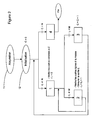
- An electronic analysis circuit aims to integrate into a passive matrix multicontact tactile sensor.
- the first fundamental element of said touch device is the touch sensor 1, necessary for the acquisition - the multicontact manipulation - using a capture interface 3.
- This capture interface 3 contains the electronic circuits for acquisition and control. analysis.
- Said touch sensor 1 is of the matrix type. Said sensor can be optionally divided into several parts in order to accelerate the capture, each part being scanned simultaneously.
- the data from the capture interface 3 is transmitted after filtering to the main processor 4.
- the main processor 4 also transmits to the graphical interface the data to be displayed on the display screen 2.
- This graphic interface can also be driven by a graphics processor 5.
- the touch sensor is controlled in the following way: one feeds successively, during a first phase of scanning, the tracks of one of the networks and the response is detected on each of the tracks of the second network.
- Contact zones corresponding to the nodes whose state is modified with respect to the idle state are determined as a function of these responses.
- One or more sets of adjacent nodes whose state is changed is determined. A set of such adjacent nodes defines a zone of contact. From this set of nodes is computed a position information qualified in the sense of the present cursor patent. In the case of several sets of nodes separated by non-active zones, several independent cursors will be determined during the same scanning phase.
- This information is refreshed periodically during new scan phases.
- Cursors are created, tracked or destroyed based on information obtained during successive scans.
- the cursor is for example calculated by a barycentre function of the contact zone.
- the general principle is to create as many sliders as there are zones detected on the touch sensor and to follow their evolution over time. When the user removes his fingers from the sensor, the associated sliders are destroyed. In this way, it is possible to capture the position and the evolution of several fingers on the touch sensor simultaneously.
- the actual measured electrical characteristic can be resistance or capacitance.
- the main processor 4 executes the program for associating the sensor data with graphic objects that are displayed on the display screen 2 in order to be manipulated.
- the figure 2 represents a diagram of the data acquisition process 11 over the entire touch sensor, implemented by the electronic circuit, with the columns as the supply axis and the lines as the detection axis.
- the sensor comprises M rows and N columns.
- This method has the function of determining the state of each node of the matrix sensor 1, namely whether said node is activated or not.
- Said method corresponds to the measurement of all the nodes of a "voltage" matrix.
- Said matrix is a matrix [M, N] containing at each point (I, J) the value of the voltage measured at the intersection point of line I and column J, with 1 ⁇ I ⁇ M and 1 ⁇ J ⁇ N. This matrix makes it possible to give the state of each of the points of the matrix sensor 1 at a given instant.
- the acquisition method 11 begins with an initialization step 12 of the data obtained during a previous acquisition.
- the axis of the columns constitutes the axis of supply and the axis of the lines constitutes the axis of detection.
- the line axis constitutes the feed axis and the axis of the columns constitutes the detection axis.
- the method 11 first scans the first column. It is powered for example in 5 volts.
- the electronic circuit measures an electrical characteristic at the point of intersection between said column and each of the lines from 1 to M.
- the process proceeds to the next column and resumes the measurements of electrical characteristics at the intersection of the new column considered and each of the lines from 1 to M.
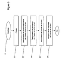
- the figure 3 represents a diagram of the data analysis method 21 used by the electronic circuit.
- the software is able to apply to the virtual graphic objects of the tactile electronic device the various specific processes in order to refresh said tactile electronic device in real time. Zones encompassing the contact areas, detected during the data acquisition step 11, are also defined.
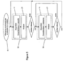
- the figure 4 represents a diagram of a method 31 of acquisition and analysis implemented by an electronic circuit according to a first example of operation.
- Said method 31 is a capacitive / resistive measurement alternating method, said alternation being periodic.
- the electronic circuit executes the step 32 corresponding to the succession of acquisition steps II and analysis 21 with the capacitance as the measured electrical characteristic.
- step 33 a new step 33 is performed, this step 33 corresponding to the succession acquisition steps 11 and analysis 21 with this time the resistance as the measured electrical characteristic.
- the method 31 performs a loop comprising the succession of steps 32 and 33. It thus alternates the measurements of electrical characteristics selected from the capacitance and the resistance.
- the method realizes K times the first step 32, then L times the second step 33, K and L being integers of which at least one is strictly greater than 1.
- the refresh rate is of the order of 100 Hz.
- the figure 5 represents a diagram of a method 41 of acquisition and analysis implemented by an electronic circuit according to a second example of operation.
- Said method 41 is a capacitive / resistive measurement alternating method, said alternation being conditioned by the possible detection of an artifact.
- the method 41 performs the steps 32 and 33.
- transition from one to the other of steps 32 and 33 is conditioned by the possible detection of an artefact resulting from each of the analysis steps 21 performed in steps 32 and 33.
- step 21 implemented during step 32 or 33, the electronic circuit determines whether an artefact-like parasitic phenomenon is present on at least a portion of the matrix sensor 1, the state data of each of which nodes were acquired and analyzed. If no artifact is detected at the output of step 32 or 33, then the process loops back to the same step. If an artifact has been detected, then the process alternates step.
- step 32 For example, if an artifact is not detected at the output of step 32, the method loops back to said step 32, but if an artifact is actually detected, the method alternates at step 33.
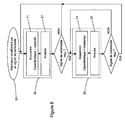
- the figure 6 represents a diagram of a method 51 of acquisition and analysis implemented by an electronic circuit according to a third example of operation.
- Said method 51 is a capacitive / resistive measurement alternating method, said alternation being conditioned by a control signal.
- the method performs steps 32 and 33.
- step 21 implemented during step 32 or 33, the electronic circuit determines whether it has received a control signal between said step and the previous one. If no control signal has been received, then the process loops back to the same step. If a control signal has been received, then the method alternates the step.
- step 32 For example, if a control signal has been received at the output of step 32, the method loops over said step 32, but if a control signal has actually been received, the method alternates on step 33.
- Such a control signal may for example be operated by the user of the multipoint tactile electronic device. Indeed, this user can use the capacitive measurement only in the case where his contact tool is a finger. If not, he is forced to use a resistive measure. Thus, when the user uses for example a stylus, he can activate a control signal delivering information in direction of the multi-touch sensor 1 so that the latter operates in a resistive measurement mode.
- the characteristic measured at each scanning phase is the resistance, point by point on the entire sensor (step 32).
- This capacitive measurement (step 14) on this slider - or contact zone - then provides, after analysis (step 21) and deduction (step 35), information on the nature of the contact, namely if the contact means is a finger (detected by a capacitive measurement) or a stylus (not detected by a capacitive measurement).
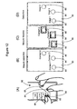
- a first contact 81 with a finger and a second contact with a stylus are detected on the touch screen 80 during a resistive measurement.
- Figure 9C and the chronogram of the figure 8 it is then proceeded to a capacitive measurement on these two contact areas 81 and 82.
- This measurement allows the detection of a contact in the area of the first contact 81 (finger) and does not obtain any detection on the area of the second contact 82 (stylus), as shown on the Figure 9D it is thus possible to discriminate between the two types of contacts, that is to say a finger 1 for the first contact 81 and a stylus 1 for the second contact 82.
- This capacitive measurement is done once on this created cursor ( figure 8 ), the nature of the contact constituted by this cursor can not a priori not change as long as it is maintained, and it is proceeded in parallel to scanning phases in resistive mode.
- This variant of the electronic analysis circuit makes it possible to determine the nature of the contact in order to take it into account, for example to adapt the accuracy of the next resistive measurement - the resolution to be greater for a stylus - or to reject a contact if its nature is not one that the touch sensor or part of it is likely to tolerate.
- the measurements are made in resistive mode on the entire sensor, point by point, at each scanning phase. If a release of the cursor corresponding to this contact is detected, a capacitive measurement is made on the cursor area in one block. This measurement makes it possible to determine whether the finger is always close to the relaxed contact zone, which is a sign of an unexpected release of the finger during prolonged contact (for example when handling a graphic object corresponding to a drop-down window).
- This variant of the electronic analysis circuit thus makes it possible not to lose a cursor defined by a finger when this loss of the cursor is not intentional.
- a capacitive measurement is performed on a graphic object to be secured, point by point, at each scanning phase (step 32). If a contact is detected according to this capacitive mode, a detection of the contact zone (step 13) is carried out, then a measurement in resistive mode (step 15) on the entire graphical object, which provides after analysis (step 21) information on the force exerted by the detected contact. It is then proceeded to the following deduction (step 35): if this force does not exceed a threshold value, the contact is insufficient and is not considered as a contact giving rise to the creation of a cursor. Otherwise, the cursor is created.
- This embodiment of the electronic analysis circuit makes it possible to avoid involuntary contact - for example a touch - being taken into account for a graphic object whose activation or not by contact is of fundamental importance.
- a multi-point tactile display incorporating an electronic analysis circuit has the advantage of combining the advantages of a capacitive measurement - better sensitivity of the "touch" - and of a resistive measurement - adaptation to any type of contact tool - without being constrained by the respective disadvantages.
- Such a multi-touch display is therefore able to provide in all circumstances optimal and complete information.
Landscapes
- Engineering & Computer Science (AREA)
- General Engineering & Computer Science (AREA)
- Theoretical Computer Science (AREA)
- Human Computer Interaction (AREA)
- Physics & Mathematics (AREA)
- General Physics & Mathematics (AREA)
- Position Input By Displaying (AREA)
- User Interface Of Digital Computer (AREA)
Applications Claiming Priority (2)
| Application Number | Priority Date | Filing Date | Title |
|---|---|---|---|
| FR0760015A FR2925714B1 (fr) | 2007-12-19 | 2007-12-19 | Circuit electronique d'analyse a alternance de mesure capacitive/resistive pour capteur tactile multicontacts a matrice passive |
| PCT/FR2008/001805 WO2009106736A1 (fr) | 2007-12-19 | 2008-12-19 | Circuit electronique d'analyse a alternance de mesure capacitive/ resistive pour capteur tactile multicontacts a matrice passive |
Publications (2)
| Publication Number | Publication Date |
|---|---|
| EP2235614A1 EP2235614A1 (fr) | 2010-10-06 |
| EP2235614B1 true EP2235614B1 (fr) | 2012-08-22 |
Family
ID=39580284
Family Applications (1)
| Application Number | Title | Priority Date | Filing Date |
|---|---|---|---|
| EP08872788A Not-in-force EP2235614B1 (fr) | 2007-12-19 | 2008-12-19 | Circuit electronique d'analyse a alternance de mesure capacitive/ resistive pour capteur tactile multicontacts a matrice passive |
Country Status (8)
| Country | Link |
|---|---|
| US (1) | US20100289508A1 (https=) |
| EP (1) | EP2235614B1 (https=) |
| JP (1) | JP2011507121A (https=) |
| KR (1) | KR20100098706A (https=) |
| CN (1) | CN101903855B (https=) |
| CA (1) | CA2709696A1 (https=) |
| FR (1) | FR2925714B1 (https=) |
| WO (1) | WO2009106736A1 (https=) |
Families Citing this family (20)
| Publication number | Priority date | Publication date | Assignee | Title |
|---|---|---|---|---|
| US9018030B2 (en) * | 2008-03-20 | 2015-04-28 | Symbol Technologies, Inc. | Transparent force sensor and method of fabrication |
| US8988191B2 (en) * | 2009-08-27 | 2015-03-24 | Symbol Technologies, Inc. | Systems and methods for pressure-based authentication of an input on a touch screen |
| KR101119373B1 (ko) * | 2010-07-09 | 2012-03-06 | 삼성전기주식회사 | 하이브리드 터치패널의 작동방법 |
| US8963874B2 (en) | 2010-07-31 | 2015-02-24 | Symbol Technologies, Inc. | Touch screen rendering system and method of operation thereof |
| CN103518176B (zh) * | 2011-05-12 | 2016-03-02 | 阿尔卑斯电气株式会社 | 输入装置及使用所述输入装置的多个点的载荷检测方法 |
| FR2976692B1 (fr) | 2011-06-17 | 2013-06-14 | Thales Sa | Dispositif tactile multicouches a detection capacitive multi-frequence. |
| KR101971067B1 (ko) * | 2011-08-31 | 2019-08-14 | 삼성전자 주식회사 | 휴대 단말기의 사용자 인터페이스 제공 방법 및 장치 |
| US20130050143A1 (en) * | 2011-08-31 | 2013-02-28 | Samsung Electronics Co., Ltd. | Method of providing of user interface in portable terminal and apparatus thereof |
| US10150144B2 (en) | 2011-12-08 | 2018-12-11 | Thomas P. Suiter | Hose handling system and methods of use |
| US9459160B2 (en) | 2012-06-13 | 2016-10-04 | Microsoft Technology Licensing, Llc | Input device sensor configuration |
| US9684382B2 (en) | 2012-06-13 | 2017-06-20 | Microsoft Technology Licensing, Llc | Input device configuration having capacitive and pressure sensors |
| JP5958215B2 (ja) * | 2012-09-12 | 2016-07-27 | 富士通株式会社 | 情報端末装置、タッチ座標決定方法及びタッチ座標決定プログラム |
| US10578499B2 (en) | 2013-02-17 | 2020-03-03 | Microsoft Technology Licensing, Llc | Piezo-actuated virtual buttons for touch surfaces |
| KR102100925B1 (ko) | 2013-03-22 | 2020-04-14 | 삼성전자주식회사 | 기판 구조체, 상기 기판 구조체를 형성하는 방법, 및 이를 구비하는 전기소자 |
| WO2014192710A1 (ja) * | 2013-05-28 | 2014-12-04 | 株式会社村田製作所 | タッチ式入力装置およびタッチ式入力検出方法 |
| GB2519581A (en) | 2013-10-28 | 2015-04-29 | Nokia Corp | An apparatus, method and computer program for sensing |
| US9448631B2 (en) | 2013-12-31 | 2016-09-20 | Microsoft Technology Licensing, Llc | Input device haptics and pressure sensing |
| US10416799B2 (en) | 2015-06-03 | 2019-09-17 | Microsoft Technology Licensing, Llc | Force sensing and inadvertent input control of an input device |
| US10222889B2 (en) | 2015-06-03 | 2019-03-05 | Microsoft Technology Licensing, Llc | Force inputs and cursor control |
| US10061385B2 (en) | 2016-01-22 | 2018-08-28 | Microsoft Technology Licensing, Llc | Haptic feedback for a touch input device |
Citations (1)
| Publication number | Priority date | Publication date | Assignee | Title |
|---|---|---|---|---|
| EP2026179A1 (en) * | 2007-08-10 | 2009-02-18 | IEE International Electronics & Engineering S.A.R.L. | Method of generating input data |
Family Cites Families (15)
| Publication number | Priority date | Publication date | Assignee | Title |
|---|---|---|---|---|
| US4686332A (en) * | 1986-06-26 | 1987-08-11 | International Business Machines Corporation | Combined finger touch and stylus detection system for use on the viewing surface of a visual display device |
| JPH0253132A (ja) * | 1988-08-18 | 1990-02-22 | Nippon Intaakeepu:Kk | タッチパネル |
| US5365461A (en) * | 1992-04-30 | 1994-11-15 | Microtouch Systems, Inc. | Position sensing computer input device |
| KR100300397B1 (ko) * | 1994-04-21 | 2001-10-22 | 김순택 | 터치판넬및디지타이저기능을겸비한시스템및구동방법 |
| EP0756733B1 (en) * | 1995-02-22 | 2002-09-18 | Koninklijke Philips Electronics N.V. | Low-cost resistive tablet with touch and stylus functionality |
| TW408277B (en) * | 1996-11-15 | 2000-10-11 | Alps Electric Co Ltd | Small current detector circuit and locator device using the same |
| US6762752B2 (en) * | 2001-11-29 | 2004-07-13 | N-Trig Ltd. | Dual function input device and method |
| DE602004027705D1 (de) * | 2003-02-10 | 2010-07-29 | N trig ltd | Berührungsdetektion für einen digitalisierer |
| FR2866726B1 (fr) | 2004-02-23 | 2006-05-26 | Jazzmutant | Controleur par manipulation d'objets virtuels sur un ecran tactile multi-contact |
| JP5172334B2 (ja) * | 2004-06-17 | 2013-03-27 | アドレア エルエルシー | タッチスクリーン上の2本指入力の使用 |
| TWI271645B (en) * | 2005-04-19 | 2007-01-21 | Elan Microelectronics Corp | Capacitive touchpad with a physical key function |
| US20070063876A1 (en) * | 2005-08-24 | 2007-03-22 | Wong Alex K | Multiple sensing element touch sensor |
| JP4408431B2 (ja) * | 2005-12-19 | 2010-02-03 | アルプス電気株式会社 | 入力装置 |
| US8018440B2 (en) * | 2005-12-30 | 2011-09-13 | Microsoft Corporation | Unintentional touch rejection |
| FR2925715B1 (fr) * | 2007-12-19 | 2010-06-18 | Stantum | Circuit electronique d'analyse a alternance axe d'alimentaiton/axe de detection pour capteur tactile multicontacts a matrice passive |
-
2007
- 2007-12-19 FR FR0760015A patent/FR2925714B1/fr not_active Expired - Fee Related
-
2008
- 2008-12-19 CA CA2709696A patent/CA2709696A1/fr not_active Abandoned
- 2008-12-19 CN CN2008801219926A patent/CN101903855B/zh not_active Expired - Fee Related
- 2008-12-19 JP JP2010538845A patent/JP2011507121A/ja active Pending
- 2008-12-19 EP EP08872788A patent/EP2235614B1/fr not_active Not-in-force
- 2008-12-19 KR KR1020107015950A patent/KR20100098706A/ko not_active Withdrawn
- 2008-12-19 WO PCT/FR2008/001805 patent/WO2009106736A1/fr not_active Ceased
- 2008-12-19 US US12/809,434 patent/US20100289508A1/en not_active Abandoned
Patent Citations (1)
| Publication number | Priority date | Publication date | Assignee | Title |
|---|---|---|---|---|
| EP2026179A1 (en) * | 2007-08-10 | 2009-02-18 | IEE International Electronics & Engineering S.A.R.L. | Method of generating input data |
Also Published As
| Publication number | Publication date |
|---|---|
| JP2011507121A (ja) | 2011-03-03 |
| FR2925714B1 (fr) | 2010-01-15 |
| WO2009106736A1 (fr) | 2009-09-03 |
| CA2709696A1 (fr) | 2009-09-03 |
| CN101903855A (zh) | 2010-12-01 |
| FR2925714A1 (fr) | 2009-06-26 |
| US20100289508A1 (en) | 2010-11-18 |
| EP2235614A1 (fr) | 2010-10-06 |
| KR20100098706A (ko) | 2010-09-08 |
| CN101903855B (zh) | 2013-08-07 |
Similar Documents
| Publication | Publication Date | Title |
|---|---|---|
| EP2235614B1 (fr) | Circuit electronique d'analyse a alternance de mesure capacitive/ resistive pour capteur tactile multicontacts a matrice passive | |
| EP2235615B1 (fr) | Circuit electronique d'analyse a modulation de caracteristiques de balayage pour capteur tactile multicontacts a matrice passive | |
| EP2310932B1 (fr) | Procédé d'acquisition et d'analyse d'un capteur tactile multicontacts suivant un principe dichotomique, circuit électronique et capteur tactile multicontacts mettant en oeuvre un tel procédé | |
| FR2925715A1 (fr) | Circuit electronique d'analyse a alternance axe d'alimentaiton/axe de detection pour capteur tactile multicontacts a matrice passive | |
| EP2956846B1 (fr) | Procédé, appareil et support de stockage pour naviguer dans un écran d'affichage | |
| EP2306279A2 (fr) | Dispositif d'acquisition d'informations tactiles à balayage séquentiel | |
| US10534464B2 (en) | Selective scanning for touch-sensitive display device | |
| EP1350218B1 (fr) | Procede et dispositif de reconnaissance de caracteres traces manuellement sur une zone de saisie | |
| FR2934921A1 (fr) | Capteur tactile multicontacts a moyens d'espacement de taille et impedance variables | |
| EP2235610A1 (fr) | Capteur tactile multicontacts avec mode veille monocontact | |
| EP2742409A1 (fr) | Procédé de caractérisation de toucher sur un écran tactile | |
| EP2769290B1 (fr) | Procède d'acquisition de données d'un capteur tactile matriciel, notamment pour un écran tactile | |
| CH698650B1 (fr) | Dispositif électronique de commande à touches tactiles destiné à remplir une fonction de curseur. | |
| FR2712103A1 (fr) | Instrument mobile orientable pour système numériseur électromagnétique. |
Legal Events
| Date | Code | Title | Description |
|---|---|---|---|
| PUAI | Public reference made under article 153(3) epc to a published international application that has entered the european phase |
Free format text: ORIGINAL CODE: 0009012 |
|
| 17P | Request for examination filed |
Effective date: 20100706 |
|
| AK | Designated contracting states |
Kind code of ref document: A1 Designated state(s): AT BE BG CH CY CZ DE DK EE ES FI FR GB GR HR HU IE IS IT LI LT LU LV MC MT NL NO PL PT RO SE SI SK TR |
|
| AX | Request for extension of the european patent |
Extension state: AL BA MK RS |
|
| RIN1 | Information on inventor provided before grant (corrected) |
Inventor name: JOGUET, PASCAL Inventor name: LARGILLIER, GUILLAUME Inventor name: OLIVIER, JULIEN |
|
| 17Q | First examination report despatched |
Effective date: 20101217 |
|
| DAX | Request for extension of the european patent (deleted) | ||
| GRAP | Despatch of communication of intention to grant a patent |
Free format text: ORIGINAL CODE: EPIDOSNIGR1 |
|
| GRAS | Grant fee paid |
Free format text: ORIGINAL CODE: EPIDOSNIGR3 |
|
| GRAA | (expected) grant |
Free format text: ORIGINAL CODE: 0009210 |
|
| RIN1 | Information on inventor provided before grant (corrected) |
Inventor name: JOGUET, PASCAL Inventor name: OLIVIER, JULIEN Inventor name: LARGILLIER, GUILLAUME |
|
| AK | Designated contracting states |
Kind code of ref document: B1 Designated state(s): AT BE BG CH CY CZ DE DK EE ES FI FR GB GR HR HU IE IS IT LI LT LU LV MC MT NL NO PL PT RO SE SI SK TR |
|
| REG | Reference to a national code |
Ref country code: GB Ref legal event code: FG4D Free format text: NOT ENGLISH |
|
| REG | Reference to a national code |
Ref country code: CH Ref legal event code: EP |
|
| REG | Reference to a national code |
Ref country code: IE Ref legal event code: FG4D Free format text: LANGUAGE OF EP DOCUMENT: FRENCH |
|
| REG | Reference to a national code |
Ref country code: AT Ref legal event code: REF Ref document number: 572281 Country of ref document: AT Kind code of ref document: T Effective date: 20120915 |
|
| REG | Reference to a national code |
Ref country code: DE Ref legal event code: R096 Ref document number: 602008018282 Country of ref document: DE Effective date: 20121018 |
|
| REG | Reference to a national code |
Ref country code: NL Ref legal event code: VDEP Effective date: 20120822 |
|
| REG | Reference to a national code |
Ref country code: AT Ref legal event code: MK05 Ref document number: 572281 Country of ref document: AT Kind code of ref document: T Effective date: 20120822 |
|
| REG | Reference to a national code |
Ref country code: LT Ref legal event code: MG4D Effective date: 20120822 |
|
| PG25 | Lapsed in a contracting state [announced via postgrant information from national office to epo] |
Ref country code: IS Free format text: LAPSE BECAUSE OF FAILURE TO SUBMIT A TRANSLATION OF THE DESCRIPTION OR TO PAY THE FEE WITHIN THE PRESCRIBED TIME-LIMIT Effective date: 20121222 Ref country code: HR Free format text: LAPSE BECAUSE OF FAILURE TO SUBMIT A TRANSLATION OF THE DESCRIPTION OR TO PAY THE FEE WITHIN THE PRESCRIBED TIME-LIMIT Effective date: 20120822 Ref country code: AT Free format text: LAPSE BECAUSE OF FAILURE TO SUBMIT A TRANSLATION OF THE DESCRIPTION OR TO PAY THE FEE WITHIN THE PRESCRIBED TIME-LIMIT Effective date: 20120822 Ref country code: FI Free format text: LAPSE BECAUSE OF FAILURE TO SUBMIT A TRANSLATION OF THE DESCRIPTION OR TO PAY THE FEE WITHIN THE PRESCRIBED TIME-LIMIT Effective date: 20120822 Ref country code: NO Free format text: LAPSE BECAUSE OF FAILURE TO SUBMIT A TRANSLATION OF THE DESCRIPTION OR TO PAY THE FEE WITHIN THE PRESCRIBED TIME-LIMIT Effective date: 20121122 Ref country code: LT Free format text: LAPSE BECAUSE OF FAILURE TO SUBMIT A TRANSLATION OF THE DESCRIPTION OR TO PAY THE FEE WITHIN THE PRESCRIBED TIME-LIMIT Effective date: 20120822 |
|
| PG25 | Lapsed in a contracting state [announced via postgrant information from national office to epo] |
Ref country code: PT Free format text: LAPSE BECAUSE OF FAILURE TO SUBMIT A TRANSLATION OF THE DESCRIPTION OR TO PAY THE FEE WITHIN THE PRESCRIBED TIME-LIMIT Effective date: 20121224 Ref country code: SI Free format text: LAPSE BECAUSE OF FAILURE TO SUBMIT A TRANSLATION OF THE DESCRIPTION OR TO PAY THE FEE WITHIN THE PRESCRIBED TIME-LIMIT Effective date: 20120822 Ref country code: SE Free format text: LAPSE BECAUSE OF FAILURE TO SUBMIT A TRANSLATION OF THE DESCRIPTION OR TO PAY THE FEE WITHIN THE PRESCRIBED TIME-LIMIT Effective date: 20120822 Ref country code: LV Free format text: LAPSE BECAUSE OF FAILURE TO SUBMIT A TRANSLATION OF THE DESCRIPTION OR TO PAY THE FEE WITHIN THE PRESCRIBED TIME-LIMIT Effective date: 20120822 Ref country code: GR Free format text: LAPSE BECAUSE OF FAILURE TO SUBMIT A TRANSLATION OF THE DESCRIPTION OR TO PAY THE FEE WITHIN THE PRESCRIBED TIME-LIMIT Effective date: 20121123 |
|
| PG25 | Lapsed in a contracting state [announced via postgrant information from national office to epo] |
Ref country code: NL Free format text: LAPSE BECAUSE OF FAILURE TO SUBMIT A TRANSLATION OF THE DESCRIPTION OR TO PAY THE FEE WITHIN THE PRESCRIBED TIME-LIMIT Effective date: 20120822 |
|
| PG25 | Lapsed in a contracting state [announced via postgrant information from national office to epo] |
Ref country code: DK Free format text: LAPSE BECAUSE OF FAILURE TO SUBMIT A TRANSLATION OF THE DESCRIPTION OR TO PAY THE FEE WITHIN THE PRESCRIBED TIME-LIMIT Effective date: 20120822 Ref country code: EE Free format text: LAPSE BECAUSE OF FAILURE TO SUBMIT A TRANSLATION OF THE DESCRIPTION OR TO PAY THE FEE WITHIN THE PRESCRIBED TIME-LIMIT Effective date: 20120822 Ref country code: CZ Free format text: LAPSE BECAUSE OF FAILURE TO SUBMIT A TRANSLATION OF THE DESCRIPTION OR TO PAY THE FEE WITHIN THE PRESCRIBED TIME-LIMIT Effective date: 20120822 Ref country code: ES Free format text: LAPSE BECAUSE OF FAILURE TO SUBMIT A TRANSLATION OF THE DESCRIPTION OR TO PAY THE FEE WITHIN THE PRESCRIBED TIME-LIMIT Effective date: 20121203 Ref country code: RO Free format text: LAPSE BECAUSE OF FAILURE TO SUBMIT A TRANSLATION OF THE DESCRIPTION OR TO PAY THE FEE WITHIN THE PRESCRIBED TIME-LIMIT Effective date: 20120822 |
|
| PG25 | Lapsed in a contracting state [announced via postgrant information from national office to epo] |
Ref country code: PL Free format text: LAPSE BECAUSE OF FAILURE TO SUBMIT A TRANSLATION OF THE DESCRIPTION OR TO PAY THE FEE WITHIN THE PRESCRIBED TIME-LIMIT Effective date: 20120822 Ref country code: IT Free format text: LAPSE BECAUSE OF FAILURE TO SUBMIT A TRANSLATION OF THE DESCRIPTION OR TO PAY THE FEE WITHIN THE PRESCRIBED TIME-LIMIT Effective date: 20120822 Ref country code: SK Free format text: LAPSE BECAUSE OF FAILURE TO SUBMIT A TRANSLATION OF THE DESCRIPTION OR TO PAY THE FEE WITHIN THE PRESCRIBED TIME-LIMIT Effective date: 20120822 |
|
| PLBE | No opposition filed within time limit |
Free format text: ORIGINAL CODE: 0009261 |
|
| STAA | Information on the status of an ep patent application or granted ep patent |
Free format text: STATUS: NO OPPOSITION FILED WITHIN TIME LIMIT |
|
| BERE | Be: lapsed |
Owner name: STANTUM Effective date: 20121231 |
|
| 26N | No opposition filed |
Effective date: 20130523 |
|
| PG25 | Lapsed in a contracting state [announced via postgrant information from national office to epo] |
Ref country code: MC Free format text: LAPSE BECAUSE OF NON-PAYMENT OF DUE FEES Effective date: 20121231 Ref country code: BG Free format text: LAPSE BECAUSE OF FAILURE TO SUBMIT A TRANSLATION OF THE DESCRIPTION OR TO PAY THE FEE WITHIN THE PRESCRIBED TIME-LIMIT Effective date: 20121122 |
|
| REG | Reference to a national code |
Ref country code: CH Ref legal event code: PL |
|
| GBPC | Gb: european patent ceased through non-payment of renewal fee |
Effective date: 20121219 |
|
| REG | Reference to a national code |
Ref country code: DE Ref legal event code: R097 Ref document number: 602008018282 Country of ref document: DE Effective date: 20130523 |
|
| REG | Reference to a national code |
Ref country code: IE Ref legal event code: MM4A |
|
| PG25 | Lapsed in a contracting state [announced via postgrant information from national office to epo] |
Ref country code: BE Free format text: LAPSE BECAUSE OF NON-PAYMENT OF DUE FEES Effective date: 20121231 |
|
| PG25 | Lapsed in a contracting state [announced via postgrant information from national office to epo] |
Ref country code: CH Free format text: LAPSE BECAUSE OF NON-PAYMENT OF DUE FEES Effective date: 20121231 Ref country code: LI Free format text: LAPSE BECAUSE OF NON-PAYMENT OF DUE FEES Effective date: 20121231 Ref country code: IE Free format text: LAPSE BECAUSE OF NON-PAYMENT OF DUE FEES Effective date: 20121219 |
|
| PG25 | Lapsed in a contracting state [announced via postgrant information from national office to epo] |
Ref country code: CY Free format text: LAPSE BECAUSE OF FAILURE TO SUBMIT A TRANSLATION OF THE DESCRIPTION OR TO PAY THE FEE WITHIN THE PRESCRIBED TIME-LIMIT Effective date: 20120822 Ref country code: MT Free format text: LAPSE BECAUSE OF FAILURE TO SUBMIT A TRANSLATION OF THE DESCRIPTION OR TO PAY THE FEE WITHIN THE PRESCRIBED TIME-LIMIT Effective date: 20120822 Ref country code: GB Free format text: LAPSE BECAUSE OF NON-PAYMENT OF DUE FEES Effective date: 20121219 |
|
| PGFP | Annual fee paid to national office [announced via postgrant information from national office to epo] |
Ref country code: DE Payment date: 20131210 Year of fee payment: 6 |
|
| PG25 | Lapsed in a contracting state [announced via postgrant information from national office to epo] |
Ref country code: TR Free format text: LAPSE BECAUSE OF FAILURE TO SUBMIT A TRANSLATION OF THE DESCRIPTION OR TO PAY THE FEE WITHIN THE PRESCRIBED TIME-LIMIT Effective date: 20120822 |
|
| PG25 | Lapsed in a contracting state [announced via postgrant information from national office to epo] |
Ref country code: LU Free format text: LAPSE BECAUSE OF NON-PAYMENT OF DUE FEES Effective date: 20121219 |
|
| PGFP | Annual fee paid to national office [announced via postgrant information from national office to epo] |
Ref country code: FR Payment date: 20131227 Year of fee payment: 6 |
|
| PG25 | Lapsed in a contracting state [announced via postgrant information from national office to epo] |
Ref country code: HU Free format text: LAPSE BECAUSE OF FAILURE TO SUBMIT A TRANSLATION OF THE DESCRIPTION OR TO PAY THE FEE WITHIN THE PRESCRIBED TIME-LIMIT Effective date: 20081219 |
|
| REG | Reference to a national code |
Ref country code: DE Ref legal event code: R119 Ref document number: 602008018282 Country of ref document: DE |
|
| REG | Reference to a national code |
Ref country code: FR Ref legal event code: ST Effective date: 20150831 |
|
| PG25 | Lapsed in a contracting state [announced via postgrant information from national office to epo] |
Ref country code: DE Free format text: LAPSE BECAUSE OF NON-PAYMENT OF DUE FEES Effective date: 20150701 |
|
| PG25 | Lapsed in a contracting state [announced via postgrant information from national office to epo] |
Ref country code: FR Free format text: LAPSE BECAUSE OF NON-PAYMENT OF DUE FEES Effective date: 20141231 |