EP2233608A1 - Pre-treatment process for electroless nickel plating - Google Patents
Pre-treatment process for electroless nickel plating Download PDFInfo
- Publication number
- EP2233608A1 EP2233608A1 EP09155882A EP09155882A EP2233608A1 EP 2233608 A1 EP2233608 A1 EP 2233608A1 EP 09155882 A EP09155882 A EP 09155882A EP 09155882 A EP09155882 A EP 09155882A EP 2233608 A1 EP2233608 A1 EP 2233608A1
- Authority
- EP
- European Patent Office
- Prior art keywords
- acid
- process according
- group
- nickel
- foregoing
- Prior art date
- Legal status (The legal status is an assumption and is not a legal conclusion. Google has not performed a legal analysis and makes no representation as to the accuracy of the status listed.)
- Granted
Links
Images



Classifications
-
- C—CHEMISTRY; METALLURGY
- C23—COATING METALLIC MATERIAL; COATING MATERIAL WITH METALLIC MATERIAL; CHEMICAL SURFACE TREATMENT; DIFFUSION TREATMENT OF METALLIC MATERIAL; COATING BY VACUUM EVAPORATION, BY SPUTTERING, BY ION IMPLANTATION OR BY CHEMICAL VAPOUR DEPOSITION, IN GENERAL; INHIBITING CORROSION OF METALLIC MATERIAL OR INCRUSTATION IN GENERAL
- C23C—COATING METALLIC MATERIAL; COATING MATERIAL WITH METALLIC MATERIAL; SURFACE TREATMENT OF METALLIC MATERIAL BY DIFFUSION INTO THE SURFACE, BY CHEMICAL CONVERSION OR SUBSTITUTION; COATING BY VACUUM EVAPORATION, BY SPUTTERING, BY ION IMPLANTATION OR BY CHEMICAL VAPOUR DEPOSITION, IN GENERAL
- C23C18/00—Chemical coating by decomposition of either liquid compounds or solutions of the coating forming compounds, without leaving reaction products of surface material in the coating; Contact plating
- C23C18/16—Chemical coating by decomposition of either liquid compounds or solutions of the coating forming compounds, without leaving reaction products of surface material in the coating; Contact plating by reduction or substitution, e.g. electroless plating
- C23C18/18—Pretreatment of the material to be coated
- C23C18/1803—Pretreatment of the material to be coated of metallic material surfaces or of a non-specific material surfaces
- C23C18/1824—Pretreatment of the material to be coated of metallic material surfaces or of a non-specific material surfaces by chemical pretreatment
- C23C18/1837—Multistep pretreatment
- C23C18/1841—Multistep pretreatment with use of metal first
-
- C—CHEMISTRY; METALLURGY
- C23—COATING METALLIC MATERIAL; COATING MATERIAL WITH METALLIC MATERIAL; CHEMICAL SURFACE TREATMENT; DIFFUSION TREATMENT OF METALLIC MATERIAL; COATING BY VACUUM EVAPORATION, BY SPUTTERING, BY ION IMPLANTATION OR BY CHEMICAL VAPOUR DEPOSITION, IN GENERAL; INHIBITING CORROSION OF METALLIC MATERIAL OR INCRUSTATION IN GENERAL
- C23C—COATING METALLIC MATERIAL; COATING MATERIAL WITH METALLIC MATERIAL; SURFACE TREATMENT OF METALLIC MATERIAL BY DIFFUSION INTO THE SURFACE, BY CHEMICAL CONVERSION OR SUBSTITUTION; COATING BY VACUUM EVAPORATION, BY SPUTTERING, BY ION IMPLANTATION OR BY CHEMICAL VAPOUR DEPOSITION, IN GENERAL
- C23C18/00—Chemical coating by decomposition of either liquid compounds or solutions of the coating forming compounds, without leaving reaction products of surface material in the coating; Contact plating
- C23C18/16—Chemical coating by decomposition of either liquid compounds or solutions of the coating forming compounds, without leaving reaction products of surface material in the coating; Contact plating by reduction or substitution, e.g. electroless plating
- C23C18/1601—Process or apparatus
- C23C18/1603—Process or apparatus coating on selected surface areas
- C23C18/1607—Process or apparatus coating on selected surface areas by direct patterning
-
- C—CHEMISTRY; METALLURGY
- C23—COATING METALLIC MATERIAL; COATING MATERIAL WITH METALLIC MATERIAL; CHEMICAL SURFACE TREATMENT; DIFFUSION TREATMENT OF METALLIC MATERIAL; COATING BY VACUUM EVAPORATION, BY SPUTTERING, BY ION IMPLANTATION OR BY CHEMICAL VAPOUR DEPOSITION, IN GENERAL; INHIBITING CORROSION OF METALLIC MATERIAL OR INCRUSTATION IN GENERAL
- C23C—COATING METALLIC MATERIAL; COATING MATERIAL WITH METALLIC MATERIAL; SURFACE TREATMENT OF METALLIC MATERIAL BY DIFFUSION INTO THE SURFACE, BY CHEMICAL CONVERSION OR SUBSTITUTION; COATING BY VACUUM EVAPORATION, BY SPUTTERING, BY ION IMPLANTATION OR BY CHEMICAL VAPOUR DEPOSITION, IN GENERAL
- C23C18/00—Chemical coating by decomposition of either liquid compounds or solutions of the coating forming compounds, without leaving reaction products of surface material in the coating; Contact plating
- C23C18/16—Chemical coating by decomposition of either liquid compounds or solutions of the coating forming compounds, without leaving reaction products of surface material in the coating; Contact plating by reduction or substitution, e.g. electroless plating
- C23C18/1601—Process or apparatus
- C23C18/1603—Process or apparatus coating on selected surface areas
- C23C18/1607—Process or apparatus coating on selected surface areas by direct patterning
- C23C18/1608—Process or apparatus coating on selected surface areas by direct patterning from pretreatment step, i.e. selective pre-treatment
-
- C—CHEMISTRY; METALLURGY
- C23—COATING METALLIC MATERIAL; COATING MATERIAL WITH METALLIC MATERIAL; CHEMICAL SURFACE TREATMENT; DIFFUSION TREATMENT OF METALLIC MATERIAL; COATING BY VACUUM EVAPORATION, BY SPUTTERING, BY ION IMPLANTATION OR BY CHEMICAL VAPOUR DEPOSITION, IN GENERAL; INHIBITING CORROSION OF METALLIC MATERIAL OR INCRUSTATION IN GENERAL
- C23C—COATING METALLIC MATERIAL; COATING MATERIAL WITH METALLIC MATERIAL; SURFACE TREATMENT OF METALLIC MATERIAL BY DIFFUSION INTO THE SURFACE, BY CHEMICAL CONVERSION OR SUBSTITUTION; COATING BY VACUUM EVAPORATION, BY SPUTTERING, BY ION IMPLANTATION OR BY CHEMICAL VAPOUR DEPOSITION, IN GENERAL
- C23C18/00—Chemical coating by decomposition of either liquid compounds or solutions of the coating forming compounds, without leaving reaction products of surface material in the coating; Contact plating
- C23C18/16—Chemical coating by decomposition of either liquid compounds or solutions of the coating forming compounds, without leaving reaction products of surface material in the coating; Contact plating by reduction or substitution, e.g. electroless plating
- C23C18/1601—Process or apparatus
- C23C18/1633—Process of electroless plating
- C23C18/1635—Composition of the substrate
- C23C18/1637—Composition of the substrate metallic substrate
-
- H—ELECTRICITY
- H05—ELECTRIC TECHNIQUES NOT OTHERWISE PROVIDED FOR
- H05K—PRINTED CIRCUITS; CASINGS OR CONSTRUCTIONAL DETAILS OF ELECTRIC APPARATUS; MANUFACTURE OF ASSEMBLAGES OF ELECTRICAL COMPONENTS
- H05K3/00—Apparatus or processes for manufacturing printed circuits
- H05K3/22—Secondary treatment of printed circuits
- H05K3/24—Reinforcing of the conductive pattern
- H05K3/244—Finish plating of conductors, especially of copper conductors, e.g. for pads or lands
-
- H—ELECTRICITY
- H05—ELECTRIC TECHNIQUES NOT OTHERWISE PROVIDED FOR
- H05K—PRINTED CIRCUITS; CASINGS OR CONSTRUCTIONAL DETAILS OF ELECTRIC APPARATUS; MANUFACTURE OF ASSEMBLAGES OF ELECTRICAL COMPONENTS
- H05K2203/00—Indexing scheme relating to apparatus or processes for manufacturing printed circuits covered by H05K3/00
- H05K2203/07—Treatments involving liquids, e.g. plating, rinsing
- H05K2203/0703—Plating
- H05K2203/0716—Metallic plating catalysts, e.g. for direct electroplating of through holes; Sensitising or activating metallic plating catalysts
-
- H—ELECTRICITY
- H05—ELECTRIC TECHNIQUES NOT OTHERWISE PROVIDED FOR
- H05K—PRINTED CIRCUITS; CASINGS OR CONSTRUCTIONAL DETAILS OF ELECTRIC APPARATUS; MANUFACTURE OF ASSEMBLAGES OF ELECTRICAL COMPONENTS
- H05K2203/00—Indexing scheme relating to apparatus or processes for manufacturing printed circuits covered by H05K3/00
- H05K2203/07—Treatments involving liquids, e.g. plating, rinsing
- H05K2203/0703—Plating
- H05K2203/072—Electroless plating, e.g. finish plating or initial plating
Definitions
- the present invention relates to a surface finishing process in manufacture of printed circuit boards (PCB).
- the inventive process suppresses extraneous nickel plating on a substrate having a copper patterned surface after activation with an ionic palladium activator.
- An activation of a copper surface prior to electroless nickel plating is required because copper is classified as a non-catalytic metal for electroless deposition of for example nickel deposited from hypophosphite containing electrolytes ( W. Riedel, Electroless Nickel Plating, ASM International, reprint 1998, p. 189 ).
- the purpose of the activation step is to deposit an immersion coating of a catalyst on the copper surface.
- the catalyst lowers the activation energy and allows the nickel to deposit on the copper surface. Examples of catalysts are palladium and ruthenium ( Printed Circuits Handbook, Ed.: C. F. Coombs, Jr., McGraw-Hill, 2001, p. 32.3 ).
- a palladium seed layer is immersion plated onto the copper surface, wherein the palladium ions are deposited onto the copper surface, reduced by copper to metallic state palladium and copper ions are released into the immersion plating bath.
- the substrate surface areas are then composed of metallic palladium and serve as seeds for the following electroless nickel plating.
- Extraneous nickel deposits have a weak adhesion on laminate and solder mask surfaces and can fracture off the PCB and also cause circuit shorts at other locations of the PCB.
- Nickel bridges between individual copper bond pads or copper trenches can directly result in circuit shorts.
- Nickel feet around a copper bond pad in fine line circuits also can cause circuit shorts by bridging individual copper bond pads.
- palladium ions or precipitates formed thereof adsorbed onto the copper bond pads should not be removed during the activation pre-treatment before electroless nickel plating in order to prevent skip plating.
- Skip plating is a phenomenon wherein an incomplete nickel plating occurs on the copper bond pads which leads to failures during bonding.
- US 2001/0040047 teaches a method which reduces bridging that can occur during plating. Said method comprises the following steps: contacting a circuitized substrate with a swelling agent, treating the substrate with a composition of an alkaline permanganate, a chromate or chlorite salt followed by applying a metal layer on the treated circuitized portion of the substrate.
- the method is an alternative to the process according to the present invention as no palladium ion activation is applied.
- the patent EP 0 707 093 discloses an activator which will selectively activate the copper surfaces for electroless nickel plating and thereby minimize or eliminate extraneous plating.
- Said activator composition comprises an imidazole compound and may further contain palladium ions.
- Excess palladium ions during activation of a copper surface tend to hydrolyze in the rinse step(s) applied before electroless plating of nickel and form palladium-containing precipitates.
- Said precipitates can be adsorbed onto surface areas of a PCB that are made of polymeric materials or can be trapped in cavities formed between structural features made of copper and polymeric materials, e.g., laminate, photoresist and/or solder mask on a PCB surface (see Figure 1 ).
- Said precipitates can get reduced to metallic state palladium by the reducing agent present in the successive electroless nickel plating bath. Nickel plating will occur on such reduced palladium precipitates. If the reduced palladium is present on surface areas of the PCB substrate other than the copper surface, unwanted extraneous nickel plating can occur and lead to circuit shorts.
- a rinse step after activation is required in order to remove all excess palladium ions before contacting the substrate with the electroless nickel plating composition.
- hydrolysis and precipitation of ionic palladium occurs preferably during such rinse steps. Therefore, at least one rinse step is done in a rinse solution consisting of diluted sulfuric acid. But in case of high density circuits the sulfuric acid rinse is not sufficient to remove the undesired palladium ions and palladium hydroxide precipitates. Extraneous nickel plating occurs during successive electroless nickel plating leading to circuit shorts.
- the deposition of ionic palladium or precipitates formed thereof shall only occur on surface areas of the PCB substrate designated for nickel plating.
- Said pre-treatment composition comprises at least two different types of acids wherein one type of acid is an amino carboxylic acid.
- the palladium ions and precipitates formed thereof can be easily rinsed off from the plastic material surface of the PCB substrate by contacting the PCB substrate after activation with the pre-treatment composition according to the invention. Extraneous nickel plating in areas of the PCB substrate surface not desired for nickel plating is then suppressed.
- the process for deposition of electroless nickel according to the present invention comprises the following steps:
- compositions for activation of copper surfaces for electroless nickel plating are well known in the art ( K. Johal, SMTA International, Chicago, October 2001, Proceedings of the Technical Program, 612-620 ). Acidic solutions of palladium ions are frequently applied for said purpose. Such solutions comprise at least one acid, at least one source of palladium ions and optionally a surfactant.
- the at least one acid is selected from the group comprising hydrochloric acid, sulfuric acid, toluene sulfonic acid and methane sulfonic acid.
- the concentration of the at least one acid preferably ranges from 25 g to 150 g/l, more preferred 50 g/l to 100 g/l.
- the at least one source of palladium ions preferably is selected from the group comprising palladium chloride, palladium sulphate and palladium acetate.
- the concentration of the at least one source of palladium ions ranges from 10 mg/l to 100 mg/l, more preferred from 30 mg/l to 70 mg/l.
- the PCB substrate is contacted with such an activator solution at a temperature in the range of 10 °C to 40 °C, more preferred 20 °C to 30 °C for 30 s to 300 s, more preferred 60 s to 240 s.
- the pre-treatment composition for electroless nickel plating comprises a mixture of at least two different types of acids, wherein one type of acid is an organic amino carboxylic acid.
- the at least one amino carboxylic acid is selected from compounds represented by formula 1 or formula 2: wherein R11, R12, R21 and R22 are independently selected from the group consisting of H, C 1 -C 4 alkyl, linear or branched; R31, R32, R33, R34 and R35 are independently selected from the group consisting of H, phenyl, benzyl, C 1 -C 4 alkyl, linear or branched, substituted or unsubstituted, wherein the substituents are selected from the group consisting of -OH, -SH, -NH 2 , -COOH; R41 and R42 are independently selected from the group consisting of H, C 1 -C 4 alkyl, linear or branched, or a suitable counter ion for example Na + , K + , NH 4 + .
- R11, R12, R21 and R22 are selected from H, methyl and ethyl.
- R31, R32, R33, R34 and R35 are independently selected from the group consisting of H, methyl, ethyl, -CH 2 OH, -CH 2 NH 2 , -CH 2 COOH, -CH 2 CH 2 OH, -CH 2 CH 2 NH 2 , -CH 2 CH 2 COOH, -CH 2 SH, -CH 2 CH 2 SH and -CH 2 CONH 2 .
- Preferred organic amino carboxylic acids are selected from the group consisting of alanine, asparagine, aspartic acid, cysteine, glutamic acid, glycine, isoleucine, leucine, lysine, serine, methionine, threonine, valine, N,N-dimethyl glycine, ⁇ -alanine, ⁇ -leucine, ⁇ -isoleucine, ⁇ -glutamine, ⁇ -glutamic acid, ⁇ -methionine, ⁇ -asparagic acid.
- the at least one amino carboxylic acid is present in the pre-treatment composition in a concentration of 0.1 g/l to 100 g/l, more preferred 0.5 g/l to 50 g/l and most preferred 1 g/l to 15 g/l.
- the at least one acid present in the pre-treatment composition which is not an amino carboxylic acid preferably can be selected from the group consisting of sulfuric acid, hydrochloric acid, toluene sulfonic acid, methane sulfonic acid, formic acid and acetic acid.
- the total amount of acids which are not organic amino carboxylic acids ranges from 25 g/l to 150 g/l, more preferred from 50 g/l to 100 g/l.
- the most preferred mixture of acids in the pre-treatment composition consists of sulphuric acid and an organic amino carboxylic acid.
- the pre-treatment composition according to the present invention may further contain a surfactant.
- the pH value of the pre-treatment composition is preferably ⁇ 1.
- At least one additional rinse step between process steps i. and ii. using essentially water is optional.
- At least one additional rinse step between process step ii. and iii. Is applied using essentially water is mandatory.
- the substrate having an activated copper surface is contacted with the inventive pre-treatment composition at a temperature of 10 °C to 50 °C, more preferred 15 °C to 40 °C.
- the contact time ranges from 30 s to 10 min, more preferred 1 min to 6 min.
- a PCB substrate 2 having electroplated copper bond pads was contacted with an activator composition comprising 50 mg/l Pd 2+ ions and 90 g/l sulfuric acid at a temperature of 23 °C for 3 min.
- said substrate was rinsed with a pre-treatment solution consisting of 60 g/l sulfuric acid at 20 °C for 5 min and then rinsed with water.
- nickel was deposited from an electroless nickel electrolyte (Aurotech ® CNN, a product of Atotech Deutschland GmbH). The substrate surface was then investigated with an optical microscope ( Figure 2 ). Extraneous nickel plating 6 occurred around nickel coated copper bond pads 5.
- a PCB substrate having electroplated copper and solder mask surface areas was contacted with an activator composition comprising 50 mg/l Pd 2+ ions and 90 g/l sulfuric acid at a temperature of 23 °C for 3 min.
- said substrate was rinsed with a pre-treatment solution consisting of 60 g/l sulfuric acid and 3 g/l alanine at 20 °C for 5 min and then rinsed with water.
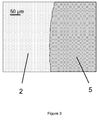
- nickel was deposited from an electroless nickel electrolyte (Aurotech ® CNN, a product of Atotech Deutschland GmbH). The substrate surface was then investigated with an optical microscope ( Figure 3 ). No extraneous nickel plating occurred on the PCB substrate 2 around nickel coated copper bond pads 5.
- Copper bond pads 1 on the surface of a PCB substrate 2 were activated with a solution of palladium ions comprising 50 mg/l Pd 2+ ions and 90 g/l sulfuric acid at a temperature of 23 °C for 3 min.
- said substrate was rinsed with a pre-treatment solution consisting of 60 g/l sulfuric acid at 20 °C for 5 min and then rinsed with water.
- nickel was deposited from an electroless nickel electrolyte (Aurotech ® CNN, a product of Atotech Deutschland GmbH) and coated with a thin gold layer from an immersion gold electrolyte (Aurotech ® SF Plus, a product of Atotech GmbH).
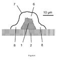
- FIG. 4 One typical nickel foot 8 observed is shown in Figure 4 .
- the nickel foot 8 has a width which is about 200 % of the deposited nickel coating 6 on the copper bond pad 1.
- Copper bond pads 1 on the surface of a PCB substrate 2 were activated with a solution of palladium ions as described in example 3, rinsed with water and then contacted with an inventive pre-treatment composition consisting of 60 g/l sulfuric acid and 3 g/l alanine, rinsed with water and then coated with nickel and gold as described in example 3.
- Cross-sections of nickel 6 and gold 7 coated copper bond pads 1 were made and investigated with a scanning electron microscope (SEM) in order to determine the nickel foot 8 around copper bonding pads 1.
- SEM scanning electron microscope
Landscapes
- Chemical & Material Sciences (AREA)
- Engineering & Computer Science (AREA)
- Chemical Kinetics & Catalysis (AREA)
- Organic Chemistry (AREA)
- Metallurgy (AREA)
- General Chemical & Material Sciences (AREA)
- Materials Engineering (AREA)
- Mechanical Engineering (AREA)
- Microelectronics & Electronic Packaging (AREA)
- Manufacturing & Machinery (AREA)
- Chemically Coating (AREA)
- Manufacturing Of Printed Wiring (AREA)
- Life Sciences & Earth Sciences (AREA)
- Oil, Petroleum & Natural Gas (AREA)
- Wood Science & Technology (AREA)
- Inorganic Chemistry (AREA)
Abstract
Description
- The present invention relates to a surface finishing process in manufacture of printed circuit boards (PCB). The inventive process suppresses extraneous nickel plating on a substrate having a copper patterned surface after activation with an ionic palladium activator.
- Surface finishing processes in the manufacture of printed circuit boards add bondable surfaces areas to a printed circuit board where active and passive components can be mechanically and electrically contacted to the PCB. Frequently applied surface finishing processes are the ENIG process (Electroless Nickel Immersion Gold) and Ni/Pd(/Au) processes. In both types of processes, a copper surface of a printed circuit board is activated with an activation composition containing a noble metal ion followed by electroless deposition of nickel.
- An activation of a copper surface prior to electroless nickel plating is required because copper is classified as a non-catalytic metal for electroless deposition of for example nickel deposited from hypophosphite containing electrolytes (W. Riedel, Electroless Nickel Plating, ASM International, reprint 1998, p. 189). The purpose of the activation step is to deposit an immersion coating of a catalyst on the copper surface. The catalyst lowers the activation energy and allows the nickel to deposit on the copper surface. Examples of catalysts are palladium and ruthenium (Printed Circuits Handbook, Ed.: C. F. Coombs, Jr., McGraw-Hill, 2001, p. 32.3). Usually, a palladium seed layer is immersion plated onto the copper surface, wherein the palladium ions are deposited onto the copper surface, reduced by copper to metallic state palladium and copper ions are released into the immersion plating bath. The substrate surface areas are then composed of metallic palladium and serve as seeds for the following electroless nickel plating.
- It is important to rinse the substrate carefully between activation of the copper surface and electroless nickel plating to remove all excessive noble metal ions. Otherwise precipitates formed of noble metal hydroxides can lead to extraneous (uncontrolled) nickel deposition around individual copper features on the substrate surface and surfaces made of plastic materials. The phrase 'plastic materials' comprises bare PCB laminates, solder masks and photoimageable resists such as dry film resists. The noble metal hydroxide precipitates serve as seeds for uncontrolled deposition of nickel. Typical phenomena of extraneous nickel plating are nickel bridges and nickel feet. Extraneous nickel plating can lead for example to circuit shorts, especially in high density circuits with line and space widths of 75 µm or less. Extraneous nickel deposits have a weak adhesion on laminate and solder mask surfaces and can fracture off the PCB and also cause circuit shorts at other locations of the PCB. Nickel bridges between individual copper bond pads or copper trenches can directly result in circuit shorts. Nickel feet around a copper bond pad in fine line circuits also can cause circuit shorts by bridging individual copper bond pads. In addition, palladium ions or precipitates formed thereof adsorbed onto the copper bond pads should not be removed during the activation pre-treatment before electroless nickel plating in order to prevent skip plating. Skip plating is a phenomenon wherein an incomplete nickel plating occurs on the copper bond pads which leads to failures during bonding.
- The problem of extraneous plating of nickel is solved in the prior art by different approaches:
- Watanabe et al. investigated ionic palladium activators containing ammonium chloride as a complexing agent and sodium dodecyl sulfate as a surfactant.
- They claim a negatively charged palladium-chloro complex as the active component in their activator composition which is repulsed by the negatively charged surfactant preferably adsorbed on the dielectric surface areas surrounding the copper bond pads (K. Watanabe, T. Nishiwaki, H. Honma, International Society of Electrochemistry-55th Annual Meeting, Thessaloniki, 19-24 September 2004).
-
US 2001/0040047 teaches a method which reduces bridging that can occur during plating. Said method comprises the following steps: contacting a circuitized substrate with a swelling agent, treating the substrate with a composition of an alkaline permanganate, a chromate or chlorite salt followed by applying a metal layer on the treated circuitized portion of the substrate. The method is an alternative to the process according to the present invention as no palladium ion activation is applied. - The patent
EP 0 707 093 discloses an activator which will selectively activate the copper surfaces for electroless nickel plating and thereby minimize or eliminate extraneous plating. Said activator composition comprises an imidazole compound and may further contain palladium ions. - Excess palladium ions during activation of a copper surface tend to hydrolyze in the rinse step(s) applied before electroless plating of nickel and form palladium-containing precipitates. Said precipitates can be adsorbed onto surface areas of a PCB that are made of polymeric materials or can be trapped in cavities formed between structural features made of copper and polymeric materials, e.g., laminate, photoresist and/or solder mask on a PCB surface (see
Figure 1 ). Said precipitates can get reduced to metallic state palladium by the reducing agent present in the successive electroless nickel plating bath. Nickel plating will occur on such reduced palladium precipitates. If the reduced palladium is present on surface areas of the PCB substrate other than the copper surface, unwanted extraneous nickel plating can occur and lead to circuit shorts. - A rinse step after activation is required in order to remove all excess palladium ions before contacting the substrate with the electroless nickel plating composition. On the other hand, hydrolysis and precipitation of ionic palladium occurs preferably during such rinse steps. Therefore, at least one rinse step is done in a rinse solution consisting of diluted sulfuric acid. But in case of high density circuits the sulfuric acid rinse is not sufficient to remove the undesired palladium ions and palladium hydroxide precipitates. Extraneous nickel plating occurs during successive electroless nickel plating leading to circuit shorts.
-
-
Figure 1 shows a schematic cross section of a PCB. Acopper bond pad 1 deposited on aPCB substrate 2 and asolder mask 3 form acavity 4 betweencopper bond pad 1 andsolder mask 3. Palladium ions and/or precipitates formed thereof may be trapped incavity 4 and may not be removed during rinse steps between activation and electroless nickel plating. Said trapped palladium ions and/or precipitates formed thereof may serve as seeds for extraneous nickel plating and lead to a nickel foot aroundcopper bond pad 1. -
Figure 2 shows a top view of a copper bond pad with anickel deposit 5 on aPCB substrate 2 with extraneous nickel plating 6 around the nickel coated copper bond pad 5 (Example 1). -
Figure 3 shows a top view of a copper bond pad with anickel deposit 5 on aPCB substrate 2 without extraneous nickel plating.Substrate 2 was contacted with the inventive pre-treatment composition prior to electroless nickel plating (Example 2). -
Figure 4 shows acopper bond pad 1 on aPCB substrate 2 having anickel coating 6 and agold coating 7 derived from comparative Example 3. Thenickel foot 8 has a widths almost double as that of the desirednickel coating 6. -
Figure 5 shows acopper bond pad 1 on aPCB substrate 2 having anickel coating 6 and agold coating 7 derived from Example 4. The widths of thenickel foot 8 is reduced by 2/3 compared to Example 3. - It is an object of the present invention to provide a process for electroless deposition of nickel onto a copper surface of a PCB substrate which suppresses extraneous nickel plating.
- The deposition of ionic palladium or precipitates formed thereof shall only occur on surface areas of the PCB substrate designated for nickel plating. This can be achieved by applying the inventive pre-treatment composition for electroless nickel plating. Said pre-treatment composition comprises at least two different types of acids wherein one type of acid is an amino carboxylic acid. The palladium ions and precipitates formed thereof can be easily rinsed off from the plastic material surface of the PCB substrate by contacting the PCB substrate after activation with the pre-treatment composition according to the invention. Extraneous nickel plating in areas of the PCB substrate surface not desired for nickel plating is then suppressed.
- The process for deposition of electroless nickel according to the present invention comprises the following steps:
- i. contacting a substrate containing a copper surface with a noble metal ion containing composition; thereafter
- ii. contacting the copper containing surface with a composition comprising an organic amino carboxylic acid; and
- iii. electroless plating of nickel onto said treated copper containing surface.
- Compositions for activation of copper surfaces for electroless nickel plating are well known in the art (K. Johal, SMTA International, Chicago, October 2001, Proceedings of the Technical Program, 612-620). Acidic solutions of palladium ions are frequently applied for said purpose. Such solutions comprise at least one acid, at least one source of palladium ions and optionally a surfactant. The at least one acid is selected from the group comprising hydrochloric acid, sulfuric acid, toluene sulfonic acid and methane sulfonic acid. The concentration of the at least one acid preferably ranges from 25 g to 150 g/l, more preferred 50 g/l to 100 g/l. The at least one source of palladium ions preferably is selected from the group comprising palladium chloride, palladium sulphate and palladium acetate. The concentration of the at least one source of palladium ions ranges from 10 mg/l to 100 mg/l, more preferred from 30 mg/l to 70 mg/l. The PCB substrate is contacted with such an activator solution at a temperature in the range of 10 °C to 40 °C, more preferred 20 °C to 30 °C for 30 s to 300 s, more preferred 60 s to 240 s.
- The pre-treatment composition for electroless nickel plating comprises a mixture of at least two different types of acids, wherein one type of acid is an organic amino carboxylic acid.
- In one embodiment of the invention, the at least one amino carboxylic acid is selected from compounds represented by
formula 1 or formula 2:
- Preferably R11, R12, R21 and R22 are selected from H, methyl and ethyl. Preferably R31, R32, R33, R34 and R35 are independently selected from the group consisting of H, methyl, ethyl, -CH2OH, -CH2NH2, -CH2COOH, -CH2CH2OH, -CH2CH2NH2, -CH2CH2COOH, -CH2SH, -CH2CH2SH and -CH2CONH2.
- Preferred organic amino carboxylic acids are selected from the group consisting of alanine, asparagine, aspartic acid, cysteine, glutamic acid, glycine, isoleucine, leucine, lysine, serine, methionine, threonine, valine, N,N-dimethyl glycine, β-alanine, β-leucine, β-isoleucine, β-glutamine, β-glutamic acid, β-methionine, β-asparagic acid.
- The at least one amino carboxylic acid is present in the pre-treatment composition in a concentration of 0.1 g/l to 100 g/l, more preferred 0.5 g/l to 50 g/l and most preferred 1 g/l to 15 g/l.
- The at least one acid present in the pre-treatment composition which is not an amino carboxylic acid preferably can be selected from the group consisting of sulfuric acid, hydrochloric acid, toluene sulfonic acid, methane sulfonic acid, formic acid and acetic acid. The total amount of acids which are not organic amino carboxylic acids ranges from 25 g/l to 150 g/l, more preferred from 50 g/l to 100 g/l. The most preferred mixture of acids in the pre-treatment composition consists of sulphuric acid and an organic amino carboxylic acid.
- The pre-treatment composition according to the present invention may further contain a surfactant.
- The pH value of the pre-treatment composition is preferably < 1.
- At least one additional rinse step between process steps i. and ii. using essentially water is optional. At least one additional rinse step between process step ii. and iii. Is applied using essentially water is mandatory.
- The substrate having an activated copper surface is contacted with the inventive pre-treatment composition at a temperature of 10 °C to 50 °C, more preferred 15 °C to 40 °C. The contact time ranges from 30 s to 10 min, more preferred 1 min to 6 min.
- There is no risk of nickel skip plating as re-dissolution of palladium from the copper surface does not occur when contacting the PCB substrate with the inventive pre-treatment composition. Skip plating means a lack of electroless nickel plating on copper surface areas where the copper is not sufficiently activated. Furthermore, the pre-treatment composition is very tolerant against drag over from the activator tank.
- The invention will now be illustrated by reference to the following non-limiting examples.
- A
PCB substrate 2 having electroplated copper bond pads was contacted with an activator composition comprising 50 mg/l Pd2+ ions and 90 g/l sulfuric acid at a temperature of 23 °C for 3 min. In the next step said substrate was rinsed with a pre-treatment solution consisting of 60 g/l sulfuric acid at 20 °C for 5 min and then rinsed with water. As the final step nickel was deposited from an electroless nickel electrolyte (Aurotech® CNN, a product of Atotech Deutschland GmbH). The substrate surface was then investigated with an optical microscope (Figure 2 ). Extraneous nickel plating 6 occurred around nickel coatedcopper bond pads 5. - A PCB substrate having electroplated copper and solder mask surface areas was contacted with an activator composition comprising 50 mg/l Pd2+ ions and 90 g/l sulfuric acid at a temperature of 23 °C for 3 min. In the next step said substrate was rinsed with a pre-treatment solution consisting of 60 g/l sulfuric acid and 3 g/l alanine at 20 °C for 5 min and then rinsed with water. As the final step nickel was deposited from an electroless nickel electrolyte (Aurotech® CNN, a product of Atotech Deutschland GmbH). The substrate surface was then investigated with an optical microscope (
Figure 3 ). No extraneous nickel plating occurred on thePCB substrate 2 around nickel coatedcopper bond pads 5. -
Copper bond pads 1 on the surface of aPCB substrate 2 were activated with a solution of palladium ions comprising 50 mg/l Pd2+ ions and 90 g/l sulfuric acid at a temperature of 23 °C for 3 min. In the next step said substrate was rinsed with a pre-treatment solution consisting of 60 g/l sulfuric acid at 20 °C for 5 min and then rinsed with water. As the final step nickel was deposited from an electroless nickel electrolyte (Aurotech® CNN, a product of Atotech Deutschland GmbH) and coated with a thin gold layer from an immersion gold electrolyte (Aurotech® SF Plus, a product of Atotech Deutschland GmbH). Cross-sections ofnickel 6 andgold 7 coatedcopper bond pads 1 were made and investigated with a scanning electron microscope (SEM) in order to determine thenickel foot 8 aroundcopper bonding pads 1. Onetypical nickel foot 8 observed is shown inFigure 4 . Thenickel foot 8 has a width which is about 200 % of the depositednickel coating 6 on thecopper bond pad 1. -
Copper bond pads 1 on the surface of aPCB substrate 2 were activated with a solution of palladium ions as described in example 3, rinsed with water and then contacted with an inventive pre-treatment composition consisting of 60 g/l sulfuric acid and 3 g/l alanine, rinsed with water and then coated with nickel and gold as described in example 3. Cross-sections ofnickel 6 andgold 7 coatedcopper bond pads 1 were made and investigated with a scanning electron microscope (SEM) in order to determine thenickel foot 8 aroundcopper bonding pads 1. Onetypical nickel foot 8 observed is shown inFigure 5 and has a width which is about 133 % of the depositednickel coating 6 on thecopper bond pad 1.
Claims (12)
- A process for deposition of electroless nickel comprising the following steps:i. contacting a substrate containing a copper surface with a noble metal ion containing composition; thereafterii. contacting the copper containing surface with a composition comprising an organic amino carboxylic acid; andiii. electroless plating of nickel onto said treated copper containing surface.
- The process according to claim 1 wherein the noble metal ion is palladium.
- The process according to any of the foregoing claims wherein the pre-treatment composition in step ii. further comprises an acid selected from the group consisting of sulfuric acid, hydrochloric acid, toluene sulfonic acid, methane sulfonic acid, formic acid and acetic acid.
- The process according to claim 3 wherein the concentration of the further acid ranges from 25 g/l to 150 g/l.
- The process according to any of the foregoing claims wherein the pre-treatment composition contains at least one amino carboxylic acid represented by formula 1 and formula 2:

- The process according to claim 5, wherein the suitable counter ion is selected from the group consisting of Na+, K+, NH4 +.
- The process according to any of the foregoing claims, wherein R11, R12, R21 and R22 are selected independently from H, methyl and ethyl.
- The process according to any of the foregoing claims, wherein R31, R32, R33, R34 and R35 are independently selected from the group consisting of H, methyl, ethyl, -CH2OH, -CH2NH2, -CH2COOH, -CH2CH2OH, -CH2CH2NH2, -CH2CH2COOH, -CH2SH, -CH2CH2SH and -CH2CONH2.
- The process according to any of the foregoing claims, wherein the organic amino carboxylic acid is selected from the group consisting of alanine, asparagine, aspartic acid, cysteine, glutamic acid, glycine, isoleucine, leucine, lysine, serine, phenylalanine, methionine, threonine, valine, N,N-dimethyl glycine.
- The process according to claim 1 wherein the organic amino carboxylic acid is selected from the group consisting of β-alanine, β-leucine, β-isoleucine, β-glutamine, β-glutamic acid, β-methionine, β-asparagic acid
- The process according to any of the foregoing claims, wherein the concentration of the at least one amino carboxylic acid ranges from 0.1 g/l to 100 g/l.
- The process according to any of the foregoing claims, wherein the copper surface is on a printed circuit board substrate.
Priority Applications (8)
| Application Number | Priority Date | Filing Date | Title |
|---|---|---|---|
| EP09155882.5A EP2233608B1 (en) | 2009-03-23 | 2009-03-23 | Pre-treatment process for electroless nickel plating |
| CN2010800137748A CN102405306B (en) | 2009-03-23 | 2010-03-12 | Pretreatment method of electroless nickel plating |
| KR1020167003442A KR101630597B1 (en) | 2009-03-23 | 2010-03-12 | Pre-treatment process for electroless nickel plating |
| US13/254,239 US20120321781A1 (en) | 2009-03-23 | 2010-03-12 | Pre-treatment process for electroless nickel plating |
| PCT/EP2010/053188 WO2010108795A1 (en) | 2009-03-23 | 2010-03-12 | Pre-treatment process for electroless nickel plating |
| JP2012501236A JP5570585B2 (en) | 2009-03-23 | 2010-03-12 | Pretreatment method for electroless nickel plating |
| KR1020117022178A KR20110130442A (en) | 2009-03-23 | 2010-03-12 | Pretreatment method for electroless nickel plating |
| TW099108408A TWI480419B (en) | 2009-03-23 | 2010-03-22 | Pretreatment method for electroless nickel plating |
Applications Claiming Priority (1)
| Application Number | Priority Date | Filing Date | Title |
|---|---|---|---|
| EP09155882.5A EP2233608B1 (en) | 2009-03-23 | 2009-03-23 | Pre-treatment process for electroless nickel plating |
Publications (2)
| Publication Number | Publication Date |
|---|---|
| EP2233608A1 true EP2233608A1 (en) | 2010-09-29 |
| EP2233608B1 EP2233608B1 (en) | 2016-03-23 |
Family
ID=41334378
Family Applications (1)
| Application Number | Title | Priority Date | Filing Date |
|---|---|---|---|
| EP09155882.5A Not-in-force EP2233608B1 (en) | 2009-03-23 | 2009-03-23 | Pre-treatment process for electroless nickel plating |
Country Status (7)
| Country | Link |
|---|---|
| US (1) | US20120321781A1 (en) |
| EP (1) | EP2233608B1 (en) |
| JP (1) | JP5570585B2 (en) |
| KR (2) | KR20110130442A (en) |
| CN (1) | CN102405306B (en) |
| TW (1) | TWI480419B (en) |
| WO (1) | WO2010108795A1 (en) |
Cited By (2)
| Publication number | Priority date | Publication date | Assignee | Title |
|---|---|---|---|---|
| EP2910666A1 (en) | 2014-02-21 | 2015-08-26 | ATOTECH Deutschland GmbH | Pre-treatment process for electroless plating |
| CN117620164A (en) * | 2023-12-28 | 2024-03-01 | 安徽壹石通材料科学研究院有限公司 | A kind of silver-plated nickel powder and its industrial preparation method and application |
Families Citing this family (12)
| Publication number | Priority date | Publication date | Assignee | Title |
|---|---|---|---|---|
| US9783890B2 (en) | 2012-10-26 | 2017-10-10 | Rohm And Haas Electronic Materials Llc | Process for electroless plating and a solution used for the same |
| CN103945654A (en) * | 2013-01-18 | 2014-07-23 | 北大方正集团有限公司 | Method for leaving palladium ions in non-metallized holes of passivation circuit board and circuit board manufactured through same |
| CN104470236B (en) * | 2013-09-16 | 2017-10-10 | 深圳市兴经纬科技开发有限公司 | The rear immersion liquid of circuit board chemical nickel plating gold and rear leaching method |
| CN103556134B (en) * | 2013-11-13 | 2015-11-25 | 湖南省化讯应用材料有限公司 | The pretreatment process of process for electroless nickel plating |
| CN104878422B (en) * | 2014-02-28 | 2017-12-12 | 比亚迪股份有限公司 | A kind of activation method of palladium activating solution and preparation method thereof and plastics |
| CN103981514A (en) * | 2014-06-11 | 2014-08-13 | 深圳市兴经纬科技开发有限公司 | Circuit board chemical nickel plating activation fluid and activation method |
| US20170191165A1 (en) * | 2015-03-24 | 2017-07-06 | Om Sangyo Co., Ltd. | Method for producing plated article |
| US20160348245A1 (en) * | 2015-05-28 | 2016-12-01 | Macdermid, Incorporated | Method of Pretreatment for Electroless Plating |
| LT6899B (en) | 2020-08-27 | 2022-04-11 | Valstybinis mokslinių tyrimų institutas Fizinių ir technologijos mokslų centras | Method for electroless nickel deposition onto copper without activation with palladium |
| JP7692300B2 (en) * | 2021-04-09 | 2025-06-13 | 富士フイルム株式会社 | Method for producing conductive substrate and conductive substrate |
| CN114411126B (en) * | 2022-01-26 | 2023-09-05 | 南雄市溢诚化工有限公司 | Activating solution based on ruthenium system and used before chemical nickel plating and preparation method thereof |
| JP2024088320A (en) * | 2022-12-20 | 2024-07-02 | 上村工業株式会社 | Catalyst-imparting bath for electroless plating, method for producing a material for electroless plating containing catalytic nuclei, method for producing a material containing electroless plating film, and material containing electroless plating film |
Citations (4)
| Publication number | Priority date | Publication date | Assignee | Title |
|---|---|---|---|---|
| EP0707093A1 (en) | 1994-10-14 | 1996-04-17 | Macdermid Incorporated | Composition and method for selective plating |
| US20010040047A1 (en) | 1998-08-12 | 2001-11-15 | Konrad John Joseph | Process for reducing extraneous metal plating |
| JP2003193246A (en) * | 2001-12-25 | 2003-07-09 | Ebara Corp | Pretreatment method and pretreatment solution for electroless plating |
| US20050245080A1 (en) * | 2004-01-23 | 2005-11-03 | Xinming Wang | Method and apparatus for processing substrate |
Family Cites Families (7)
| Publication number | Priority date | Publication date | Assignee | Title |
|---|---|---|---|---|
| US4204013A (en) * | 1978-10-20 | 1980-05-20 | Oxy Metal Industries Corporation | Method for treating polymeric substrates prior to plating employing accelerating composition containing an alkyl amine |
| US4668532A (en) * | 1984-09-04 | 1987-05-26 | Kollmorgen Technologies Corporation | System for selective metallization of electronic interconnection boards |
| US4891069A (en) * | 1986-06-06 | 1990-01-02 | Techno Instruments Investments 1983 Ltd. | Composition for the electrolytic coating of circuit boards without an electroless metal coating |
| JP3454765B2 (en) * | 1999-12-07 | 2003-10-06 | 住友大阪セメント株式会社 | Precious metal catalyst removal solution |
| JP2003293143A (en) | 2002-04-04 | 2003-10-15 | Murata Mfg Co Ltd | Cleaning agent for palladium catalyst, method for cleaning palladium catalyst, method for plating electronic parts using the agent, and electronic parts |
| US7253106B2 (en) | 2004-12-22 | 2007-08-07 | International Business Machines Corporation | Manufacturable CoWP metal cap process for copper interconnects |
| CN100510172C (en) * | 2005-12-22 | 2009-07-08 | 佛山市顺德区汉达精密电子科技有限公司 | Chemical nickel plating process on magnesium alloy |
-
2009
- 2009-03-23 EP EP09155882.5A patent/EP2233608B1/en not_active Not-in-force
-
2010
- 2010-03-12 CN CN2010800137748A patent/CN102405306B/en not_active Expired - Fee Related
- 2010-03-12 WO PCT/EP2010/053188 patent/WO2010108795A1/en not_active Ceased
- 2010-03-12 KR KR1020117022178A patent/KR20110130442A/en not_active Ceased
- 2010-03-12 US US13/254,239 patent/US20120321781A1/en not_active Abandoned
- 2010-03-12 KR KR1020167003442A patent/KR101630597B1/en not_active Expired - Fee Related
- 2010-03-12 JP JP2012501236A patent/JP5570585B2/en not_active Expired - Fee Related
- 2010-03-22 TW TW099108408A patent/TWI480419B/en not_active IP Right Cessation
Patent Citations (4)
| Publication number | Priority date | Publication date | Assignee | Title |
|---|---|---|---|---|
| EP0707093A1 (en) | 1994-10-14 | 1996-04-17 | Macdermid Incorporated | Composition and method for selective plating |
| US20010040047A1 (en) | 1998-08-12 | 2001-11-15 | Konrad John Joseph | Process for reducing extraneous metal plating |
| JP2003193246A (en) * | 2001-12-25 | 2003-07-09 | Ebara Corp | Pretreatment method and pretreatment solution for electroless plating |
| US20050245080A1 (en) * | 2004-01-23 | 2005-11-03 | Xinming Wang | Method and apparatus for processing substrate |
Non-Patent Citations (4)
| Title |
|---|
| "Printed Circuits Handbook", 2001, MCGRAW-HILL, pages: 323 |
| K. JOHAL: "SMTA International", PROCEEDINGS OF THE TECHNICAL PROGRAM, October 2001 (2001-10-01), pages 612 - 620 |
| K. WATANABE; T. NISHIWAKI; H. HONMA, INTERNATIONAL SOCIETY OF ELECTROCHEMISTRY-55T" ANNUAL MEETING, THESSALONIKI, 19 September 2004 (2004-09-19) |
| W. RIEDEL, ELECTROLESS NICKEL PLATING, pages 189 |
Cited By (2)
| Publication number | Priority date | Publication date | Assignee | Title |
|---|---|---|---|---|
| EP2910666A1 (en) | 2014-02-21 | 2015-08-26 | ATOTECH Deutschland GmbH | Pre-treatment process for electroless plating |
| CN117620164A (en) * | 2023-12-28 | 2024-03-01 | 安徽壹石通材料科学研究院有限公司 | A kind of silver-plated nickel powder and its industrial preparation method and application |
Also Published As
| Publication number | Publication date |
|---|---|
| KR20110130442A (en) | 2011-12-05 |
| KR101630597B1 (en) | 2016-06-14 |
| KR20160023908A (en) | 2016-03-03 |
| US20120321781A1 (en) | 2012-12-20 |
| JP5570585B2 (en) | 2014-08-13 |
| JP2012521490A (en) | 2012-09-13 |
| WO2010108795A1 (en) | 2010-09-30 |
| TWI480419B (en) | 2015-04-11 |
| CN102405306B (en) | 2013-12-25 |
| EP2233608B1 (en) | 2016-03-23 |
| TW201042077A (en) | 2010-12-01 |
| CN102405306A (en) | 2012-04-04 |
Similar Documents
| Publication | Publication Date | Title |
|---|---|---|
| EP2233608B1 (en) | Pre-treatment process for electroless nickel plating | |
| EP3108032B1 (en) | Pre-treatment process for electroless plating | |
| JP6195857B2 (en) | Method for metallizing non-conductive plastic surface | |
| US20110051387A1 (en) | Method for electroless nickel-palladium-gold plating, plated product, printed wiring board, interposer and semiconductor apparatus | |
| EP3060696B1 (en) | Method of selectively treating copper in the presence of further metal | |
| KR101444687B1 (en) | Electroless gold plating liquid | |
| TWI395837B (en) | Method for improving adhesion of polymeric materials to copper or copper alloy surfaces | |
| JP6150822B2 (en) | Method for metallizing non-conductive plastic surface | |
| TWI645071B (en) | Electroless palladium / gold plating method | |
| JP2001519477A (en) | Methods and solutions for producing a gold layer | |
| JP5371465B2 (en) | Non-cyan electroless gold plating solution and conductor pattern plating method | |
| KR20070095238A (en) | Non-cyanide electroless gold plating amount and electroless gold plating method | |
| JP2013089630A (en) | Semiconductor package and manufacturing method of the same | |
| JP5216372B2 (en) | Electroless tin plating bath and electroless tin plating method | |
| KR20060006536A (en) | Plating layer formation method of printed circuit board for semiconductor package and printed circuit board manufactured therefrom | |
| TWI614370B (en) | Pretreatment method for electroless plating | |
| CN1250772C (en) | Electroplating pretreatment solution and electroplating pretreatment method | |
| TW201539597A (en) | Silver wire bonding on printed circuit boards and IC substrates | |
| CN120700481B (en) | Method for inhibiting integrated circuit packaging flexible substrate superfine circuit chemical nickel plating, diffusion plating and leakage plating and application thereof | |
| JP2020105543A (en) | Replacement gold plating solution and replacement gold plating method | |
| KR20200080185A (en) | Substituted gold plating solution and substituted gold plating method |
Legal Events
| Date | Code | Title | Description |
|---|---|---|---|
| PUAI | Public reference made under article 153(3) epc to a published international application that has entered the european phase |
Free format text: ORIGINAL CODE: 0009012 |
|
| AK | Designated contracting states |
Kind code of ref document: A1 Designated state(s): AT BE BG CH CY CZ DE DK EE ES FI FR GB GR HR HU IE IS IT LI LT LU LV MC MK MT NL NO PL PT RO SE SI SK TR |
|
| AX | Request for extension of the european patent |
Extension state: AL BA RS |
|
| 17P | Request for examination filed |
Effective date: 20110322 |
|
| AKX | Designation fees paid |
Designated state(s): AT BE BG CH CY CZ DE DK EE ES FI FR GB GR HR HU IE IS IT LI LT LU LV MC MK MT NL NO PL PT RO SE SI SK TR |
|
| RAP1 | Party data changed (applicant data changed or rights of an application transferred) |
Owner name: ATOTECH DEUTSCHLAND GMBH |
|
| GRAP | Despatch of communication of intention to grant a patent |
Free format text: ORIGINAL CODE: EPIDOSNIGR1 |
|
| INTG | Intention to grant announced |
Effective date: 20151118 |
|
| GRAS | Grant fee paid |
Free format text: ORIGINAL CODE: EPIDOSNIGR3 |
|
| GRAA | (expected) grant |
Free format text: ORIGINAL CODE: 0009210 |
|
| AK | Designated contracting states |
Kind code of ref document: B1 Designated state(s): AT BE BG CH CY CZ DE DK EE ES FI FR GB GR HR HU IE IS IT LI LT LU LV MC MK MT NL NO PL PT RO SE SI SK TR |
|
| REG | Reference to a national code |
Ref country code: GB Ref legal event code: FG4D |
|
| REG | Reference to a national code |
Ref country code: CH Ref legal event code: EP |
|
| REG | Reference to a national code |
Ref country code: AT Ref legal event code: REF Ref document number: 783241 Country of ref document: AT Kind code of ref document: T Effective date: 20160415 |
|
| REG | Reference to a national code |
Ref country code: IE Ref legal event code: FG4D |
|
| REG | Reference to a national code |
Ref country code: DE Ref legal event code: R096 Ref document number: 602009036937 Country of ref document: DE |
|
| REG | Reference to a national code |
Ref country code: LT Ref legal event code: MG4D |
|
| REG | Reference to a national code |
Ref country code: NL Ref legal event code: MP Effective date: 20160323 |
|
| PG25 | Lapsed in a contracting state [announced via postgrant information from national office to epo] |
Ref country code: FI Free format text: LAPSE BECAUSE OF FAILURE TO SUBMIT A TRANSLATION OF THE DESCRIPTION OR TO PAY THE FEE WITHIN THE PRESCRIBED TIME-LIMIT Effective date: 20160323 Ref country code: NO Free format text: LAPSE BECAUSE OF FAILURE TO SUBMIT A TRANSLATION OF THE DESCRIPTION OR TO PAY THE FEE WITHIN THE PRESCRIBED TIME-LIMIT Effective date: 20160623 Ref country code: GR Free format text: LAPSE BECAUSE OF FAILURE TO SUBMIT A TRANSLATION OF THE DESCRIPTION OR TO PAY THE FEE WITHIN THE PRESCRIBED TIME-LIMIT Effective date: 20160624 |
|
| PG25 | Lapsed in a contracting state [announced via postgrant information from national office to epo] |
Ref country code: NL Free format text: LAPSE BECAUSE OF FAILURE TO SUBMIT A TRANSLATION OF THE DESCRIPTION OR TO PAY THE FEE WITHIN THE PRESCRIBED TIME-LIMIT Effective date: 20160323 Ref country code: SE Free format text: LAPSE BECAUSE OF FAILURE TO SUBMIT A TRANSLATION OF THE DESCRIPTION OR TO PAY THE FEE WITHIN THE PRESCRIBED TIME-LIMIT Effective date: 20160323 Ref country code: LT Free format text: LAPSE BECAUSE OF FAILURE TO SUBMIT A TRANSLATION OF THE DESCRIPTION OR TO PAY THE FEE WITHIN THE PRESCRIBED TIME-LIMIT Effective date: 20160323 Ref country code: BE Free format text: LAPSE BECAUSE OF NON-PAYMENT OF DUE FEES Effective date: 20160331 Ref country code: LV Free format text: LAPSE BECAUSE OF FAILURE TO SUBMIT A TRANSLATION OF THE DESCRIPTION OR TO PAY THE FEE WITHIN THE PRESCRIBED TIME-LIMIT Effective date: 20160323 |
|
| PG25 | Lapsed in a contracting state [announced via postgrant information from national office to epo] |
Ref country code: IS Free format text: LAPSE BECAUSE OF FAILURE TO SUBMIT A TRANSLATION OF THE DESCRIPTION OR TO PAY THE FEE WITHIN THE PRESCRIBED TIME-LIMIT Effective date: 20160723 Ref country code: PL Free format text: LAPSE BECAUSE OF FAILURE TO SUBMIT A TRANSLATION OF THE DESCRIPTION OR TO PAY THE FEE WITHIN THE PRESCRIBED TIME-LIMIT Effective date: 20160323 Ref country code: EE Free format text: LAPSE BECAUSE OF FAILURE TO SUBMIT A TRANSLATION OF THE DESCRIPTION OR TO PAY THE FEE WITHIN THE PRESCRIBED TIME-LIMIT Effective date: 20160323 |
|
| REG | Reference to a national code |
Ref country code: CH Ref legal event code: PL |
|
| PG25 | Lapsed in a contracting state [announced via postgrant information from national office to epo] |
Ref country code: SK Free format text: LAPSE BECAUSE OF FAILURE TO SUBMIT A TRANSLATION OF THE DESCRIPTION OR TO PAY THE FEE WITHIN THE PRESCRIBED TIME-LIMIT Effective date: 20160323 Ref country code: PT Free format text: LAPSE BECAUSE OF FAILURE TO SUBMIT A TRANSLATION OF THE DESCRIPTION OR TO PAY THE FEE WITHIN THE PRESCRIBED TIME-LIMIT Effective date: 20160725 Ref country code: CZ Free format text: LAPSE BECAUSE OF FAILURE TO SUBMIT A TRANSLATION OF THE DESCRIPTION OR TO PAY THE FEE WITHIN THE PRESCRIBED TIME-LIMIT Effective date: 20160323 Ref country code: RO Free format text: LAPSE BECAUSE OF FAILURE TO SUBMIT A TRANSLATION OF THE DESCRIPTION OR TO PAY THE FEE WITHIN THE PRESCRIBED TIME-LIMIT Effective date: 20160323 Ref country code: ES Free format text: LAPSE BECAUSE OF FAILURE TO SUBMIT A TRANSLATION OF THE DESCRIPTION OR TO PAY THE FEE WITHIN THE PRESCRIBED TIME-LIMIT Effective date: 20160323 |
|
| REG | Reference to a national code |
Ref country code: IE Ref legal event code: MM4A |
|
| PG25 | Lapsed in a contracting state [announced via postgrant information from national office to epo] |
Ref country code: IT Free format text: LAPSE BECAUSE OF FAILURE TO SUBMIT A TRANSLATION OF THE DESCRIPTION OR TO PAY THE FEE WITHIN THE PRESCRIBED TIME-LIMIT Effective date: 20160323 Ref country code: BE Free format text: LAPSE BECAUSE OF FAILURE TO SUBMIT A TRANSLATION OF THE DESCRIPTION OR TO PAY THE FEE WITHIN THE PRESCRIBED TIME-LIMIT Effective date: 20160323 |
|
| REG | Reference to a national code |
Ref country code: DE Ref legal event code: R097 Ref document number: 602009036937 Country of ref document: DE |
|
| PLBE | No opposition filed within time limit |
Free format text: ORIGINAL CODE: 0009261 |
|
| STAA | Information on the status of an ep patent application or granted ep patent |
Free format text: STATUS: NO OPPOSITION FILED WITHIN TIME LIMIT |
|
| PG25 | Lapsed in a contracting state [announced via postgrant information from national office to epo] |
Ref country code: IE Free format text: LAPSE BECAUSE OF NON-PAYMENT OF DUE FEES Effective date: 20160323 Ref country code: LI Free format text: LAPSE BECAUSE OF NON-PAYMENT OF DUE FEES Effective date: 20160331 Ref country code: CH Free format text: LAPSE BECAUSE OF NON-PAYMENT OF DUE FEES Effective date: 20160331 Ref country code: DK Free format text: LAPSE BECAUSE OF FAILURE TO SUBMIT A TRANSLATION OF THE DESCRIPTION OR TO PAY THE FEE WITHIN THE PRESCRIBED TIME-LIMIT Effective date: 20160323 |
|
| REG | Reference to a national code |
Ref country code: FR Ref legal event code: ST Effective date: 20170123 |
|
| PG25 | Lapsed in a contracting state [announced via postgrant information from national office to epo] |
Ref country code: BG Free format text: LAPSE BECAUSE OF FAILURE TO SUBMIT A TRANSLATION OF THE DESCRIPTION OR TO PAY THE FEE WITHIN THE PRESCRIBED TIME-LIMIT Effective date: 20160623 |
|
| 26N | No opposition filed |
Effective date: 20170102 |
|
| PG25 | Lapsed in a contracting state [announced via postgrant information from national office to epo] |
Ref country code: FR Free format text: LAPSE BECAUSE OF NON-PAYMENT OF DUE FEES Effective date: 20160523 |
|
| PG25 | Lapsed in a contracting state [announced via postgrant information from national office to epo] |
Ref country code: SI Free format text: LAPSE BECAUSE OF FAILURE TO SUBMIT A TRANSLATION OF THE DESCRIPTION OR TO PAY THE FEE WITHIN THE PRESCRIBED TIME-LIMIT Effective date: 20160323 |
|
| PG25 | Lapsed in a contracting state [announced via postgrant information from national office to epo] |
Ref country code: MT Free format text: LAPSE BECAUSE OF FAILURE TO SUBMIT A TRANSLATION OF THE DESCRIPTION OR TO PAY THE FEE WITHIN THE PRESCRIBED TIME-LIMIT Effective date: 20160323 |
|
| PG25 | Lapsed in a contracting state [announced via postgrant information from national office to epo] |
Ref country code: MC Free format text: LAPSE BECAUSE OF FAILURE TO SUBMIT A TRANSLATION OF THE DESCRIPTION OR TO PAY THE FEE WITHIN THE PRESCRIBED TIME-LIMIT Effective date: 20160323 |
|
| PG25 | Lapsed in a contracting state [announced via postgrant information from national office to epo] |
Ref country code: HU Free format text: LAPSE BECAUSE OF FAILURE TO SUBMIT A TRANSLATION OF THE DESCRIPTION OR TO PAY THE FEE WITHIN THE PRESCRIBED TIME-LIMIT; INVALID AB INITIO Effective date: 20090323 Ref country code: CY Free format text: LAPSE BECAUSE OF FAILURE TO SUBMIT A TRANSLATION OF THE DESCRIPTION OR TO PAY THE FEE WITHIN THE PRESCRIBED TIME-LIMIT Effective date: 20160323 |
|
| PG25 | Lapsed in a contracting state [announced via postgrant information from national office to epo] |
Ref country code: HR Free format text: LAPSE BECAUSE OF FAILURE TO SUBMIT A TRANSLATION OF THE DESCRIPTION OR TO PAY THE FEE WITHIN THE PRESCRIBED TIME-LIMIT Effective date: 20160323 Ref country code: LU Free format text: LAPSE BECAUSE OF NON-PAYMENT OF DUE FEES Effective date: 20160323 Ref country code: MT Free format text: LAPSE BECAUSE OF FAILURE TO SUBMIT A TRANSLATION OF THE DESCRIPTION OR TO PAY THE FEE WITHIN THE PRESCRIBED TIME-LIMIT Effective date: 20160331 Ref country code: MK Free format text: LAPSE BECAUSE OF FAILURE TO SUBMIT A TRANSLATION OF THE DESCRIPTION OR TO PAY THE FEE WITHIN THE PRESCRIBED TIME-LIMIT Effective date: 20160323 Ref country code: TR Free format text: LAPSE BECAUSE OF FAILURE TO SUBMIT A TRANSLATION OF THE DESCRIPTION OR TO PAY THE FEE WITHIN THE PRESCRIBED TIME-LIMIT Effective date: 20160323 |
|
| REG | Reference to a national code |
Ref country code: AT Ref legal event code: UEP Ref document number: 783241 Country of ref document: AT Kind code of ref document: T Effective date: 20160323 |
|
| PGFP | Annual fee paid to national office [announced via postgrant information from national office to epo] |
Ref country code: AT Payment date: 20240321 Year of fee payment: 16 |
|
| PGFP | Annual fee paid to national office [announced via postgrant information from national office to epo] |
Ref country code: DE Payment date: 20240320 Year of fee payment: 16 Ref country code: GB Payment date: 20240320 Year of fee payment: 16 |
|
| REG | Reference to a national code |
Ref country code: DE Ref legal event code: R119 Ref document number: 602009036937 Country of ref document: DE |
|
| REG | Reference to a national code |
Ref country code: AT Ref legal event code: MM01 Ref document number: 783241 Country of ref document: AT Kind code of ref document: T Effective date: 20250323 |
|
| GBPC | Gb: european patent ceased through non-payment of renewal fee |
Effective date: 20250323 |
|
| PG25 | Lapsed in a contracting state [announced via postgrant information from national office to epo] |
Ref country code: DE Free format text: LAPSE BECAUSE OF NON-PAYMENT OF DUE FEES Effective date: 20251001 |
|
| PG25 | Lapsed in a contracting state [announced via postgrant information from national office to epo] |
Ref country code: GB Free format text: LAPSE BECAUSE OF NON-PAYMENT OF DUE FEES Effective date: 20250323 |
|
| PG25 | Lapsed in a contracting state [announced via postgrant information from national office to epo] |
Ref country code: AT Free format text: LAPSE BECAUSE OF NON-PAYMENT OF DUE FEES Effective date: 20250323 |