EP2230661A2 - Current-actuated-display backplane tester and method - Google Patents
Current-actuated-display backplane tester and method Download PDFInfo
- Publication number
- EP2230661A2 EP2230661A2 EP10156695A EP10156695A EP2230661A2 EP 2230661 A2 EP2230661 A2 EP 2230661A2 EP 10156695 A EP10156695 A EP 10156695A EP 10156695 A EP10156695 A EP 10156695A EP 2230661 A2 EP2230661 A2 EP 2230661A2
- Authority
- EP
- European Patent Office
- Prior art keywords
- set forth
- resistive layer
- circuit elements
- backplane
- resistive
- Prior art date
- Legal status (The legal status is an assumption and is not a legal conclusion. Google has not performed a legal analysis and makes no representation as to the accuracy of the status listed.)
- Ceased
Links
Images



Classifications
-
- G—PHYSICS
- G09—EDUCATION; CRYPTOGRAPHY; DISPLAY; ADVERTISING; SEALS
- G09G—ARRANGEMENTS OR CIRCUITS FOR CONTROL OF INDICATING DEVICES USING STATIC MEANS TO PRESENT VARIABLE INFORMATION
- G09G3/00—Control arrangements or circuits, of interest only in connection with visual indicators other than cathode-ray tubes
- G09G3/006—Electronic inspection or testing of displays and display drivers, e.g. of LED or LCD displays
-
- G—PHYSICS
- G01—MEASURING; TESTING
- G01R—MEASURING ELECTRIC VARIABLES; MEASURING MAGNETIC VARIABLES
- G01R31/00—Arrangements for testing electric properties; Arrangements for locating electric faults; Arrangements for electrical testing characterised by what is being tested not provided for elsewhere
- G01R31/28—Testing of electronic circuits, e.g. by signal tracer
- G01R31/302—Contactless testing
- G01R31/308—Contactless testing using non-ionising electromagnetic radiation, e.g. optical radiation
-
- G—PHYSICS
- G09—EDUCATION; CRYPTOGRAPHY; DISPLAY; ADVERTISING; SEALS
- G09G—ARRANGEMENTS OR CIRCUITS FOR CONTROL OF INDICATING DEVICES USING STATIC MEANS TO PRESENT VARIABLE INFORMATION
- G09G2360/00—Aspects of the architecture of display systems
- G09G2360/14—Detecting light within display terminals, e.g. using a single or a plurality of photosensors
- G09G2360/145—Detecting light within display terminals, e.g. using a single or a plurality of photosensors the light originating from the display screen
- G09G2360/147—Detecting light within display terminals, e.g. using a single or a plurality of photosensors the light originating from the display screen the originated light output being determined for each pixel
-
- G—PHYSICS
- G09—EDUCATION; CRYPTOGRAPHY; DISPLAY; ADVERTISING; SEALS
- G09G—ARRANGEMENTS OR CIRCUITS FOR CONTROL OF INDICATING DEVICES USING STATIC MEANS TO PRESENT VARIABLE INFORMATION
- G09G3/00—Control arrangements or circuits, of interest only in connection with visual indicators other than cathode-ray tubes
- G09G3/20—Control arrangements or circuits, of interest only in connection with visual indicators other than cathode-ray tubes for presentation of an assembly of a number of characters, e.g. a page, by composing the assembly by combination of individual elements arranged in a matrix no fixed position being assigned to or needed to be assigned to the individual characters or partial characters
- G09G3/22—Control arrangements or circuits, of interest only in connection with visual indicators other than cathode-ray tubes for presentation of an assembly of a number of characters, e.g. a page, by composing the assembly by combination of individual elements arranged in a matrix no fixed position being assigned to or needed to be assigned to the individual characters or partial characters using controlled light sources
- G09G3/30—Control arrangements or circuits, of interest only in connection with visual indicators other than cathode-ray tubes for presentation of an assembly of a number of characters, e.g. a page, by composing the assembly by combination of individual elements arranged in a matrix no fixed position being assigned to or needed to be assigned to the individual characters or partial characters using controlled light sources using electroluminescent panels
- G09G3/32—Control arrangements or circuits, of interest only in connection with visual indicators other than cathode-ray tubes for presentation of an assembly of a number of characters, e.g. a page, by composing the assembly by combination of individual elements arranged in a matrix no fixed position being assigned to or needed to be assigned to the individual characters or partial characters using controlled light sources using electroluminescent panels semiconductive, e.g. using light-emitting diodes [LED]
- G09G3/3208—Control arrangements or circuits, of interest only in connection with visual indicators other than cathode-ray tubes for presentation of an assembly of a number of characters, e.g. a page, by composing the assembly by combination of individual elements arranged in a matrix no fixed position being assigned to or needed to be assigned to the individual characters or partial characters using controlled light sources using electroluminescent panels semiconductive, e.g. using light-emitting diodes [LED] organic, e.g. using organic light-emitting diodes [OLED]
Definitions
- backplanes are fabricated with test structures that allow general parametric measurement of the substrate, without any detail pertaining to individual display elements (pixels, data lines, gate lines, ground busses, power busses).
- display are then assembled with a medium (e.g. an organic light emitting diode (OLED)).
- OLED organic light emitting diode
- the finished displays may then be imaged with a camera to measure uniformity, area defects, line defects, and pixel defects.
- problems cannot be detected until after the display is completed.
- a variety of testers for AMLCD backplanes are known. However, none are known for OLED backplanes.
- U.S. Patent No. 7,295,030 teaches the use of a vacuum tip to capture current without contact. However, a convenient visual system is not disclosed.
- the backplane test system comprises conductive connections to circuit elements of the backplane, a drive circuit to selectively drive the circuit elements through the conductive connections, a resistive layer over the backplane to cover the circuit elements, and, an infrared camera to generate an infrared image of the resistive coating while the circuit elements are being driven.
- the conductive connections comprise contact pads connected to circuit elements via bus lines.
- the conductive connections comprise conductive tape elements.
- the resistive layer is applied by one of spinning, evaporation, blading and pressing.
- the resistive layer is comprised of one of indium tin oxide (ITO), PEDOT, tungsten, titanium and carbon.
- the resistive layer is a rubber material.
- the resistive layer is transparent.
- the backplane is used for organic light emitting diode (OLED) applications.
- the infrared imager comprises one of a CCD, CMOS and InSb-QW imagers.
- the method comprises forming a resistive layer on a backplane to cover circuit elements, selectively activating the circuit elements and generating an infrared image of the resistive layer during the selective actuation.
- the forming comprises one of spinning, evaporating, blading and pressing.
- the resistive layer is one of indium tin oxide (ITO), PEDOT, tungsten, titanium and carbon.
- the resistive layer is a rubber material.
- the resistive layer is transparent.
- the backplane is implemented in an organic light emitting diode application.
- the infrared image generating is accomplished by one of a CCD, CMOS or InSb-QW device. In one embodiment of the method as set forth in claim 10 the infrared image generating is accomplished by one of a CCD, CMOS or InSb-QW device.
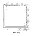
- FIGURES 1 (a) and (b) are block diagrams of exemplary systems according to the presently described embodiments
- FIGURE 2 is a side view of the system of Figure 1(a) according to the presently described embodiments;
- FIGURE 3 is an example infrared image of a polysilicon array showing an active pixel defect
- FIGURE 4 is a graph showing relative resistance from a center of a resistively-coated array being tested to an edge-midpoint and corner thereof.
- the presently described embodiments are directed to a backplane test system using a pressed or deposited resistive film or layer and infra-red (IR) imaging to visualize and quantify the current drive of pixels. It is particularly suited, in one form, for measuring organic light-emitting-diode (OLED) backplanes or other current-actuated-display (CAD) backplanes.
- OLED organic light-emitting-diode
- CAD current-actuated-display
- the presently described embodiments use infra-red imaging to observe heating in a resistive layer applied to a current-driving backplane.
- a functional backplane is completed and the shorting bars are removed, by, for example, parting the substrate, scribing, or other means.
- a resistive coating is applied or pressed, in any of a variety of manners, to the surface of the array.
- flexible contact tapes are pressed onto the row and column electrode pads to make contact with the bus lines.
- a separate contact tape (or other conductive lead material) is also applied to the resistive coating, which may also or alternatively have a guard-ring type electrode to simplify contact.
- the contacts on the tapes are then selectively driven with signals to turn on one or several pixels in any of a variety of known manners.
- the guard-ring electrode is driven to a suitable voltage, possibly ground, and an IR image is taken of the array. Assuming the conductivity of the resistive layer is uniform, the temperature of the resistive layer above a given pixel may be measured for a variety of pixel inputs, including grey scale. The pattern of active pixels may then be varied to test all or a plurality thereof.
- the system 100 includes a backplane 102.
- the backplane 102 may take a variety of forms, such as an OLED backplane or other CAD backplane.
- the backplane has formed thereon column contact pads (such as column pad 104) connected to column bus lines (such as bus line 106).
- the backplane 102 also has row contact pads (such as row contact pad 108) connected to row bus lines (such as bus line 110).
- the circuit may vary by application, however.
- a resistive coating 120 is formed over such circuitry and is provided with a conductive connection, e.g. conductive tape, 122 (in addition to the existing conductive connection of the bus lines and contact pads) to drive the voltage of the coating 120 to a suitable level (e.g. ground).
- a conductive connection e.g. conductive tape
- each column contact pad has connected thereto a conductive connection or lead (such as conductive tape element 130).
- each row contact pad has connected thereto a conductive connection or lead (such as conductive tape element 132).
- the conductive connections or leads are illustrated as conductive tape, but other types of conductive connections may be used.
- the column contact pads and the row contact pads can be selectively driven to various voltage levels using a driver circuit 140 controlled by controller 150.
- controller 150 the connections between the driver 140 and the conductive tape elements that, in one form, connect to the various contact pads, can be accomplished in any of a variety of known manners.
- the driver circuit 140 and controller 150 may take a variety of forms depending on the implementation. These devices may be separate devices, a single device, and/or may be implemented using a variety of hardware configurations and software techniques.
- FIG. 1(b) an alternative system is shown.
- the conductive tape 122 is not used. Rather, a guard ring electrode 124 is shown.
- the guard ring electrode 124 can be driven to a voltage, e.g. ground, during imaging of an array.
- Figure 2 which is a side view of the system shown in Figure 1(a) ), it will be appreciated that the system 100 is further provided with an infrared camera 160 -- as well as a suitable display device 170.
- Figure 2 is a side view of the system 100 and shows the backplane 102, row contact pad 108, row bus line 110 and resistive coating 120. Also shown are the conductive tape element 122 and conductive tape element 132. It should be appreciated that camera and display device are also applicable to the system shown in Figure 1(b) .
- the contact pads can be selectively driven to voltage levels so that individual circuit elements react such that an effect is achieved in the resistive coating.
- the selective actuation of the circuit elements may be based on any of a variety of routines or methods implemented and/or controlled by the driver/controller combination that will allow for a suitable analysis of the resultant data.
- the resistive coating is then imaged by the infrared camera to provide information for analysis of the underlying backplane circuit.
- the analysis may take a variety of forms and may differ as a function of the precise implementation.
- a generated infrared image is displayed on the display device 170 for analysis.
- FIG. 3 An example infrared image is shown in Figure 3 .
- This image 300 of a polysilicon array was taken with an IRRIS-256 IR camera. No resistive layer has been applied-in this case the image is of a short in a very complex, highfrequency-sensor pixel design. Nevertheless, it illustrates the ability of infrared imaging to show fine detail thermometry.
- the resistive layer 120 may be formed in a variety of manners. For example, it may be spun, evaporated, bladed, pressed, or otherwise applied. In one form, its sheet resistivity is compatible with the drive current and voltage of the pixel design and the deposition and removal processes are compatible with subsequent array processing.
- Sample materials include sputtered or solution-deposited particulate ITO, PEDOT, Tungsten, Titanium, and various forms of Carbon.
- ethanol-deposited particulate ITO may produce a sheet resistivity of 10M ⁇ /sq, suitable for a drive transistor that operates at 5V and 20 ⁇ A, and may be removed with ethanol.
- the actual conductivity of the top layer will be a function of geometry, pad resistance, and the resistive layer. Because the top array surface usually consists of passivation and pad metal, a wide variety of resistive film removal methods may be acceptable.
- Rubber material may be used as the resistive layer 120 because it may be rendered conductive by percolation of charge - through conductive particles embedded in the material.
- multi-form carbon is used in silicone rubber, although metal particles may be used as well.
- thin sheets of rubber-laminated substrates may be used as the resistive layer.
- the substrate may be electrically conductive, or the guard ring method may be used.
- IR imaging systems and techniques are available and could be used to improve performance.
- CCD, CMOS, InSb-QW, with various levels of cooling, could be used.
- Sensitivities are down to 60°mK for various devices and high megapixel cameras are available.
- the infrared cameras may be used stroboscopically. This makes sense under pulsed operation to detect peak power, which may be substantially higher than average power. Depending on the thermal conductivity and capacity, pulsed heating and image averaging may produce a superior image.
- guard ring current shunting may be the simplest current return mechanism.
- the resistance at any given pixel will depend on the coordinate of that pixel-those nearest the guard ring will have a lower resistance than in the array center.
- finite-element analysis 400 shown in Figure 4 indicates that the guard ring diameter need be only 20% larger than the array to keep the pixel resistances substantially constant.
- this method may be able to detect linearity, threshold, and saturation effects.
Landscapes
- Engineering & Computer Science (AREA)
- Physics & Mathematics (AREA)
- Computer Hardware Design (AREA)
- General Physics & Mathematics (AREA)
- Theoretical Computer Science (AREA)
- Electroluminescent Light Sources (AREA)
- Control Of Indicators Other Than Cathode Ray Tubes (AREA)
- Control Of El Displays (AREA)
- Testing Electric Properties And Detecting Electric Faults (AREA)
Abstract
Description
- Testing backplanes that drive current rather than voltage presents a challenging problem. At present, there is a need for an acceptable solution for measuring current actuated display (CAD) backplanes prior to application of a display medium to such backplanes.
- Typically, backplanes are fabricated with test structures that allow general parametric measurement of the substrate, without any detail pertaining to individual display elements (pixels, data lines, gate lines, ground busses, power busses). In this regard, with satisfactory substrate parameters, displays are then assembled with a medium (e.g. an organic light emitting diode (OLED)). The finished displays may then be imaged with a camera to measure uniformity, area defects, line defects, and pixel defects. However, with these types of testing systems, problems cannot be detected until after the display is completed.
- A variety of testers for AMLCD backplanes are known. However, none are known for OLED backplanes.
- Also,
U.S. Patent No. 7,295,030 teaches the use of a vacuum tip to capture current without contact. However, a convenient visual system is not disclosed. - In one aspect of the presently described embodiments, the backplane test system comprises conductive connections to circuit elements of the backplane, a drive circuit to selectively drive the circuit elements through the conductive connections, a resistive layer over the backplane to cover the circuit elements, and, an infrared camera to generate an infrared image of the resistive coating while the circuit elements are being driven.
- In another aspect of the presently described embodiments, the conductive connections comprise contact pads connected to circuit elements via bus lines.
- In another aspect of the presently described embodiments, the conductive connections comprise conductive tape elements.
- In another aspect of the presently described embodiments, the resistive layer is applied by one of spinning, evaporation, blading and pressing.
- In another aspect of the presently described embodiments, the resistive layer is comprised of one of indium tin oxide (ITO), PEDOT, tungsten, titanium and carbon.
- In another aspect of the presently described embodiments, the resistive layer is a rubber material.
- In another aspect of the presently described embodiments, the resistive layer is transparent.
- In another aspect of the presently described embodiments, the backplane is used for organic light emitting diode (OLED) applications.
- In another aspect of the presently described embodiments, the infrared imager comprises one of a CCD, CMOS and InSb-QW imagers.
- In another aspect of the presently described embodiments, the method comprises forming a resistive layer on a backplane to cover circuit elements, selectively activating the circuit elements and generating an infrared image of the resistive layer during the selective actuation.
- In another aspect of the presently described embodiments, the forming comprises one of spinning, evaporating, blading and pressing.
- In another aspect of the presently described embodiments, the resistive layer is one of indium tin oxide (ITO), PEDOT, tungsten, titanium and carbon.
- In another aspect of the presently described embodiments, the resistive layer is a rubber material.
- In another aspect of the presently described embodiments, the resistive layer is transparent.
- In another aspect of the presently described embodiments, the backplane is implemented in an organic light emitting diode application.
- In another aspect of the presently described embodiments, the infrared image generating is accomplished by one of a CCD, CMOS or InSb-QW device.
In one embodiment of the method as set forth inclaim 10 the infrared image generating is accomplished by one of a CCD, CMOS or InSb-QW device. -
FIGURES 1 (a) and(b) are block diagrams of exemplary systems according to the presently described embodiments; -
FIGURE 2 is a side view of the system ofFigure 1(a) according to the presently described embodiments; -
FIGURE 3 is an example infrared image of a polysilicon array showing an active pixel defect; and, -
FIGURE 4 is a graph showing relative resistance from a center of a resistively-coated array being tested to an edge-midpoint and corner thereof. - The presently described embodiments are directed to a backplane test system using a pressed or deposited resistive film or layer and infra-red (IR) imaging to visualize and quantify the current drive of pixels. It is particularly suited, in one form, for measuring organic light-emitting-diode (OLED) backplanes or other current-actuated-display (CAD) backplanes.
- The presently described embodiments use infra-red imaging to observe heating in a resistive layer applied to a current-driving backplane. In one form, a functional backplane is completed and the shorting bars are removed, by, for example, parting the substrate, scribing, or other means. A resistive coating is applied or pressed, in any of a variety of manners, to the surface of the array. In one form, flexible contact tapes are pressed onto the row and column electrode pads to make contact with the bus lines. A separate contact tape (or other conductive lead material) is also applied to the resistive coating, which may also or alternatively have a guard-ring type electrode to simplify contact. The contacts on the tapes are then selectively driven with signals to turn on one or several pixels in any of a variety of known manners. In one form, the guard-ring electrode is driven to a suitable voltage, possibly ground, and an IR image is taken of the array. Assuming the conductivity of the resistive layer is uniform, the temperature of the resistive layer above a given pixel may be measured for a variety of pixel inputs, including grey scale. The pattern of active pixels may then be varied to test all or a plurality thereof.
- With reference now to
Figure 1(a) , an example system according to the presently described embodiments is illustrated. In this regard, thesystem 100 includes abackplane 102. As noted above, thebackplane 102 may take a variety of forms, such as an OLED backplane or other CAD backplane. In any case, the backplane has formed thereon column contact pads (such as column pad 104) connected to column bus lines (such as bus line 106). Thebackplane 102 also has row contact pads (such as row contact pad 108) connected to row bus lines (such as bus line 110). The circuit may vary by application, however. - The complete circuitry of the
backplane 102 is not shown for ease of reference. However, according to the presently described embodiments, aresistive coating 120 is formed over such circuitry and is provided with a conductive connection, e.g. conductive tape, 122 (in addition to the existing conductive connection of the bus lines and contact pads) to drive the voltage of thecoating 120 to a suitable level (e.g. ground). Similarly, each column contact pad has connected thereto a conductive connection or lead (such as conductive tape element 130). Likewise, each row contact pad has connected thereto a conductive connection or lead (such as conductive tape element 132). The conductive connections or leads are illustrated as conductive tape, but other types of conductive connections may be used. - With this configuration, the column contact pads and the row contact pads can be selectively driven to various voltage levels using a
driver circuit 140 controlled bycontroller 150. It should be appreciated that, although not shown, the connections between thedriver 140 and the conductive tape elements that, in one form, connect to the various contact pads, can be accomplished in any of a variety of known manners. Also, thedriver circuit 140 andcontroller 150 may take a variety of forms depending on the implementation. These devices may be separate devices, a single device, and/or may be implemented using a variety of hardware configurations and software techniques. - Referring to
Figure 1(b) , an alternative system is shown. In this system, theconductive tape 122 is not used. Rather, aguard ring electrode 124 is shown. Theguard ring electrode 124 can be driven to a voltage, e.g. ground, during imaging of an array. - With reference now to
Figure 2 (which is a side view of the system shown inFigure 1(a) ), it will be appreciated that thesystem 100 is further provided with aninfrared camera 160 -- as well as asuitable display device 170.
Figure 2 is a side view of thesystem 100 and shows thebackplane 102,row contact pad 108,row bus line 110 andresistive coating 120. Also shown are theconductive tape element 122 andconductive tape element 132. It should be appreciated that camera and display device are also applicable to the system shown inFigure 1(b) . - As alluded to above, in operation, after the backplane is coated with the
conductive layer 120, the contact pads can be selectively driven to voltage levels so that individual circuit elements react such that an effect is achieved in the resistive coating. It should be appreciated that the selective actuation of the circuit elements may be based on any of a variety of routines or methods implemented and/or controlled by the driver/controller combination that will allow for a suitable analysis of the resultant data. The resistive coating is then imaged by the infrared camera to provide information for analysis of the underlying backplane circuit. Of course, the analysis may take a variety of forms and may differ as a function of the precise implementation. In one form, a generated infrared image is displayed on thedisplay device 170 for analysis. - An example infrared image is shown in
Figure 3 . Thisimage 300 of a polysilicon array was taken with an IRRIS-256 IR camera. No resistive layer has been applied-in this case the image is of a short in a very complex, highfrequency-sensor pixel design. Nevertheless, it illustrates the ability of infrared imaging to show fine detail thermometry. - The
resistive layer 120 may be formed in a variety of manners. For example, it may be spun, evaporated, bladed, pressed, or otherwise applied. In one form, its sheet resistivity is compatible with the drive current and voltage of the pixel design and the deposition and removal processes are compatible with subsequent array processing. Sample materials include sputtered or solution-deposited particulate ITO, PEDOT, Tungsten, Titanium, and various forms of Carbon. For example, ethanol-deposited particulate ITO may produce a sheet resistivity of 10MΩ/sq, suitable for a drive transistor that operates at 5V and 20µA, and may be removed with ethanol. Because the array will typically have contact pads with lower sheet resistance, the actual conductivity of the top layer will be a function of geometry, pad resistance, and the resistive layer. Because the top array surface usually consists of passivation and pad metal, a wide variety of resistive film removal methods may be acceptable. - Rubber material may be used as the
resistive layer 120 because it may be rendered conductive by percolation of charge - through conductive particles embedded in the material. In one form, multi-form carbon is used in silicone rubber, although metal particles may be used as well. - In this regard, thin sheets of rubber-laminated substrates may be used as the resistive layer. The substrate may be electrically conductive, or the guard ring method may be used.
- One application for current-driver backplanes is for OLEDs, for which stainless steel is often used as a backplane. The thermal conductivity is 16 times higher for stainless than glass, so, depending on the thickness of the buffer layers, there may be a thermal sink to the substrate. This will vary according to specific substrates and designs.
- Three methods may be employed to improve the signal in such cases. First, polymeric materials, which are much less thermally conductive, may be used for the buffer layer. Specific thermal shunt resistance would be analyzed for specific designs. Note that joule heating in the driver transistor itself may have a very different thermal shunt resistance than the applied resistive layer.
- Second, a variety of IR imaging systems and techniques are available and could be used to improve performance. For example, CCD, CMOS, InSb-QW, with various levels of cooling, could be used. Sensitivities are down to 60°mK for various devices and high megapixel cameras are available.
- Third, the infrared cameras may be used stroboscopically. This makes sense under pulsed operation to detect peak power, which may be substantially higher than average power. Depending on the thermal conductivity and capacity, pulsed heating and image averaging may produce a superior image.
- In addition, although a number of approaches may be used (including the
conductive tape 122 ofFigure 1(a) ), guard ring current shunting, as shown inFigure 1(b) , may be the simplest current return mechanism. In this case, the resistance at any given pixel will depend on the coordinate of that pixel-those nearest the guard ring will have a lower resistance than in the array center. However, in at least one form, finite-element analysis 400 shown inFigure 4 indicates that the guard ring diameter need be only 20% larger than the array to keep the pixel resistances substantially constant. InFigure 4 , relative resistance (RELATIVE R (x,y)) for positions X from the center of the array to the edge-midpoint (y=0) (data points shown as squares (B) inFigure 4 ) and from the center of the array to a corner (y=x) (data points shown as circles (C) inFigure 4 ). - Given that pixels may be driven over a variety of gray levels, this method may be able to detect linearity, threshold, and saturation effects.
- It will be appreciated that various of the above-disclosed and other features and functions, or alternatives thereof, may be desirably combined into many other different systems or applications.
Claims (15)
- A system for testing a current actuated display backplane having circuit elements disposed thereon, the system comprising:conductive connections to the circuit elements;a drive circuit to selectively drive the circuit elements through the conductive connections;a resistive layer over the backplane to cover the circuit elements; and,an infrared camera to generate an infrared image of the resistive coating while the circuit elements are being driven.
- The system as set forth in claim 1 wherein the conductive connections comprise contact pads connected to circuit elements via bus lines.
- The system as set forth in claim 2 wherein the conductive connections comprise conductive tape elements.
- The system as set forth in claim 1 wherein the resistive layer is applied by one of spinning, evaporation, blading and pressing.
- The system as set forth in claim 1 wherein the resistive layer is comprised of one of indium tin oxide (ITO), PEDOT, tungsten, titanium and carbon.
- The system as set forth in claim 1 wherein the resistive layer is a rubber material.
- The system as set forth in claim 1 wherein the resistive layer is transparent.
- The system as set forth in claim 1 wherein the backplane is used for organic light emitting diode (OLED) applications.
- The system as set forth in claim 1 wherein the infrared imager comprises one of a CCD, CMOS and InSb-QW imagers.
- A method for testing current actuated display backplanes having circuit elements disposed thereon, the method comprising:forming a resistive layer on the backplane to cover the circuit elements;selectively activating the circuit elements; and,generating an infrared image of the resistive layer during the selective actuation.
- The method as set forth in claim 10 wherein the forming comprises one of spinning, evaporating, blading and pressing.
- The method as set forth in claim 10 wherein the resistive layer is one of indium tin oxide (ITO), PEDOT, tungsten, titanium and carbon.
- The method as set forth in claim 10 wherein the resistive layer is a rubber material.
- The method as set forth in claim 10 wherein the resistive layer is transparent.
- The method as set forth in claim 10 wherein the backplane is implemented in an organic light emitting diode application.
Applications Claiming Priority (1)
| Application Number | Priority Date | Filing Date | Title |
|---|---|---|---|
| US12/408,219 US10186179B2 (en) | 2009-03-20 | 2009-03-20 | Current-actuated-display backplane tester and method |
Publications (2)
| Publication Number | Publication Date |
|---|---|
| EP2230661A2 true EP2230661A2 (en) | 2010-09-22 |
| EP2230661A3 EP2230661A3 (en) | 2011-04-06 |
Family
ID=42224681
Family Applications (1)
| Application Number | Title | Priority Date | Filing Date |
|---|---|---|---|
| EP10156695A Ceased EP2230661A3 (en) | 2009-03-20 | 2010-03-17 | Current-actuated-display backplane tester and method |
Country Status (3)
| Country | Link |
|---|---|
| US (1) | US10186179B2 (en) |
| EP (1) | EP2230661A3 (en) |
| JP (1) | JP5638819B2 (en) |
Families Citing this family (1)
| Publication number | Priority date | Publication date | Assignee | Title |
|---|---|---|---|---|
| CN108538863B (en) * | 2018-05-17 | 2021-09-17 | 京东方科技集团股份有限公司 | Display substrate, repairing method thereof and display device |
Citations (2)
| Publication number | Priority date | Publication date | Assignee | Title |
|---|---|---|---|---|
| US6111424A (en) * | 1997-09-04 | 2000-08-29 | Lucent Technologies Inc. | Testing method and apparatus for flat panel displays using infrared imaging |
| US7295030B2 (en) | 2004-11-08 | 2007-11-13 | International Business Machines Corporation | Thin film transistor tester and corresponding test method |
Family Cites Families (9)
| Publication number | Priority date | Publication date | Assignee | Title |
|---|---|---|---|---|
| US5089700A (en) * | 1990-01-30 | 1992-02-18 | Amdata, Inc. | Apparatus for infrared imaging inspections |
| JP3150324B2 (en) | 1990-07-13 | 2001-03-26 | 株式会社日立製作所 | Method of inspecting thin film transistor substrate and method of repairing wiring of thin film transistor substrate |
| JP3252451B2 (en) * | 1991-07-30 | 2002-02-04 | 株式会社日立製作所 | Thin film transistor liquid crystal substrate inspection method and apparatus |
| KR960002145B1 (en) | 1991-07-30 | 1996-02-13 | 가부시기가이샤 히다찌세이사구쇼 | Detection method of tft lcd panel and the device |
| TW538246B (en) * | 2000-06-05 | 2003-06-21 | Semiconductor Energy Lab | Display panel, display panel inspection method, and display panel manufacturing method |
| US7474115B1 (en) * | 2004-12-28 | 2009-01-06 | Dupont Displays, Inc. | Organic electronic device display defect detection |
| TWI259409B (en) * | 2005-01-07 | 2006-08-01 | Au Optronics Corp | Touch panel for recognizing fingerprint and method of making the same |
| US8067883B2 (en) * | 2008-02-29 | 2011-11-29 | Corning Incorporated | Frit sealing of large device |
| US8536892B2 (en) | 2008-02-29 | 2013-09-17 | Palo Alto Research Center Incorporated | System for testing transistor arrays in production |
-
2009
- 2009-03-20 US US12/408,219 patent/US10186179B2/en active Active
-
2010
- 2010-03-16 JP JP2010058770A patent/JP5638819B2/en not_active Expired - Fee Related
- 2010-03-17 EP EP10156695A patent/EP2230661A3/en not_active Ceased
Patent Citations (2)
| Publication number | Priority date | Publication date | Assignee | Title |
|---|---|---|---|---|
| US6111424A (en) * | 1997-09-04 | 2000-08-29 | Lucent Technologies Inc. | Testing method and apparatus for flat panel displays using infrared imaging |
| US7295030B2 (en) | 2004-11-08 | 2007-11-13 | International Business Machines Corporation | Thin film transistor tester and corresponding test method |
Non-Patent Citations (1)
| Title |
|---|
| MAEDA S ET AL: "PRECISE DETECTION OF SHORT-CIRCUIT DEFECTS ON TFT SUBSTRATE BY INFRARED IMAGE MATCHING", SYSTEMS & COMPUTERS IN JAPAN, WILEY, HOBOKEN, NJ, US, vol. 30, no. 12, 15 November 1999 (1999-11-15), pages 72 - 84, XP000870949, ISSN: 0882-1666, DOI: 10.1002/(SICI)1520-684X(19991115)30:12<72::AID-SCJ8>3.0.CO;2-P * |
Also Published As
| Publication number | Publication date |
|---|---|
| US10186179B2 (en) | 2019-01-22 |
| JP2010225588A (en) | 2010-10-07 |
| US20100237244A1 (en) | 2010-09-23 |
| JP5638819B2 (en) | 2014-12-10 |
| EP2230661A3 (en) | 2011-04-06 |
Similar Documents
| Publication | Publication Date | Title |
|---|---|---|
| US11346729B2 (en) | High resolution pressure sensing | |
| US6859062B2 (en) | Apparatus and method for inspecting a board used in a liquid crystal panel | |
| US10234351B2 (en) | Display substrate and display device, pressure detection system and detection method thereof | |
| US20150056365A1 (en) | Method for inspecting solution discharge apparatus and method for producing device | |
| JP6753615B2 (en) | Distribution measurement sensor, distribution measurement sensor system, distribution measurement program and recording medium | |
| TWI468703B (en) | Wiring testing method, wiring testing device, wiring testing computer program product, and storage medium | |
| US10620064B2 (en) | Pressure sensor | |
| TWI496227B (en) | Method and system for improved testing of transistor arrays | |
| DE112019004840T5 (en) | FINGERPRINT DETECTION DEVICE AND DISPLAY DEVICE WITH FINGERPRINT DETECTION DEVICE | |
| JP4110172B2 (en) | Active matrix panel inspection apparatus, inspection method, and active matrix OLED panel manufacturing method | |
| KR20180015024A (en) | Apparatus and method for testing of touch electrode of on-cell touch organic light-emitting display panel | |
| US10186179B2 (en) | Current-actuated-display backplane tester and method | |
| WO2013073387A1 (en) | Wire inspection method, and wire inspection device | |
| JP2011090358A (en) | Inspection device of capacitive touch panel, and inspection method | |
| TWI908866B (en) | Biometric skin contact sensor and method of operating biometric skin contact sensor | |
| JPWO2011070663A1 (en) | TFT substrate inspection apparatus and TFT substrate inspection method | |
| CN111289381A (en) | Method for detecting bending resistance of screen body | |
| CN114137437A (en) | Method for detecting short circuit of sub-millimeter light-emitting diode backlight substrate circuit | |
| KR102343598B1 (en) | Touch panel and display device comprising the same | |
| JP2011237434A (en) | Calibration method of electronic chip and electronic chip and temperature pattern detector for carrying out the same | |
| KR102932647B1 (en) | Stretchable display devices in which tensile sensors embedded and manufacturing method thereof | |
| US11271016B2 (en) | Array substrate and fabrication method thereof, display apparatus | |
| TW202020415A (en) | Pressure sensor and method for manufacturing pressure sensor | |
| CN203164565U (en) | Thin film transistor array substrate, display panel and display equipment | |
| KR20260017469A (en) | Biometric sensor including oxide semiconductor, biometric sensor on display, and method for manufacturing and using the same |
Legal Events
| Date | Code | Title | Description |
|---|---|---|---|
| PUAI | Public reference made under article 153(3) epc to a published international application that has entered the european phase |
Free format text: ORIGINAL CODE: 0009012 |
|
| AK | Designated contracting states |
Kind code of ref document: A2 Designated state(s): AT BE BG CH CY CZ DE DK EE ES FI FR GB GR HR HU IE IS IT LI LT LU LV MC MK MT NL NO PL PT RO SE SI SK SM TR |
|
| AX | Request for extension of the european patent |
Extension state: AL BA ME RS |
|
| PUAL | Search report despatched |
Free format text: ORIGINAL CODE: 0009013 |
|
| AK | Designated contracting states |
Kind code of ref document: A3 Designated state(s): AT BE BG CH CY CZ DE DK EE ES FI FR GB GR HR HU IE IS IT LI LT LU LV MC MK MT NL NO PL PT RO SE SI SK SM TR |
|
| AX | Request for extension of the european patent |
Extension state: AL BA ME RS |
|
| 17P | Request for examination filed |
Effective date: 20111006 |
|
| 17Q | First examination report despatched |
Effective date: 20170707 |
|
| STAA | Information on the status of an ep patent application or granted ep patent |
Free format text: STATUS: THE APPLICATION HAS BEEN REFUSED |
|
| 18R | Application refused |
Effective date: 20190803 |