EP2226833A1 - Thin film transistor, method of fabricating the same, and organic light emitting diode display device including the same - Google Patents
Thin film transistor, method of fabricating the same, and organic light emitting diode display device including the same Download PDFInfo
- Publication number
- EP2226833A1 EP2226833A1 EP10154686A EP10154686A EP2226833A1 EP 2226833 A1 EP2226833 A1 EP 2226833A1 EP 10154686 A EP10154686 A EP 10154686A EP 10154686 A EP10154686 A EP 10154686A EP 2226833 A1 EP2226833 A1 EP 2226833A1
- Authority
- EP
- European Patent Office
- Prior art keywords
- layer
- forming
- metal catalyst
- silicon layer
- substrate
- Prior art date
- Legal status (The legal status is an assumption and is not a legal conclusion. Google has not performed a legal analysis and makes no representation as to the accuracy of the status listed.)
- Granted
Links
Images


Classifications
-
- H—ELECTRICITY
- H10—SEMICONDUCTOR DEVICES; ELECTRIC SOLID-STATE DEVICES NOT OTHERWISE PROVIDED FOR
- H10D—INORGANIC ELECTRIC SEMICONDUCTOR DEVICES
- H10D30/00—Field-effect transistors [FET]
- H10D30/01—Manufacture or treatment
- H10D30/021—Manufacture or treatment of FETs having insulated gates [IGFET]
- H10D30/031—Manufacture or treatment of FETs having insulated gates [IGFET] of thin-film transistors [TFT]
- H10D30/0312—Manufacture or treatment of FETs having insulated gates [IGFET] of thin-film transistors [TFT] characterised by the gate electrodes
- H10D30/0314—Manufacture or treatment of FETs having insulated gates [IGFET] of thin-film transistors [TFT] characterised by the gate electrodes of lateral top-gate TFTs comprising only a single gate
-
- H—ELECTRICITY
- H10—SEMICONDUCTOR DEVICES; ELECTRIC SOLID-STATE DEVICES NOT OTHERWISE PROVIDED FOR
- H10D—INORGANIC ELECTRIC SEMICONDUCTOR DEVICES
- H10D30/00—Field-effect transistors [FET]
- H10D30/01—Manufacture or treatment
- H10D30/021—Manufacture or treatment of FETs having insulated gates [IGFET]
- H10D30/031—Manufacture or treatment of FETs having insulated gates [IGFET] of thin-film transistors [TFT]
- H10D30/0312—Manufacture or treatment of FETs having insulated gates [IGFET] of thin-film transistors [TFT] characterised by the gate electrodes
- H10D30/0316—Manufacture or treatment of FETs having insulated gates [IGFET] of thin-film transistors [TFT] characterised by the gate electrodes of lateral bottom-gate TFTs comprising only a single gate
-
- H—ELECTRICITY
- H10—SEMICONDUCTOR DEVICES; ELECTRIC SOLID-STATE DEVICES NOT OTHERWISE PROVIDED FOR
- H10D—INORGANIC ELECTRIC SEMICONDUCTOR DEVICES
- H10D30/00—Field-effect transistors [FET]
- H10D30/01—Manufacture or treatment
- H10D30/021—Manufacture or treatment of FETs having insulated gates [IGFET]
- H10D30/031—Manufacture or treatment of FETs having insulated gates [IGFET] of thin-film transistors [TFT]
- H10D30/0321—Manufacture or treatment of FETs having insulated gates [IGFET] of thin-film transistors [TFT] comprising silicon, e.g. amorphous silicon or polysilicon
-
- H—ELECTRICITY
- H10—SEMICONDUCTOR DEVICES; ELECTRIC SOLID-STATE DEVICES NOT OTHERWISE PROVIDED FOR
- H10D—INORGANIC ELECTRIC SEMICONDUCTOR DEVICES
- H10D30/00—Field-effect transistors [FET]
- H10D30/60—Insulated-gate field-effect transistors [IGFET]
- H10D30/67—Thin-film transistors [TFT]
- H10D30/674—Thin-film transistors [TFT] characterised by the active materials
-
- H—ELECTRICITY
- H10—SEMICONDUCTOR DEVICES; ELECTRIC SOLID-STATE DEVICES NOT OTHERWISE PROVIDED FOR
- H10D—INORGANIC ELECTRIC SEMICONDUCTOR DEVICES
- H10D30/00—Field-effect transistors [FET]
- H10D30/60—Insulated-gate field-effect transistors [IGFET]
- H10D30/67—Thin-film transistors [TFT]
- H10D30/6757—Thin-film transistors [TFT] characterised by the structure of the channel, e.g. transverse or longitudinal shape or doping profile
-
- H—ELECTRICITY
- H10—SEMICONDUCTOR DEVICES; ELECTRIC SOLID-STATE DEVICES NOT OTHERWISE PROVIDED FOR
- H10D—INORGANIC ELECTRIC SEMICONDUCTOR DEVICES
- H10D86/00—Integrated devices formed in or on insulating or conducting substrates, e.g. formed in silicon-on-insulator [SOI] substrates or on stainless steel or glass substrates
- H10D86/01—Manufacture or treatment
- H10D86/021—Manufacture or treatment of multiple TFTs
- H10D86/0221—Manufacture or treatment of multiple TFTs comprising manufacture, treatment or patterning of TFT semiconductor bodies
- H10D86/0223—Manufacture or treatment of multiple TFTs comprising manufacture, treatment or patterning of TFT semiconductor bodies comprising crystallisation of amorphous, microcrystalline or polycrystalline semiconductor materials
- H10D86/0225—Manufacture or treatment of multiple TFTs comprising manufacture, treatment or patterning of TFT semiconductor bodies comprising crystallisation of amorphous, microcrystalline or polycrystalline semiconductor materials using crystallisation-promoting species, e.g. using a Ni catalyst
-
- H—ELECTRICITY
- H10—SEMICONDUCTOR DEVICES; ELECTRIC SOLID-STATE DEVICES NOT OTHERWISE PROVIDED FOR
- H10D—INORGANIC ELECTRIC SEMICONDUCTOR DEVICES
- H10D86/00—Integrated devices formed in or on insulating or conducting substrates, e.g. formed in silicon-on-insulator [SOI] substrates or on stainless steel or glass substrates
- H10D86/40—Integrated devices formed in or on insulating or conducting substrates, e.g. formed in silicon-on-insulator [SOI] substrates or on stainless steel or glass substrates characterised by multiple TFTs
-
- H—ELECTRICITY
- H10—SEMICONDUCTOR DEVICES; ELECTRIC SOLID-STATE DEVICES NOT OTHERWISE PROVIDED FOR
- H10P—GENERIC PROCESSES OR APPARATUS FOR THE MANUFACTURE OR TREATMENT OF DEVICES COVERED BY CLASS H10
- H10P14/00—Formation of materials, e.g. in the shape of layers or pillars
- H10P14/20—Formation of materials, e.g. in the shape of layers or pillars of semiconductor materials
- H10P14/29—Formation of materials, e.g. in the shape of layers or pillars of semiconductor materials characterised by the substrates
- H10P14/2901—Materials
- H10P14/2922—Materials being non-crystalline insulating materials, e.g. glass or polymers
-
- H—ELECTRICITY
- H10—SEMICONDUCTOR DEVICES; ELECTRIC SOLID-STATE DEVICES NOT OTHERWISE PROVIDED FOR
- H10P—GENERIC PROCESSES OR APPARATUS FOR THE MANUFACTURE OR TREATMENT OF DEVICES COVERED BY CLASS H10
- H10P14/00—Formation of materials, e.g. in the shape of layers or pillars
- H10P14/20—Formation of materials, e.g. in the shape of layers or pillars of semiconductor materials
- H10P14/32—Formation of materials, e.g. in the shape of layers or pillars of semiconductor materials characterised by intermediate layers between substrates and deposited layers
- H10P14/3202—Materials thereof
- H10P14/3238—Materials thereof being insulating materials
-
- H—ELECTRICITY
- H10—SEMICONDUCTOR DEVICES; ELECTRIC SOLID-STATE DEVICES NOT OTHERWISE PROVIDED FOR
- H10P—GENERIC PROCESSES OR APPARATUS FOR THE MANUFACTURE OR TREATMENT OF DEVICES COVERED BY CLASS H10
- H10P14/00—Formation of materials, e.g. in the shape of layers or pillars
- H10P14/20—Formation of materials, e.g. in the shape of layers or pillars of semiconductor materials
- H10P14/34—Deposited materials, e.g. layers
- H10P14/3402—Deposited materials, e.g. layers characterised by the chemical composition
- H10P14/3404—Deposited materials, e.g. layers characterised by the chemical composition being Group IVA materials
- H10P14/3411—Silicon, silicon germanium or germanium
-
- H—ELECTRICITY
- H10—SEMICONDUCTOR DEVICES; ELECTRIC SOLID-STATE DEVICES NOT OTHERWISE PROVIDED FOR
- H10P—GENERIC PROCESSES OR APPARATUS FOR THE MANUFACTURE OR TREATMENT OF DEVICES COVERED BY CLASS H10
- H10P14/00—Formation of materials, e.g. in the shape of layers or pillars
- H10P14/20—Formation of materials, e.g. in the shape of layers or pillars of semiconductor materials
- H10P14/38—Formation of materials, e.g. in the shape of layers or pillars of semiconductor materials characterised by treatments done after the formation of the materials
- H10P14/3802—Crystallisation or recrystallisation of non-monocrystalline semiconductor materials, e.g. regrowth
-
- H—ELECTRICITY
- H10—SEMICONDUCTOR DEVICES; ELECTRIC SOLID-STATE DEVICES NOT OTHERWISE PROVIDED FOR
- H10P—GENERIC PROCESSES OR APPARATUS FOR THE MANUFACTURE OR TREATMENT OF DEVICES COVERED BY CLASS H10
- H10P14/00—Formation of materials, e.g. in the shape of layers or pillars
- H10P14/20—Formation of materials, e.g. in the shape of layers or pillars of semiconductor materials
- H10P14/38—Formation of materials, e.g. in the shape of layers or pillars of semiconductor materials characterised by treatments done after the formation of the materials
- H10P14/3802—Crystallisation or recrystallisation of non-monocrystalline semiconductor materials, e.g. regrowth
- H10P14/3806—Crystallisation or recrystallisation of non-monocrystalline semiconductor materials, e.g. regrowth using crystallisation-enhancing elements
Definitions
- the metal catalyst layer 140 When the metal catalyst layer 140 is formed with a surface density of less than 10 11 atoms/cm 2 , the number of seeds, which act as nuclei for crystallization, may be too small, and thus it may be difficult to crystallize the amorphous silicon layer into a polycrystalline silicon layer by the SGS crystallization technique. When the metal catalyst layer 140 is formed with a surface density of more than 10 15 atoms/cm 2 , the amount of metal catalyst diffused into the amorphous silicon layer 120 is too large, and thus the grains produced in the polycrystalline silicon layer are smaller in size. Moreover, the amount of metal catalyst remaining in the polycrystalline silicon layer also increases, and thus the characteristics of a semiconductor layer formed by patterning the polycrystalline silicon layer may be poorer.
- a semiconductor layer 440 is formed by patterning the polycrystalline silicon layer 440a. Then, source and drain conductive layers are formed on the semiconductor layer 440 and patterned to form source and drain electrodes 450 and 451.
- the source and drain electrodes 450 and 451 may be formed of one selected from the group consisting of molybdenum (Mo or a molybdenum (Mo) alloy, chromium (Cr), tungsten (W) or a (W) tungsten alloy, molybdenum-tungsten (MoW), aluminum (Al) or an aluminum alloy, aluminum-neodymium (Al-Nd), titanium (Ti), titanium-nitride (TiN), or copper (Cu) or a copper (Cu) alloy,.
Landscapes
- Thin Film Transistor (AREA)
- Recrystallisation Techniques (AREA)
- Electroluminescent Light Sources (AREA)
- Weting (AREA)
- Chemical & Material Sciences (AREA)
- Crystallography & Structural Chemistry (AREA)
Abstract
Description
- Aspects of the present invention relate to a thin film transistor (TFT), a method of fabricating the same, and an organic light emitting diode (OLED) display device including the same. More particularly, aspects of the present invention relate to a TFT, a method of fabricating the same, and an OLED display device including the same, where the fabrication process can remove most of a metal catalyst remaining in a semiconductor layer formed from a polycrystalline silicon layer crystallized using the metal catalyst by gettering using a metal etchant.
- Thin film transistors (TFTs) have been typically used as active elements of active matrix liquid crystal display (AMLCD) devices, and switching and driving elements of organic light emitting diode (OLED) display devices. In these cases, it is necessary to control the characteristics of the TFTs according to the required characteristics of the elements of the particular devices. One of the important factors which determine the characteristics of the TFTs is leakage current.
- In general, in a TFT having a semiconductor layer formed of a polycrystalline silicon layer which is crystallized by a crystallization method that does not use a metal catalyst, the leakage current tends to increase when the width of a channel region increases and tends to decrease when the length of the channel region increases. However, even though the length of the channel region is increased in order to reduce the leakage current, the effect is minor. Moreover, in a display device, if the length of the channel region is increased, the size of the entire device is also increased, and the aperture ratio is reduced. Thus, the length of the channel region is limited.
- Recently, methods of crystallizing an amorphous silicon layer using a metal catalyst have been extensively studied, since the methods have advantages in that the crystallization can be achieved at a lower temperature over a shorter crystallization time than in a solid phase crystallization (SPC) method. Also, a broader range of process conditions can be used and the reproducibility is higher than in an excimer laser crystallization (ELC) method. However, in a TFT using a polycrystalline silicon layer that has been crystallized using a metal catalyst as a semiconductor layer, the leakage current of the TFT as a function of changes in the length or width of the channel region changes without a clear tendency, unlike the tendency that other TFTs demonstrate. Accordingly, a TFT having a semiconductor layer formed of a polycrystalline silicon layer crystallized using a metal catalyst has problems in that the leakage current as a function of the size of the channel region of the semiconductor layer cannot be estimated, and the size of the channel region of the semiconductor layer, which will be used to control the leakage current, cannot be determined.
- Aspects of the present invention provide a thin film transistor (TFT), a method of fabricating the same, and an organic light emitting diode (OLED) display device including the same, where the fabrication process can remove most of a metal catalyst remaining in a semiconductor layer formed of a polycrystalline silicon layer crystallized using the metal catalyst by gettering using a metal etchant, thus improving the characteristics of the TFT.
- According to an exemplary embodiment of the present invention, a TFT includes: a substrate; a buffer layer disposed on the substrate; a semiconductor layer disposed on the buffer layer; a gate electrode insulated from the semiconductor layer; a gate insulating layer insulating the semiconductor layer from the gate electrode; and source and drain electrodes insulated from the gate electrode and partially connected to the semiconductor layer, wherein the semiconductor layer comprises at least one groove.
- According to another exemplary embodiment of the present invention, an OLED display device includes: a substrate; a buffer layer disposed on the substrate; a semiconductor layer disposed on the buffer layer; a gate electrode insulated from the semiconductor layer; a gate insulating layer insulating the semiconductor layer from the gate electrode; source and drain electrodes insulated from the gate electrode and partially connected to the semiconductor layer; an insulating layer disposed on the entire surface of the substrate; a first electrode disposed on the insulating layer and electrically connected to one of the source and drain electrodes; an organic layer; and a second electrode, wherein the semiconductor layer comprises at least one groove.
- Additional aspects and/or advantages of the invention will be set forth in part in the description which follows and, in part, will be obvious from the description, or may be learned by practice of the invention.
- These and/or other aspects and advantages of the invention will become apparent and more readily appreciated from the following description of the embodiments, taken in conjunction with the accompanying drawings of which:
-
FIGs. 1A to 1D are cross-sectional views illustrating a crystallization process for a polycrystalline silicon layer according to an exemplary embodiment of the present invention; -
FIGs. 2A and 2B are cross-sectional views illustrating gettering on a polycrystalline silicon layer according to another exemplary embodiment of the present invention; -
FIG. 2C is a photograph of the surface of a polycrystalline silicon layer taken after gettering according to the embodiment ofFIGs. 2A and 2B ; -
FIGs. 2D to 2F are graphs of metal catalyst concentrations of polycrystalline silicon layers to which gettering has been applied, according to the embodiment ofFIGs. 2A and 2B ; -
FIGs. 3A to 3C are cross-sectional views illustrating a process of fabricating a top-gate TFT according to another exemplary embodiment of the present invention; -
FIGs. 4A to 4C are cross-sectional views illustrating a process of fabricating a bottom-gate TFT according to another exemplary embodiment of the present invention; and -
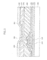
FIG. 5 is a cross-sectional view of an OLED display device according to another exemplary embodiment of the present invention. - Reference will now be made in detail to the present embodiments of the present invention, examples of which are illustrated in the accompanying drawings, wherein like reference numerals refer to the like elements throughout. The embodiments are described below in order to explain the present invention by referring to the figures.
-
FIGs. 1A to 1D are cross-sectional views illustrating a crystallization process for a polycrystalline silicon layer according to an exemplary embodiment of the present invention. First, as illustrated inFIG. 1A , abuffer layer 110 is formed on asubstrate 100 that is formed of glass or plastic. Thebuffer layer 110 is an insulating layer and may be formed of a silicon dioxide layer, a silicon nitride layer, or a combination thereof, by chemical vapor deposition (CVD) or physical vapor deposition (PVD). Thebuffer layer 110 serves to prevent diffusion of moisture or impurities generated in thesubstrate 100 and to adjust the heat transfer rate during crystallization, thereby facilitating crystallization of an amorphous silicon layer. However, thebuffer layer 110 is not required in all aspects of the present invention. - Subsequently, an
amorphous silicon layer 120 is formed on thebuffer layer 110. Theamorphous silicon layer 120 may be deposited by CVD or PVD. During or after the formation of theamorphous silicon layer 120, a dehydrogenation process may be performed to reduce the concentration of hydrogen. - Then, the
amorphous silicon layer 120 is crystallized into a polycrystalline silicon layer. According to aspects of the present invention, the amorphous silicon layer is crystallized into a polycrystalline silicon layer by a crystallization method using a metal catalyst, such as a metal induced crystallization (MIC) technique, a metal induced lateral crystallization (MILC) technique, or a super grain silicon (SGS) technique. However, the crystallization techniques are not limited thereto. - The SGS technique is a method of crystallizing an
amorphous silicon layer 120 in which the concentration of the metal catalyst diffused into theamorphous silicon layer 120 is lowered in order to control the grain size of the polycrystalline silicon to be within the range of several µm to several hundreds of µm. To lower the concentration of the metal catalyst diffused into theamorphous silicon layer 120, a diffusion layer 130 (seeFIG. 1B ) may be formed on theamorphous silicon layer 120, and a metal catalyst layer 140 (seeFIG. 1B ) may be formed on thediffusion layer 130 and annealed to diffuse the metal catalyst into theamorphous silicon layer 120. Alternatively, the concentration of the metal catalyst diffused in theamorphous silicon layer 120 may be lowered by forming themetal catalyst layer 140 at a low concentration without forming the diffusion layer on theamorphous silicon layer 120. - In an exemplary embodiment of the present invention, the polycrystalline silicon layer may be formed by an SGS crystallization technique, which will now be described.
FIG. 1B is a cross-sectional view illustrating a process of forming adiffusion layer 130 and ametal catalyst layer 140 on theamorphous silicon layer 120. Thediffusion layer 130 is formed on theamorphous silicon layer 120. Thediffusion layer 130 may be formed of a silicon nitride layer or a silicon dioxide layer, into which a metal catalyst formed in the following process may diffuse through annealing, and may be formed in a double-layered structure of the silicon nitride layer and the silicon dioxide layer. Moreover, in the case where thediffusion layer 130 is formed in the double-layered structure, any one of the layers may be patterned to adjust the position where the metal catalyst is diffused. Thediffusion layer 130 may be formed by any suitable deposition method such as, for example, CVD or PVD. - In the example shown, the
diffusion layer 130 may be formed to a thickness of 1 through 2,000 Å. When the thickness of thediffusion layer 130 is less than 1 Å, it may be difficult to control the amount of metal catalyst that diffuses through thediffusion layer 130. When the thickness of thediffusion layer 130 is more than 2,000 Å, the amount of metal catalyst diffused into theamorphous silicon layer 120 may be too small, and thus it is difficult to crystallize theamorphous silicon layer 120 into a polycrystalline silicon layer. - Subsequently, a metal catalyst is deposited on the
diffusion layer 130 to form ametal catalyst layer 140. The metal catalyst may be selected from the group consisting of nickel (Ni), palladium (Pd), silver (Ag), gold (Au), aluminum (Al), tin (Sn), antimony (Sb), copper (Cu), terbium (Tb), and cadmium (Cd), and preferably the metal catalyst may be Ni. Themetal catalyst layer 140 may be formed to have a surface density of 1011 through 1015 atoms/cm2 on thediffusion layer 130. When themetal catalyst layer 140 is formed with a surface density of less than 1011 atoms/cm2, the number of seeds, which act as nuclei for crystallization, may be too small, and thus it may be difficult to crystallize the amorphous silicon layer into a polycrystalline silicon layer by the SGS crystallization technique. When themetal catalyst layer 140 is formed with a surface density of more than 1015 atoms/cm2, the amount of metal catalyst diffused into theamorphous silicon layer 120 is too large, and thus the grains produced in the polycrystalline silicon layer are smaller in size. Moreover, the amount of metal catalyst remaining in the polycrystalline silicon layer also increases, and thus the characteristics of a semiconductor layer formed by patterning the polycrystalline silicon layer may be poorer. -
FIG. 1C is a cross-sectional view illustrating a process of diffusing the metal catalyst through thediffusion layer 130 to an interface of theamorphous silicon layer 120 by annealing thesubstrate 110. Referring toFIG. 1C , thesubstrate 100, on which thebuffer layer 110, theamorphous silicon layer 120, thediffusion layer 130, and themetal catalyst layer 140 are formed, is annealed to move some of the metal catalyst of themetal catalyst layer 140 to the surface of theamorphous silicon layer 120. That is, only a very small amount of metal catalyst 140b from themetal catalyst layer 140 diffuses through thediffusion layer 130 to the surface of theamorphous silicon layer 120 during the annealing, and most of the metal catalyst 140a does not reach theamorphous silicon layer 120, or does not pass at all through thediffusion layer 130. Thus, the amount of metal catalyst 140b reaching the surface of theamorphous silicon layer 120 is determined by the diffusion blocking ability of thediffusion layer 130, which is closely related to the thickness of thediffusion layer 130. That is, as the thickness of thediffusion layer 130 increases, the diffused amount of the metal catalyst 140b decreases, and thus the produced grains become larger. On the other hand, if the thickness of thediffusion layer 130 decreases, the diffused amount of the metal catalyst 140b increases, and thus the produced grains become smaller. - The annealing process may be performed at a temperature of about 200 to about 900 °C, preferably at a temperature of about 350 to about 500 °C for several seconds to several hours to diffuse the metal catalyst. Under the annealing conditions described above, it is possible to prevent deformation of the
substrate 100 caused by excessive annealing, and to lower production costs and increase yield. The annealing process may be one of a furnace process, a rapid thermal annealing (RTA) process, a UV process, and a laser process. -
FIG. 1D is a cross-sectional view illustrating a process of crystallizing theamorphous silicon layer 120 into apolycrystalline silicon layer 160 by using the diffused metal catalyst. Referring toFIG. 1D , theamorphous silicon layer 120 is crystallized into apolycrystalline silicon layer 160 by the metal catalysts 140b that have diffused to the surface of theamorphous silicon layer 120 through thediffusion layer 130. That is, the diffused metal catalyst 140b is bonded to silicon of theamorphous silicon layer 120 to form metal silicides, which form seeds, i.e., nuclei for crystallization, and thus theamorphous silicon layer 120 is crystallized into thepolycrystalline silicon layer 160. - As illustrated in
FIG. 1D , the annealing process is performed without removing thediffusion layer 130 and themetal catalyst layer 140. Alternatively, the polycrystalline silicon layer may be formed by diffusing the metal catalyst 140b onto theamorphous silicon layer 120 to form metal silicides, which are nuclei for crystallization, removing thediffusion layer 130 and themetal catalyst layer 140, and then annealing the baredamorphous silicon layer 120. -
FIGs. 2A and 2B are cross-sectional views illustrating gettering on a polycrystalline silicon layer according to another exemplary embodiment of the present invention. First, as illustrated inFIG. 2A , a buffer layer 210 and apolycrystalline silicon layer 220 crystallized using the metal catalyst according toFIGs. 1A through 1D have been formed on a substrate 200. Here, the exemplary gettering that follows is performed on the substrate 200, from which thediffusion layer 130 and themetal catalyst layer 140 illustrated inFIG. 1D have been deleted fromFIGs. 2A and 2B for purposes of explanation. - The
polycrystalline silicon layer 220 contains residual metal catalysts 140a and 140b, and the concentration of the residual metal catalysts 140a and 140b after the crystallization is about 1×10¹³ to 5×10¹⁴ atoms/cm2. Thepolycrystalline silicon layer 220 is etched with an etchant. - The etchant used is to remove nickel or nickel silicide and includes a mixture of 25% hydrochloric acid (HCl), 10% acetic acid (CH3COOH), and ferric chloride at various concentrations. Moreover, buffered oxide etch (BOE) such as HF or NH4F may be used. When the etchant is used to etch the
polycrystalline silicon layer 220 for about 2 minutes, the residual metal catalysts are dissolved in the etchant, thus allowing the gettering process to proceed. - Referring to
FIG. 2B , when the substrate 200 on which thepolycrystalline silicon layer 220 has been formed is etched, the residual metal catalysts 140a and 140b present in thepolycrystalline silicon layer 220 are removed. Especially, the metal silicide 140a at the grain interface is dissolved in the etchant and removed, and thus grooves or indentations "a" are formed. The formed indentations "a" have various sizes according to the initial concentration of the metal catalyst and the temperature and time of the crystallization annealing process. The indentations "a" may have sizes in the range of about 200 to about 1,000 nm, and fine holes may be formed. -
FIG. 2C is a photograph of the surface of thepolycrystalline silicon layer 220 taken after gettering with the etchant as illustrated inFIG. 2B , from which it can be seen that the indentations "a" are formed after the aggregated metal catalyst and metal silicide 140a are removed. -
FIGs. 2D to 2F are graphs of metal catalyst concentrations of the polycrystalline silicon layers to which gettering has been applied, in which the crystallization is performed using nickel as the metal catalyst.FIG. 2D shows the concentration of nickel catalyst of the polycrystalline silicon layer measured before gettering,FIG. 2E shows the concentration of nickel catalyst of the polycrystalline silicon layer measured after gettering for 1 minute, andFIG. 2F shows the concentration of nickel catalyst of the polycrystalline silicon layer measured after gettering for 2 minutes. - Referring to
FIGs. 2D to 2F , when comparing the amounts of nickel catalyst before and after gettering for 1 and 2 minutes, it can be seen that the amount of nickel catalyst on the surface of the polycrystalline silicon layer is reduced after gettering has been applied for 1 minute (B) and the amount of nickel catalyst is also reduced after gettering has been applied for 2 minutes (C). - Although the grooves are formed on the surface of the polycrystalline silicon layer after gettering, the grooves have no significant effect on the characteristics of a semiconductor layer formed from the polycrystalline silicon layer.
- Table 1 shows the characteristics of the semiconductor layer formed from the
polycrystalline silicon layer 160 after gettering.Table 1 Number of
indentationsThreshold voltage (Vth)(V) Off-current (loff)(A/µm) 4 2.01 2x10-11 6 1.99 1x10-11 8 1.98 1x10-11 - It can be seen from Table 1 that although the indentations "a" are present on the surface of the polycrystalline silicon layer, the threshold voltage (Vth) characteristics and the off-current (loff) characteristics are excellent. Thus, it is possible to effectively remove the metal catalyst by the above-described gettering.
-
FIGs. 3A to 3C are cross-sectional views illustrating a process of fabricating a top-gate TFT according to another exemplary embodiment of the present invention using the process of fabricating the polycrystalline silicon layer. Referring toFIG. 3A , abuffer layer 310 may be formed on asubstrate 300 that is formed of glass, stainless steel, or plastic. Thebuffer layer 310 is an insulating layer and may be formed of a silicon dioxide layer, a silicon nitride layer, or a combination thereof. Thebuffer layer 310 serves to prevent diffusion of moisture or impurities generated in thesubstrate 300 and to adjust the heat transfer rate during crystallization, thereby facilitating crystallization of an amorphous silicon layer. - Subsequently, to form a polycrystalline silicon layer 320a, an amorphous silicon layer is formed on the
buffer layer 310. In the same manner as the exemplary embodiment ofFIGS. 1A to 1D , the amorphous silicon layer is crystallized into a polycrystalline silicon layer 320a using a metal catalyst. Then, the polycrystalline silicon layer 320a is subjected to the above-described gettering ofFIGs. 2A and 2B using a metal etchant to remove residual metal catalysts, thereby forming a polycrystalline silicon layer 320a having indentations "a" formed with the metal catalyst. - Referring to
FIG. 3B , asemiconductor layer 320 is formed on thebuffer layer 310 by patterning the polycrystalline silicon layer 320a. Then, agate insulating layer 330 is formed on the entire surface of thesubstrate 300 including thesemiconductor layer 320. Thegate insulating layer 330 may be a silicon dioxide layer, a silicon nitride layer, or a combination thereof. - Subsequently, a metal layer for a gate electrode (not shown) is formed on the
gate insulating layer 330 using a single layer of aluminum (Al) or an Al alloy such as aluminum-neodymium (Al-Nd), or a multi-layer having an Al alloy stacked on a chrome (Cr) or molybdenum (Mo) alloy, and agate electrode 340 is formed to correspond to a channel region of thesemiconductor layer 320 by etching the metal layer for a gate electrode using a photolithography process. - Then, referring to
FIG. 3C , an interlayer insulating layer 350 is formed on the entire surface of thesubstrate 300 including thegate electrode 340. Here, the interlayer insulating layer 350 may be formed of a silicon dioxide layer, a silicon nitride layer, or a combination thereof. - Next, the interlayer insulating layer 350 and the
gate insulating layer 330 are etched to form contact holes exposing source and drain regions of thesemiconductor layer 320. Source anddrain electrodes 360 and 361 connected to the source and drain regions through the contact holes are formed. In this case, the source and drainelectrodes 360 and 361 may be formed of one selected from the group consisting of molybdenum (Mo) or a molybdenum (Mo) alloy, chromium (Cr), tungsten (W) or a (W) tungsten alloy, molybdenum-tungsten (MoW), aluminum (Al) or an aluminum alloy, aluminum-neodymium (Al-Nd), titanium (Ti), titanium-nitride (TiN), or copper (Cu) or a copper (Cu) alloy,. Further examples include an alloy of molybdenum-tungsten (MoW), an alloy of aluminum-neodymium (AlNd), or titanium-nitride (TiN). Thus, a TFT including thesemiconductor layer 320, thegate electrode 340, and the source and drainelectrodes 360 and 361 is completed. -
FIGs. 4A to 4C are cross-sectional views illustrating a process of fabricating a bottom-gate TFT according to another exemplary embodiment of the present invention using the process of fabricating the polycrystalline silicon layer. Except for particular descriptions below, the process will be described with reference to the descriptions in the above exemplary embodiment. - Referring to
FIG. 4A , abuffer layer 410 is formed on asubstrate 400. To form agate electrode 420, a metal layer is formed on thebuffer layer 410, and agate electrode 420 is formed by etching the metal layer for a gate electrode using a photolithography process. Then, agate insulating layer 430 is formed on thesubstrate 400 including thegate electrode 420. - Subsequently, referring to
FIG. 4B , an amorphous silicon layer is formed on thegate insulating layer 430 and then crystallized into a polycrystalline silicon layer 440a using a metal catalyst in the same manner as the exemplary embodiment ofFIGS. 1A through 1D . The polycrystalline silicon layer 440a is subjected to the gettering described in the exemplary embodiment ofFIGs. 2A and 2B such that the metal catalyst in the polycrystalline silicon layer 440a is removed by the gettering, and thus grooves or indentations "a" remain. - Referring to
FIG. 4C , asemiconductor layer 440 is formed by patterning the polycrystalline silicon layer 440a. Then, source and drain conductive layers are formed on thesemiconductor layer 440 and patterned to form source and drainelectrodes electrodes semiconductor layer 440, thegate electrode 420, and the source and drainelectrodes -
FIG. 5 is a cross-sectional view of an OLED display device including a top-gate TFT according to another exemplary embodiment of the present invention. Referring toFIG. 5 , an insulating layer 365 is formed on the entire surface of thesubstrate 300 including the TFT according to the exemplary embodiment ofFIGS. 3A to 3C . The insulating layer 365 may be an inorganic layer formed of a material selected from the group consisting of silicon dioxide, silicon nitride, and silicate on glass, or an organic layer formed of a polymer selected from the group consisting of a polyimide, a poly(benzocyclobutene), and a polyacrylate. Also, the insulating layer 365 may be formed by stacking the inorganic layer and the organic layer. - A via hole exposing the source or
drain electrode 360 or 361 is formed by etching the insulating layer 365. Afirst electrode 370 connected to one of the source and drainelectrodes 360 and 361 through the via hole is formed. Thefirst electrode 370 may be an anode or a cathode. When thefirst electrode 370 is an anode, the anode may be formed of a transparent conductive layer formed of ITO, IZO, or ITZO, and when thefirst electrode 370 is a cathode, the cathode may be formed of Mg, Ca, Al, Ag, Ba, or an alloy thereof. - Subsequently, a pixel defining layer 375 having an opening that partially exposes the surface of the
first electrode 370 is formed on thefirst electrode 370, and an organic layer 380 including an emission layer is formed on the exposedfirst electrode 370. The organic layer 380 may further include at least one of a hole injection layer, a hole transport layer, a hole blocking layer, an electron blocking layer, an electron injection layer, and an electron transport layer. Then, a second electrode 385 is formed on the organic layer 380. Thus, an OLED display device according to the exemplary embodiment of the present invention is completed. - According to aspects of the present invention as described above, it is possible to remove most of a metal catalyst remaining in a semiconductor layer formed from a polycrystalline silicon layer crystallized using the metal catalyst by gettering using a metal etchant, and thus a TFT having excellent electrical characteristics, a method of fabricating the same, and an OLED display device including the same may be provided.
- Although a few exemplary embodiments of the present invention have been shown and described, it would be appreciated by those skilled in the art that changes may be made in this exemplary embodiment without departing from the principles and spirit of the invention, the scope of which is defined in the claims and their equivalents.
Claims (20)
- A thin film transistor comprising:a buffer layer (310, 410) disposed on a substrate (300, 400);a semiconductor layer (320, 440) disposed on the buffer layer (310, 410);a gate electrode (340, 420) insulated from the semiconductor layer (320, 440);a gate insulating layer (330, 430) insulating the semiconductor layer (320, 440) from the gate electrode (340, 420); andsource (360, 450) and drain (361, 451) electrodes insulated from the gate electrode (340, 420) and partially connected to the semiconductor layer (320, 440),wherein the semiconductor layer (320, 440) comprises at least one indentation (a).
- The thin film transistor of claim 1, wherein the semiconductor layer (320, 440) comprises a metal catalyst (140a, 140b).
- The thin film transistor of claim 1 or 2, wherein each indentation (a) has a size of about 200 to about 1,000 µm.
- The thin film transistor of one of claims 1 to 3, wherein the thin film transistor comprises:a buffer layer (310) disposed on a substrate (300);a semiconductor layer (320) disposed on the buffer layer (310);a gate insulating layer (330) disposed on the semiconductor layer (320);a gate electrode (340) disposed on the gate insulating layer (330) and corresponding to the semiconductor layer (320);an interlayer insulating layer (350) disposed on the entire surface of the substrate (300); andsource (360) and drain (361) electrodes disposed on the interlayer insulating layer (350) and partially connected to the semiconductor layer (320).
- The transistor of one of claims 1 to 3, wherein the thin film transistor comprises:a buffer layer (410) disposed on a substrate (400);a gate electrode (420) disposed on the buffer layer (410);a gate insulating layer (430) disposed on the entire surface of the substrate (400);a semiconductor layer (440) disposed on the gate insulating layer (430) and corresponding to the gate electrode (420) ; andsource (450) and drain (451) electrodes exposing a portion of the semiconductor layer (440) and connected to the semiconductor layer (440).
- The thin film transistor of one of claims 1 to 5, wherein the semiconductor layer is manufactured by:forming a buffer layer on a substrate,forming an amorphous silicon layer on the buffer layer,forming a metal catalyst layer on the amorphous silicon layer,crystallizing the amorphous silicon layer into a polycrystalline silicon layer by annealing the substrate,removing the metal catalyst layer, andetching the polycrystalline silicon layer using an etchant.
- The thin film transistor of claim 6, wherein the crystallization is performed after forming a diffusion layer between the amorphous silicon layer and the metal catalyst layer.
- A method of fabricating a thin film transistor, comprising:forming a buffer layer on a substrate;forming an amorphous silicon layer on the buffer layer;forming a metal catalyst layer on the amorphous silicon layer;crystallizing the amorphous silicon layer into a polycrystalline silicon layer by annealing the substrate;removing the metal catalyst layer;etching the polycrystalline silicon layer using an etchant;forming a semiconductor layer by patterning the polycrystalline silicon layer;forming a gate insulating layer on the semiconductor layer;forming a gate electrode on the gate insulating layer;forming an interlayer insulating layer on the entire surface of the substrate; andforming source and drain electrodes on the interlayer insulating layer to be partially connected to the semiconductor layer.
- A method of fabricating a thin film transistor, comprising:forming a buffer layer on a substrate;forming a gate electrode on the buffer layer;forming a gate insulating layer on the entire surface of the substrate;forming an amorphous silicon layer on the gate insulating layer;forming a metal catalyst layer on the amorphous silicon layer;crystallizing the amorphous silicon layer into a polycrystalline silicon layer by annealing the substrate;removing the metal catalyst layer;etching the polycrystalline silicon layer using an etchant;forming a semiconductor layer corresponding to the gate electrode by patterning the polycrystalline silicon layer; andforming source and drain electrodes exposing a portion of the semiconductor layer and connected to the semiconductor layer.
- The method of claim 8 or 9, wherein the etchant is at least one material selected from the group consisting of hydrochloric acid, acetic acid, ferric chloride, and buffered oxide etch.
- The method of one of claims 8 to 10, wherein the crystallization is performed after forming a diffusion layer between the amorphous silicon layer and the metal catalyst layer.
- The method of one of claims 8 to 11, wherein the metal catalyst layer is formed of a metal selected from the group consisting of nickel (Ni), palladium (Pd), silver (Ag), gold (Au), aluminum (Al), tin (Sn), antimony (Sb), copper (Cu), terbium (Tb), and cadmium (Cd).
- The method of one of claims 8 to 12, wherein the annealing is performed at a temperature of about 350 to about 500 °C.
- The method of one of claims 8 to 13, wherein the residual metal catalyst after crystallization has a concentration of about 1 x 10¹³ to 5 x 10¹⁴ atoms/cm2.
- The method of claim 10, wherein the buffered oxide etch is a mixture of HF and NH4F.
- The method of claim 11, wherein the thickness of the diffusion layer is 1 through 2000 Å.
- An organic light emitting diode (OLED) display device comprising a thin film transistor of one of claims 1 to 7
- A method of manufacturing a semiconductor layer comprising:forming a buffer layer on a substrate,forming an amorphous silicon layer on the buffer layer,forming a metal catalyst layer on the amorphous silicon layer,crystallizing the amorphous silicon layer into a polycrystalline silicon layer by annealing the substrate,removing the metal catalyst layer, andetching the polycrystalline silicon layer using an etchant.
- The method of claim 18, wherein the semiconductor layer comprises at least one indentation, and each indentation has a size of about 200 to about 1,000 µm.
- The method of claim 18 or 19, wherein a diffusion layer is disposed between the amorphous silicon layer and the metal catalyst layer before crystallization.
Applications Claiming Priority (1)
| Application Number | Priority Date | Filing Date | Title |
|---|---|---|---|
| KR1020090018201A KR101015849B1 (en) | 2009-03-03 | 2009-03-03 | Thin film transistor, manufacturing method thereof and organic light emitting display device comprising same |
Publications (2)
| Publication Number | Publication Date |
|---|---|
| EP2226833A1 true EP2226833A1 (en) | 2010-09-08 |
| EP2226833B1 EP2226833B1 (en) | 2013-04-10 |
Family
ID=42102476
Family Applications (1)
| Application Number | Title | Priority Date | Filing Date |
|---|---|---|---|
| EP10154686.9A Not-in-force EP2226833B1 (en) | 2009-03-03 | 2010-02-25 | Method of fabricating a thin film transistor |
Country Status (5)
| Country | Link |
|---|---|
| US (2) | US20100224883A1 (en) |
| EP (1) | EP2226833B1 (en) |
| JP (1) | JP5355450B2 (en) |
| KR (1) | KR101015849B1 (en) |
| CN (1) | CN101826556B (en) |
Cited By (5)
| Publication number | Priority date | Publication date | Assignee | Title |
|---|---|---|---|---|
| EP2323159A1 (en) * | 2009-11-13 | 2011-05-18 | Samsung Mobile Display Co., Ltd. | Method of forming polycrystalline silicon layer, thin film transistor, organic light emitting diode display device having the same, and methods of fabricating the same |
| US8048783B2 (en) | 2009-03-05 | 2011-11-01 | Samsung Mobile Display Co., Ltd. | Method of forming polycrystalline silicon layer and atomic layer deposition apparatus used for the same |
| US8409887B2 (en) | 2009-03-03 | 2013-04-02 | Samsung Display Co., Ltd. | Organic light emitting diode display device and method of fabricating the same |
| US9117798B2 (en) | 2009-03-27 | 2015-08-25 | Samsung Display Co., Ltd. | Thin film transistor, method of fabricating the same and organic light emitting diode display device including the same |
| TWI682523B (en) * | 2019-01-22 | 2020-01-11 | 大陸商深圳市柔宇科技有限公司 | Array substrate and oled display device |
Families Citing this family (8)
| Publication number | Priority date | Publication date | Assignee | Title |
|---|---|---|---|---|
| KR20120131753A (en) * | 2011-05-26 | 2012-12-05 | 삼성디스플레이 주식회사 | Thin film transistor, method of manufacturing thin film transistor, and organic light emitting diode display |
| KR101809661B1 (en) * | 2011-06-03 | 2017-12-18 | 삼성디스플레이 주식회사 | Thin film transistor, manufacturing method of thin film transistor, and organic light emitting diode display including the same |
| CN102651401B (en) * | 2011-12-31 | 2015-03-18 | 京东方科技集团股份有限公司 | A kind of thin film transistor, array substrate and its manufacturing method and display device |
| KR101949861B1 (en) | 2012-10-10 | 2019-02-20 | 삼성디스플레이 주식회사 | Organic light emitting diode display and method for manufacturing organic light emitting diode display |
| CN104240633B (en) * | 2013-06-07 | 2018-01-09 | 上海和辉光电有限公司 | Thin film transistor (TFT) and active matrix organic light-emitting diode component and its manufacture method |
| KR102301501B1 (en) * | 2015-01-21 | 2021-09-13 | 삼성디스플레이 주식회사 | Manufacturing method of flexible display device |
| CN104570515A (en) * | 2015-01-26 | 2015-04-29 | 京东方科技集团股份有限公司 | Array substrate and manufacture method thereof, display panel and display device |
| CN108550583B (en) * | 2018-05-09 | 2021-03-23 | 京东方科技集团股份有限公司 | Display substrate, display device and manufacturing method of display substrate |
Citations (5)
| Publication number | Priority date | Publication date | Assignee | Title |
|---|---|---|---|---|
| US5814540A (en) | 1993-03-05 | 1998-09-29 | Semiconductor Energy Laboratory Co., Ltd. | Method for producing a transistor |
| US20050023531A1 (en) | 2003-07-31 | 2005-02-03 | Semiconductor Energy Laboratory Co., Ltd. | Semiconductor device and method for manufacturing semiconductor device |
| US20060033106A1 (en) | 2004-08-13 | 2006-02-16 | Jin-Wook Seo | Thin film transistor and method of fabricating the same |
| US20060263957A1 (en) * | 2005-04-28 | 2006-11-23 | The Hong Kong University Of Science And Technology | Metal-induced crystallization of amorphous silicon, polycrystalline silicon thin films produced thereby and thin film transistors produced therefrom |
| US20080157083A1 (en) | 2006-12-29 | 2008-07-03 | Samsung Sdi Co., Ltd. | Transistor, fabricating method thereof and flat panel display therewith |
Family Cites Families (35)
| Publication number | Priority date | Publication date | Assignee | Title |
|---|---|---|---|---|
| EP0589049B1 (en) * | 1992-03-25 | 2000-01-12 | Kanegafuchi Chemical Industry Co., Ltd. | Thin polysilicon film and production thereof |
| JPH0669515A (en) * | 1992-08-19 | 1994-03-11 | Fujitsu Ltd | Semiconductor memory device |
| KR100294026B1 (en) * | 1993-06-24 | 2001-09-17 | 야마자끼 순페이 | Electro-optical device |
| US7081938B1 (en) * | 1993-12-03 | 2006-07-25 | Semiconductor Energy Laboratory Co., Ltd. | Electro-optical device and method for manufacturing the same |
| TW317643B (en) * | 1996-02-23 | 1997-10-11 | Handotai Energy Kenkyusho Kk | |
| JPH1174536A (en) * | 1997-01-09 | 1999-03-16 | Sanyo Electric Co Ltd | Method for manufacturing semiconductor device |
| JP2000031488A (en) * | 1997-08-26 | 2000-01-28 | Semiconductor Energy Lab Co Ltd | Semiconductor device and manufacturing method thereof |
| KR100317638B1 (en) | 1999-03-19 | 2001-12-22 | 구본준, 론 위라하디락사 | Polysilicon-thin film transister device and A method of fabricating the same |
| US6878968B1 (en) * | 1999-05-10 | 2005-04-12 | Semiconductor Energy Laboratory Co., Ltd. | Semiconductor device |
| JP3706527B2 (en) * | 1999-06-30 | 2005-10-12 | Hoya株式会社 | Electron beam drawing mask blanks, electron beam drawing mask, and method of manufacturing electron beam drawing mask |
| JP3715848B2 (en) * | 1999-09-22 | 2005-11-16 | シャープ株式会社 | Manufacturing method of semiconductor device |
| US6294442B1 (en) * | 1999-12-10 | 2001-09-25 | National Semiconductor Corporation | Method for the formation of a polysilicon layer with a controlled, small silicon grain size during semiconductor device fabrication |
| GB2358081B (en) * | 2000-01-07 | 2004-02-18 | Seiko Epson Corp | A thin-film transistor and a method for maufacturing thereof |
| JP4135347B2 (en) * | 2001-10-02 | 2008-08-20 | 株式会社日立製作所 | Method for producing polysilicon film |
| US6933527B2 (en) * | 2001-12-28 | 2005-08-23 | Semiconductor Energy Laboratory Co., Ltd. | Semiconductor device and semiconductor device production system |
| TW536716B (en) * | 2002-07-04 | 2003-06-11 | Ind Tech Res Inst | Capacitor structure of low temperature polysilicon |
| JP4092261B2 (en) * | 2002-08-02 | 2008-05-28 | 三星エスディアイ株式会社 | Manufacturing method of substrate and manufacturing method of organic electroluminescence element |
| JP4115252B2 (en) * | 2002-11-08 | 2008-07-09 | シャープ株式会社 | Semiconductor film and manufacturing method thereof, and semiconductor device and manufacturing method thereof |
| KR100470274B1 (en) * | 2002-11-08 | 2005-02-05 | 진 장 | Method of phase transition of amorphous material using a cap layer |
| TWI305681B (en) * | 2002-11-22 | 2009-01-21 | Toppoly Optoelectronics Corp | Method for fabricating thin film transistor array and driving circuits |
| JP4059095B2 (en) * | 2003-02-07 | 2008-03-12 | セイコーエプソン株式会社 | Complementary thin film transistor circuit, electro-optical device, electronic equipment |
| US7238963B2 (en) * | 2003-04-28 | 2007-07-03 | Tpo Displays Corp. | Self-aligned LDD thin-film transistor and method of fabricating the same |
| JP4578877B2 (en) * | 2003-07-31 | 2010-11-10 | 株式会社半導体エネルギー研究所 | Semiconductor device and manufacturing method thereof |
| KR100600874B1 (en) * | 2004-06-09 | 2006-07-14 | 삼성에스디아이 주식회사 | Thin film transistor and its manufacturing method |
| KR100611659B1 (en) * | 2004-07-07 | 2006-08-10 | 삼성에스디아이 주식회사 | Thin film transistor and its manufacturing method |
| KR100611766B1 (en) * | 2004-08-24 | 2006-08-10 | 삼성에스디아이 주식회사 | Method of manufacturing thin film transistor |
| US7416928B2 (en) * | 2004-09-08 | 2008-08-26 | Semiconductor Energy Laboratory Co., Ltd. | Manufacturing method of semiconductor device |
| KR20060026776A (en) * | 2004-09-21 | 2006-03-24 | 삼성에스디아이 주식회사 | Organic electroluminescent device and manufacturing method thereof |
| JP5073482B2 (en) * | 2005-03-31 | 2012-11-14 | 東京エレクトロン株式会社 | Silicon oxide film manufacturing method, control program thereof, storage medium, and plasma processing apparatus |
| US7341907B2 (en) * | 2005-04-05 | 2008-03-11 | Applied Materials, Inc. | Single wafer thermal CVD processes for hemispherical grained silicon and nano-crystalline grain-sized polysilicon |
| US20080258186A1 (en) * | 2005-12-19 | 2008-10-23 | Nxp B.V. | Source and Drain Formation in Silicon on Insulator Device |
| KR100770269B1 (en) * | 2006-05-18 | 2007-10-25 | 삼성에스디아이 주식회사 | Method of manufacturing thin film transistor |
| KR100864884B1 (en) * | 2006-12-28 | 2008-10-22 | 삼성에스디아이 주식회사 | Thin film transistor, manufacturing method thereof and organic light emitting display device having same |
| KR100889626B1 (en) * | 2007-08-22 | 2009-03-20 | 삼성모바일디스플레이주식회사 | Thin film transistor, manufacturing method thereof, organic light emitting display device having same, and manufacturing method thereof |
| KR20080086967A (en) * | 2008-08-28 | 2008-09-29 | 삼성에스디아이 주식회사 | Thin film transistor and organic light emitting display device having same |
-
2009
- 2009-03-03 KR KR1020090018201A patent/KR101015849B1/en not_active Expired - Fee Related
-
2010
- 2010-02-25 EP EP10154686.9A patent/EP2226833B1/en not_active Not-in-force
- 2010-02-26 JP JP2010041860A patent/JP5355450B2/en not_active Expired - Fee Related
- 2010-02-26 CN CN201010124380.1A patent/CN101826556B/en not_active Expired - Fee Related
- 2010-02-26 US US12/714,201 patent/US20100224883A1/en not_active Abandoned
-
2014
- 2014-06-12 US US14/303,233 patent/US20140363936A1/en not_active Abandoned
Patent Citations (5)
| Publication number | Priority date | Publication date | Assignee | Title |
|---|---|---|---|---|
| US5814540A (en) | 1993-03-05 | 1998-09-29 | Semiconductor Energy Laboratory Co., Ltd. | Method for producing a transistor |
| US20050023531A1 (en) | 2003-07-31 | 2005-02-03 | Semiconductor Energy Laboratory Co., Ltd. | Semiconductor device and method for manufacturing semiconductor device |
| US20060033106A1 (en) | 2004-08-13 | 2006-02-16 | Jin-Wook Seo | Thin film transistor and method of fabricating the same |
| US20060263957A1 (en) * | 2005-04-28 | 2006-11-23 | The Hong Kong University Of Science And Technology | Metal-induced crystallization of amorphous silicon, polycrystalline silicon thin films produced thereby and thin film transistors produced therefrom |
| US20080157083A1 (en) | 2006-12-29 | 2008-07-03 | Samsung Sdi Co., Ltd. | Transistor, fabricating method thereof and flat panel display therewith |
Cited By (8)
| Publication number | Priority date | Publication date | Assignee | Title |
|---|---|---|---|---|
| US8409887B2 (en) | 2009-03-03 | 2013-04-02 | Samsung Display Co., Ltd. | Organic light emitting diode display device and method of fabricating the same |
| US9035311B2 (en) | 2009-03-03 | 2015-05-19 | Samsung Display Co., Ltd. | Organic light emitting diode display device and method of fabricating the same |
| US8048783B2 (en) | 2009-03-05 | 2011-11-01 | Samsung Mobile Display Co., Ltd. | Method of forming polycrystalline silicon layer and atomic layer deposition apparatus used for the same |
| US8546248B2 (en) | 2009-03-05 | 2013-10-01 | Samsung Display Co., Ltd. | Method of forming polycrystalline silicon layer and atomic layer deposition apparatus used for the same |
| US9117798B2 (en) | 2009-03-27 | 2015-08-25 | Samsung Display Co., Ltd. | Thin film transistor, method of fabricating the same and organic light emitting diode display device including the same |
| EP2323159A1 (en) * | 2009-11-13 | 2011-05-18 | Samsung Mobile Display Co., Ltd. | Method of forming polycrystalline silicon layer, thin film transistor, organic light emitting diode display device having the same, and methods of fabricating the same |
| US8890165B2 (en) | 2009-11-13 | 2014-11-18 | Samsung Display Co., Ltd. | Method of forming polycrystalline silicon layer, thin film transistor, organic light emitting diode display device having the same, and methods of fabricating the same |
| TWI682523B (en) * | 2019-01-22 | 2020-01-11 | 大陸商深圳市柔宇科技有限公司 | Array substrate and oled display device |
Also Published As
| Publication number | Publication date |
|---|---|
| US20140363936A1 (en) | 2014-12-11 |
| CN101826556A (en) | 2010-09-08 |
| US20100224883A1 (en) | 2010-09-09 |
| JP2010206196A (en) | 2010-09-16 |
| KR101015849B1 (en) | 2011-02-23 |
| JP5355450B2 (en) | 2013-11-27 |
| EP2226833B1 (en) | 2013-04-10 |
| KR20100099618A (en) | 2010-09-13 |
| CN101826556B (en) | 2013-04-24 |
Similar Documents
| Publication | Publication Date | Title |
|---|---|---|
| EP2226833B1 (en) | Method of fabricating a thin film transistor | |
| US8513669B2 (en) | Thin film transistor including metal or metal silicide structure in contact with semiconductor layer and organic light emitting diode display device having the thin film transistor | |
| JP5090253B2 (en) | Method for manufacturing polycrystalline silicon layer, thin film transistor formed using the same, method for manufacturing the same, and organic light emitting display device including the same | |
| US9035311B2 (en) | Organic light emitting diode display device and method of fabricating the same | |
| KR100889627B1 (en) | Thin film transistor, manufacturing method thereof, and organic light emitting display device having same | |
| US7838885B2 (en) | Thin film transistor, method of fabricating the thin film transistor, and display device including the thin film transistor | |
| EP2009695A2 (en) | Thin film transistor method of fabricating the same organic light emitting diode display device including the same and method of fabricating the same | |
| US8318523B2 (en) | Thin film transistor, method of fabricating the same and organic light emitting diode display device having the same | |
| US8507914B2 (en) | Method of fabricating polysilicon, thin film transistor, method of fabricating the thin film transistor, and organic light emitting diode display device including the thin film transistor | |
| CN101826555B (en) | Thin film transistor, method of fabricating the same, and organic light emitting diode display device having the same | |
| US20100163885A1 (en) | Thin film transistor, method of fabricating the same, and organic light emitting diode display device including the thin film transistor | |
| US8278716B2 (en) | Method of fabricating polysilicon, thin film transistor, method of fabricating the thin film transistor, and organic light emitting diode display device including the thin film transistor |
Legal Events
| Date | Code | Title | Description |
|---|---|---|---|
| PUAI | Public reference made under article 153(3) epc to a published international application that has entered the european phase |
Free format text: ORIGINAL CODE: 0009012 |
|
| 17P | Request for examination filed |
Effective date: 20100225 |
|
| AK | Designated contracting states |
Kind code of ref document: A1 Designated state(s): AT BE BG CH CY CZ DE DK EE ES FI FR GB GR HR HU IE IS IT LI LT LU LV MC MK MT NL NO PL PT RO SE SI SK SM TR |
|
| 17Q | First examination report despatched |
Effective date: 20110307 |
|
| RAP1 | Party data changed (applicant data changed or rights of an application transferred) |
Owner name: SAMSUNG DISPLAY CO., LTD. |
|
| GRAP | Despatch of communication of intention to grant a patent |
Free format text: ORIGINAL CODE: EPIDOSNIGR1 |
|
| RIC1 | Information provided on ipc code assigned before grant |
Ipc: H01L 29/66 20060101ALI20120927BHEP Ipc: H01L 29/786 20060101ALI20120927BHEP Ipc: H01L 21/02 20060101AFI20120927BHEP Ipc: H01L 27/12 20060101ALI20120927BHEP Ipc: H01L 29/04 20060101ALI20120927BHEP |
|
| GRAS | Grant fee paid |
Free format text: ORIGINAL CODE: EPIDOSNIGR3 |
|
| GRAA | (expected) grant |
Free format text: ORIGINAL CODE: 0009210 |
|
| AK | Designated contracting states |
Kind code of ref document: B1 Designated state(s): AT BE BG CH CY CZ DE DK EE ES FI FR GB GR HR HU IE IS IT LI LT LU LV MC MK MT NL NO PL PT RO SE SI SK SM TR |
|
| REG | Reference to a national code |
Ref country code: GB Ref legal event code: FG4D |
|
| REG | Reference to a national code |
Ref country code: CH Ref legal event code: EP Ref country code: AT Ref legal event code: REF Ref document number: 606422 Country of ref document: AT Kind code of ref document: T Effective date: 20130415 |
|
| REG | Reference to a national code |
Ref country code: IE Ref legal event code: FG4D |
|
| REG | Reference to a national code |
Ref country code: DE Ref legal event code: R096 Ref document number: 602010006141 Country of ref document: DE Effective date: 20130606 |
|
| PG25 | Lapsed in a contracting state [announced via postgrant information from national office to epo] |
Ref country code: SI Free format text: LAPSE BECAUSE OF FAILURE TO SUBMIT A TRANSLATION OF THE DESCRIPTION OR TO PAY THE FEE WITHIN THE PRESCRIBED TIME-LIMIT Effective date: 20130410 |
|
| REG | Reference to a national code |
Ref country code: AT Ref legal event code: MK05 Ref document number: 606422 Country of ref document: AT Kind code of ref document: T Effective date: 20130410 |
|
| REG | Reference to a national code |
Ref country code: NL Ref legal event code: VDEP Effective date: 20130410 Ref country code: LT Ref legal event code: MG4D |
|
| PG25 | Lapsed in a contracting state [announced via postgrant information from national office to epo] |
Ref country code: IS Free format text: LAPSE BECAUSE OF FAILURE TO SUBMIT A TRANSLATION OF THE DESCRIPTION OR TO PAY THE FEE WITHIN THE PRESCRIBED TIME-LIMIT Effective date: 20130810 Ref country code: BE Free format text: LAPSE BECAUSE OF FAILURE TO SUBMIT A TRANSLATION OF THE DESCRIPTION OR TO PAY THE FEE WITHIN THE PRESCRIBED TIME-LIMIT Effective date: 20130410 Ref country code: NO Free format text: LAPSE BECAUSE OF FAILURE TO SUBMIT A TRANSLATION OF THE DESCRIPTION OR TO PAY THE FEE WITHIN THE PRESCRIBED TIME-LIMIT Effective date: 20130710 Ref country code: LT Free format text: LAPSE BECAUSE OF FAILURE TO SUBMIT A TRANSLATION OF THE DESCRIPTION OR TO PAY THE FEE WITHIN THE PRESCRIBED TIME-LIMIT Effective date: 20130410 Ref country code: PT Free format text: LAPSE BECAUSE OF FAILURE TO SUBMIT A TRANSLATION OF THE DESCRIPTION OR TO PAY THE FEE WITHIN THE PRESCRIBED TIME-LIMIT Effective date: 20130812 Ref country code: FI Free format text: LAPSE BECAUSE OF FAILURE TO SUBMIT A TRANSLATION OF THE DESCRIPTION OR TO PAY THE FEE WITHIN THE PRESCRIBED TIME-LIMIT Effective date: 20130410 Ref country code: AT Free format text: LAPSE BECAUSE OF FAILURE TO SUBMIT A TRANSLATION OF THE DESCRIPTION OR TO PAY THE FEE WITHIN THE PRESCRIBED TIME-LIMIT Effective date: 20130410 Ref country code: ES Free format text: LAPSE BECAUSE OF FAILURE TO SUBMIT A TRANSLATION OF THE DESCRIPTION OR TO PAY THE FEE WITHIN THE PRESCRIBED TIME-LIMIT Effective date: 20130721 Ref country code: NL Free format text: LAPSE BECAUSE OF FAILURE TO SUBMIT A TRANSLATION OF THE DESCRIPTION OR TO PAY THE FEE WITHIN THE PRESCRIBED TIME-LIMIT Effective date: 20130410 Ref country code: GR Free format text: LAPSE BECAUSE OF FAILURE TO SUBMIT A TRANSLATION OF THE DESCRIPTION OR TO PAY THE FEE WITHIN THE PRESCRIBED TIME-LIMIT Effective date: 20130711 Ref country code: SE Free format text: LAPSE BECAUSE OF FAILURE TO SUBMIT A TRANSLATION OF THE DESCRIPTION OR TO PAY THE FEE WITHIN THE PRESCRIBED TIME-LIMIT Effective date: 20130410 |
|
| PG25 | Lapsed in a contracting state [announced via postgrant information from national office to epo] |
Ref country code: CY Free format text: LAPSE BECAUSE OF FAILURE TO SUBMIT A TRANSLATION OF THE DESCRIPTION OR TO PAY THE FEE WITHIN THE PRESCRIBED TIME-LIMIT Effective date: 20130410 Ref country code: PL Free format text: LAPSE BECAUSE OF FAILURE TO SUBMIT A TRANSLATION OF THE DESCRIPTION OR TO PAY THE FEE WITHIN THE PRESCRIBED TIME-LIMIT Effective date: 20130410 Ref country code: HR Free format text: LAPSE BECAUSE OF FAILURE TO SUBMIT A TRANSLATION OF THE DESCRIPTION OR TO PAY THE FEE WITHIN THE PRESCRIBED TIME-LIMIT Effective date: 20130410 Ref country code: LV Free format text: LAPSE BECAUSE OF FAILURE TO SUBMIT A TRANSLATION OF THE DESCRIPTION OR TO PAY THE FEE WITHIN THE PRESCRIBED TIME-LIMIT Effective date: 20130410 Ref country code: BG Free format text: LAPSE BECAUSE OF FAILURE TO SUBMIT A TRANSLATION OF THE DESCRIPTION OR TO PAY THE FEE WITHIN THE PRESCRIBED TIME-LIMIT Effective date: 20130710 |
|
| PG25 | Lapsed in a contracting state [announced via postgrant information from national office to epo] |
Ref country code: EE Free format text: LAPSE BECAUSE OF FAILURE TO SUBMIT A TRANSLATION OF THE DESCRIPTION OR TO PAY THE FEE WITHIN THE PRESCRIBED TIME-LIMIT Effective date: 20130410 Ref country code: CZ Free format text: LAPSE BECAUSE OF FAILURE TO SUBMIT A TRANSLATION OF THE DESCRIPTION OR TO PAY THE FEE WITHIN THE PRESCRIBED TIME-LIMIT Effective date: 20130410 Ref country code: DK Free format text: LAPSE BECAUSE OF FAILURE TO SUBMIT A TRANSLATION OF THE DESCRIPTION OR TO PAY THE FEE WITHIN THE PRESCRIBED TIME-LIMIT Effective date: 20130410 Ref country code: SK Free format text: LAPSE BECAUSE OF FAILURE TO SUBMIT A TRANSLATION OF THE DESCRIPTION OR TO PAY THE FEE WITHIN THE PRESCRIBED TIME-LIMIT Effective date: 20130410 |
|
| PLBE | No opposition filed within time limit |
Free format text: ORIGINAL CODE: 0009261 |
|
| STAA | Information on the status of an ep patent application or granted ep patent |
Free format text: STATUS: NO OPPOSITION FILED WITHIN TIME LIMIT |
|
| PG25 | Lapsed in a contracting state [announced via postgrant information from national office to epo] |
Ref country code: RO Free format text: LAPSE BECAUSE OF FAILURE TO SUBMIT A TRANSLATION OF THE DESCRIPTION OR TO PAY THE FEE WITHIN THE PRESCRIBED TIME-LIMIT Effective date: 20130410 Ref country code: IT Free format text: LAPSE BECAUSE OF FAILURE TO SUBMIT A TRANSLATION OF THE DESCRIPTION OR TO PAY THE FEE WITHIN THE PRESCRIBED TIME-LIMIT Effective date: 20130410 |
|
| 26N | No opposition filed |
Effective date: 20140113 |
|
| REG | Reference to a national code |
Ref country code: DE Ref legal event code: R097 Ref document number: 602010006141 Country of ref document: DE Effective date: 20140113 |
|
| PG25 | Lapsed in a contracting state [announced via postgrant information from national office to epo] |
Ref country code: LU Free format text: LAPSE BECAUSE OF FAILURE TO SUBMIT A TRANSLATION OF THE DESCRIPTION OR TO PAY THE FEE WITHIN THE PRESCRIBED TIME-LIMIT Effective date: 20140225 Ref country code: MC Free format text: LAPSE BECAUSE OF FAILURE TO SUBMIT A TRANSLATION OF THE DESCRIPTION OR TO PAY THE FEE WITHIN THE PRESCRIBED TIME-LIMIT Effective date: 20130410 |
|
| REG | Reference to a national code |
Ref country code: CH Ref legal event code: PL |
|
| PG25 | Lapsed in a contracting state [announced via postgrant information from national office to epo] |
Ref country code: CH Free format text: LAPSE BECAUSE OF NON-PAYMENT OF DUE FEES Effective date: 20140228 Ref country code: LI Free format text: LAPSE BECAUSE OF NON-PAYMENT OF DUE FEES Effective date: 20140228 |
|
| REG | Reference to a national code |
Ref country code: IE Ref legal event code: MM4A |
|
| PG25 | Lapsed in a contracting state [announced via postgrant information from national office to epo] |
Ref country code: IE Free format text: LAPSE BECAUSE OF NON-PAYMENT OF DUE FEES Effective date: 20140225 |
|
| REG | Reference to a national code |
Ref country code: FR Ref legal event code: PLFP Year of fee payment: 7 |
|
| PG25 | Lapsed in a contracting state [announced via postgrant information from national office to epo] |
Ref country code: MT Free format text: LAPSE BECAUSE OF FAILURE TO SUBMIT A TRANSLATION OF THE DESCRIPTION OR TO PAY THE FEE WITHIN THE PRESCRIBED TIME-LIMIT Effective date: 20130410 |
|
| PG25 | Lapsed in a contracting state [announced via postgrant information from national office to epo] |
Ref country code: SM Free format text: LAPSE BECAUSE OF FAILURE TO SUBMIT A TRANSLATION OF THE DESCRIPTION OR TO PAY THE FEE WITHIN THE PRESCRIBED TIME-LIMIT Effective date: 20130410 |
|
| PG25 | Lapsed in a contracting state [announced via postgrant information from national office to epo] |
Ref country code: HU Free format text: LAPSE BECAUSE OF FAILURE TO SUBMIT A TRANSLATION OF THE DESCRIPTION OR TO PAY THE FEE WITHIN THE PRESCRIBED TIME-LIMIT; INVALID AB INITIO Effective date: 20100225 Ref country code: TR Free format text: LAPSE BECAUSE OF FAILURE TO SUBMIT A TRANSLATION OF THE DESCRIPTION OR TO PAY THE FEE WITHIN THE PRESCRIBED TIME-LIMIT Effective date: 20130410 |
|
| REG | Reference to a national code |
Ref country code: FR Ref legal event code: PLFP Year of fee payment: 8 |
|
| REG | Reference to a national code |
Ref country code: FR Ref legal event code: PLFP Year of fee payment: 9 |
|
| PG25 | Lapsed in a contracting state [announced via postgrant information from national office to epo] |
Ref country code: MK Free format text: LAPSE BECAUSE OF FAILURE TO SUBMIT A TRANSLATION OF THE DESCRIPTION OR TO PAY THE FEE WITHIN THE PRESCRIBED TIME-LIMIT Effective date: 20130410 |
|
| PGFP | Annual fee paid to national office [announced via postgrant information from national office to epo] |
Ref country code: GB Payment date: 20190122 Year of fee payment: 10 Ref country code: FR Payment date: 20190124 Year of fee payment: 10 Ref country code: DE Payment date: 20190122 Year of fee payment: 10 |
|
| REG | Reference to a national code |
Ref country code: DE Ref legal event code: R119 Ref document number: 602010006141 Country of ref document: DE |
|
| GBPC | Gb: european patent ceased through non-payment of renewal fee |
Effective date: 20200225 |
|
| PG25 | Lapsed in a contracting state [announced via postgrant information from national office to epo] |
Ref country code: DE Free format text: LAPSE BECAUSE OF NON-PAYMENT OF DUE FEES Effective date: 20200901 Ref country code: GB Free format text: LAPSE BECAUSE OF NON-PAYMENT OF DUE FEES Effective date: 20200225 Ref country code: FR Free format text: LAPSE BECAUSE OF NON-PAYMENT OF DUE FEES Effective date: 20200229 |
|
| P01 | Opt-out of the competence of the unified patent court (upc) registered |
Effective date: 20230515 |