EP2226360A1 - Composition for encapsulating optical semiconductor and optical semiconductor device using same - Google Patents
Composition for encapsulating optical semiconductor and optical semiconductor device using same Download PDFInfo
- Publication number
- EP2226360A1 EP2226360A1 EP10002174A EP10002174A EP2226360A1 EP 2226360 A1 EP2226360 A1 EP 2226360A1 EP 10002174 A EP10002174 A EP 10002174A EP 10002174 A EP10002174 A EP 10002174A EP 2226360 A1 EP2226360 A1 EP 2226360A1
- Authority
- EP
- European Patent Office
- Prior art keywords
- component
- groups
- optical semiconductor
- integer
- group
- Prior art date
- Legal status (The legal status is an assumption and is not a legal conclusion. Google has not performed a legal analysis and makes no representation as to the accuracy of the status listed.)
- Granted
Links
- YHFCGLFXZVTNMU-UHFFFAOYSA-O C[SiH](C)OS(c1ccccc1)(O[Si](C)(C)O[SH+](c1ccccc1)(O[SiH](C)C)[SiH](C)C)OS(C)C Chemical compound C[SiH](C)OS(c1ccccc1)(O[Si](C)(C)O[SH+](c1ccccc1)(O[SiH](C)C)[SiH](C)C)OS(C)C YHFCGLFXZVTNMU-UHFFFAOYSA-O 0.000 description 1
Images


Classifications
-
- C—CHEMISTRY; METALLURGY
- C08—ORGANIC MACROMOLECULAR COMPOUNDS; THEIR PREPARATION OR CHEMICAL WORKING-UP; COMPOSITIONS BASED THEREON
- C08L—COMPOSITIONS OF MACROMOLECULAR COMPOUNDS
- C08L83/00—Compositions of macromolecular compounds obtained by reactions forming in the main chain of the macromolecule a linkage containing silicon with or without sulfur, nitrogen, oxygen or carbon only; Compositions of derivatives of such polymers
- C08L83/04—Polysiloxanes
-
- C—CHEMISTRY; METALLURGY
- C09—DYES; PAINTS; POLISHES; NATURAL RESINS; ADHESIVES; COMPOSITIONS NOT OTHERWISE PROVIDED FOR; APPLICATIONS OF MATERIALS NOT OTHERWISE PROVIDED FOR
- C09K—MATERIALS FOR MISCELLANEOUS APPLICATIONS, NOT PROVIDED FOR ELSEWHERE
- C09K3/00—Materials not provided for elsewhere
- C09K3/10—Materials in mouldable or extrudable form for sealing or packing joints or covers
-
- C—CHEMISTRY; METALLURGY
- C08—ORGANIC MACROMOLECULAR COMPOUNDS; THEIR PREPARATION OR CHEMICAL WORKING-UP; COMPOSITIONS BASED THEREON
- C08G—MACROMOLECULAR COMPOUNDS OBTAINED OTHERWISE THAN BY REACTIONS ONLY INVOLVING UNSATURATED CARBON-TO-CARBON BONDS
- C08G77/00—Macromolecular compounds obtained by reactions forming a linkage containing silicon with or without sulfur, nitrogen, oxygen or carbon in the main chain of the macromolecule
- C08G77/04—Polysiloxanes
-
- C—CHEMISTRY; METALLURGY
- C08—ORGANIC MACROMOLECULAR COMPOUNDS; THEIR PREPARATION OR CHEMICAL WORKING-UP; COMPOSITIONS BASED THEREON
- C08G—MACROMOLECULAR COMPOUNDS OBTAINED OTHERWISE THAN BY REACTIONS ONLY INVOLVING UNSATURATED CARBON-TO-CARBON BONDS
- C08G77/00—Macromolecular compounds obtained by reactions forming a linkage containing silicon with or without sulfur, nitrogen, oxygen or carbon in the main chain of the macromolecule
- C08G77/04—Polysiloxanes
- C08G77/12—Polysiloxanes containing silicon bound to hydrogen
-
- C—CHEMISTRY; METALLURGY
- C08—ORGANIC MACROMOLECULAR COMPOUNDS; THEIR PREPARATION OR CHEMICAL WORKING-UP; COMPOSITIONS BASED THEREON
- C08G—MACROMOLECULAR COMPOUNDS OBTAINED OTHERWISE THAN BY REACTIONS ONLY INVOLVING UNSATURATED CARBON-TO-CARBON BONDS
- C08G77/00—Macromolecular compounds obtained by reactions forming a linkage containing silicon with or without sulfur, nitrogen, oxygen or carbon in the main chain of the macromolecule
- C08G77/04—Polysiloxanes
- C08G77/14—Polysiloxanes containing silicon bound to oxygen-containing groups
- C08G77/18—Polysiloxanes containing silicon bound to oxygen-containing groups to alkoxy or aryloxy groups
-
- H—ELECTRICITY
- H10—SEMICONDUCTOR DEVICES; ELECTRIC SOLID-STATE DEVICES NOT OTHERWISE PROVIDED FOR
- H10F—INORGANIC SEMICONDUCTOR DEVICES SENSITIVE TO INFRARED RADIATION, LIGHT, ELECTROMAGNETIC RADIATION OF SHORTER WAVELENGTH OR CORPUSCULAR RADIATION
- H10F55/00—Radiation-sensitive semiconductor devices covered by groups H10F10/00, H10F19/00 or H10F30/00 being structurally associated with electric light sources and electrically or optically coupled thereto
-
- H—ELECTRICITY
- H10—SEMICONDUCTOR DEVICES; ELECTRIC SOLID-STATE DEVICES NOT OTHERWISE PROVIDED FOR
- H10H—INORGANIC LIGHT-EMITTING SEMICONDUCTOR DEVICES HAVING POTENTIAL BARRIERS
- H10H20/00—Individual inorganic light-emitting semiconductor devices having potential barriers, e.g. light-emitting diodes [LED]
- H10H20/80—Constructional details
- H10H20/85—Packages
- H10H20/8506—Containers
-
- H—ELECTRICITY
- H10—SEMICONDUCTOR DEVICES; ELECTRIC SOLID-STATE DEVICES NOT OTHERWISE PROVIDED FOR
- H10H—INORGANIC LIGHT-EMITTING SEMICONDUCTOR DEVICES HAVING POTENTIAL BARRIERS
- H10H20/00—Individual inorganic light-emitting semiconductor devices having potential barriers, e.g. light-emitting diodes [LED]
- H10H20/80—Constructional details
- H10H20/85—Packages
- H10H20/852—Encapsulations
- H10H20/854—Encapsulations characterised by their material, e.g. epoxy or silicone resins
-
- H—ELECTRICITY
- H10—SEMICONDUCTOR DEVICES; ELECTRIC SOLID-STATE DEVICES NOT OTHERWISE PROVIDED FOR
- H10W—GENERIC PACKAGES, INTERCONNECTIONS, CONNECTORS OR OTHER CONSTRUCTIONAL DETAILS OF DEVICES COVERED BY CLASS H10
- H10W72/00—Interconnections or connectors in packages
- H10W72/50—Bond wires
-
- C—CHEMISTRY; METALLURGY
- C08—ORGANIC MACROMOLECULAR COMPOUNDS; THEIR PREPARATION OR CHEMICAL WORKING-UP; COMPOSITIONS BASED THEREON
- C08G—MACROMOLECULAR COMPOUNDS OBTAINED OTHERWISE THAN BY REACTIONS ONLY INVOLVING UNSATURATED CARBON-TO-CARBON BONDS
- C08G77/00—Macromolecular compounds obtained by reactions forming a linkage containing silicon with or without sulfur, nitrogen, oxygen or carbon in the main chain of the macromolecule
- C08G77/04—Polysiloxanes
- C08G77/14—Polysiloxanes containing silicon bound to oxygen-containing groups
-
- C—CHEMISTRY; METALLURGY
- C08—ORGANIC MACROMOLECULAR COMPOUNDS; THEIR PREPARATION OR CHEMICAL WORKING-UP; COMPOSITIONS BASED THEREON
- C08G—MACROMOLECULAR COMPOUNDS OBTAINED OTHERWISE THAN BY REACTIONS ONLY INVOLVING UNSATURATED CARBON-TO-CARBON BONDS
- C08G77/00—Macromolecular compounds obtained by reactions forming a linkage containing silicon with or without sulfur, nitrogen, oxygen or carbon in the main chain of the macromolecule
- C08G77/04—Polysiloxanes
- C08G77/14—Polysiloxanes containing silicon bound to oxygen-containing groups
- C08G77/16—Polysiloxanes containing silicon bound to oxygen-containing groups to hydroxy groups
-
- C—CHEMISTRY; METALLURGY
- C08—ORGANIC MACROMOLECULAR COMPOUNDS; THEIR PREPARATION OR CHEMICAL WORKING-UP; COMPOSITIONS BASED THEREON
- C08G—MACROMOLECULAR COMPOUNDS OBTAINED OTHERWISE THAN BY REACTIONS ONLY INVOLVING UNSATURATED CARBON-TO-CARBON BONDS
- C08G77/00—Macromolecular compounds obtained by reactions forming a linkage containing silicon with or without sulfur, nitrogen, oxygen or carbon in the main chain of the macromolecule
- C08G77/04—Polysiloxanes
- C08G77/20—Polysiloxanes containing silicon bound to unsaturated aliphatic groups
-
- H—ELECTRICITY
- H10—SEMICONDUCTOR DEVICES; ELECTRIC SOLID-STATE DEVICES NOT OTHERWISE PROVIDED FOR
- H10W—GENERIC PACKAGES, INTERCONNECTIONS, CONNECTORS OR OTHER CONSTRUCTIONAL DETAILS OF DEVICES COVERED BY CLASS H10
- H10W72/00—Interconnections or connectors in packages
- H10W72/01—Manufacture or treatment
- H10W72/015—Manufacture or treatment of bond wires
- H10W72/01551—Changing the shapes of bond wires
-
- H—ELECTRICITY
- H10—SEMICONDUCTOR DEVICES; ELECTRIC SOLID-STATE DEVICES NOT OTHERWISE PROVIDED FOR
- H10W—GENERIC PACKAGES, INTERCONNECTIONS, CONNECTORS OR OTHER CONSTRUCTIONAL DETAILS OF DEVICES COVERED BY CLASS H10
- H10W72/00—Interconnections or connectors in packages
- H10W72/071—Connecting or disconnecting
- H10W72/075—Connecting or disconnecting of bond wires
-
- H—ELECTRICITY
- H10—SEMICONDUCTOR DEVICES; ELECTRIC SOLID-STATE DEVICES NOT OTHERWISE PROVIDED FOR
- H10W—GENERIC PACKAGES, INTERCONNECTIONS, CONNECTORS OR OTHER CONSTRUCTIONAL DETAILS OF DEVICES COVERED BY CLASS H10
- H10W72/00—Interconnections or connectors in packages
- H10W72/50—Bond wires
- H10W72/531—Shapes of wire connectors
- H10W72/536—Shapes of wire connectors the connected ends being ball-shaped
-
- H—ELECTRICITY
- H10—SEMICONDUCTOR DEVICES; ELECTRIC SOLID-STATE DEVICES NOT OTHERWISE PROVIDED FOR
- H10W—GENERIC PACKAGES, INTERCONNECTIONS, CONNECTORS OR OTHER CONSTRUCTIONAL DETAILS OF DEVICES COVERED BY CLASS H10
- H10W72/00—Interconnections or connectors in packages
- H10W72/50—Bond wires
- H10W72/531—Shapes of wire connectors
- H10W72/5363—Shapes of wire connectors the connected ends being wedge-shaped
-
- H—ELECTRICITY
- H10—SEMICONDUCTOR DEVICES; ELECTRIC SOLID-STATE DEVICES NOT OTHERWISE PROVIDED FOR
- H10W—GENERIC PACKAGES, INTERCONNECTIONS, CONNECTORS OR OTHER CONSTRUCTIONAL DETAILS OF DEVICES COVERED BY CLASS H10
- H10W72/00—Interconnections or connectors in packages
- H10W72/50—Bond wires
- H10W72/551—Materials of bond wires
- H10W72/552—Materials of bond wires comprising metals or metalloids, e.g. silver
-
- H—ELECTRICITY
- H10—SEMICONDUCTOR DEVICES; ELECTRIC SOLID-STATE DEVICES NOT OTHERWISE PROVIDED FOR
- H10W—GENERIC PACKAGES, INTERCONNECTIONS, CONNECTORS OR OTHER CONSTRUCTIONAL DETAILS OF DEVICES COVERED BY CLASS H10
- H10W72/00—Interconnections or connectors in packages
- H10W72/50—Bond wires
- H10W72/581—Auxiliary members, e.g. flow barriers
- H10W72/583—Reinforcing structures
-
- H—ELECTRICITY
- H10—SEMICONDUCTOR DEVICES; ELECTRIC SOLID-STATE DEVICES NOT OTHERWISE PROVIDED FOR
- H10W—GENERIC PACKAGES, INTERCONNECTIONS, CONNECTORS OR OTHER CONSTRUCTIONAL DETAILS OF DEVICES COVERED BY CLASS H10
- H10W72/00—Interconnections or connectors in packages
- H10W72/90—Bond pads, in general
- H10W72/951—Materials of bond pads
- H10W72/952—Materials of bond pads comprising metals or metalloids, e.g. PbSn, Ag or Cu
-
- H—ELECTRICITY
- H10—SEMICONDUCTOR DEVICES; ELECTRIC SOLID-STATE DEVICES NOT OTHERWISE PROVIDED FOR
- H10W—GENERIC PACKAGES, INTERCONNECTIONS, CONNECTORS OR OTHER CONSTRUCTIONAL DETAILS OF DEVICES COVERED BY CLASS H10
- H10W74/00—Encapsulations, e.g. protective coatings
Definitions
- the present invention relates to an addition-curable silicone resin composition, and relates specifically to a resin composition which, by combining different organopolysiloxanes having linear, branched and resin structures, yields a cured product that exhibits minimal tack.
- This composition is particularly useful as an inner encapsulant for a light emitting diode (hereafter abbreviated as "LED” unless otherwise noted).
- LED light emitting diode
- Addition-curable silicone rubber compositions form cured products that are excellent in weather resistance, heat resistance, and rubber-like properties such as hardness and elongation, and are therefore used in a wide variety of applications, including as encapsulants for LED packages.
- these cured products tend to suffer from surface tack, various problems can arise, including adhesion of dust to the cured product surface, and unintended bonding due to the tack between packages within the parts feeder used for sorting the final products.
- the present invention provides a composition for encapsulating an optical semiconductor that comprises components (A) to (D) described below:
- the cured product (cured resin) obtained from the composition of the present invention has reduced surface tack. Accordingly, during the production process for an optical semiconductor device, even if two or more optical semiconductor devices containing an optical semiconductor element covered with the above cured product make contact, problems such as the cured products adhering to one another, or detachment of the cured resin as a result of such adhesion, tend not to occur. As a result, the production yield and the productivity can be improved. Furthermore, because there is no need to form a two-layer structure, the process time remains short. Moreover, the cured product also exhibits favorable adhesion to the silver pads on which the optical semiconductor is mounted, meaning an optical semiconductor device prepared by encapsulating an optical semiconductor element with the composition of the present invention is able to withstand extreme reliability tests.
- Component (A) is a mixture of (A1) an alkenyl group-containing linear organopolysiloxane and (A2) an organopolysiloxane resin containing at least one SiO 2 unit and an alkenyl group within each molecule.
- the amount of alkenyl groups per 100 g of the component (A) is typically within a range from 0.005 to 0.05 mols, and preferably from 0.007 to 0.04 mols, whereas the amount of silanol groups (SiOH) per 100 g of the component (A) is within a range from 0 to 0.01 mols.
- Examples of preferred organopolysiloxanes represented by the formula (1) include the compounds shown below. wherein each of k and n+m correspond with the aforementioned x.
- the organopolysiloxane resin (A2) comprising at least one SiO 2 unit (Q unit) and an alkenyl group within each molecule is an organopolysiloxane that has a three dimensional network-type structure.
- the component (A2) is capable of including, besides Q units, M units (R 3 SiO 1/2 ), D units (R 2 SiO 2/2 ) and/or T units (RSiO 3/2 ), wherein each R represents a substituted or unsubstituted monovalent hydrocarbon group, as constituent units.
- Examples of the component (A2) include MQ resins and MDQ resins wherein M represents M unit and D represents D units.
- the amounts of Q units in the entire siloxane units in a molecule of the component (A2) preferably in a range from 1 to 70 mol%, more preferably from 2 to 60 mol%, and still more preferably from 3 to 50 mol%.
- the amount of alkenyl groups within the component (A2) must be such that the total amount of alkenyl groups within the combination of the components (A1) and (A2) is within a range from 0.005 to 0.05 mols, preferably from 0.01 to 0.05 mols, per 100 g of the component (A).
- Compounds for which the weight average molecular weight, determined by GPC and referenced against polystyrene standards, is within a range from 500 to 10,000 are preferred as this resin-like organopolysiloxane.
- the component (A1) and the component (A2) are combined such that the mass ratio of (A1)/(A2) is within a range from 50/50 to 95/5, and preferably from 70/30 to 90/10. If the amount of the component (A2) is too small, then a satisfactory reduction in tack may be unattainable, whereas if the amount is too large, the viscosity of the composition tends to increase dramatically, and the cured product may become prone to cracking. Furthermore, the molar ratio between the amount of alkenyl groups within the component (A1) and the amount of alkenyl groups within the component (A2) is preferably such that (A1)/(A2) is within a range from 1/2 to 1 /30, and more preferably from 1/5 to 1/15.
- Component (B) is a mixture of (B1) a linear organohydrogenpolysiloxane, and (B2) a branched organohydrogenpolysiloxane.
- the component (B) is included in an amount that yields a molar ratio of [SiH groups within the component (B) / alkenyl groups within the component (A)] within a range from 0.9 to 4, and preferably from 1 to 2. If the amount of the component (B) yields a molar ratio that is less than the lower limit of the above range, then the composition tends to gel, whereas if the molar ratio exceeds the upper limit of the above range, then the residual SiH groups may cause the cured product to change over time.
- the organohydrogenpolysiloxane (B1) contains two or more, preferably 3 to 200, more preferably 10 to 100, and most preferably 10 to 50, SiH groups per molecule.
- Examples of the monovalent hydrocarbon group of 1 to 10 carbon atoms include the same groups as those exemplified above in relation to the substituent R 2 within the formula (1), including lower alkyl groups such as a methyl group and aryl groups such as a phenyl group. A methyl group is preferred. There are no particular restrictions on the positioning of the SiH groups, which may be located either at the molecular terminals or at non-terminal positions within the molecule.
- organohydrogenpolysiloxane (B1) examples include methylhydrogenpolysiloxane with both terminals blocked with trimethylsiloxy groups, copolymers of dimethylsiloxane and methylhydrogensiloxane with both terminals blocked with trimethylsiloxy groups, dimethylpolysiloxane with both terminals blocked with dimethylhydrogensiloxy groups, copolymers of dimethylsiloxane and methylhydrogensiloxane with both terminals blocked with dimethylhydrogensiloxy groups, copolymers of methylhydrogensiloxane and diphenylsiloxane with both terminals blocked with trimethylsiloxy groups, and copolymers of methylhydrogensiloxane, diphenylsiloxane and dimethylsiloxane with both terminals blocked with trimethylsiloxy groups.
- a branched organohydrogenpolysiloxane (B2) that is liquid at 25°C is used in combination with the component (B1) described above.
- this branched organohydrogenpolysiloxane include polysiloxanes comprising (CH 3 ) 2 HSiO 1/2 units and SiO 4/2 units, and polysiloxanes composed of (CH 3 ) 2 HSiO 1/2 units, SiO 4/2 units, and (C 6 H 5 )SiO 3/2 units.
- the organohydrogenpolysiloxane (B2) preferably contains a PhSiO 1.5 unit (wherein Ph represents a phenyl group).
- platinum group metal catalyst (C) examples include platinum-based, palladium-based, and rhodium-based catalysts, although from the viewpoint of cost and the like, platinum-based catalysts of platinum, platinum black and chloroplatinic acid and the like are preferred. Specific examples include compounds such as H 2 PtCl 6 ⁇ mH 2 O, K 2 PtCl 6 , KHPtCl 6 ⁇ mH 2 O, K 2 PtCl 4 , K 2 PtCl 4 ⁇ mH 2 O and PtO 2 ⁇ mH 2 O (wherein m represents a positive integer), as well as complexes of these compounds with hydrocarbons such as olefins, alcohols, or vinyl group-containing organopolysiloxanes. These catalysts may be used either individually, or in combinations of two or more different catalysts.
- m and n are each an integer of 1 or greater, and 1 is an integer of 0 or greater such that 1+m+n is an integer within a range from 2 to 50 and preferably from 2 to 30; and u, v and w are each an integer of 0 or greater, provided that two of u, v and w are integers of 1 or greater; and Vi represents a vinyl group, and Ph represents a phenyl group.
- the amount added of the component (D) is typically within a range from 0.01 to 10 parts by mass, preferably from 0.01 to 5 parts by mass, and more preferably from 0.1 to 3 parts by mass, per 100 parts by mass of the combination of the components (A). If the amount of the component (D) is too small, then the adhesion of the composition to substrates tends to be inferior, whereas an amount that is too large may have an adverse effect on the hardness or surface tack of the cured product.
- the composition of the present invention may also include a variety of conventional additives.
- reinforcing inorganic fillers such as fumed silica and fumed titanium dioxide
- non-reinforcing inorganic fillers such as calcium carbonate, calcium silicate, titanium dioxide, ferric oxide, carbon black and zinc oxide may be added to the composition in amounts that do not impair the object of the present invention.
- the composition of the present invention can be prepared by mixing each of the above components uniformly together via a conventional method using a mixer or the like. In order to ensure curing does not proceed, the composition is usually stored as two separate liquids, and these two liquids are then mixed together and cured at the time of use. Needless to say, a one-pot composition containing a small amount of an added curing inhibitor such as an acetylene alcohol may also be used. In the case of a two-pot composition, the component (B) and the component (C) are separated in order to prevent the possibility of dehydrogenation reactions.
- the viscosity of the thus obtained composition measured at 25°C using a rotational viscometer, is typically within a range from 100 to 10,000,000 mPa ⁇ s, and is preferably from approximately 300 to 500,000 mPa ⁇ s.
- the composition of the present invention is cured by heating, and because the cured product has a high degree of transparency and bonds extremely favorably to package materials such as polyphthalamides (PPA) and liquid crystal polymers (LCP), and to metal substrates, the composition can be widely used, not only within optical semiconductors such as LED, but also within other semiconductor packages such as photodiodes, CCD and CMOS. Although there are no particular restrictions on the curing conditions, curing is typically conducted at a temperature of 40 to 250°C, and preferably 60 to 200°C, for a period of 5 minutes to 10 hours, and preferably 30 minutes to 6 hours.
- PPA polyphthalamides
- LCP liquid crystal polymers
- FIG. 2 is a schematic perspective view illustrating one example of an optical semiconductor device
- FIG. 3 is a schematic plane view of the device
- FIG 4 is a schematic cross-sectional view along the line X-X of the optical semiconductor device illustrated in FIG. 3 .
- the optical semiconductor device comprises an optical semiconductor element 10, a package 20 inside which the optical semiconductor element 10 is mounted, and an encapsulating member 30 that covers the optical semiconductor element 10.
- the package 20 has conductive leads 21 (specifically, four leads 21 a, 21 b, 21 c and 21d).
- the addition-curable silicone resin composition according to the present invention is used for the encapsulating member 30, and is injected into the interior of the cup-like shape of the package 20 and subsequently cured.
- the encapsulating member 30 may also contain a fluorescent material 60 that absorbs the light from the optical semiconductor element 10 and alters the wavelength of the light.
- optical semiconductor element illustrated in the drawings represents an example of an optical semiconductor element in which the n-side electrode and the p-side electrode are disposed on the same surface, but optical semiconductor elements in which the n-side electrode is provided on one surface and the p-side electrode is provided on the opposing surface can also be used.
- the pair of leads is integrally molded as part of the package, but different embodiments in which the package is first molded, and plating or the like is then used to provide circuit wiring on the package may also be used.
- the package may adopt any of a wide variety of shapes, including a flat plate-like shape or a cup-like shape.
- the package is provided with leads that supply an external electrical current to the optical semiconductor element, and is preferably formed from an electrically insulating material with excellent light resistance and heat resistance.
- the package material include thermoplastic resins such as polyphthalamide resins, thermosetting resins such as epoxy resins, as well as glass epoxy resins and ceramics.
- a white pigment such as titanium oxide may be mixed into the resin that constitutes the package.
- the leads that supply electrical power to the optical semiconductor element mounted on the bottom surface inside the cup-like shape can be formed comparatively easily by insert molding, injection molding, extrusion molding or transfer molding or the like.
- the leads are exposed at the bottom surface inside the cup-like shape of the package, are connected electrically to the optical semiconductor element, and, for example, may be plate-like leads that are inserted within the package, or a conductive pattern that is formed on the package surface.
- the leads may be formed of any material capable of performing the function of forming an electrical connection with the optical semiconductor element to achieve conduction, although forming the leads from a material having a comparatively high thermal conductivity is preferred.
- Specific examples of preferred materials include materials obtained by plating the surface of a metal such as copper, aluminum, gold, tungsten, iron or nickel, or an iron-nickel alloy, phosphor-bronze or iron-containing copper, with either silver or a silver-containing alloy. Elemental silver or alloys containing silver may also be used.
- the encapsulating member has the functions of efficiently transmitting the light from the optical semiconductor element into the external environment, as well as protecting the optical semiconductor element and the wires and the like from external forces and dust and the like.
- the silicone resin according to the present invention is used as the encapsulating member.
- the encapsulating member may include a fluorescent material or a light diffusion member or the like.
- the fluorescent material which may be any material capable of absorbing the light emitted from the optical semiconductor element and converting the wavelength of the light to a different wavelength.
- the fluorescent material may be any material capable of absorbing the light emitted from the optical semiconductor element and converting the wavelength of the light to a different wavelength.
- fluorescent materials that may be used favorably include (Y,Gd) 3 (Al,Ga) 5 O 12 :Ce, (Ca,Sr,Ba) 2 SiO 4 :Eu, (Ca,Sr) 2 Si 5 N 8 :Eu and CaAlSiN 3 :Eu.
- compositions were evaluated using the methods described below.
- the curing conditions involved heating at 150°C for 4 hours.
- the results of the evaluations are listed in Table 1.
- a 1 mm thick cured product was prepared, and the external appearance was evaluated by visual inspection.
- a 1 mm thick cured product was prepared, and the light transmittance (%) of the product at 450 nm was measured using a spectrophotometer.
- An Abbe refractometer was used to measure the refractive index of the composition at 25°C relative to sodium-D light.
- the hardness was measured using a type-A spring tester, and the tensile strength and elongation were measured in accordance with JIS K 6301.
- two substrate pieces 1 and 2 formed from PPA (polyphthalamide resin) strips of width 25 mm were bonded together by overlapping the ends of the two pieces to a length of 10 mm with a 1 mm thick composition layer 3 provided between the overlapped ends, and then curing the composition layer 3 by heating for 4 hours at 150°C.
- the resulting specimen was left to stand at room temperature for at least 12 hours, and the tensile shear adhesive strength was then measured by using a tensile tester to pull the two ends 4 and 5 of the specimen in the directions indicated by the arrows.
- the fractured surface of the specimen following measurement of the shear adhesive strength in the manner described above was evaluated by determining the ratio of the surface area across which cohesive failure occurred (that is, those areas where the PPA substrate pieces and the cured product of the composition did not undergo interface separation, but rather the cured product itself fractured) relative to the total surface area of the fractured surface, and this ratio (as a percentage) was recorded as the cohesive failure rate.
- a commercially available top view light emitting device (NECW017 (product number), manufactured by Nichia Corporation) was used as an optical semiconductor device.
- This optical semiconductor device had a substantially cuboid shape with dimensions of length 3.5 mm x width 2.8 mm x height 2.0 mm.
- the package included a substantially circular cup-like shape with a diameter of approximately 2.5 mm in a plan view.
- 1,500 optical semiconductor devices were prepared. All 1,500 of these optical semiconductor devices were packed inside an aluminum bag of predetermined size, and left to stand for one month at ambient temperature.
- the devices were taken out of the bag, and the number of optical semiconductor devices in which the encapsulating member of one optical semiconductor device had adhered to the encapsulating member of another optical semiconductor device, in which detachment of the encapsulating member had occurred as a result of such adhesion, or in which some form of damage had occurred on the upper surface of the encapsulating member was counted.
- the results are detailed in Table 2.
- the cured product obtained from the composition of Comparative Example 3 in which the component (B2) was included in a larger amount than the component (B1), and the cured product obtained from the composition of Comparative Example 5 in which the component (A2) was included in a larger amount than the component (A1) exhibited poor heat resistance.
- composition of the present invention is useful as an encapsulant for all manner of optical semiconductor elements, including light receiving elements, photodiodes, phototransistors, optical sensors and laser diodes.
Landscapes
- Chemical & Material Sciences (AREA)
- Organic Chemistry (AREA)
- Health & Medical Sciences (AREA)
- Chemical Kinetics & Catalysis (AREA)
- Medicinal Chemistry (AREA)
- Polymers & Plastics (AREA)
- Engineering & Computer Science (AREA)
- Materials Engineering (AREA)
- Structures Or Materials For Encapsulating Or Coating Semiconductor Devices Or Solid State Devices (AREA)
- Compositions Of Macromolecular Compounds (AREA)
- Led Device Packages (AREA)
- Led Devices (AREA)
Abstract
Description
- The present invention relates to an addition-curable silicone resin composition, and relates specifically to a resin composition which, by combining different organopolysiloxanes having linear, branched and resin structures, yields a cured product that exhibits minimal tack. This composition is particularly useful as an inner encapsulant for a light emitting diode (hereafter abbreviated as "LED" unless otherwise noted).
- Addition-curable silicone rubber compositions form cured products that are excellent in weather resistance, heat resistance, and rubber-like properties such as hardness and elongation, and are therefore used in a wide variety of applications, including as encapsulants for LED packages. However, because these cured products tend to suffer from surface tack, various problems can arise, including adhesion of dust to the cured product surface, and unintended bonding due to the tack between packages within the parts feeder used for sorting the final products.
- A hard silicone resin may be used to prevent surface tack, but the resulting cured product tends to suffer from poor shock resistance, and tends to be particularly prone to cracking when exposed to thermal shock.
- Accordingly, methods that utilize the properties of both an addition-curable silicone rubber composition and a hard silicone resin have been proposed, including a method in which the strength of the cured product is improved by adding a resin-like organopolysiloxane to an addition-curable silicone rubber composition, and a method in which a resin is coated onto the cured product of an addition-curable silicone rubber composition (see Patent Documents 1 and 2). However, in the former method, the degree of tack suppression is insufficient, whereas the latter method not only requires the formation of a two-layer structure, meaning the production process is more complex, but components within the upper layer resin also tend to seep into the lower layer, changing the cured product over time.
- [Patent Document 1]
US2007/0077360A1 - [Patent Document 2]
JP 2007-103494 A - The present invention has been developed in light of the circumstances described above, and has an object of providing a composition for encapsulating an optical semiconductor that exhibits dramatically reduced tack at the cured product surface, and an optical semiconductor device in which the optical semiconductor element is encapsulated using the above composition.
- As a result of intensive investigation aimed at achieving the above object, the inventors of the present invention discovered that by combining organopolysiloxanes having specific linear, branched and resin structures, the above object could be achieved. In other words, the present invention provides a composition for encapsulating an optical semiconductor that comprises components (A) to (D) described below:
- (A) 100 parts by mass of an organopolysiloxane component composed of a component (A1) and a component (A2) described below, wherein the mass ratio of component (A1)/component (A2) is within a range from 50/50 to 95/5, the component (A) contains 0.005 to 0.05 mols of alkenyl groups per 100 g, and the component (A) contains not more than 0.01 mols of silanol groups per 100 g,
- (A1) an alkenyl group-containing linear organopolysiloxane represented by a formula (1) shown below and having a viscosity at 25°C of 10 to 1,000,000 mPa·s:

- (A2) an organopolysiloxane resin containing at least one SiO2 unit and an alkenyl group per molecule,
- (A1) an alkenyl group-containing linear organopolysiloxane represented by a formula (1) shown below and having a viscosity at 25°C of 10 to 1,000,000 mPa·s:
- (B) an organohydrogenpolysiloxane component composed of a component (B1) and a component (B2) described below, wherein the molar ratio of [SiH groups within component (B1) / SiH groups within component (B2)] is within a range from 50/50 to 90/10, and the amount of the organohydrogenpolysiloxane component yields a molar ratio of [SiH groups within the component (B) / alkenyl groups within the component (A)] within a range from 0.9 to 4,
- (B1) a linear organohydrogenpolysiloxane represented by a formula (2) shown below and having two or more SiH groups per molecule:

- (B2) a branched organohydrogenpolysiloxane that is liquid at 25°C,
- (B1) a linear organohydrogenpolysiloxane represented by a formula (2) shown below and having two or more SiH groups per molecule:
- (C) a platinum group metal catalyst in an effective amount, and
- (D) a linear or cyclic organopolysiloxane of 4 to 50 silicon atoms, having at least two functional groups selected from the group consisting of silicon atom-bonded alkenyl groups, alkoxysilyl groups and epoxy groups: in an amount within a range from 0.01 to 10 parts by mass per 100 parts by mass of the component (A).
- Further, the present invention also provides an optical semiconductor device comprising an optical semiconductor element, and a layer formed of a cured product of the composition described above that covers the optical semiconductor element.
- The cured product (cured resin) obtained from the composition of the present invention has reduced surface tack. Accordingly, during the production process for an optical semiconductor device, even if two or more optical semiconductor devices containing an optical semiconductor element covered with the above cured product make contact, problems such as the cured products adhering to one another, or detachment of the cured resin as a result of such adhesion, tend not to occur. As a result, the production yield and the productivity can be improved. Furthermore, because there is no need to form a two-layer structure, the process time remains short. Moreover, the cured product also exhibits favorable adhesion to the silver pads on which the optical semiconductor is mounted, meaning an optical semiconductor device prepared by encapsulating an optical semiconductor element with the composition of the present invention is able to withstand extreme reliability tests.
-
-
FIG. 1 is a schematic perspective view describing a method of measuring the shear adhesive strength in examples of the present invention. -
FIG. 2 is a schematic perspective view illustrating one example of an optical semiconductor device. -
FIG. 3 is a schematic plan view illustrating one example of an optical semiconductor device. -
FIG. 4 is a schematic cross-sectional view illustrating one example of an optical semiconductor device. - Component (A) is a mixture of (A1) an alkenyl group-containing linear organopolysiloxane and (A2) an organopolysiloxane resin containing at least one SiO2 unit and an alkenyl group within each molecule. The amount of alkenyl groups per 100 g of the component (A) is typically within a range from 0.005 to 0.05 mols, and preferably from 0.007 to 0.04 mols, whereas the amount of silanol groups (SiOH) per 100 g of the component (A) is within a range from 0 to 0.01 mols. If the amount of alkenyl groups is less than the lower limit of the above range, then the curing of the composition tends to be inadequate, whereas if the amount of alkenyl groups exceeds the upper limit, then the thermal shock resistance of the cured product tends to deteriorate. Furthermore, if the amount of silanol groups exceeds 0.01 mols/100 g, then the cured product tends to develop tack.
- The linear organopolysiloxane (A1) has an alkenyl group of 2 to 8 carbon atoms, and preferably 2 to 6 carbon atoms, such as a vinyl group or allyl group, at both terminals. The viscosity of the organopolysiloxane, measured at 25°C using a rotational viscometer, is typically within a range from 10 to 1,000,000 mPa·s, preferably from 100 to 100,000 mPa·s, and more preferably from 500 to 50,000 mPa·s.
- The linear organopolysiloxane (A1) is preferably represented by the formula (1) shown below. The formula represents a type of composition formula, and the order in which the disiloxane units are arranged may be random. The organopolysiloxane may also include a small amount of branched structures resulting from trifunctional siloxane units within the molecular chain, provided these branched structures do not impair the object of the present invention.

- Examples of R1 include a vinyl group, allyl group, propenyl group, isopropenyl group, butenyl group, hexenyl group, cyclohexenyl group or octenyl group. Examples of R2 include alkyl groups of 1 to 10 carbon atoms such as a methyl group, ethyl group, propyl group, isopropyl group, butyl group, isobutyl group, tert-butyl group, pentyl group, neopentyl group, hexyl group, cyclohexyl group, octyl group, nonyl group or decyl group; aryl groups such as a phenyl group, tolyl group, xylyl group or naphthyl group; aralkyl groups such as a benzyl group, phenylethyl group or phenylpropyl group; and groups in which some or all of the hydrogen atoms within one of the above groups have been substituted with a halogen atom such as a fluorine atom, bromine atom or chlorine atom, or a cyano group or the like, including halogenated alkyl groups such as a chloromethyl group, chloropropyl group, bromoethyl group or trifluoropropyl group, and a cyanoethyl group. Of these, R2 is preferably either an alkyl group of 1 to 6 carbon atoms, and particularly a methyl group, or a phenyl group.
- Examples of preferred organopolysiloxanes represented by the formula (1) include the compounds shown below.


- The organopolysiloxane resin (A2) comprising at least one SiO2 unit (Q unit) and an alkenyl group within each molecule is an organopolysiloxane that has a three dimensional network-type structure. The component (A2) is capable of including, besides Q units, M units (R3SiO1/2), D units (R2SiO2/2) and/or T units (RSiO3/2), wherein each R represents a substituted or unsubstituted monovalent hydrocarbon group, as constituent units. Examples of the component (A2) include MQ resins and MDQ resins wherein M represents M unit and D represents D units. The amounts of Q units in the entire siloxane units in a molecule of the component (A2) preferably in a range from 1 to 70 mol%, more preferably from 2 to 60 mol%, and still more preferably from 3 to 50 mol%. The amount of alkenyl groups within the component (A2) must be such that the total amount of alkenyl groups within the combination of the components (A1) and (A2) is within a range from 0.005 to 0.05 mols, preferably from 0.01 to 0.05 mols, per 100 g of the component (A). Compounds for which the weight average molecular weight, determined by GPC and referenced against polystyrene standards, is within a range from 500 to 10,000 are preferred as this resin-like organopolysiloxane.
- The component (A1) and the component (A2) are combined such that the mass ratio of (A1)/(A2) is within a range from 50/50 to 95/5, and preferably from 70/30 to 90/10. If the amount of the component (A2) is too small, then a satisfactory reduction in tack may be unattainable, whereas if the amount is too large, the viscosity of the composition tends to increase dramatically, and the cured product may become prone to cracking. Furthermore, the molar ratio between the amount of alkenyl groups within the component (A1) and the amount of alkenyl groups within the component (A2) is preferably such that (A1)/(A2) is within a range from 1/2 to 1 /30, and more preferably from 1/5 to 1/15.
- Component (B) is a mixture of (B1) a linear organohydrogenpolysiloxane, and (B2) a branched organohydrogenpolysiloxane. The component (B) is included in an amount that yields a molar ratio of [SiH groups within the component (B) / alkenyl groups within the component (A)] within a range from 0.9 to 4, and preferably from 1 to 2. If the amount of the component (B) yields a molar ratio that is less than the lower limit of the above range, then the composition tends to gel, whereas if the molar ratio exceeds the upper limit of the above range, then the residual SiH groups may cause the cured product to change over time.
- The organohydrogenpolysiloxane (B1) contains two or more, preferably 3 to 200, more preferably 10 to 100, and most preferably 10 to 50, SiH groups per molecule. The organohydrogenpolysiloxane is represented by the formula (2) shown below.

- Examples of the monovalent hydrocarbon group of 1 to 10 carbon atoms include the same groups as those exemplified above in relation to the substituent R2 within the formula (1), including lower alkyl groups such as a methyl group and aryl groups such as a phenyl group. A methyl group is preferred. There are no particular restrictions on the positioning of the SiH groups, which may be located either at the molecular terminals or at non-terminal positions within the molecule.
- Examples of the organohydrogenpolysiloxane (B1) include methylhydrogenpolysiloxane with both terminals blocked with trimethylsiloxy groups, copolymers of dimethylsiloxane and methylhydrogensiloxane with both terminals blocked with trimethylsiloxy groups, dimethylpolysiloxane with both terminals blocked with dimethylhydrogensiloxy groups, copolymers of dimethylsiloxane and methylhydrogensiloxane with both terminals blocked with dimethylhydrogensiloxy groups, copolymers of methylhydrogensiloxane and diphenylsiloxane with both terminals blocked with trimethylsiloxy groups, and copolymers of methylhydrogensiloxane, diphenylsiloxane and dimethylsiloxane with both terminals blocked with trimethylsiloxy groups.
- A branched organohydrogenpolysiloxane (B2) that is liquid at 25°C is used in combination with the component (B1) described above. Examples of this branched organohydrogenpolysiloxane include polysiloxanes comprising (CH3)2HSiO1/2 units and SiO4/2 units, and polysiloxanes composed of (CH3)2HSiO1/2 units, SiO4/2 units, and (C6H5)SiO3/2 units. The organohydrogenpolysiloxane (B2) preferably contains a PhSiO1.5 unit (wherein Ph represents a phenyl group).
- Examples of preferred organohydrogenpolysiloxanes (B2) include the compounds shown below.


- The amounts of the components (B1) and (B2) are adjusted such that the molar ratio between the respective amounts of SiH groups per component satisfies (B1)/(B2) = 50/50 to 90/10, and preferably 60/40 to 80/20. If the amount of the component (B1) is too large, then the cured product tends to develop tack, whereas if the amount of the component (B1) is too small, then the adhesion of the composition to substrates and the like tends to deteriorate.
- Examples of the platinum group metal catalyst (C) include platinum-based, palladium-based, and rhodium-based catalysts, although from the viewpoint of cost and the like, platinum-based catalysts of platinum, platinum black and chloroplatinic acid and the like are preferred. Specific examples include compounds such as H2PtCl6·mH2O, K2PtCl6, KHPtCl6·mH2O, K2PtCl4, K2PtCl4·mH2O and PtO2·mH2O (wherein m represents a positive integer), as well as complexes of these compounds with hydrocarbons such as olefins, alcohols, or vinyl group-containing organopolysiloxanes. These catalysts may be used either individually, or in combinations of two or more different catalysts.
- The amount added of the catalyst component need only be sufficient to provide an effective catalytic action, and a typical amount, calculated as a mass of the platinum group metal relative to the combined mass of the components (A1), (A2), (B1) and (B2), is within a range from 0.1 to 1,000 ppm, with an amount from 0.5 to 200 ppm being preferred.
- Component (D) is a linear or cyclic organopolysiloxane of 4 to 50 silicon atoms, having at least two functional groups selected from the group consisting of alkenyl groups, alkoxysilyl groups and epoxy groups bonded to silicon atoms. The component (D) has a function of improving the adhesion of the composition.
- Examples of the component (D) include the compounds represented by the formulas shown below.


- The amount added of the component (D) is typically within a range from 0.01 to 10 parts by mass, preferably from 0.01 to 5 parts by mass, and more preferably from 0.1 to 3 parts by mass, per 100 parts by mass of the combination of the components (A). If the amount of the component (D) is too small, then the adhesion of the composition to substrates tends to be inferior, whereas an amount that is too large may have an adverse effect on the hardness or surface tack of the cured product.
- In addition to the components described above, if required, the composition of the present invention may also include a variety of conventional additives. For example, reinforcing inorganic fillers such as fumed silica and fumed titanium dioxide, and non-reinforcing inorganic fillers such as calcium carbonate, calcium silicate, titanium dioxide, ferric oxide, carbon black and zinc oxide may be added to the composition in amounts that do not impair the object of the present invention.
- The composition of the present invention can be prepared by mixing each of the above components uniformly together via a conventional method using a mixer or the like. In order to ensure curing does not proceed, the composition is usually stored as two separate liquids, and these two liquids are then mixed together and cured at the time of use. Needless to say, a one-pot composition containing a small amount of an added curing inhibitor such as an acetylene alcohol may also be used. In the case of a two-pot composition, the component (B) and the component (C) are separated in order to prevent the possibility of dehydrogenation reactions. The viscosity of the thus obtained composition, measured at 25°C using a rotational viscometer, is typically within a range from 100 to 10,000,000 mPa·s, and is preferably from approximately 300 to 500,000 mPa·s.
- The composition of the present invention is cured by heating, and because the cured product has a high degree of transparency and bonds extremely favorably to package materials such as polyphthalamides (PPA) and liquid crystal polymers (LCP), and to metal substrates, the composition can be widely used, not only within optical semiconductors such as LED, but also within other semiconductor packages such as photodiodes, CCD and CMOS. Although there are no particular restrictions on the curing conditions, curing is typically conducted at a temperature of 40 to 250°C, and preferably 60 to 200°C, for a period of 5 minutes to 10 hours, and preferably 30 minutes to 6 hours.
- There are no particular restrictions on the types of optical semiconductor device in which the composition of the present invention can be used, and conventional optical semiconductor devices may be used. An optical semiconductor device according to an exemplary embodiment of the present invention is described below with reference to the drawings.
FIG. 2 is a schematic perspective view illustrating one example of an optical semiconductor device, andFIG. 3 is a schematic plane view of the device.FIG 4 is a schematic cross-sectional view along the line X-X of the optical semiconductor device illustrated inFIG. 3 . The optical semiconductor device comprises anoptical semiconductor element 10, apackage 20 inside which theoptical semiconductor element 10 is mounted, and an encapsulatingmember 30 that covers theoptical semiconductor element 10. Thepackage 20 has conductive leads 21 (specifically, four leads 21 a, 21 b, 21 c and 21d). Thepackage 20 has a cup-shaped depression having a bottom surface and a side surface, and the surfaces of the leads 21 are exposed at the bottom surface of the depression. The leads 21 are formed of silver or a silver-containing alloy or a base material such as iron or copper with a surface plated with silver. Theoptical semiconductor element 10 is connected to lead 21 a via a die bonding member 40 (not shown inFig. 4 because of being a thin layer), is connected to another lead 21c via awire 50a, and is connected to lead 21d via awire 50b. Aprotective element 11 such as a zener may be mounted on another lead 21 b. The addition-curable silicone resin composition according to the present invention is used for the encapsulatingmember 30, and is injected into the interior of the cup-like shape of thepackage 20 and subsequently cured. The encapsulatingmember 30 may also contain afluorescent material 60 that absorbs the light from theoptical semiconductor element 10 and alters the wavelength of the light. - Examples of the optical semiconductor element include blue light-emitting LED chips formed from a gallium nitride (GaN) based semiconductor, and ultraviolet light-emitting LED chips and the like. In addition, elements prepared by using a MOCVD method or the like to form a light emitting layer of a nitride semiconductor such as InN, AlN, InGaN, AlGaN or InGaAIN on top of a substrate may also be used. Either a face-up mounted optical semiconductor element or a flip-chip mounted optical semiconductor element may be used. Furthermore, the optical semiconductor element illustrated in the drawings represents an example of an optical semiconductor element in which the n-side electrode and the p-side electrode are disposed on the same surface, but optical semiconductor elements in which the n-side electrode is provided on one surface and the p-side electrode is provided on the opposing surface can also be used.
- In the above package, the pair of leads is integrally molded as part of the package, but different embodiments in which the package is first molded, and plating or the like is then used to provide circuit wiring on the package may also be used. The package may adopt any of a wide variety of shapes, including a flat plate-like shape or a cup-like shape. The package is provided with leads that supply an external electrical current to the optical semiconductor element, and is preferably formed from an electrically insulating material with excellent light resistance and heat resistance. Examples of the package material include thermoplastic resins such as polyphthalamide resins, thermosetting resins such as epoxy resins, as well as glass epoxy resins and ceramics. Further, in order to ensure efficient reflection of the light from the optical semiconductor element, a white pigment such as titanium oxide may be mixed into the resin that constitutes the package. In those cases where the package is molded using a resin, the leads that supply electrical power to the optical semiconductor element mounted on the bottom surface inside the cup-like shape can be formed comparatively easily by insert molding, injection molding, extrusion molding or transfer molding or the like.
- The leads are exposed at the bottom surface inside the cup-like shape of the package, are connected electrically to the optical semiconductor element, and, for example, may be plate-like leads that are inserted within the package, or a conductive pattern that is formed on the package surface. Accordingly, the leads may be formed of any material capable of performing the function of forming an electrical connection with the optical semiconductor element to achieve conduction, although forming the leads from a material having a comparatively high thermal conductivity is preferred. Specific examples of preferred materials include materials obtained by plating the surface of a metal such as copper, aluminum, gold, tungsten, iron or nickel, or an iron-nickel alloy, phosphor-bronze or iron-containing copper, with either silver or a silver-containing alloy. Elemental silver or alloys containing silver may also be used. The light reflection efficiency of the silver exposed at the surface of the leads deteriorates upon corrosion. Accordingly, the surfaces of the leads must be coated with a coating member to ensure that those portions that are irradiated either directly or indirectly with the light from the optical semiconductor element are able to maintain a high degree of reflectance.
- The encapsulating member has the functions of efficiently transmitting the light from the optical semiconductor element into the external environment, as well as protecting the optical semiconductor element and the wires and the like from external forces and dust and the like. The silicone resin according to the present invention is used as the encapsulating member. The encapsulating member may include a fluorescent material or a light diffusion member or the like.
- There are no particular restrictions on the fluorescent material, which may be any material capable of absorbing the light emitted from the optical semiconductor element and converting the wavelength of the light to a different wavelength. For example, at least one material selected from amongst nitride-based phosphors or oxynitride-based phosphors activated mainly with lanthanoid elements such as Eu or Ce, alkaline earth halogen apatite phosphors, alkaline earth metal halogen borate phosphors, alkaline earth metal aluminate phosphors, alkaline earth silicate phosphors, alkaline earth sulfide phosphors, alkaline earth thiogallate phosphors, alkaline earth silicon nitride phosphors and germanate phosphors activated mainly with lanthanoid elements such as Eu or transition metal elements such as Mn, rare earth aluminate phosphors and rare earth silicate phosphors activated mainly with lanthanoid elements such as Ce, and organic or organic complex phosphors activated mainly with lanthanoid elements such as Eu is preferred. Specific examples of fluorescent materials that may be used favorably include (Y,Gd)3(Al,Ga)5O12:Ce, (Ca,Sr,Ba)2SiO4:Eu, (Ca,Sr)2Si5N8:Eu and CaAlSiN3:Eu.
- The present invention is described in more detail below on the basis of a series of Examples and Comparative Examples, although the present invention is in no way limited by the Examples presented below. In the following description, Vi represents a vinyl group.
- To 87.5 g of a polysiloxane represented by a formula (i) shown below (viscosity at 25°C: 5,000 mPa·s, hereafter referred to as "VF"):


- With the exceptions of using 70 g of VF and 30 g of VMQ (total vinyl group content per 100 g of both components = 0.0310 mols), and using 2.25 g of the organohydrogensiloxane represented by the formula (ii) and 1.1 g of the organohydrogensiloxane represented by the formula (iii) in order to provide a total SiH group content equivalent to 1.5 mols per 1 mol of vinyl groups within the combination of VF and VMQ components, a composition was prepared in the same manner as Example 1.
- With the exceptions of using 92 g of VF and 8 g of VMQ (total vinyl group content per 100 g of both components = 0.0124 mols), and using 0.91 g of the organohydrogensiloxane represented by the formula (ii) and 0.49 g of the organohydrogensiloxane represented by the formula (iii) in order to provide a total SiH group content equivalent to 1.5 mols per 1 mol of vinyl groups within the combination of VF and VMQ components, a composition was prepared in the same manner as Example 1.
- Using 87.5 g of VF and 12.5 g of VMQ (total vinyl group content per 100 g of both components = 0.0162 mols) in a similar manner to Example 1, but with the exception of using 1.5 g of the organohydrogensiloxane represented by the formula (ii) but none of the organohydrogensiloxane represented by the formula (iii) in order to provide a total SiH group content equivalent to 1.5 mols per 1 mol of vinyl groups within the combination of VF and VMQ components, a composition was prepared in the same manner as Example 1.
- With the exceptions of using 70 g of VF and 30 g of VMQ (total vinyl group content per 100 g of both components = 0.0310 mols), and using 2.82 g of the organohydrogensiloxane represented by the formula (ii) but none of the organohydrogensiloxane represented by the formula (iii) in order to provide a total SiH group content equivalent to 1.5 mols per 1 mol of vinyl groups within the combination ofVF and VMQ components, a composition was prepared in the same manner as Example 1.
- With the exceptions of using 70 g of VF and 30 g of VMQ (total vinyl group content per 100 g of both components = 0.0310 mols), and using 1.4 g of the organohydrogensiloxane represented by the formula (ii) and 3.1 g of the organohydrogensiloxane represented by the formula (iii) in order to provide a total SiH group content equivalent to 1.5 mols per 1 mol of vinyl groups within the combination of VF and VMQ components, a composition was prepared in the same manner as Example 1.
- With the exceptions of using 100 g of VF (vinyl group content per 100 g = 0.0057 mols) but using no VMQ, and using 0.52 g of the organohydrogensiloxane represented by the formula (ii) and 0.23 g of the organohydrogensiloxane represented by the formula (iii) in order to provide a total SiH group content equivalent to 1.5 mols per 1 mol of vinyl groups within the VF component, a composition was prepared in the same manner as Example 1.
- With the exceptions of using 45 g of VF and 55 g of VMQ (total vinyl group content per 100 g of both components = 0.0521 mols), and using 4.358 g of the organohydrogensiloxane represented by the formula (ii) and 1.89 g of the organohydrogensiloxane represented by the formula (iii) in order to provide a total SiH group content equivalent to 1.5 mols per 1 mol of vinyl groups within the combination of VF and VMQ components, a composition was prepared in the same manner as Example 1.
- Each of the compositions was evaluated using the methods described below. The curing conditions involved heating at 150°C for 4 hours. The results of the evaluations are listed in Table 1.
- A 1 mm thick cured product was prepared, and the external appearance was evaluated by visual inspection.
- A 1 mm thick cured product was prepared, and the light transmittance (%) of the product at 450 nm was measured using a spectrophotometer.
- An Abbe refractometer was used to measure the refractive index of the composition at 25°C relative to sodium-D light.
- The hardness was measured using a type-A spring tester, and the tensile strength and elongation were measured in accordance with JIS K 6301.
- As illustrated in
FIG. 1 , twosubstrate pieces 1 and 2 formed from PPA (polyphthalamide resin) strips of width 25 mm were bonded together by overlapping the ends of the two pieces to a length of 10 mm with a 1 mmthick composition layer 3 provided between the overlapped ends, and then curing thecomposition layer 3 by heating for 4 hours at 150°C. The resulting specimen was left to stand at room temperature for at least 12 hours, and the tensile shear adhesive strength was then measured by using a tensile tester to pull the two ends 4 and 5 of the specimen in the directions indicated by the arrows. - The fractured surface of the specimen following measurement of the shear adhesive strength in the manner described above was evaluated by determining the ratio of the surface area across which cohesive failure occurred (that is, those areas where the PPA substrate pieces and the cured product of the composition did not undergo interface separation, but rather the cured product itself fractured) relative to the total surface area of the fractured surface, and this ratio (as a percentage) was recorded as the cohesive failure rate.
- A commercially available top view light emitting device (NECW017 (product number), manufactured by Nichia Corporation) was used as an optical semiconductor device. This optical semiconductor device had a substantially cuboid shape with dimensions of length 3.5 mm x width 2.8 mm x height 2.0 mm. The package included a substantially circular cup-like shape with a diameter of approximately 2.5 mm in a plan view. By injecting the composition into the cup-like shape and performing curing under conditions involving heating at 150°C for 4 hours, 1,500 optical semiconductor devices were prepared. All 1,500 of these optical semiconductor devices were packed inside an aluminum bag of predetermined size, and left to stand for one month at ambient temperature. Subsequently, the devices were taken out of the bag, and the number of optical semiconductor devices in which the encapsulating member of one optical semiconductor device had adhered to the encapsulating member of another optical semiconductor device, in which detachment of the encapsulating member had occurred as a result of such adhesion, or in which some form of damage had occurred on the upper surface of the encapsulating member was counted. The results are detailed in Table 2.
- 20 devices prepared in the same manner as that described for the above tack evaluation were left to stand for 168 hours in an atmosphere at 30°C and 70% RH to allow thorough moisture absorption. The devices were subsequently passed through a reflow oven at 260°C, and were then inspected under a microscope for the occurrence of detachment or cracking. Devices in which detachment or cracking was observed were recorded as failures. The results are listed in Table 3.
[Table 1] Example 1 Example 2 Example 3 Comparative Example 1 Comparative Example 2 Comparative Example 3 Comparative Example 4 Comparative Example 5 SiH/SiVi (molar ratio) 1.5 1.5 1.5 1.5 1.5 1.5 1.5 1.5 External appearance Colorless, transparent Colorless, transparent Colorless, transparent Colorless, transparent Colorless, transparent Colorless, transparent Colorless, transparent Colorless, transparent Light transmittance (%) 98 98 98 98 98 98 98 98 Refractive index nD25 1.41 1.41 1.41 1.41 1.41 1.41 1.41 1.41 Hardness (Type A) 35 58 25 34 57 56 15 75 Elongation (%) 130 130 130 130 150 160 180 80 Tensile strength (MPa) 1.2 3 0.5 1.2 3 2.6 0.5 8 PPA shear adhesive strength (MPa) 0.5 1.6 0.3 0.6 1.6 1.5 0.1 6 Cohesive failure rate (%) 100 100 100 100 100 100 100 50 [Table 2] Example 1 Example 2 Example 3 Comparative Example 1 Comparative Example 2 Comparative Example 3 Comparative Example 4 Comparative Example 5 Tack test Number of failures 0 0 0 26 17 0 33 0 n=1,500 [Table 3] Example 1 Example 2 Example 3 Comparative Example 1 Comparative Example 2 Comparative Example 3 Comparative Example 4 Comparative Example 5 Tack test Number of failures 0 0 0 0 0 13 0 18 n=20 - As is evident from Tables 2 and 3, the cured products obtained from the compositions of Comparative Examples 1 and 2 that lacked the component (B2), and the cured product obtained from the composition of Comparative Example 4 that lacked the component (A2) all exhibited surface tack. The cured product obtained from the composition of Comparative Example 3 in which the component (B2) was included in a larger amount than the component (B1), and the cured product obtained from the composition of Comparative Example 5 in which the component (A2) was included in a larger amount than the component (A1) exhibited poor heat resistance. In contrast, the semiconductor devices obtained using the compositions of the present invention suffered no surface tack, and exhibited excellent thermal shock resistance.
- The composition of the present invention is useful as an encapsulant for all manner of optical semiconductor elements, including light receiving elements, photodiodes, phototransistors, optical sensors and laser diodes.
Claims (14)
- A composition for encapsulating an optical semiconductor, comprising:(A) 100 parts by mass of an organopolysiloxane component composed of a component (A1) and a component (A2) described below, wherein a mass ratio of component (A1)/component (A2) is within a range from 50/50 to 95/5, the component (A) contains 0.005 to 0.05 mols of alkenyl groups per 100 g, and the component (A) contains not more than 0.01 mols of silanol groups per 100 g,(A1) an alkenyl group-containing linear organopolysiloxane represented by a formula (1) shown below and having a viscosity at 25°C of 10 to 1,000,000 mPa·s:
 (A2) an organopolysiloxane resin comprising at least one SiO2 unit and an alkenyl group within each molecule,(B) an organohydrogenpolysiloxane component composed of a component (B1) and a component (B2) described below, wherein a molar ratio of [SiH groups within component (B1) / SiH groups within component (B2)] is within a range from 50/50 to 90/10, and an amount of the organohydrogenpolysiloxane component yields a molar ratio of [SiH groups within component (B) / alkenyl groups within component (A)] within a range from 0.9 to 4,(B1) a linear organohydrogenpolysiloxane represented by a formula (2) shown below and having two or more SiH groups per molecule:
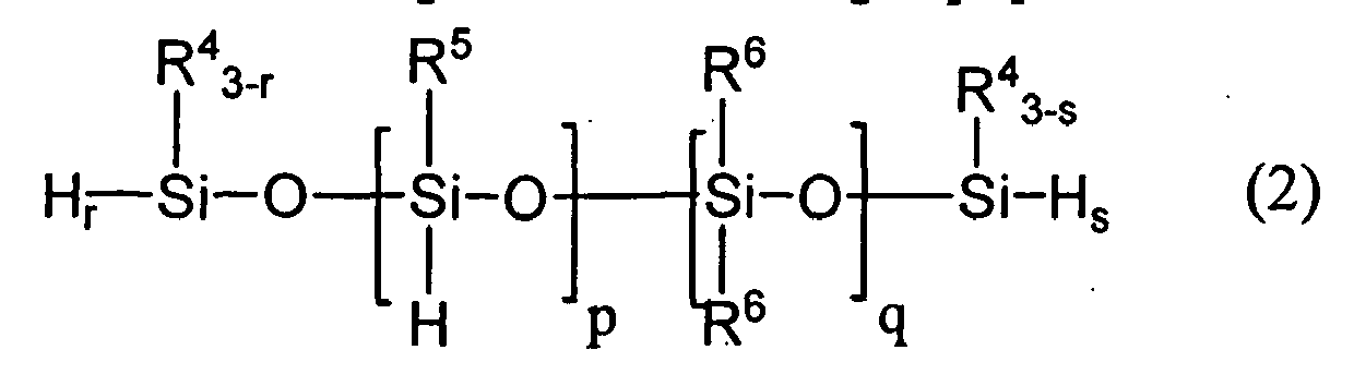 (B2) a branched organohydrogenpolysiloxane that is liquid at 25°C,(C) a platinum group metal catalyst in an effective amount, and(D) a linear or cyclic organopolysiloxane of 4 to 50 silicon atoms, having at least two functional groups selected from the group consisting of silicon atom-bonded alkenyl groups, alkoxysilyl groups and epoxy groups: in an amount within a range from 0.01 to 10 parts by mass per 100 parts by mass of the component (A).
 - The composition according to claim 1, wherein the component (A) contains 0.007 to 0.04 mols of alkenyl groups per 100 g thereof.
- The composition according to claim 1, wherein the linear organopolysiloxane of the component (A1) has alkenyl groups of 2 to 8 carbon atoms at both terminal ends.
- The composition according to claim 1, wherein the linear organopolysiloxane of the component (A1) has a viscosity at 25°C of 100 to 100,000 mPa·s.
- The composition according to claim 1, wherein the component (A2) contains SiO2 units in an amount of 1 mol% to 70 mol% of the entire siloxane units contained in the component.
- The composition according to claim 1, wherein the component (A2) contains at least two alkenyl groups per molecule.
- The composition according to claim 1, wherein the mass ratio of the component (A1)/component (A2) is in a range from 70/30 to 90/10.
- The composition according to claim 1, wherein the molar ratio of alkenyl groups within the component (A1) to alkenyl groups within the component (A2) is within a range from 1/2 to 1/30.
- The composition according to claim 1, wherein a molar ratio of [SiH groups within the component (B) / alkenyl groups within the component (A)] is within a range from 1 to 2.
- The composition according to claim 1, wherein the organohydrogenpolysiloxane of the component (B1) contains at least two SiH groups per molecule.
- The composition according to claim 1, wherein the organohydrogenpolysiloxane of the component (B1) is represented by the formula (2):

- The composition according to claim 1, wherein the molar ratio of [SiH groups within component (B1) / SiH groups within component (B2)] is within a range from 60/40 to 80/20.
- An optical semiconductor device, comprising an optical semiconductor element, and a layer formed of a cured product of a composition defined in claim 1 that covers the optical semiconductor element.
- The optical semiconductor device according to claim 13, wherein the optical semiconductor element is a light emitting diode.
Applications Claiming Priority (1)
| Application Number | Priority Date | Filing Date | Title |
|---|---|---|---|
| JP2009050737 | 2009-03-04 |
Publications (2)
| Publication Number | Publication Date |
|---|---|
| EP2226360A1 true EP2226360A1 (en) | 2010-09-08 |
| EP2226360B1 EP2226360B1 (en) | 2014-05-07 |
Family
ID=42313698
Family Applications (1)
| Application Number | Title | Priority Date | Filing Date |
|---|---|---|---|
| EP10002174.0A Active EP2226360B1 (en) | 2009-03-04 | 2010-03-03 | Composition for encapsulating optical semiconductor and optical semiconductor device using same |
Country Status (6)
| Country | Link |
|---|---|
| US (1) | US8373196B2 (en) |
| EP (1) | EP2226360B1 (en) |
| JP (1) | JP5499774B2 (en) |
| KR (1) | KR101660982B1 (en) |
| CN (1) | CN101824222B (en) |
| TW (1) | TWI448514B (en) |
Cited By (6)
| Publication number | Priority date | Publication date | Assignee | Title |
|---|---|---|---|---|
| EP2530752A3 (en) * | 2011-06-01 | 2013-11-13 | Nitto Denko Corporation | Reflecting material and light emitting diode device |
| EP2657300A4 (en) * | 2010-12-22 | 2014-08-20 | Momentive Performance Mat Jp | THERMOSETTING POLYORGANOSILOXANE COMPOSITION AND USE THEREOF |
| EP2784127A4 (en) * | 2011-11-25 | 2015-07-29 | Lg Chemical Ltd | CURABLE COMPOSITION |
| EP2878635A4 (en) * | 2012-07-27 | 2016-01-06 | Lg Chemical Ltd | CURING COMPOSITION |
| EP3101062A1 (en) * | 2015-06-05 | 2016-12-07 | Shin-Etsu Chemical Co., Ltd. | Nanoparticle, method for producing nanoparticle, addition curing silicone resin composition, and semiconductor apparatus |
| US10125242B2 (en) | 2014-05-30 | 2018-11-13 | Dow Corning Toray Co., Ltd. | Organosilicon compound, curable silicone composition, and semiconductor device |
Families Citing this family (43)
| Publication number | Priority date | Publication date | Assignee | Title |
|---|---|---|---|---|
| JP5549568B2 (en) * | 2009-12-15 | 2014-07-16 | 信越化学工業株式会社 | Resin composition for sealing optical semiconductor element and optical semiconductor device sealed with the composition |
| JP5844252B2 (en) * | 2010-04-02 | 2016-01-13 | 株式会社カネカ | Curable resin composition, curable resin composition tablet, molded product, semiconductor package, semiconductor component, and light emitting diode |
| JP5002075B2 (en) * | 2010-10-14 | 2012-08-15 | モメンティブ・パフォーマンス・マテリアルズ・ジャパン合同会社 | Curable polyorganosiloxane composition |
| JP5490671B2 (en) * | 2010-12-07 | 2014-05-14 | 信越化学工業株式会社 | Method for curing silicone resin composition |
| TWI435914B (en) | 2010-12-31 | 2014-05-01 | Eternal Chemical Co Ltd | Curable organic polyoxane composition and preparation method thereof |
| CN103619958B (en) * | 2011-03-28 | 2016-06-29 | 汉高股份有限及两合公司 | Curable Silicone Resins for LED Encapsulation |
| CN102751420A (en) * | 2011-04-19 | 2012-10-24 | 菱生精密工业股份有限公司 | Light-emitting diode packaging structure |
| JP5522116B2 (en) * | 2011-04-28 | 2014-06-18 | 信越化学工業株式会社 | Addition-curing silicone composition and optical semiconductor device using the same |
| CN102408723A (en) * | 2011-08-08 | 2012-04-11 | 吴世维 | Silicone rubber, silicone rubber manufacturing method and feeding bottle manufactured by silicone rubber |
| JP6057503B2 (en) * | 2011-09-21 | 2017-01-11 | 東レ・ダウコーニング株式会社 | Curable silicone composition for encapsulating optical semiconductor element, method for producing resin-encapsulated optical semiconductor element, and resin-encapsulated optical semiconductor element |
| JP5653877B2 (en) * | 2011-10-04 | 2015-01-14 | 信越化学工業株式会社 | Curable composition for sealing optical semiconductor and optical semiconductor device using the same |
| KR101443979B1 (en) | 2011-11-25 | 2014-09-23 | 주식회사 엘지화학 | Curable composition |
| TWI498356B (en) | 2011-11-25 | 2015-09-01 | Lg化學股份有限公司 | Organic polyoxane |
| WO2013077700A1 (en) * | 2011-11-25 | 2013-05-30 | 주식회사 엘지화학 | Curable composition |
| EP2784129B1 (en) * | 2011-11-25 | 2017-04-26 | LG Chem, Ltd. | Curable composition |
| TWI480335B (en) * | 2011-11-25 | 2015-04-11 | Lg化學股份有限公司 | Curable composition |
| TWI480316B (en) * | 2012-07-13 | 2015-04-11 | Daxin Materials Corp | Star-shaped polysiloxane containing alkenyl group or silicon-hydrogen bond and thermal curable resin composition |
| JP5985981B2 (en) * | 2012-12-28 | 2016-09-06 | 東レ・ダウコーニング株式会社 | Curable silicone composition, cured product thereof, and optical semiconductor device |
| CN103408945B (en) * | 2013-02-18 | 2016-01-20 | 永信新材料有限公司 | Polysiloxane composition applicable to light-emitting diode components, base formulation and light-emitting diode components thereof |
| KR101667839B1 (en) * | 2013-04-04 | 2016-10-19 | 주식회사 엘지화학 | Curable composition |
| TWI490276B (en) * | 2013-07-30 | 2015-07-01 | Chi Mei Corp | Silicone resin encapsulant and light emitting diode device |
| KR102185308B1 (en) * | 2013-10-30 | 2020-12-01 | 신에쓰 가가꾸 고교 가부시끼가이샤 | Curable composition for sealing optical semiconductor and optical semiconductor device using the same |
| JP6276166B2 (en) * | 2014-10-01 | 2018-02-07 | 信越化学工業株式会社 | Curable composition for sealing optical semiconductor and optical semiconductor device using the same |
| CN105482429B (en) * | 2014-10-01 | 2019-04-30 | 信越化学工业株式会社 | Curable composition for optical semiconductor sealing and optical semiconductor device using the same |
| CN105713391B (en) * | 2014-12-03 | 2018-11-09 | 广州慧谷化学有限公司 | Thixotropic organopolysiloxane composition and semiconductor devices |
| CN105985649B (en) * | 2015-01-30 | 2019-03-19 | 广州慧谷化学有限公司 | Curable block organopolysiloxane composition and semiconductor device |
| JP6633859B2 (en) * | 2015-07-31 | 2020-01-22 | ルネサスエレクトロニクス株式会社 | Semiconductor device |
| WO2017147061A1 (en) * | 2016-02-23 | 2017-08-31 | Dow Corning Corporation | Selective adhesion silicone rubber |
| CN106010424A (en) * | 2016-06-28 | 2016-10-12 | 华蓥市高科龙电子科技有限公司 | LED (light emitting diode) encapsulation material |
| CN111918928B (en) * | 2018-03-20 | 2022-12-20 | 信越化学工业株式会社 | Silicone gel composition, cured product thereof, and power module |
| JP6969675B2 (en) * | 2018-04-16 | 2021-11-24 | 信越化学工業株式会社 | Transparent desiccant for organic EL and how to use it |
| KR20210080434A (en) * | 2018-10-18 | 2021-06-30 | 다우 도레이 캄파니 리미티드 | Curable silicone composition and cured product thereof, laminate and manufacturing method thereof, and optical device or optical display |
| US11981776B2 (en) | 2018-10-18 | 2024-05-14 | Dow Toray Co., Ltd. | Curable silicone composition and cured product thereof, layered product and production method therefor, and optical device or optical display |
| WO2020080350A1 (en) | 2018-10-18 | 2020-04-23 | ダウ・東レ株式会社 | Curable silicone composition and cured product of same, multilayer body and method for producing same, and optical device or optical display |
| JP6966411B2 (en) * | 2018-11-02 | 2021-11-17 | 信越化学工業株式会社 | Additive-curable silicone resin composition, cured product thereof, and optical semiconductor device |
| CN111909517B (en) * | 2019-05-10 | 2022-03-01 | 中国科学院化学研究所 | Organosilicon composition capable of being subjected to ring-line crosslinking, reaction product, preparation method and application |
| JP7475135B2 (en) * | 2019-12-25 | 2024-04-26 | デュポン・東レ・スペシャルティ・マテリアル株式会社 | Curable white silicone composition, reflector for optical semiconductor device, and optical semiconductor device |
| KR102467690B1 (en) * | 2020-08-19 | 2022-11-17 | 주식회사 케이씨씨실리콘 | Polysiloxane composition for optical use and reflective materials for optical semiconductor comprising the same |
| JP7578279B2 (en) * | 2020-12-28 | 2024-11-06 | デュポン・東レ・スペシャルティ・マテリアル株式会社 | CURABLE SILICONE COMPOSITION, ENCAPSULATING MATERIAL, AND OPTICAL SEMICONDUCTOR DEVICE |
| JP2022118487A (en) * | 2021-02-02 | 2022-08-15 | ウシオ電機株式会社 | Optical semiconductor device and method for manufacturing the same |
| JP7759272B2 (en) * | 2022-01-31 | 2025-10-23 | 信越化学工業株式会社 | Curable organopolysiloxane composition and semiconductor device for wearable device |
| JP2023132308A (en) * | 2022-03-10 | 2023-09-22 | デュポン・東レ・スペシャルティ・マテリアル株式会社 | curable silicone composition |
| JP2023132309A (en) | 2022-03-10 | 2023-09-22 | デュポン・東レ・スペシャルティ・マテリアル株式会社 | curable silicone composition |
Citations (3)
| Publication number | Priority date | Publication date | Assignee | Title |
|---|---|---|---|---|
| US20070077360A1 (en) | 2005-09-30 | 2007-04-05 | Shin -Etsu Chemical Co., Ltd. | Method of reducing surface tackiness of silicone rubber cured product, liquid silicone rubber composition for sealing semiconductor, silicone rubber-sealed semiconductor device, and method of producing semiconductor device |
| JP2007103494A (en) | 2005-09-30 | 2007-04-19 | Nichia Chem Ind Ltd | Silicone rubber-sealed light emitting device and method for manufacturing the light emitting device |
| US20070106016A1 (en) * | 2005-11-09 | 2007-05-10 | Aijun Zhu | Silicone elastomer composition |
Family Cites Families (18)
| Publication number | Priority date | Publication date | Assignee | Title |
|---|---|---|---|---|
| US3996195A (en) * | 1974-11-15 | 1976-12-07 | Shinetsu Chemical Company | Curable organosilicon compositions |
| JPS5239751A (en) * | 1975-09-26 | 1977-03-28 | Shin Etsu Chem Co Ltd | Curable organopolysiloxane compositions |
| US4427801A (en) * | 1982-04-14 | 1984-01-24 | Dow Corning Corporation | Extrudable silicone elastomer compositions |
| JPS6183251A (en) * | 1984-10-01 | 1986-04-26 | Shin Etsu Chem Co Ltd | Curable organopolysiloxane composition |
| US5082886A (en) * | 1989-08-28 | 1992-01-21 | General Electric Company | Low compression set, oil and fuel resistant, liquid injection moldable, silicone rubber |
| US5198479A (en) * | 1990-08-24 | 1993-03-30 | Shin-Etsu Chemical Company Limited | Light transmissive epoxy resin compositions and optical semiconductor devices encapsulated therewith |
| US6124407A (en) * | 1998-10-28 | 2000-09-26 | Dow Corning Corporation | Silicone composition, method for the preparation thereof, and silicone elastomer |
| JP3523098B2 (en) * | 1998-12-28 | 2004-04-26 | 信越化学工業株式会社 | Addition-curable silicone composition |
| JP3865639B2 (en) * | 2002-01-28 | 2007-01-10 | 信越化学工業株式会社 | Silicone composition for semiconductor encapsulation and semiconductor device |
| JP4409160B2 (en) * | 2002-10-28 | 2010-02-03 | 東レ・ダウコーニング株式会社 | Curable organopolysiloxane composition and semiconductor device |
| JP4154605B2 (en) * | 2004-01-23 | 2008-09-24 | 信越化学工業株式会社 | Thermally conductive silicone heat dissipation composition and method for manufacturing heat dissipation structure |
| JP4300418B2 (en) * | 2004-04-30 | 2009-07-22 | 信越化学工業株式会社 | Epoxy / silicone hybrid resin composition and light emitting semiconductor device |
| JP4455218B2 (en) * | 2004-08-12 | 2010-04-21 | 信越化学工業株式会社 | Self-adhesive addition reaction curable silicone composition |
| JP4623282B2 (en) * | 2005-03-10 | 2011-02-02 | 信越化学工業株式会社 | Manufacturing method of semiconductor device |
| US7588967B2 (en) * | 2005-05-27 | 2009-09-15 | Shin-Etsu Chemical Co., Ltd. | Curable silicone rubber composition and semiconductor device |
| JP2007063538A (en) * | 2005-08-03 | 2007-03-15 | Shin Etsu Chem Co Ltd | Addition-curing silicone resin composition for light-emitting diodes |
| TWI434890B (en) * | 2007-04-06 | 2014-04-21 | Shinetsu Chemical Co | Addition curable silicone resin composition and silicone lens using same |
| JP5526823B2 (en) * | 2009-02-24 | 2014-06-18 | 信越化学工業株式会社 | Optical semiconductor device sealed with silicone resin |
-
2010
- 2010-03-02 JP JP2010044910A patent/JP5499774B2/en active Active
- 2010-03-03 KR KR1020100018794A patent/KR101660982B1/en active Active
- 2010-03-03 TW TW099106113A patent/TWI448514B/en active
- 2010-03-03 EP EP10002174.0A patent/EP2226360B1/en active Active
- 2010-03-03 US US12/716,823 patent/US8373196B2/en active Active
- 2010-03-04 CN CN2010101298630A patent/CN101824222B/en active Active
Patent Citations (3)
| Publication number | Priority date | Publication date | Assignee | Title |
|---|---|---|---|---|
| US20070077360A1 (en) | 2005-09-30 | 2007-04-05 | Shin -Etsu Chemical Co., Ltd. | Method of reducing surface tackiness of silicone rubber cured product, liquid silicone rubber composition for sealing semiconductor, silicone rubber-sealed semiconductor device, and method of producing semiconductor device |
| JP2007103494A (en) | 2005-09-30 | 2007-04-19 | Nichia Chem Ind Ltd | Silicone rubber-sealed light emitting device and method for manufacturing the light emitting device |
| US20070106016A1 (en) * | 2005-11-09 | 2007-05-10 | Aijun Zhu | Silicone elastomer composition |
Cited By (11)
| Publication number | Priority date | Publication date | Assignee | Title |
|---|---|---|---|---|
| EP2657300A4 (en) * | 2010-12-22 | 2014-08-20 | Momentive Performance Mat Jp | THERMOSETTING POLYORGANOSILOXANE COMPOSITION AND USE THEREOF |
| US9540551B2 (en) | 2010-12-22 | 2017-01-10 | Momentive Performance Materials Japan Llc | Heat-curable polyorganosiloxane composition and use thereof |
| EP2530752A3 (en) * | 2011-06-01 | 2013-11-13 | Nitto Denko Corporation | Reflecting material and light emitting diode device |
| US8723167B2 (en) | 2011-06-01 | 2014-05-13 | Nitto Denko Corporation | Reflecting material and light emitting diode device |
| EP2784127A4 (en) * | 2011-11-25 | 2015-07-29 | Lg Chemical Ltd | CURABLE COMPOSITION |
| US9177883B2 (en) | 2011-11-25 | 2015-11-03 | Lg Chem, Ltd. | Curable composition |
| EP2878635A4 (en) * | 2012-07-27 | 2016-01-06 | Lg Chemical Ltd | CURING COMPOSITION |
| US9355926B2 (en) | 2012-07-27 | 2016-05-31 | Lg Chem, Ltd. | Curable composition |
| US10125242B2 (en) | 2014-05-30 | 2018-11-13 | Dow Corning Toray Co., Ltd. | Organosilicon compound, curable silicone composition, and semiconductor device |
| EP3101062A1 (en) * | 2015-06-05 | 2016-12-07 | Shin-Etsu Chemical Co., Ltd. | Nanoparticle, method for producing nanoparticle, addition curing silicone resin composition, and semiconductor apparatus |
| US9695301B2 (en) | 2015-06-05 | 2017-07-04 | Shin-Etsu Chemical Co., Ltd. | Nanoparticle, method for producing nanoparticle, addition curing silicone resin composition, and semiconductor apparatus |
Also Published As
| Publication number | Publication date |
|---|---|
| EP2226360B1 (en) | 2014-05-07 |
| KR101660982B1 (en) | 2016-09-28 |
| US8373196B2 (en) | 2013-02-12 |
| CN101824222A (en) | 2010-09-08 |
| JP2010229402A (en) | 2010-10-14 |
| TWI448514B (en) | 2014-08-11 |
| JP5499774B2 (en) | 2014-05-21 |
| US20100224906A1 (en) | 2010-09-09 |
| CN101824222B (en) | 2012-08-29 |
| KR20100100634A (en) | 2010-09-15 |
| TW201040229A (en) | 2010-11-16 |
Similar Documents
| Publication | Publication Date | Title |
|---|---|---|
| EP2226360B1 (en) | Composition for encapsulating optical semiconductor and optical semiconductor device using same | |
| EP2221868B1 (en) | Optical semiconductor device encapsulated with silicone resin | |
| EP2105466B1 (en) | Curable silicone rubber composition and semiconductor devices | |
| CN105121556B (en) | Curable silicone composition, cured product thereof, and optical semiconductor device | |
| US9012586B2 (en) | Curable organopolysiloxane composition and optical semiconductor device | |
| EP2588538B1 (en) | Curable organopolysiloxane composition and optical semiconductor device | |
| KR101911690B1 (en) | Curable silicone composition and optical semiconductor device | |
| KR102933338B1 (en) | Curable silicone composition, encapsulant and optical semiconductor device | |
| JP2017088644A (en) | Adhesion promotor, addition reaction curable organopolysiloxane resin composition, and semiconductor device | |
| KR20150050401A (en) | Curable composition for sealing optical semiconductor and optical semiconductor device using the same | |
| KR20230133239A (en) | Curable silicone composition | |
| TWI681996B (en) | Hardening composition for optical semiconductor sealing and optical semiconductor device using the composition |
Legal Events
| Date | Code | Title | Description |
|---|---|---|---|
| PUAI | Public reference made under article 153(3) epc to a published international application that has entered the european phase |
Free format text: ORIGINAL CODE: 0009012 |
|
| AK | Designated contracting states |
Kind code of ref document: A1 Designated state(s): AT BE BG CH CY CZ DE DK EE ES FI FR GB GR HR HU IE IS IT LI LT LU LV MC MK MT NL NO PL PT RO SE SI SK SM TR |
|
| AX | Request for extension of the european patent |
Extension state: AL BA ME RS |
|
| 17P | Request for examination filed |
Effective date: 20110302 |
|
| GRAP | Despatch of communication of intention to grant a patent |
Free format text: ORIGINAL CODE: EPIDOSNIGR1 |
|
| RAP1 | Party data changed (applicant data changed or rights of an application transferred) |
Owner name: SHIN-ETSU CHEMICAL CO., LTD. |
|
| INTG | Intention to grant announced |
Effective date: 20140102 |
|
| GRAS | Grant fee paid |
Free format text: ORIGINAL CODE: EPIDOSNIGR3 |
|
| GRAA | (expected) grant |
Free format text: ORIGINAL CODE: 0009210 |
|
| AK | Designated contracting states |
Kind code of ref document: B1 Designated state(s): AT BE BG CH CY CZ DE DK EE ES FI FR GB GR HR HU IE IS IT LI LT LU LV MC MK MT NL NO PL PT RO SE SI SK SM TR |
|
| REG | Reference to a national code |
Ref country code: GB Ref legal event code: FG4D |
|
| REG | Reference to a national code |
Ref country code: AT Ref legal event code: REF Ref document number: 666681 Country of ref document: AT Kind code of ref document: T Effective date: 20140515 |
|
| REG | Reference to a national code |
Ref country code: IE Ref legal event code: FG4D |
|
| REG | Reference to a national code |
Ref country code: DE Ref legal event code: R096 Ref document number: 602010015737 Country of ref document: DE Effective date: 20140618 |
|
| REG | Reference to a national code |
Ref country code: AT Ref legal event code: MK05 Ref document number: 666681 Country of ref document: AT Kind code of ref document: T Effective date: 20140507 |
|
| REG | Reference to a national code |
Ref country code: NL Ref legal event code: VDEP Effective date: 20140507 |
|
| REG | Reference to a national code |
Ref country code: LT Ref legal event code: MG4D |
|
| PG25 | Lapsed in a contracting state [announced via postgrant information from national office to epo] |
Ref country code: FI Free format text: LAPSE BECAUSE OF FAILURE TO SUBMIT A TRANSLATION OF THE DESCRIPTION OR TO PAY THE FEE WITHIN THE PRESCRIBED TIME-LIMIT Effective date: 20140507 Ref country code: IS Free format text: LAPSE BECAUSE OF FAILURE TO SUBMIT A TRANSLATION OF THE DESCRIPTION OR TO PAY THE FEE WITHIN THE PRESCRIBED TIME-LIMIT Effective date: 20140907 Ref country code: LT Free format text: LAPSE BECAUSE OF FAILURE TO SUBMIT A TRANSLATION OF THE DESCRIPTION OR TO PAY THE FEE WITHIN THE PRESCRIBED TIME-LIMIT Effective date: 20140507 Ref country code: NO Free format text: LAPSE BECAUSE OF FAILURE TO SUBMIT A TRANSLATION OF THE DESCRIPTION OR TO PAY THE FEE WITHIN THE PRESCRIBED TIME-LIMIT Effective date: 20140807 Ref country code: CY Free format text: LAPSE BECAUSE OF FAILURE TO SUBMIT A TRANSLATION OF THE DESCRIPTION OR TO PAY THE FEE WITHIN THE PRESCRIBED TIME-LIMIT Effective date: 20140507 Ref country code: GR Free format text: LAPSE BECAUSE OF FAILURE TO SUBMIT A TRANSLATION OF THE DESCRIPTION OR TO PAY THE FEE WITHIN THE PRESCRIBED TIME-LIMIT Effective date: 20140808 |
|
| PG25 | Lapsed in a contracting state [announced via postgrant information from national office to epo] |
Ref country code: PL Free format text: LAPSE BECAUSE OF FAILURE TO SUBMIT A TRANSLATION OF THE DESCRIPTION OR TO PAY THE FEE WITHIN THE PRESCRIBED TIME-LIMIT Effective date: 20140507 Ref country code: ES Free format text: LAPSE BECAUSE OF FAILURE TO SUBMIT A TRANSLATION OF THE DESCRIPTION OR TO PAY THE FEE WITHIN THE PRESCRIBED TIME-LIMIT Effective date: 20140507 Ref country code: SE Free format text: LAPSE BECAUSE OF FAILURE TO SUBMIT A TRANSLATION OF THE DESCRIPTION OR TO PAY THE FEE WITHIN THE PRESCRIBED TIME-LIMIT Effective date: 20140507 Ref country code: AT Free format text: LAPSE BECAUSE OF FAILURE TO SUBMIT A TRANSLATION OF THE DESCRIPTION OR TO PAY THE FEE WITHIN THE PRESCRIBED TIME-LIMIT Effective date: 20140507 Ref country code: LV Free format text: LAPSE BECAUSE OF FAILURE TO SUBMIT A TRANSLATION OF THE DESCRIPTION OR TO PAY THE FEE WITHIN THE PRESCRIBED TIME-LIMIT Effective date: 20140507 Ref country code: HR Free format text: LAPSE BECAUSE OF FAILURE TO SUBMIT A TRANSLATION OF THE DESCRIPTION OR TO PAY THE FEE WITHIN THE PRESCRIBED TIME-LIMIT Effective date: 20140507 |
|
| PG25 | Lapsed in a contracting state [announced via postgrant information from national office to epo] |
Ref country code: PT Free format text: LAPSE BECAUSE OF FAILURE TO SUBMIT A TRANSLATION OF THE DESCRIPTION OR TO PAY THE FEE WITHIN THE PRESCRIBED TIME-LIMIT Effective date: 20140908 |
|
| PG25 | Lapsed in a contracting state [announced via postgrant information from national office to epo] |
Ref country code: RO Free format text: LAPSE BECAUSE OF FAILURE TO SUBMIT A TRANSLATION OF THE DESCRIPTION OR TO PAY THE FEE WITHIN THE PRESCRIBED TIME-LIMIT Effective date: 20140507 Ref country code: CZ Free format text: LAPSE BECAUSE OF FAILURE TO SUBMIT A TRANSLATION OF THE DESCRIPTION OR TO PAY THE FEE WITHIN THE PRESCRIBED TIME-LIMIT Effective date: 20140507 Ref country code: SK Free format text: LAPSE BECAUSE OF FAILURE TO SUBMIT A TRANSLATION OF THE DESCRIPTION OR TO PAY THE FEE WITHIN THE PRESCRIBED TIME-LIMIT Effective date: 20140507 Ref country code: EE Free format text: LAPSE BECAUSE OF FAILURE TO SUBMIT A TRANSLATION OF THE DESCRIPTION OR TO PAY THE FEE WITHIN THE PRESCRIBED TIME-LIMIT Effective date: 20140507 Ref country code: BE Free format text: LAPSE BECAUSE OF FAILURE TO SUBMIT A TRANSLATION OF THE DESCRIPTION OR TO PAY THE FEE WITHIN THE PRESCRIBED TIME-LIMIT Effective date: 20140507 Ref country code: DK Free format text: LAPSE BECAUSE OF FAILURE TO SUBMIT A TRANSLATION OF THE DESCRIPTION OR TO PAY THE FEE WITHIN THE PRESCRIBED TIME-LIMIT Effective date: 20140507 |
|
| REG | Reference to a national code |
Ref country code: DE Ref legal event code: R097 Ref document number: 602010015737 Country of ref document: DE |
|
| PG25 | Lapsed in a contracting state [announced via postgrant information from national office to epo] |
Ref country code: NL Free format text: LAPSE BECAUSE OF FAILURE TO SUBMIT A TRANSLATION OF THE DESCRIPTION OR TO PAY THE FEE WITHIN THE PRESCRIBED TIME-LIMIT Effective date: 20140507 |
|
| PLBE | No opposition filed within time limit |
Free format text: ORIGINAL CODE: 0009261 |
|
| STAA | Information on the status of an ep patent application or granted ep patent |
Free format text: STATUS: NO OPPOSITION FILED WITHIN TIME LIMIT |
|
| 26N | No opposition filed |
Effective date: 20150210 |
|
| PG25 | Lapsed in a contracting state [announced via postgrant information from national office to epo] |
Ref country code: IT Free format text: LAPSE BECAUSE OF FAILURE TO SUBMIT A TRANSLATION OF THE DESCRIPTION OR TO PAY THE FEE WITHIN THE PRESCRIBED TIME-LIMIT Effective date: 20140507 |
|
| REG | Reference to a national code |
Ref country code: DE Ref legal event code: R097 Ref document number: 602010015737 Country of ref document: DE Effective date: 20150210 |
|
| PG25 | Lapsed in a contracting state [announced via postgrant information from national office to epo] |
Ref country code: SI Free format text: LAPSE BECAUSE OF FAILURE TO SUBMIT A TRANSLATION OF THE DESCRIPTION OR TO PAY THE FEE WITHIN THE PRESCRIBED TIME-LIMIT Effective date: 20140507 |
|
| PG25 | Lapsed in a contracting state [announced via postgrant information from national office to epo] |
Ref country code: LU Free format text: LAPSE BECAUSE OF FAILURE TO SUBMIT A TRANSLATION OF THE DESCRIPTION OR TO PAY THE FEE WITHIN THE PRESCRIBED TIME-LIMIT Effective date: 20150303 Ref country code: MC Free format text: LAPSE BECAUSE OF FAILURE TO SUBMIT A TRANSLATION OF THE DESCRIPTION OR TO PAY THE FEE WITHIN THE PRESCRIBED TIME-LIMIT Effective date: 20140507 |
|
| REG | Reference to a national code |
Ref country code: CH Ref legal event code: PL |
|
| GBPC | Gb: european patent ceased through non-payment of renewal fee |
Effective date: 20150303 |
|
| REG | Reference to a national code |
Ref country code: FR Ref legal event code: ST Effective date: 20151130 |
|
| REG | Reference to a national code |
Ref country code: IE Ref legal event code: MM4A |
|
| PG25 | Lapsed in a contracting state [announced via postgrant information from national office to epo] |
Ref country code: LI Free format text: LAPSE BECAUSE OF NON-PAYMENT OF DUE FEES Effective date: 20150331 Ref country code: CH Free format text: LAPSE BECAUSE OF NON-PAYMENT OF DUE FEES Effective date: 20150331 Ref country code: GB Free format text: LAPSE BECAUSE OF NON-PAYMENT OF DUE FEES Effective date: 20150303 Ref country code: IE Free format text: LAPSE BECAUSE OF NON-PAYMENT OF DUE FEES Effective date: 20150303 |
|
| PG25 | Lapsed in a contracting state [announced via postgrant information from national office to epo] |
Ref country code: FR Free format text: LAPSE BECAUSE OF NON-PAYMENT OF DUE FEES Effective date: 20150331 |
|
| PG25 | Lapsed in a contracting state [announced via postgrant information from national office to epo] |
Ref country code: MT Free format text: LAPSE BECAUSE OF FAILURE TO SUBMIT A TRANSLATION OF THE DESCRIPTION OR TO PAY THE FEE WITHIN THE PRESCRIBED TIME-LIMIT Effective date: 20140507 |
|
| PG25 | Lapsed in a contracting state [announced via postgrant information from national office to epo] |
Ref country code: HU Free format text: LAPSE BECAUSE OF FAILURE TO SUBMIT A TRANSLATION OF THE DESCRIPTION OR TO PAY THE FEE WITHIN THE PRESCRIBED TIME-LIMIT; INVALID AB INITIO Effective date: 20100303 Ref country code: BG Free format text: LAPSE BECAUSE OF FAILURE TO SUBMIT A TRANSLATION OF THE DESCRIPTION OR TO PAY THE FEE WITHIN THE PRESCRIBED TIME-LIMIT Effective date: 20140507 Ref country code: SM Free format text: LAPSE BECAUSE OF FAILURE TO SUBMIT A TRANSLATION OF THE DESCRIPTION OR TO PAY THE FEE WITHIN THE PRESCRIBED TIME-LIMIT Effective date: 20140507 |
|
| PG25 | Lapsed in a contracting state [announced via postgrant information from national office to epo] |
Ref country code: TR Free format text: LAPSE BECAUSE OF FAILURE TO SUBMIT A TRANSLATION OF THE DESCRIPTION OR TO PAY THE FEE WITHIN THE PRESCRIBED TIME-LIMIT Effective date: 20140507 |
|
| PG25 | Lapsed in a contracting state [announced via postgrant information from national office to epo] |
Ref country code: MK Free format text: LAPSE BECAUSE OF FAILURE TO SUBMIT A TRANSLATION OF THE DESCRIPTION OR TO PAY THE FEE WITHIN THE PRESCRIBED TIME-LIMIT Effective date: 20140507 |
|
| REG | Reference to a national code |
Ref country code: DE Ref legal event code: R082 Ref document number: 602010015737 Country of ref document: DE Representative=s name: ZACCO LEGAL RECHTSANWALTSGESELLSCHAFT MBH, DE |
|
| REG | Reference to a national code |
Ref country code: DE Ref legal event code: R082 Ref document number: 602010015737 Country of ref document: DE |
|
| PGFP | Annual fee paid to national office [announced via postgrant information from national office to epo] |
Ref country code: DE Payment date: 20260128 Year of fee payment: 17 |