EP2224793A1 - Circuit board and circuit board assembly - Google Patents
Circuit board and circuit board assembly Download PDFInfo
- Publication number
- EP2224793A1 EP2224793A1 EP10151320A EP10151320A EP2224793A1 EP 2224793 A1 EP2224793 A1 EP 2224793A1 EP 10151320 A EP10151320 A EP 10151320A EP 10151320 A EP10151320 A EP 10151320A EP 2224793 A1 EP2224793 A1 EP 2224793A1
- Authority
- EP
- European Patent Office
- Prior art keywords
- patterns
- circuit board
- static electricity
- angular parts
- circuit
- Prior art date
- Legal status (The legal status is an assumption and is not a legal conclusion. Google has not performed a legal analysis and makes no representation as to the accuracy of the status listed.)
- Withdrawn
Links
- 230000005611 electricity Effects 0.000 claims abstract description 51
- 230000003068 static effect Effects 0.000 claims abstract description 51
- 230000001681 protective effect Effects 0.000 description 2
- 230000000712 assembly Effects 0.000 description 1
- 238000000429 assembly Methods 0.000 description 1
- 238000010586 diagram Methods 0.000 description 1
- 238000010137 moulding (plastic) Methods 0.000 description 1
- 229910052755 nonmetal Inorganic materials 0.000 description 1
Images

Classifications
-
- H—ELECTRICITY
- H05—ELECTRIC TECHNIQUES NOT OTHERWISE PROVIDED FOR
- H05K—PRINTED CIRCUITS; CASINGS OR CONSTRUCTIONAL DETAILS OF ELECTRIC APPARATUS; MANUFACTURE OF ASSEMBLAGES OF ELECTRICAL COMPONENTS
- H05K1/00—Printed circuits
- H05K1/02—Details
- H05K1/0213—Electrical arrangements not otherwise provided for
- H05K1/0254—High voltage adaptations; Electrical insulation details; Overvoltage or electrostatic discharge protection ; Arrangements for regulating voltages or for using plural voltages
- H05K1/0257—Overvoltage protection
- H05K1/026—Spark gaps
-
- H—ELECTRICITY
- H05—ELECTRIC TECHNIQUES NOT OTHERWISE PROVIDED FOR
- H05K—PRINTED CIRCUITS; CASINGS OR CONSTRUCTIONAL DETAILS OF ELECTRIC APPARATUS; MANUFACTURE OF ASSEMBLAGES OF ELECTRICAL COMPONENTS
- H05K2201/00—Indexing scheme relating to printed circuits covered by H05K1/00
- H05K2201/09—Shape and layout
- H05K2201/09209—Shape and layout details of conductors
- H05K2201/09654—Shape and layout details of conductors covering at least two types of conductors provided for in H05K2201/09218 - H05K2201/095
- H05K2201/09727—Varying width along a single conductor; Conductors or pads having different widths
Definitions
- the present invention relates to a circuit board mounted on an electronic device or a component constituting an electronic device, and in particular, relates to a static-proof circuit board and circuit board assembly.
- circuit boards mounted on electronic devices are made proof against static electricity in order to protect circuit components.
- a discharge of static electricity occurs in the vicinity of a circuit board provided with a plurality of circuit patterns, it is difficult to specify through which circuit pattern discharge current flows to the ground.
- an antistatic component i.e., a component that dissipates static electricity
- Fig. 3 is a plan view of a circuit board 100 built in a wiper switch in a car.
- the circuit board 100 is provided with four kinds of circuit patterns 101 to 104.
- An antistatic component (not shown) is provided for each of these circuit patterns 101 to 104.
- Discharges due to static electricity include a discharge of charge accumulated in or on a human body. For example, assuming that a person gets on a car in a dry season, charge is generated by the friction between clothes of the person and a sheet, so that the charge is accumulated on the clothes. For example, when a driver operates a slide switch for wiper time control disposed in a wiper lever, the charge (static electricity) accumulated on the clothes of the driver may be discharged through a slight gap in the slide switch to a circuit pattern in a circuit board (refer to Fig. 3 ) received in the wiper lever.
- Fig. 4 is a perspective view illustrating a wiper lever in a car.
- a slide switch 111 for wiper time control is disposed in an end portion of a wiper lever 110.
- Charge accumulated on clothes of a driver flows through any gap between a main body of the lever 110 and the slide switch 111, i.e., a gap adjacent to the proximal end of the wiper lever 110 or a gap 112 adjacent to the distal end thereof, thus causing a discharge of the charge in a circuit board built in the wiper lever 110.
- an area 105 surrounded by a dashed line in the circuit board 100 shown in Fig. 3 corresponds to the position of the slide switch 111 in the wiper lever 110.
- This area serves as an entrance which static electricity enters through the gap 112 between the lever main body and the slide switch 111.
- the static electricity entered the static-electricity entrance of the circuit board 100 flows through any of the circuit patterns 101 to 104 and is then removed by the antistatic component provided for the circuit pattern which has undergone the discharge.
- the present invention has been made in consideration of the above-described disadvantages.
- the present invention provides a circuit board and circuit board assembly which are capable of reliably protecting electronic components, such as an IC, connected to circuit patterns from static electricity while achieving a reduction in the number of antistatic components used.
- An aspect of the present invention provides a circuit board received in a casing having a gap, the circuit board including a board main body, a plurality of patterns arranged on the principal surface of the board main body such that the patterns are isolated from each other, and angular parts that induce a discharge of static electricity, the angular parts being included in some of the patterns such that the angular parts are arranged in an area facing the gap in the casing.
- the angular parts that induce a discharge of static electricity are included in some of the patterns arranged in the circuit board, thus remarkably reducing a probability that static electricity flows into the other patterns. Accordingly, antistatic components can be omitted from the other patterns. Consequently, a reduction in the number of antistatic components can be achieved, thus reducing costs.
- the patterns with the angular parts may be arranged so as to surround the patterns with no angular parts. Since the patterns which are made proof against static electricity (or in which measures to prevent instantaneous overcurrent are taken) surround the other patterns, the patterns made proof against static electricity function as protective patterns, thus improving the resistance of the other patterns to external electrical noise including static electricity.
- each of the angular parts may be shaped in a series of rectangles or triangles.
- Another aspect of the present invention provides a circuit board assembly received in a casing having a gap, the circuit board assembly including a board main body and a plurality of patterns arranged on the principal surface of the board main body such that the patterns are isolated from each other.
- the patterns include angled patterns with angular parts that induce a discharge of static electricity and non-angled patterns with no angular parts, the angular parts being included in the angled patterns such that the angular parts are arranged in an area facing the gap in the casing.
- the angled patterns are arranged so as to surround the non-angled patterns. Only the angled patterns are made proof against static electricity.
- the circuit board and the circuit board assembly according to the aspects of the present invention can reliably protect electronic components, such as an IC, connected to the circuit patterns from static electricity while achieving a reduction in the number of antistatic components used.
- a circuit board according to an embodiment of the present invention is built in a casing which serves as a housing of a wiper lever in a car in a manner similar to the circuit board 100 shown in Fig. 3 .
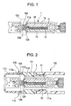
- Fig. 1 is a plan view of the circuit board according to the embodiment of the present invention.
- Fig. 2 is a plan view of the circuit board built in a wiper lever partially cut away. Referring to Fig. 2 , a casing 110 which serves as an external wall of the wiper lever is illustrated in cross-sectional view and the circuit board 1 is illustrated in plan view.
- the circuit board has four kinds of circuit patterns 10 to 13 formed on at least one surface (principal surface) of a main body (hereinafter, referred to as a "board main body") 1a of the circuit board such that the circuit patterns 10 to 13 are isolated from each other.
- An electronic component (not shown) is mounted on each of the circuit patterns 10 to 13.
- the two circuit patterns 10 and 13 are arranged so as to surround the two circuit patterns 11 and 12 extending between the patterns 10 and 13.
- the circuit patterns 11 and 12 extend in the middle of the board and the circuit patterns 10 and 13 are arranged so as to be closer to sides of the board than the circuit patterns 11 and 12.
- antistatic components are provided for the circuit patterns 10 and 13, respectively.
- the circuit patterns 10 and 13 include angular parts 10A and 13A each shaped in a series of rectangles, respectively.
- the angular parts 10A and 13A are positioned in an area 105, surrounded by a dashed line in Fig. 1 , corresponding to a static electricity entrance.
- the other circuit patterns 11 and 12 include semicircular end parts 11A and 12A which serve as non-angular parts, respectively.
- the semicircular parts 11A and 12A are positioned in the area 105, indicated by the dashed line in Fig. 1 , corresponding to the static electricity entrance.
- the slide switch 111 is rotatably attached to one end of the wiper lever casing 110.
- the slide switch 111 includes a connecting portion 111a inserted in an opening in the end of the wiper lever casing 110.
- the connecting portion 111a has an outer diameter slightly smaller than the inner diameter of the wiper lever casing 110.
- the connecting portion 111a is sized so as to be inserted from the opening of the end portion of the wiper lever casing 110 into the casing 110 as far as it will go. Accordingly, the overlap between the external wall of the wiper lever casing 110 and the connecting portion 111a is long to provide a structure that makes the entrance of static electricity through a gap between the external wall of the wiper lever casing 110 and the connecting portion 111a difficult.
- the connecting portion 111a of the slide switch 111 is permitted to be long, a structure that prevents the entrance of static electricity can be provided.
- a rotary operating member 113 is rotatably attached to one end of the slide switch 111.
- the rotary operating member 113 includes a connecting portion 113a rotatably attached to a stepped portion 111b formed on the inner wall of the open end of the slide switch 111.
- the overlap between the stepped portion 111b and the connecting portion 113a is restricted to a slight extent for lack of space.
- a gap 112 is provided between the stepped portion 111b and the connecting portion 113a. Since the rotary operating member 113 is a component directly touched by a driver, the gap 112 positioned in the vicinity of the rotary operating member 113 serves as a static electricity entrance as viewed from the circuit board 1.
- a casing constituting the external wall of the slide switch 111 (including the rotary operating member 113) directly touched by the driver typically includes a plastic molding made of a nonmetal material.
- the driver touches the rotary operating member 113 therefore, static electricity entered through the gap 112 into the casing may be discharged in the circuit patterns. Accordingly, the area 105 indicated by the dashed line of Fig. 1 corresponds to the static electricity entrance.
- an antistatic component is provided for each of the circuit patterns 10 and 13.
- the angular parts 10A and 13A for causing a discharge of static electricity are provided for the circuit patterns 10 and 13, respectively.
- Parts of the other circuit patterns 11 and 12 in the vicinity of the static electricity entrance are formed as non-angular parts (the semicircular end parts 11A and 12A). Consequently, there is a predominant probability that static electricity entered through the static electricity entrance shown by the dashed line flows toward the angular parts 10A and 13A of the circuit patterns 10 and 13, while the non-angular parts of the other circuit patterns 11 and 12 are also positioned in the vicinity of the static electricity entrance.
- the other circuit patterns 11 and 12 arranged in the vicinity of the static electricity entrance include no angular part. Accordingly, the non-angular parts of the circuit patterns 11 and 12 and the angular parts 10A and 13A of the circuit patterns 10 and 13 are arranged in the vicinity of the static electricity entrance. Since the circuit patterns 11 and 12 are intentionally formed so as not to have a shape causing a discharge of static electricity, the circuit patterns 11 and 12 each have a low probability that static electricity entered through the static electricity entrance is discharged to flow into the circuit pattern. It is therefore unnecessary to provide an antistatic component (not shown) that protects an electronic component, such as an IC, connected to a circuit pattern from static electricity for each of the circuit patterns 11 and 12.
- circuit patterns 11 and 12 are surrounded by the circuit patterns 10 and 13 which are made proof against static electricity (or in which measures to prevent instantaneous overcurrent are taken), the circuit patterns 10 and 13 function as protective patterns, thus improving the resistance of the circuit patterns 11 and 12 to external electrical noise including static electricity.
- circuit patterns 10 to 13 arranged in the circuit board 1 namely, the circuit patterns 10 and 13 have the angular parts 10A and 13A that induce a discharge of static electricity, thereby remarkably reducing a probability that static electricity flows into the other circuit patterns 11 and 12.
- antistatic components can be omitted from the circuit patterns 11 and 12.
- the number of antistatic components used can be reduced, thus reducing costs.
- the above description relates to the embodiment in which the circuit board 1 according to the embodiment of the present invention is applied to the wiper lever in the car.
- the present invention can be similarly applied to other electronic devices having a structure in which a circuit board is built in a casing and static electricity may enter through a gap in the casing.
- the present invention can be applied to other circuit board assemblies including a circuit board and electrical components mounted on the board. In each circuit board assembly, only a pattern having an angular part is made proof against static electricity, thus reducing costs.
- each of the angular parts 10A and 13A of the circuit patterns 10 and 13 is shaped in a series of rectangles, as shown in Fig. 1 .
- the shape of such a circuit pattern is not limited to the above shape. So long as each angular part easily induces a discharge of static electricity, the angular part may have any shape. For example, when each angular part is sawtoothed such that the part is shaped in a series of triangles, similar functions can be achieved.
- the present invention is applicable to a static electricity measure for a circuit board mounted on an electronic device.
Landscapes
- Engineering & Computer Science (AREA)
- Microelectronics & Electronic Packaging (AREA)
- Elimination Of Static Electricity (AREA)
- Structure Of Printed Boards (AREA)
- Switch Cases, Indication, And Locking (AREA)
Abstract
A circuit board (1) received in a casing (110) having a gap (112) includes a board main body (1a), a plurality of circuit patterns (10, 11, 12, 13) arranged on the principal surface of the board main body (1a) such that the patterns are isolated from each other, and angular parts (10A, 13A) that induce a discharge of static electricity, the angular parts being included in some patterns (10, 13) of the patterns (10, 11, 12, 13) such that the angular parts are arranged in an area (105) facing the gap (112) of the casing (110). In the circuit board (1), the circuit patterns (10, 13) with the angular parts (10A, 13A) are arranged so as to surround the other circuit patterns (11, 12). Each of the angular parts (10A, 13A) is shaped in a series of rectangles or triangles.
Description
- The present invention relates to a circuit board mounted on an electronic device or a component constituting an electronic device, and in particular, relates to a static-proof circuit board and circuit board assembly.
- Hitherto, circuit boards mounted on electronic devices are made proof against static electricity in order to protect circuit components. When a discharge of static electricity occurs in the vicinity of a circuit board provided with a plurality of circuit patterns, it is difficult to specify through which circuit pattern discharge current flows to the ground. Accordingly, for making electronic components, such as an integrated circuit (IC), connected to the circuit patterns proof against static electricity, an antistatic component (i.e., a component that dissipates static electricity) is provided for each of the circuit patterns.
Fig. 3 is a plan view of acircuit board 100 built in a wiper switch in a car. Thecircuit board 100 is provided with four kinds ofcircuit patterns 101 to 104. An antistatic component (not shown) is provided for each of thesecircuit patterns 101 to 104. - Discharges due to static electricity include a discharge of charge accumulated in or on a human body. For example, assuming that a person gets on a car in a dry season, charge is generated by the friction between clothes of the person and a sheet, so that the charge is accumulated on the clothes. For example, when a driver operates a slide switch for wiper time control disposed in a wiper lever, the charge (static electricity) accumulated on the clothes of the driver may be discharged through a slight gap in the slide switch to a circuit pattern in a circuit board (refer to
Fig. 3 ) received in the wiper lever. -
Fig. 4 is a perspective view illustrating a wiper lever in a car. Referring toFig. 4 , aslide switch 111 for wiper time control is disposed in an end portion of awiper lever 110. Charge accumulated on clothes of a driver flows through any gap between a main body of thelever 110 and theslide switch 111, i.e., a gap adjacent to the proximal end of thewiper lever 110 or agap 112 adjacent to the distal end thereof, thus causing a discharge of the charge in a circuit board built in thewiper lever 110. In this case, anarea 105 surrounded by a dashed line in thecircuit board 100 shown inFig. 3 corresponds to the position of theslide switch 111 in thewiper lever 110. This area serves as an entrance which static electricity enters through thegap 112 between the lever main body and theslide switch 111. The static electricity entered the static-electricity entrance of thecircuit board 100 flows through any of thecircuit patterns 101 to 104 and is then removed by the antistatic component provided for the circuit pattern which has undergone the discharge. - Related arts are disclosed in Japanese Unexamined Utility Model Registration Application Publication No.
5-076071 9-045194 2004-134453 - However, providing the antistatic components for all of the circuit patterns arranged in the circuit board results in an increase in the number of components. Disadvantageously, this leads to increased costs. For example, since the
circuit board 100 shown inFig. 3 has the four kinds ofcircuit patterns 101 to 104, at least four antistatic components are needed. - The present invention has been made in consideration of the above-described disadvantages. The present invention provides a circuit board and circuit board assembly which are capable of reliably protecting electronic components, such as an IC, connected to circuit patterns from static electricity while achieving a reduction in the number of antistatic components used.
- An aspect of the present invention provides a circuit board received in a casing having a gap, the circuit board including a board main body, a plurality of patterns arranged on the principal surface of the board main body such that the patterns are isolated from each other, and angular parts that induce a discharge of static electricity, the angular parts being included in some of the patterns such that the angular parts are arranged in an area facing the gap in the casing.
- With this structure, the angular parts that induce a discharge of static electricity are included in some of the patterns arranged in the circuit board, thus remarkably reducing a probability that static electricity flows into the other patterns. Accordingly, antistatic components can be omitted from the other patterns. Consequently, a reduction in the number of antistatic components can be achieved, thus reducing costs.
- In the circuit board, the patterns with the angular parts may be arranged so as to surround the patterns with no angular parts. Since the patterns which are made proof against static electricity (or in which measures to prevent instantaneous overcurrent are taken) surround the other patterns, the patterns made proof against static electricity function as protective patterns, thus improving the resistance of the other patterns to external electrical noise including static electricity.
- In the circuit board, each of the angular parts may be shaped in a series of rectangles or triangles.
- Another aspect of the present invention provides a circuit board assembly received in a casing having a gap, the circuit board assembly including a board main body and a plurality of patterns arranged on the principal surface of the board main body such that the patterns are isolated from each other. The patterns include angled patterns with angular parts that induce a discharge of static electricity and non-angled patterns with no angular parts, the angular parts being included in the angled patterns such that the angular parts are arranged in an area facing the gap in the casing. The angled patterns are arranged so as to surround the non-angled patterns. Only the angled patterns are made proof against static electricity.
- With this structure, only the patterns with the angular parts are made proof against static electricity, thus reducing costs.
- The circuit board and the circuit board assembly according to the aspects of the present invention can reliably protect electronic components, such as an IC, connected to the circuit patterns from static electricity while achieving a reduction in the number of antistatic components used.
-
-
Fig. 1 is a plan view of a circuit board according to an embodiment of the present invention; -
Fig. 2 is a diagram illustrating the circuit board ofFig. 1 built in a wiper lever. -
Fig. 3 is a plan view of a conventional circuit board; and -
Fig. 4 is a perspective view of a wiper lever in a car. - An embodiment of the present invention will be described in detail below with reference to the accompanying drawings.
- A circuit board according to an embodiment of the present invention is built in a casing which serves as a housing of a wiper lever in a car in a manner similar to the
circuit board 100 shown inFig. 3 . -
Fig. 1 is a plan view of the circuit board according to the embodiment of the present invention.Fig. 2 is a plan view of the circuit board built in a wiper lever partially cut away. Referring toFig. 2 , acasing 110 which serves as an external wall of the wiper lever is illustrated in cross-sectional view and thecircuit board 1 is illustrated in plan view. - Referring to
Fig. 1 , the circuit board, indicated at 1, has four kinds ofcircuit patterns 10 to 13 formed on at least one surface (principal surface) of a main body (hereinafter, referred to as a "board main body") 1a of the circuit board such that thecircuit patterns 10 to 13 are isolated from each other. An electronic component (not shown) is mounted on each of thecircuit patterns 10 to 13. In the arrangement of the patterns inFig. 1 , the twocircuit patterns circuit patterns patterns circuit patterns circuit patterns circuit patterns circuit patterns circuit patterns - The
circuit patterns angular parts angular parts area 105, surrounded by a dashed line inFig. 1 , corresponding to a static electricity entrance. Theother circuit patterns semicircular end parts semicircular parts area 105, indicated by the dashed line inFig. 1 , corresponding to the static electricity entrance. - Referring to
Fig. 2 , theslide switch 111 is rotatably attached to one end of thewiper lever casing 110. Theslide switch 111 includes a connectingportion 111a inserted in an opening in the end of thewiper lever casing 110. The connectingportion 111a has an outer diameter slightly smaller than the inner diameter of thewiper lever casing 110. The connectingportion 111a is sized so as to be inserted from the opening of the end portion of thewiper lever casing 110 into thecasing 110 as far as it will go. Accordingly, the overlap between the external wall of thewiper lever casing 110 and the connectingportion 111a is long to provide a structure that makes the entrance of static electricity through a gap between the external wall of thewiper lever casing 110 and the connectingportion 111a difficult. When the connectingportion 111a of theslide switch 111 is permitted to be long, a structure that prevents the entrance of static electricity can be provided. - On the other hand, a
rotary operating member 113 is rotatably attached to one end of theslide switch 111. Therotary operating member 113 includes a connectingportion 113a rotatably attached to a steppedportion 111b formed on the inner wall of the open end of theslide switch 111. The overlap between the steppedportion 111b and the connectingportion 113a is restricted to a slight extent for lack of space. Agap 112 is provided between the steppedportion 111b and the connectingportion 113a. Since therotary operating member 113 is a component directly touched by a driver, thegap 112 positioned in the vicinity of therotary operating member 113 serves as a static electricity entrance as viewed from thecircuit board 1. A casing constituting the external wall of the slide switch 111 (including the rotary operating member 113) directly touched by the driver typically includes a plastic molding made of a nonmetal material. When the driver touches therotary operating member 113, therefore, static electricity entered through thegap 112 into the casing may be discharged in the circuit patterns. Accordingly, thearea 105 indicated by the dashed line ofFig. 1 corresponds to the static electricity entrance. - As described above, in the present embodiment, an antistatic component is provided for each of the
circuit patterns angular parts circuit patterns other circuit patterns semicircular end parts angular parts circuit patterns other circuit patterns - The
other circuit patterns circuit patterns angular parts circuit patterns circuit patterns circuit patterns circuit patterns - Furthermore, since the
circuit patterns circuit patterns circuit patterns circuit patterns - Irrespective of whether the
circuit patterns circuit patterns angular parts circuit patterns angular parts - As described above, according to the present embodiment, some of the
circuit patterns 10 to 13 arranged in thecircuit board 1, namely, thecircuit patterns angular parts other circuit patterns circuit patterns - The above description relates to the embodiment in which the
circuit board 1 according to the embodiment of the present invention is applied to the wiper lever in the car. In addition to the wiper lever in the car, the present invention can be similarly applied to other electronic devices having a structure in which a circuit board is built in a casing and static electricity may enter through a gap in the casing. Furthermore, in addition to a circuit board assembly incorporated in the wiper lever in the car, the present invention can be applied to other circuit board assemblies including a circuit board and electrical components mounted on the board. In each circuit board assembly, only a pattern having an angular part is made proof against static electricity, thus reducing costs. - In the above-described embodiment, each of the
angular parts circuit patterns Fig. 1 . The shape of such a circuit pattern is not limited to the above shape. So long as each angular part easily induces a discharge of static electricity, the angular part may have any shape. For example, when each angular part is sawtoothed such that the part is shaped in a series of triangles, similar functions can be achieved. - The present invention is applicable to a static electricity measure for a circuit board mounted on an electronic device.
Claims (4)
- A circuit board (1) received in a casing (110) having a gap (112), comprising:a board main body (1a);a plurality of patterns (10, 11, 12, 13) arranged on the principal surface of the board main body (1a) such that the patterns are isolated from each other; andangular parts (10A, 13A) that induce a discharge of static electricity, the angular parts being included in some patterns (10, 13) of the patterns (10, 11, 12, 13) such that the angular parts are arranged in an area (105) facing the gap (112) in the casing (110).
- The circuit board according to Claim 1, wherein the patterns (10, 13) with the angular parts (10A, 13A) are arranged so as to surround the patterns (11, 12) with no angular parts.
- The circuit board according to Claim 1 or 2, wherein each of the angular parts (10A, 13A) is shaped in a series of rectangles or triangles.
- A circuit board assembly received in, a casing (110) having a gap (112), comprising:a board main body (1a); anda plurality of patterns (10, 11, 12, 13) arranged on the principal surface of the board main body (1a) such that the patterns are isolated from each other, whereinthe patterns (10, 11, 12, 13) include angled patterns (10, 13) with angular parts (10A, 13A) that induce a discharge of static electricity and non-angled patterns (11, 12) with no angular parts, the angular parts being included in the angled patterns such that the angular parts are arranged in an area (105) facing the gap (112) in the casing (110),the angled patterns (10, 13) are arranged so as to surround the non-angled patterns (11, 12), andonly the angled patterns (10, 13) are made proof against static electricity.
Applications Claiming Priority (1)
| Application Number | Priority Date | Filing Date | Title |
|---|---|---|---|
| JP2009043779A JP2010199376A (en) | 2009-02-26 | 2009-02-26 | Circuit board and circuit board assembly |
Publications (1)
| Publication Number | Publication Date |
|---|---|
| EP2224793A1 true EP2224793A1 (en) | 2010-09-01 |
Family
ID=42112297
Family Applications (1)
| Application Number | Title | Priority Date | Filing Date |
|---|---|---|---|
| EP10151320A Withdrawn EP2224793A1 (en) | 2009-02-26 | 2010-01-21 | Circuit board and circuit board assembly |
Country Status (3)
| Country | Link |
|---|---|
| EP (1) | EP2224793A1 (en) |
| JP (1) | JP2010199376A (en) |
| CN (1) | CN101820723A (en) |
Citations (5)
| Publication number | Priority date | Publication date | Assignee | Title |
|---|---|---|---|---|
| US4667266A (en) * | 1985-03-09 | 1987-05-19 | Kabushiki Kaisha Toshiba | Printed-circuit board with protection against static discharge damage |
| JPH0945194A (en) | 1995-08-01 | 1997-02-14 | Omron Corp | Penetration type proximity sensor |
| JP2004134453A (en) | 2002-10-08 | 2004-04-30 | Funai Electric Co Ltd | Circuit board having static electricity protective pattern |
| US20070115640A1 (en) * | 2005-11-15 | 2007-05-24 | Brother Kogyo Kabushiki Kaisha | Electronic apparatus |
| US20080158766A1 (en) * | 2006-12-28 | 2008-07-03 | Fuji Xerox Co., Ltd. | Circuit board and electronic component |
-
2009
- 2009-02-26 JP JP2009043779A patent/JP2010199376A/en not_active Withdrawn
-
2010
- 2010-01-21 EP EP10151320A patent/EP2224793A1/en not_active Withdrawn
- 2010-02-24 CN CN201010125242A patent/CN101820723A/en active Pending
Patent Citations (5)
| Publication number | Priority date | Publication date | Assignee | Title |
|---|---|---|---|---|
| US4667266A (en) * | 1985-03-09 | 1987-05-19 | Kabushiki Kaisha Toshiba | Printed-circuit board with protection against static discharge damage |
| JPH0945194A (en) | 1995-08-01 | 1997-02-14 | Omron Corp | Penetration type proximity sensor |
| JP2004134453A (en) | 2002-10-08 | 2004-04-30 | Funai Electric Co Ltd | Circuit board having static electricity protective pattern |
| US20070115640A1 (en) * | 2005-11-15 | 2007-05-24 | Brother Kogyo Kabushiki Kaisha | Electronic apparatus |
| US20080158766A1 (en) * | 2006-12-28 | 2008-07-03 | Fuji Xerox Co., Ltd. | Circuit board and electronic component |
Also Published As
| Publication number | Publication date |
|---|---|
| CN101820723A (en) | 2010-09-01 |
| JP2010199376A (en) | 2010-09-09 |
Similar Documents
| Publication | Publication Date | Title |
|---|---|---|
| EP1786251B1 (en) | Electronic control unit and waterproof case | |
| WO2005065097A3 (en) | Internally shielded energy conditioner | |
| DE102005025021A1 (en) | switching element | |
| US20110241830A1 (en) | Portable transmitter | |
| US20140021025A1 (en) | Flat motor vehicle key | |
| JP3690519B2 (en) | Circuit board with electrostatic protection pattern | |
| JP6213058B2 (en) | Operating device | |
| JP4624271B2 (en) | Antistatic structure of pushbutton switch device in electronic equipment | |
| JP2010199376A (en) | Circuit board and circuit board assembly | |
| EP2008839B1 (en) | Air-conditioning control unit | |
| JP2009026503A (en) | Electronics | |
| US20070253127A1 (en) | Electrostatic discharge protection structure of electronic device | |
| CN211788737U (en) | Key structure, electric control box assembly and air conditioner | |
| JP4407266B2 (en) | 2-wire proximity switch and gaming machine | |
| US6064292A (en) | Electrostatic discharge protected fuse and fuse holder | |
| CN101714482B (en) | Electronic trip | |
| US6080946A (en) | Dip switch with enhanced anti-EMI performance | |
| JP4035097B2 (en) | Outdoor unit of separate air conditioner | |
| JP2591140B2 (en) | Printed board | |
| JP4907915B2 (en) | Cable bushing for distribution box | |
| JPH0119775Y2 (en) | ||
| JP3864804B2 (en) | LCD display | |
| CN211670875U (en) | 5G terminal fingerprint identification module and terminal equipment | |
| US20030231470A1 (en) | Electrical device, in particular for a motor vehicle | |
| JP3000361U (en) | Structure of electrical equipment case |
Legal Events
| Date | Code | Title | Description |
|---|---|---|---|
| PUAI | Public reference made under article 153(3) epc to a published international application that has entered the european phase |
Free format text: ORIGINAL CODE: 0009012 |
|
| AK | Designated contracting states |
Kind code of ref document: A1 Designated state(s): AT BE BG CH CY CZ DE DK EE ES FI FR GB GR HR HU IE IS IT LI LT LU LV MC MK MT NL NO PL PT RO SE SI SK SM TR |
|
| 17P | Request for examination filed |
Effective date: 20110225 |
|
| STAA | Information on the status of an ep patent application or granted ep patent |
Free format text: STATUS: THE APPLICATION HAS BEEN WITHDRAWN |
|
| 18W | Application withdrawn |
Effective date: 20111005 |