EP2220562B1 - Method and apparatus for lowering i/o power of a computer system and computer system - Google Patents
Method and apparatus for lowering i/o power of a computer system and computer system Download PDFInfo
- Publication number
- EP2220562B1 EP2220562B1 EP08850030.1A EP08850030A EP2220562B1 EP 2220562 B1 EP2220562 B1 EP 2220562B1 EP 08850030 A EP08850030 A EP 08850030A EP 2220562 B1 EP2220562 B1 EP 2220562B1
- Authority
- EP
- European Patent Office
- Prior art keywords
- bus
- data
- encoding
- power
- computer system
- Prior art date
- Legal status (The legal status is an assumption and is not a legal conclusion. Google has not performed a legal analysis and makes no representation as to the accuracy of the status listed.)
- Active
Links
Images



Classifications
-
- G—PHYSICS
- G06—COMPUTING OR CALCULATING; COUNTING
- G06F—ELECTRIC DIGITAL DATA PROCESSING
- G06F13/00—Interconnection of, or transfer of information or other signals between, memories, input/output devices or central processing units
- G06F13/38—Information transfer, e.g. on bus
- G06F13/42—Bus transfer protocol, e.g. handshake; Synchronisation
- G06F13/4282—Bus transfer protocol, e.g. handshake; Synchronisation on a serial bus, e.g. I2C bus, SPI bus
- G06F13/4286—Bus transfer protocol, e.g. handshake; Synchronisation on a serial bus, e.g. I2C bus, SPI bus using a handshaking protocol, e.g. RS232C link
-
- G—PHYSICS
- G06—COMPUTING OR CALCULATING; COUNTING
- G06F—ELECTRIC DIGITAL DATA PROCESSING
- G06F13/00—Interconnection of, or transfer of information or other signals between, memories, input/output devices or central processing units
- G06F13/14—Handling requests for interconnection or transfer
-
- G—PHYSICS
- G06—COMPUTING OR CALCULATING; COUNTING
- G06F—ELECTRIC DIGITAL DATA PROCESSING
- G06F13/00—Interconnection of, or transfer of information or other signals between, memories, input/output devices or central processing units
- G06F13/38—Information transfer, e.g. on bus
- G06F13/42—Bus transfer protocol, e.g. handshake; Synchronisation
-
- Y—GENERAL TAGGING OF NEW TECHNOLOGICAL DEVELOPMENTS; GENERAL TAGGING OF CROSS-SECTIONAL TECHNOLOGIES SPANNING OVER SEVERAL SECTIONS OF THE IPC; TECHNICAL SUBJECTS COVERED BY FORMER USPC CROSS-REFERENCE ART COLLECTIONS [XRACs] AND DIGESTS
- Y02—TECHNOLOGIES OR APPLICATIONS FOR MITIGATION OR ADAPTATION AGAINST CLIMATE CHANGE
- Y02D—CLIMATE CHANGE MITIGATION TECHNOLOGIES IN INFORMATION AND COMMUNICATION TECHNOLOGIES [ICT], I.E. INFORMATION AND COMMUNICATION TECHNOLOGIES AIMING AT THE REDUCTION OF THEIR OWN ENERGY USE
- Y02D10/00—Energy efficient computing, e.g. low power processors, power management or thermal management
Definitions
- the present invention relates to computer technology, more particularly to technology of lowering I/O power of a computer system.
- Power of a computer system includes core power and I/O (Input/Output) power.
- I/O Input/Output
- methods for lowering power of the computer system for example:
- a specific example is a power management system of Intel DBS (Demand Based Switching), which has a logic for adjusting core power. It can adjust core voltage based on CPU's workload.
- Intel DBS Demand Based Switching
- the detailed description about Intel DBS can be seen in the Intel white paper: Addressing Power and Thermal Challenges in the Datacenter, www.intel.com/products/services/intelsolutionservices/success/techdocs/wp/therm al.pdf .
- the power management system of Intel DBS is mainly focused on the processor itself and doesn't lower I/O power effectively.
- WO2006/027742 describes a module comprising a bus invert encoder for determining whether a set of data bits should be inverted prior to transmission over a communication bus.
- the bus invert encoder produces a bus invert signal BI which controls a selective inversion means, for example a multiplexer.
- a partial fault detection encoder determines one or more temporary check bits from the set of data bits, substantially in parallel with the bus invert encoder. Thus, the one or more temporary check bits are determined based on the assumption that the set of data bits are to be transmitted without inversion from the selective inversion means.
- a logic unit is provided for correcting the one or more temporary check bits, if necessary, based on the bus invert signal produced by the bus invert encoder.
- the present invention provides a method and an apparatus for lowering I/O power of a computer system and a computer system.
- a method for lowering I/O power of a computer system comprising: buffering a plurality of ways of data to be sent to a bus; encoding each of said plurality of ways of data buffered from n bits to n+m bits based on an encoding rule, wherein n and m are both an integer larger than or equal to 1, said encoding rule is used to lower code switching frequency; and sending said plurality of ways of data encoded to said bus, wherein said encoding rule comprises a code book mapping an n bit data space with an n+m bit data space, in which all codes of said n bit data space are mapped with codes of said n+m bit data space one to one.
- a computer system comprising: a CPU; an I/O device; a bus configured to transfer data between CPU and I/O device; and an apparatus for lowering I/O power of a computer system, the apparatus comprising logic operable to perform the above method.
- the present invention will make efforts to lower I/O power through lowering switching frequency. Specifically, since system clock holds constant generally, the present invention will lower I/O power through lowering switching action.
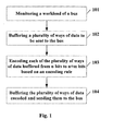
- Fig. 1 is a flowchart showing a method for lowering I/O power of a computer system according to an embodiment of the present invention. Before describing the embodiment of the method of Fig. 1 , the principle of lowering I/O power through lowering switching frequency through temporarily encoding data to be sent to a bus is explained in conjunction with Fig. 2 and Table 1.
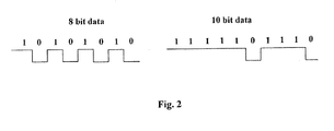
- Fig. 2 is a contrastive figure of switching times showing the times of switching action of 8 bit data and 10 bit data according to the embodiment of the present invention.
- Fig. 2 for an 8 bit data 10101010, its switching times is 7, and for a 10 bit data 1111101110 corresponding to the 8 bit data, its switching times is 3.
- the 8 bit data is encoded to the 10 bit data, the maximum switching times is lowered from 7 to 3, and switching frequency is lowered, and I/O power is lowered consequently.
- Table 1 shows a code book mapping an 8 bit data space with a 10 bit data space and the switching times.
- the total switching times of the 8 bit data space is 896.
- this number 896 is only used to statistically denote power performance gain in an average meaning, and it is possible to become higher or lower when an input data collection is provided with other characters.
- the total switching times of the 10 bit data space is 654, and this number is the optimum value of the 10 bit data space, because codes with the switching times less than or equal to 2 are all included in this code book, and a part of the 10 bit codes with the switching times equal to 3 are included in Table 1.
- the total switching times can be lowered from 896 to 654, and I/O power can be lowered 27% consequently.
- I/O power can be lowered about 20% if the spending is deducted.
- any n bits can be also encoded to n+m bits based on the above-mentioned encoding rule, wherein n and m are both an integer larger than or equal to 1, and I/O power of a computer system is lowered through lowering switching frequency consequently.
- Fig. 1 is a flowchart showing a method for lowering I/O power of a computer system according to an embodiment of the present invention.
- a workload of a bus of the computer system is monitored.
- a bus monitor or any module or technology as known by those skilled in the art can be used to monitor the workload of the bus, for example, the data queuing situation in a register is read continuously through an operating system of a computer, thereby, information related to the working situation of the bus is obtained to monitor the workload of the bus.
- the workload of the bus is obtained instantly when data are required to be transferred between a CPU and an I/O device, and the present invention has no limitation to this, if only the workload of the bus can be obtained when needed.
- the I/O device mentioned herein includes but not limits to: a display device, a system memory such as a read-only memory and a random access memory etc, a hard disk, a CD-ROM, an input device such as a mouse and a keyboard etc, a network device such as a router etc, and other devices as known in the art or developed in the future, and the present invention has no limitation to the I/O device, and any device inputted/outputted with CPU through the bus can be the I/O device herein.
- step of monitoring the workload of the bus is only an optional step of the embodiment, the purpose of which is to balance the relation between efficiency of inputting/outputting data with the bus and I/O power better, and the bus can also not be monitored in this embodiment, and the following step is performed directly.
- a plurality of ways of data to be sent to the bus are buffered.
- the plurality of ways of data to be sent to the bus can be buffered by using any memory of the computer system, for example, a shift register is used to buffer the data, and the present invention has no limitation to this.
- each of the plurality of ways of data buffered at Step 102 are encoded from n bits to n+m bits based on an encoding rule, wherein n and m are both an integer larger than or equal to 1.
- the encoding rule herein is namely the above-mentioned encoding rule described in conjunction with Fig. 2 and Table 1, which is used to lower code switching frequency.
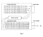
- Fig. 3 is an example showing encoding data from 8 bits to 10 bits according to the embodiment of the present invention.
- the 4 ways of data to be sent to the bus are buffered in an original data buffer in a format of 8 bits per each way, and then the plurality of ways of 8 bit data are encoded to 10 bit data respectively by using a shared encoder for the 4 ways of data, and the 10 bit data encoded are buffered in an encoded data buffer.
- the plurality of ways of the 8 bit data can be encoded to the 10 bit data corresponding to it by the shared encoder by using the code book pre-stored as shown in Table 1.
- Table 1 code book pre-stored
- Fig. 4 is another example showing encoding data from 8 bits to 10 bits according to the embodiment of the present invention.
- the plurality of ways of data are provided with their own encoders, and the encoding process is same with the above-mentioned example of Fig. 3 , which is appropriately omitted herein.
- the present invention is not limited to this, and the present invention can provide any encoder for any plurality of ways of data based on a practical need, if only each of the plurality of ways of the 8 bit data can be encoded to the 10 bit data.
- the present invention is not limited to this, and the present invention can encode any n bit data to n+m data, if only switching frequency can be lowered based on the above-mentioned encoding rule.
- a threshold can be defined at the step of encoding the plurality of ways of data buffered of Step 103, and this threshold can be the workload monitored at Step 101, for example, this threshold is defined as 0.6, that is to say, the bus is defined busy when the workload of the bus is larger than or equal to 60%, and the bus is defined not busy when the workload of the bus is less than 60%. It should be understood that, this threshold 0.6 is just an example, the threshold of busy and not busy of the bus can be defined as any value between 0 and 1 based on a practical instance, and the present invention has no limitation to the threshold definition.
- the bus when it is monitored that the workload of the bus is below the above-mentioned threshold such as 0.6, the bus is namely not busy, the plurality of ways of data to be sent to the bus buffered are encoded from n bits to n+m bits, and the present invention has no limitation to this.
- the workload of the bus can be defined as some ranges such as 80-100%, 60-80%, 40-60%, 20-40%, 0-20%, and different encoding rules are selected for different levels of the workload respectively. For example, if the workload of the bus is monitored in 80-100% at Step 101, the encoding rule from 8 bits to 10 bits is selected; if the workload of the bus is monitored in 60-80% at Step 101, the encoding rule from 8 bits to 12 bits is selected; if the workload of the bus is monitored in 40-60% at Step 101, the encoding rule from 8 bits to 14 bits is selected; if the workload of the bus is monitored in 20-40% at Step 101, the encoding rule from 8 bits to 16 bits is selected; if the workload of the bus is monitored in 0-20% at Step 101, the encoding rule from 8 bits to 18 bits is selected. It should be understood that, the above-mentioned ranges of the workload and the corresponding encoding rules are just examples, and the present invention can define any range of
- the plurality of ways of data encoded are buffered, data buffered are sent to the bus, and data encoded are sent to the CPU or the I/O device through the bus.
- the plurality of ways of data to be sent to the bus can be buffered by using any memory of the computer system, for example, the shift register is used for buffering, and the present invention has no limitation to this.
- the encoding rule can also be sent to a CPU side I/O controller and/or an I/O device side I/O controller when it is monitored that the workload of the bus is below a threshold at Step 101.
- the corresponding encoder is controlled to perform encoding at Step 103 by the CPU side I/O controller and/or the I/O device side I/O controller based on the encoding rule received.
- the method of the embodiment further comprises a step of decoding the n+m bit data encoded into n bit data based on the above-mentioned encoding rule, and the decoding process is opposite to the above-mentioned encoding process, that is to say, firstly, the plurality of ways of the n+m bit data encoded from the bus are buffered; next, the n+m bit data buffered are decoded into the n bit data based on the above-mentioned encoding rule; next, the plurality of ways of the n bit data decoded are buffered; at last, the n bit data buffered are sent to the CPU or the I/O device.
- the above-mentioned encoding/decoding can be implemented through hardware such as an IC etc.
- the encoder/decoder can be integrated into the computer system directly, or the encoder/decoder can also be integrated into I/O controller of the computer system.
- the encoding/decoding can also be implemented through software. So-called implementation through software means that data are outputted after being encoded/decoded through a software program when data is to be outputted by the CPU. The present invention has no limitation to this, if only the encoding/decoding can be performed between the n bit data and the n+m bit data.
- the workload of the bus is monitored at Step 101 before the encoding at Step 103
- the monitoring process at Step 101 is optional, the purpose of which is to balance the relation between efficiency of inputting/outputting data and I/O power.
- the bus can also not be monitored, the plurality of ways of data to be sent to the bus are buffered directly, and then the encoding is performed.
- I/O power can be lowered effectively based on the workload level of the bus of the computer system. Thereby, the energy consumption is saved infinitely.
- An 8-10 bit encoding/decoding system is implemented in a simulation system by the inventor of the present invention. Specifically, a hardware design of the encoder/decoder is completed by the inventor.
- FIG. 5 is a block diagram showing an apparatus for lowering I/O power of a computer system according to another embodiment of the present invention.
- the present embodiment will be described in conjunction with Fig. 5 .
- the description of which will be appropriately omitted.
- the apparatus 600 for lowering I/O power of a computer system of the embodiment comprises a bus monitor 601 configured to monitor a workload of the bus of the computer system.
- a bus monitor 601 configured to monitor a workload of the bus of the computer system.
- any module or technology as known by those skilled in the art can be used as the bus monitor 601 to monitor the workload of the bus, for example, the data queuing situation in a register is read continuously through an operating system of a computer, thereby, information related to the working situation of the bus is obtained to monitor the workload of the bus.
- the workload of the bus is obtained by the bus monitor 601 instantly when data are required to be transferred between a CPU 701 and an I/O device 800, and the present invention has no limitation to this, if only the workload of the bus can be obtained when needed.
- the bus monitor 601 configured to monitor the workload of the bus is only an optional unit of the apparatus 600 of this embodiment, the purpose of which is to balance the relation between efficiency of inputting/outputting data with the bus and the I/O power better, and the bus can also not be monitored in this embodiment, that is to say, the apparatus 600 doesn't comprise the bus monitor 601.
- the I/O device 800 includes but not limits to: a display device, a system memory such as a read-only memory and a random access memory etc, a hard disk, a CD-ROM, an input device such as a mouse and a keyboard etc, a network device such as a router etc, and other devices as known in the art or developed in the future, and the present invention has no limitation to the I/O device, and any device inputted/outputted with CPU 701 through the bus can be the I/O device 800 herein.
- the apparatus 600 for lowering I/O power of a computer system of the embodiment also comprises an original data buffer 610 and/or 630 configured to buffer a plurality of ways of data to be sent to a bus.
- the original data buffer 610 and/or 630 can be any memory of the computer system such as a shift register, and the present invention has no limitation to this.
- encoding from n bits to n+m bits is performed by the apparatus 600 for lowering I/O power of a computer system of the embodiment, wherein n and m are both an integer larger than or equal to 1.
- the encoding rule from n bits to n+m bits can also be messaged to a CPU side I/O controller 605 and/or an I/O device side I/O controller 625.
- data buffered in the original data buffer 610 and/or 630 are encoded from n bits to n+m bits by the corresponding encoder/decoder 615 and/or 635, which is controlled by the CPU side I/O controller 605 and/or the I/O device side I/O controller 625.
- the encoding rule described herein is namely the above-mentioned encoding rule described in conjunction with Fig. 2 and Table 1, which is used to lower code switching frequency.
- a threshold can be defined for the encoder/decoder 615 and/or 635, which determines whether to encode the plurality of ways of data buffered or not, and this threshold can be the workload of the bus monitored by the bus monitor 601, for example, this threshold is defined as 0.6, that is to say, the bus is defined busy when the workload of the bus is larger than or equal to 60%, and the bus is defined not busy when the workload of the bus is less than 60%. It should be understood that, this threshold 0.6 is just an example, the threshold of busy and not busy of the bus can be defined as any value between 0 and 1 (namely larger than or equal to 0, and less than or equal to 1) based on a practical instance, and the present invention has no limitation to the threshold definition.
- the encoding process of the encoder/decoder 615 and/or 635 of the embodiment is similar with that of the above-mentioned embodiment described in conjunction with Fig. 3 and Fig. 4 , and the description of which is appropriately omitted herein.
- the plurality of ways of data encoded are buffered in an encoded data buffer 620 and/or 640. Then, data buffered in the encoded data buffer 620 and/or 640 are sent to the bus, and data encoded are sent to CPU 701 or I/O device 800 through the bus.
- the n+m bit data encoded from the bus are sent to CPU 701 or I/O device 800, the n+m bit data encoded are decoded into n bit data by the encoder/decoder 615 and/or 635 of the embodiment based on the above-mentioned encoding rule, and the decoding process is opposite to the encoding process described in conjunction with Fig. 3 and Fig.
- the plurality of ways of the n+m bit data encoded from the bus are buffered by using the encoded data buffer 620 and/or 640; next, the n+m bit data buffered are decoded into the n bit data based on the above-mentioned encoding rule; next, the plurality of ways of the n bit data decoded are buffered in the original data buffer 610 and/or 630; at last, the n bit data buffered are sent to CPU 701 or I/O device 800.
- the workload of the bus can be defined as some ranges such as 80-100%, 60-80%, 40-60%, 20-40%, 0-20%, and different encoding rules are selected for different levels of the workload respectively. For example, if the workload of the bus is monitored in 80-100% by the bus monitor 601, the encoding rule from 8 bits to 10 bits is selected; if the workload of the bus is monitored in 60-80% by the bus monitor 601, the encoding rule from 8 bits to 12 bits is selected; if the workload of the bus is monitored in 40-60% by the bus monitor 601, the encoding rule from 8 bits to 14 bits is selected; if the workload of the bus is monitored in 20-40% by the bus monitor 601, the encoding rule from 8 bits to 16 bits is selected; if the workload of the bus is monitored in 0-20% by the bus monitor 601, the encoding rule from 8 bits to 18 bits is selected. It should be understood that, the above-mentioned ranges of the workload and the corresponding encoding rules are just
- the above-mentioned encoder/decoder 615 and/or 635 can be implemented through hardware such as an IC etc.
- the encoder/decoder 615 and/or 635 can be integrated into the computer system directly, or the encoder/decoder 615 and/or 635 can also be integrated into I/O controller of the computer system.
- the encoder/decoder 615 and/or 635 can also be implemented through software. So-called implementation through a software means that data are outputted after being encoded/decoded through a software program when data is to be outputted by the CPU. The present invention has no limitation to this, if only the encoding/decoding can be performed between the n bit data and the n+m bit data.
- the bus monitor 601 is optional, the purpose of which is to balance the relation between efficiency of inputting/outputting data and I/O power, and the plurality of ways of data to be sent to the bus can also be buffered directly, and then the encoding is performed.
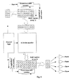
- an actual hardware circuit mainly includes 4 modules: a shift register array A, an 8-10 bit encoder, a shift register array B and a control logic.
- the 4 ways of data shown in Fig. 3 and Fig. 4 are taken as an example herein, the shift register array A is an 8 ⁇ 4 shift register matrix, and the shift register array B is a 10 ⁇ 4 shift register matrix.
- Each shift register can shift data rightwards or downwards, and the specific operation is controlled by the control logic and a shift counter.
- data (8 bits) sent from the CPU is controlled to be shifted rightwards by a transverse shift counter of the shift register array A.
- the transverse shift counter counts 8 data
- data are controlled to be shifted out downwards by a longitudinal shift counter, and data outputted is data to be encoded.
- data to be encoded received are transformed into codes of 10 bits and outputted to the shift register array B by the 8-10 bit encoder, and data are controlled to be shifted downwards in turn by a longitudinal shift counter.
- the longitudinal shift counter counts 4 data, data are controlled to be shifted out rightwards in turn by a transverse shift counter, and data shifted out are transferred to pins and sent to the bus.
- the hardware structure used for decoding is similar with the hardware structure of the encoding, it is just that, firstly, the 10 bit data to be decoded are buffered by using a 10 ⁇ 4 shift register matrix, then, data to be decoded are decoded into the 8 bit data, and then, data decoded are shifted and buffered in an 8x4 shift register matrix and outputted.
- the hardware structure shown in Fig. 6 is just an example of the apparatus 600 for lowering I/O power of a computer system of the embodiment, and the present invention is not limited to this, and the apparatus 600 for lowering I/O power of a computer system of the embodiment can be implemented through any combination of the hardware structure as known in the art or developed in the future, if only the plurality of ways of data can be encoded/decoded between n bits and n+m bits through the apparatus 600, thereby, switching frequency is lowered effectively, and I/O power is lowered moreover.
- I/O power can be lowered effectively based on the workload level of the bus of the computer system.
- the energy consumption is saved infinitely. For example, it is calculated through an 8-10 bit encoding/decoding system, which is implemented in an simulation system by the inventor of the present invention that, power caused by an encoding/decoding circuit added is about 5% of I/O power, and a net gain larger than 20% can be obtained finally compared with I/O power lowered of 27% obtained through the above-mentioned encoding.
- FIG. 7 is a block diagram showing a computer system according to another embodiment of the present invention. Next, the present embodiment will be described in conjunction with Fig. 7 . For those same parts as the above embodiments, the description of which will be appropriately omitted.
- the computer system 700 of the embodiment comprises: a central processing unit (CPU) 701; an I/O controller 708; a system bus 710 configured to transfer data between CPU 701 and an I/O device; and an I/O device connected with CPU 701 through the I/O controller 708 and the system bus 710, the I/O device includes but not limits to: a display device 721 connected through a display adapter 709, a system memory 702, a hard disk 716 connected through a hard disk controller 711, a CD-ROM 717 connected through a CD controller 712, an input device such as a mouse 718 and a keyboard 719 etc.
- a display device 721 connected through a display adapter 709
- a hard disk 716 connected through a hard disk controller 711
- a CD-ROM 717 connected through a CD controller 712
- an input device such as a mouse 718 and a keyboard 719 etc.
- the I/O controller 708 includes the above-mentioned apparatus 600 for lowering I/O power of a computer system configured to lower I/O power of the computer system 700 when the workload of the system bus 710 is below a threshold.
- the system memory 702 includes a read-only memory (ROM) 703 and a random access memory (RAM) 705.
- the read-only memory 703 includes a basic input output system (BIOS) 704 of a computer.
- the random access memory 705 includes an operating system 706 loaded and an application 707.
- I/O power can be lowered effectively based on the workload level of the bus of the computer system 700.
- the energy consumption is saved effectively.
- it is calculated through an 8-10 bit encoding/decoding system, which is implemented in an simulation system by the inventor of the present invention that, power caused by an encoding/decoding circuit added is about 5% of I/O power, and a net gain larger than 20% can be obtained finally compared with I/O power lowered of 27% obtained through the above-mentioned encoding.
Landscapes
- Engineering & Computer Science (AREA)
- Theoretical Computer Science (AREA)
- Physics & Mathematics (AREA)
- General Engineering & Computer Science (AREA)
- General Physics & Mathematics (AREA)
- Power Sources (AREA)
- Bus Control (AREA)
- Memory System Of A Hierarchy Structure (AREA)
Description
- The present invention relates to computer technology, more particularly to technology of lowering I/O power of a computer system.
- In the field of computer design, a target which is sought continuously by people is to lower power from chip level to system level. With power consumption increased, cost for power supply and cooling of a system is increased in a higher speed.
- Power of a computer system includes core power and I/O (Input/Output) power. At present, there are a lot of methods for lowering power of the computer system, for example:
- Chip level: designing or selecting a low power chipset;
- System level: dynamically lowering operation voltage and operation frequency through DVFS (Dynamic Voltage and Frequency Scaling);
- Compiler level: selecting lower power instructions;
- OS (Operating System) level: disabling some function units when a system is not utilized through task scheduling;
- Network level: switching to a waiting or suspended mode when a NIC (Network Interface Card) doesn't work.
- A specific example is a power management system of Intel DBS (Demand Based Switching), which has a logic for adjusting core power. It can adjust core voltage based on CPU's workload. The detailed description about Intel DBS can be seen in the Intel white paper: Addressing Power and Thermal Challenges in the Datacenter, www.intel.com/products/services/intelsolutionservices/success/techdocs/wp/therm al.pdf. However, the power management system of Intel DBS is mainly focused on the processor itself and doesn't lower I/O power effectively.
- For example, it is reported in the article "Low Power Address Encoding using Self-Organizing Lists" written by Mahesh Mamidipaka, Dan Hirschberg and Nikil Dutt, Proceedings of the 2001 International Symposium on Low Power Electronics and Design (ISLPED '01), that, for the system optimized to low power, the proportion of I/O power and total power is between 10% and 80%, and generally 50%.
- Thereby, it is required to lower I/O power of a computer system at the same time of lowering core power of the computer system.
- A method for lowering I/O power of a computer system is disclosed in the article "Dynamic Coding Technique For Low-Power Data Bus" written by M. Madhu, V. Srinivasa and V. Kamakoti, Proceeding of the IEEE Computer Society Annual Symposium on VLSI, 2003, which is characterized in that a code with a minimum hamming distance, which is calculated based on character distribution of the former data and the current data, is used to be transferred. Thus it can be seen that this method is required to adopt a dynamic encoding scheme to encode data and monitor and compare the former data and the current data in real time, so the spending is big, and the efficiency is low.
-
WO2006/027742 describes a module comprising a bus invert encoder for determining whether a set of data bits should be inverted prior to transmission over a communication bus. The bus invert encoder produces a bus invert signal BI which controls a selective inversion means, for example a multiplexer. A partial fault detection encoder determines one or more temporary check bits from the set of data bits, substantially in parallel with the bus invert encoder. Thus, the one or more temporary check bits are determined based on the assumption that the set of data bits are to be transmitted without inversion from the selective inversion means. A logic unit is provided for correcting the one or more temporary check bits, if necessary, based on the bus invert signal produced by the bus invert encoder. - Therefore, a method is required for lowering I/O power of a computer system effectively.
- In order to solve the above-mentioned problems in the prior technology, the present invention provides a method and an apparatus for lowering I/O power of a computer system and a computer system.
- According to an aspect of the present invention, there is provided a method for lowering I/O power of a computer system, comprising: buffering a plurality of ways of data to be sent to a bus; encoding each of said plurality of ways of data buffered from n bits to n+m bits based on an encoding rule, wherein n and m are both an integer larger than or equal to 1, said encoding rule is used to lower code switching frequency; and sending said plurality of ways of data encoded to said bus, wherein said encoding rule comprises a code book mapping an n bit data space with an n+m bit data space, in which all codes of said n bit data space are mapped with codes of said n+m bit data space one to one.
- According to another aspect of the present invention, there is provided a computer system, comprising: a CPU; an I/O device; a bus configured to transfer data between CPU and I/O device; and an apparatus for lowering I/O power of a computer system, the apparatus comprising logic operable to perform the above method.
- It is believed that through the following detailed description of the embodiments of the present invention, taken in conjunction with the drawings, the above-mentioned features, advantages, and objectives will be better understood, wherein:
-
Fig. 1 is a flowchart showing a method for lowering I/O power of a computer system according to an embodiment of the present invention; -
Fig. 2 is a contrastive figure showing switching times of 8 bit data and 10 bit data according to the embodiment of the present invention; -
Fig. 3 is an example showing encoding data from n bits to n+m bits according to the embodiment of the present invention; -
Fig. 4 is another example showing encoding data from n bits to n+m bits according to the embodiment of the present invention; -
Fig. 5 is a block diagram showing an apparatus for lowering I/O power of a computer system according to another embodiment of the present invention; -
Fig. 6 is a sketch map showing a hardware structure of the apparatus for lowering I/O power of a computer system according to the embodiment of the present invention; and -
Fig. 7 is a block diagram showing a computer system according to another embodiment of the present invention. - In order to understand the following embodiments readily, several factors of affecting I/O power of a computer system will be simply introduced firstly. It is well known that I/O power is determined by the following formula (1):

wherein CL denotes equivalent capacitance, Nsw denotes the ratio of switching action to system clock, namely switching frequency, VDD denotes operation voltage, f denotes operation frequency. That is to say, I/O power is in proportion to square of operation voltage VDD, and is in proportion to switching frequency Nsw. The present invention will make efforts to lower I/O power through lowering switching frequency. Specifically, since system clock holds constant generally, the present invention will lower I/O power through lowering switching action. -
Fig. 1 is a flowchart showing a method for lowering I/O power of a computer system according to an embodiment of the present invention. Before describing the embodiment of the method ofFig. 1 , the principle of lowering I/O power through lowering switching frequency through temporarily encoding data to be sent to a bus is explained in conjunction withFig. 2 and Table 1. -
Fig. 2 is a contrastive figure of switching times showing the times of switching action of 8 bit data and 10 bit data according to the embodiment of the present invention. As shown inFig. 2 , for an 8 bit data 10101010, its switching times is 7, and for a 10 bit data 1111101110 corresponding to the 8 bit data, its switching times is 3. Thereby, if the 8 bit data is encoded to the 10 bit data, the maximum switching times is lowered from 7 to 3, and switching frequency is lowered, and I/O power is lowered consequently. The following Table 1 shows a code book mapping an 8 bit data space with a 10 bit data space and the switching times.Table 1 8 Bit Code Switching times 10 Bit Code Switching times 00000000 0 0000000000 0 11111111 0 1111111111 0 00000001 1 0000000001 1 00000011 1 0000000011 1 00000111 1 0000000111 1 00001111 1 0000001111 1 00011111 1 0000011111 1 00111111 1 0000111111 1 01111111 1 0001111111 1 10000000 1 0011111111 1 11000000 1 0111111111 1 11100000 1 1000000000 1 11110000 1 1100000000 1 11111000 1 1110000000 1 11111100 1 1111000000 1 11111110 1 1111100000 1 00000010 2 1111110000 1 00000100 2 1111111000 1 00000110 2 1111111100 1 00001000 2 1111111110 1 00001100 2 0000000010 2 00001110 2 0000000100 2 00010000 2 0000000110 2 00011000 2 0000001000 2 00011100 2 0000001100 2 00011110 2 0000001110 2 00100000 2 0000010000 2 00110000 2 0000011000 2 00111000 2 0000011100 2 00111100 2 0000011110 2 00111110 2 0000100000 2 01000000 2 0000110000 2 01100000 2 0000111000 2 01110000 2 0000111100 2 01111000 2 0000111110 2 01111100 2 0001000000 2 01111110 2 0001100000 2 10000001 2 0001110000 2 10000011 2 0001111000 2 10000111 2 0001111100 2 10001111 2 0001111110 2 10011111 2 0010000000 2 10111111 2 0011000000 2 11000001 2 0011100000 2 11000011 2 0011110000 2 11000111 2 0011111000 2 11001111 2 0011111100 2 11011111 2 0011111110 2 11100001 2 0100000000 2 11100011 2 0110000000 2 11100111 2 0111000000 2 11101111 2 0111100000 2 11110001 2 0111110000 2 11110011 2 0111111000 2 11110111 2 0111111100 2 11111001 2 0111111110 2 11111011 2 1000000001 2 11111101 2 1000000011 2 00000101 3 1000000111 2 00001001 3 1000001111 2 00001011 3 1000011111 2 00001101 3 1000111111 2 00010001 3 1001111111 2 00010011 3 1011111111 2 00010111 3 1100000001 2 00011001 3 1100000011 2 00011011 3 1100000111 2 00011101 3 1100001111 2 00100001 3 1100011111 2 00100011 3 1100111111 2 00100111 3 1101111111 2 00101111 3 1110000001 2 00110001 3 1110000011 2 00110011 3 1110000111 2 00110111 3 1110001111 2 00111001 3 1110011111 2 00111011 3 1110111111 2 00111101 3 1111000001 2 01000001 3 1111000011 2 01000011 3 1111000111 2 01000111 3 1111001111 2 01001111 3 1111011111 2 01011111 3 1111100001 2 01100001 3 1111100011 2 01100011 3 1111100111 2 01100111 3 1111101111 2 01101111 3 1111110001 2 01110001 3 1111110011 2 01110011 3 1111110111 2 01110111 3 1111111001 2 01111001 3 1111111011 2 01111011 3 1111111101 2 01111101 3 0000000101 3 10000010 3 0000001001 3 10000100 3 0000001011 3 10000110 3 0000001101 3 10001000 3 0000010001 3 10001100 3 0000010011 3 10001110 3 0000010111 3 10010000 3 0000011001 3 10011000 3 0000011011 3 10011100 3 0000011101 3 10011110 3 0000100001 3 10100000 3 0000100011 3 10110000 3 0000100111 3 10111000 3 0000101111 3 10111100 3 0000110001 3 10111110 3 0000110011 3 11000010 3 0000110111 3 11000100 3 0000111001 3 11000110 3 0000111011 3 11001000 3 0000111101 3 11001100 3 0001000001 3 11001110 3 0001000011 3 11010000 3 0001000111 3 11011000 3 0001001111 3 11011100 3 0001011111 3 11011110 3 0001100001 3 11100010 3 0001100011 3 11100100 3 0001100111 3 11100110 3 0001101111 3 11101000 3 0001110001 3 11101100 3 0001110011 3 11101110 3 0001110111 3 11110010 3 0001111001 3 11110100 3 0001111011 3 11110110 3 0001111101 3 11111010 3 0010000001 3 00001010 4 0010000011 3 00010010 4 0010000111 3 00010100 4 0010001111 3 00010110 4 0010011111 3 00011010 4 0010111111 3 00100010 4 0011000001 3 00100100 4 0011000011 3 00100110 4 0011000111 3 00101000 4 0011001111 3 00101100 4 0011011111 3 00101110 4 0011100001 3 00110010 4 0011100011 3 00110100 4 0011100111 3 00110110 4 0011101111 3 00111010 4 0011110001 3 01000010 4 0011110011 3 01000100 4 0011110111 3 01000110 4 0011111001 3 01001000 4 0011111011 3 01001100 4 0011111101 3 01001110 4 0100000001 3 01010000 4 0100000011 3 01011000 4 0100000111 3 01011100 4 0100001111 3 01011110 4 0100011111 3 01100010 4 0100111111 3 01100100 4 0101111111 3 01100110 4 0110000001 3 01101000 4 0110000011 3 01101100 4 0110000111 3 01101110 4 0110001111 3 01110010 4 0110011111 3 01110100 4 0110111111 3 01110110 4 0111000001 3 01111010 4 0111000011 3 10000101 4 0111000111 3 10001001 4 0111001111 3 10001011 4 0111011111 3 10001101 4 0111100001 3 10010001 4 0111100011 3 10010011 4 0111100111 3 10010111 4 0111101111 3 10011001 4 0111110001 3 10011011 4 0111110011 3 10011101 4 0111110111 3 10100001 4 0111111001 3 10100011 4 0111111011 3 10100111 4 0111111101 3 10101111 4 1000000010 3 10110001 4 1000000100 3 10110011 4 1000000110 3 10110111 4 1000001000 3 10111001 4 1000001100 3 10111011 4 1000001110 3 10111101 4 1000010000 3 11000101 4 1000011000 3 11001001 4 1000011100 3 11001011 4 1000011110 3 11001101 4 1000100000 3 11010001 4 1000110000 3 11010011 4 1000111000 3 11010111 4 1000111100 3 11011001 4 1000111110 3 11011011 4 1001000000 3 11011101 4 1001100000 3 11100101 4 1001110000 3 11101001 4 1001111000 3 11101011 4 1001111100 3 11101101 4 1001111110 3 11110101 4 1010000000 3 00010101 5 1011000000 3 00100101 5 1011100000 3 00101001 5 1011110000 3 00101011 5 1011111000 3 00101101 5 1011111100 3 00110101 5 1011111110 3 01000101 5 1100000010 3 01001001 5 1100000100 3 01001011 5 1100000110 3 01001101 5 1100001000 3 01010001 5 1100001100 3 01010011 5 1100001110 3 01010111 5 1100010000 3 01011001 5 1100011000 3 01011011 5 1100011100 3 01011101 5 1100011110 3 01100101 5 1100100000 3 01101001 5 1100110000 3 01101011 5 1100111000 3 01101101 5 1100111100 3 01110101 5 1100111110 3 10001010 5 1101000000 3 10010010 5 1101100000 3 10010100 5 1101110000 3 10010110 5 1101111000 3 10011010 5 1101111100 3 10100010 5 1101111110 3 10100100 5 1110000010 3 10100110 5 1110000100 3 10101000 5 1110000110 3 10101100 5 1110001000 3 10101110 5 1110001100 3 10110010 5 1110001110 3 10110100 5 1110010000 3 10110110 5 1110011000 3 10111010 5 1110011100 3 11001010 5 1110011110 3 11010010 5 1110100000 3 11010100 5 1110110000 3 11010110 5 1110111000 3 11011010 5 1110111100 3 11101010 5 1110111110 3 00101010 6 1111000010 3 01001010 6 1111000100 3 01010010 6 1111000110 3 01010100 6 1111001000 3 01010110 6 1111001100 3 01011010 6 1111001110 3 01101010 6 1111010000 3 10010101 6 1111011000 3 10100101 6 1111011100 3 10101001 6 1111011110 3 10101011 6 1111100010 3 10101101 6 1111100100 3 10110101 6 1111100110 3 11010101 6 1111101000 3 01010101 7 1111101100 3 10101010 7 1111101110 3 Total switching times 896 654 - The generating rule and flow of the code book of Table 1 are described in detail as follows.
- (1) All codes of a code space (8 bits) to be transformed are sorted by the switching times;
- (2) All codes of a target code space (10 bits) are sorted by the switching times;
- (3) Two sorted code books are mapped one by one, the mapping principle is:
- (3.1) Codes with high switching times are mapped with codes with high switching times, and codes with low switching times are mapped with codes with low switching times;
- (3.2) Switching rate can't be increased after the 8 bit data space is transformed into the 10 bit data space, that is to say, the total switching times of the 8 bits (896 in Table 1) must be larger than or equal to the total switching times of the 10 bits mapped (654 in Table 1);
- (3.3) Any corresponding relation can exist between codes with identical switching times, for example, an 8 bit code with 6 switching times (such as 11010101) can be transformed into any one of the 10 bit codes with 3 switching times correspondingly.
- It is calculated from Table 1 that the total switching times of the 8 bit data space is 896. However, this number 896 is only used to statistically denote power performance gain in an average meaning, and it is possible to become higher or lower when an input data collection is provided with other characters. The total switching times of the 10 bit data space is 654, and this number is the optimum value of the 10 bit data space, because codes with the switching times less than or equal to 2 are all included in this code book, and a part of the 10 bit codes with the switching times equal to 3 are included in Table 1. In addition, there are also some codes not included in Table 1 (i.e. not be used), but it is impossible to lower this total switching times 654 continuously. Thereby, if the 8 bit data are encoded to the 10 bit data, the total switching times can be lowered from 896 to 654, and I/O power can be lowered 27% consequently. In addition, due to a certain spending of the implementation of the present invention, I/O power can be lowered about 20% if the spending is deducted.
- Further, it should be understood for those skilled in the art that, although an encoding rule of the present invention is explained taking the transformation from the 8 bit data space into the 10 bit data space as an example hereinbefore, the encoding rule of Table 1 doesn't make up of the unique encoding rule from the 8 bit data space to the 10 bit data space, and it is just one of the embodiments. Under the condition of assuring to lower the total switching times here to 654, other encoding rules can be also selected, for example, other codes with the switching times equal to 3 are used to be mapped with the codes of the 8 bit data space. Further, any n bits can be also encoded to n+m bits based on the above-mentioned encoding rule, wherein n and m are both an integer larger than or equal to 1, and I/O power of a computer system is lowered through lowering switching frequency consequently.
- Next, a detailed description of each embodiment of the present invention will be given in conjunction with the accompany drawings.
-
Fig. 1 is a flowchart showing a method for lowering I/O power of a computer system according to an embodiment of the present invention. As shown inFig. 1 , first atStep 101, optionally, a workload of a bus of the computer system is monitored. Specifically, a bus monitor or any module or technology as known by those skilled in the art can be used to monitor the workload of the bus, for example, the data queuing situation in a register is read continuously through an operating system of a computer, thereby, information related to the working situation of the bus is obtained to monitor the workload of the bus. Further, the workload of the bus is obtained instantly when data are required to be transferred between a CPU and an I/O device, and the present invention has no limitation to this, if only the workload of the bus can be obtained when needed. It can be understood that, the I/O device mentioned herein includes but not limits to: a display device, a system memory such as a read-only memory and a random access memory etc, a hard disk, a CD-ROM, an input device such as a mouse and a keyboard etc, a network device such as a router etc, and other devices as known in the art or developed in the future, and the present invention has no limitation to the I/O device, and any device inputted/outputted with CPU through the bus can be the I/O device herein. It should be understood that, the above-mentioned step of monitoring the workload of the bus is only an optional step of the embodiment, the purpose of which is to balance the relation between efficiency of inputting/outputting data with the bus and I/O power better, and the bus can also not be monitored in this embodiment, and the following step is performed directly. - Next, at
Step 102, a plurality of ways of data to be sent to the bus are buffered. In this embodiment, the plurality of ways of data to be sent to the bus can be buffered by using any memory of the computer system, for example, a shift register is used to buffer the data, and the present invention has no limitation to this. - Next, at
Step 103, each of the plurality of ways of data buffered atStep 102 are encoded from n bits to n+m bits based on an encoding rule, wherein n and m are both an integer larger than or equal to 1. The encoding rule herein is namely the above-mentioned encoding rule described in conjunction withFig. 2 and Table 1, which is used to lower code switching frequency. - Next, a detailed description of the encoding process of the embodiment will be given in conjunction with
Fig. 3 andFig. 4 taking n=8, m=2 as an example. -
Fig. 3 is an example showing encoding data from 8 bits to 10 bits according to the embodiment of the present invention. As shown inFig. 3 , when the bus is not busy, the 4 ways of data to be sent to the bus are buffered in an original data buffer in a format of 8 bits per each way, and then the plurality of ways of 8 bit data are encoded to 10 bit data respectively by using a shared encoder for the 4 ways of data, and the 10 bit data encoded are buffered in an encoded data buffer. Specifically, the plurality of ways of the 8 bit data can be encoded to the 10 bit data corresponding to it by the shared encoder by using the code book pre-stored as shown in Table 1. It should be understood that, although the 4 ways of data are shown as an example herein, the present invention is not limited to this, and the present invention can be changed based on a specific application. -
Fig. 4 is another example showing encoding data from 8 bits to 10 bits according to the embodiment of the present invention. In this embodiment, the plurality of ways of data are provided with their own encoders, and the encoding process is same with the above-mentioned example ofFig. 3 , which is appropriately omitted herein. It should be understood that, although the example herein shows that each of the plurality of ways of data is provided with a respective encoder, the present invention is not limited to this, and the present invention can provide any encoder for any plurality of ways of data based on a practical need, if only each of the plurality of ways of the 8 bit data can be encoded to the 10 bit data. - Further, it should be understood that, although the encoding rule of the present invention is described based on encoding 8 bits to 10 bits herein, the present invention is not limited to this, and the present invention can encode any n bit data to n+m data, if only switching frequency can be lowered based on the above-mentioned encoding rule.
- In this embodiment, optionally, a threshold can be defined at the step of encoding the plurality of ways of data buffered of
Step 103, and this threshold can be the workload monitored atStep 101, for example, this threshold is defined as 0.6, that is to say, the bus is defined busy when the workload of the bus is larger than or equal to 60%, and the bus is defined not busy when the workload of the bus is less than 60%. It should be understood that, this threshold 0.6 is just an example, the threshold of busy and not busy of the bus can be defined as any value between 0 and 1 based on a practical instance, and the present invention has no limitation to the threshold definition. - That is to say, when it is monitored that the workload of the bus is below the above-mentioned threshold such as 0.6, the bus is namely not busy, the plurality of ways of data to be sent to the bus buffered are encoded from n bits to n+m bits, and the present invention has no limitation to this.
- Further, in this embodiment, the workload of the bus can be defined as some ranges such as 80-100%, 60-80%, 40-60%, 20-40%, 0-20%, and different encoding rules are selected for different levels of the workload respectively. For example, if the workload of the bus is monitored in 80-100% at
Step 101, the encoding rule from 8 bits to 10 bits is selected; if the workload of the bus is monitored in 60-80% atStep 101, the encoding rule from 8 bits to 12 bits is selected; if the workload of the bus is monitored in 40-60% atStep 101, the encoding rule from 8 bits to 14 bits is selected; if the workload of the bus is monitored in 20-40% atStep 101, the encoding rule from 8 bits to 16 bits is selected; if the workload of the bus is monitored in 0-20% atStep 101, the encoding rule from 8 bits to 18 bits is selected. It should be understood that, the above-mentioned ranges of the workload and the corresponding encoding rules are just examples, and the present invention can define any range of the workload and the corresponding encoding rule based on the practical need. - At last, at
Step 104, the plurality of ways of data encoded are buffered, data buffered are sent to the bus, and data encoded are sent to the CPU or the I/O device through the bus. In this embodiment, the plurality of ways of data to be sent to the bus can be buffered by using any memory of the computer system, for example, the shift register is used for buffering, and the present invention has no limitation to this. - Further, before the above-mentioned encoding at
Step 103, in the method of the embodiment, the encoding rule can also be sent to a CPU side I/O controller and/or an I/O device side I/O controller when it is monitored that the workload of the bus is below a threshold atStep 101. The corresponding encoder is controlled to perform encoding atStep 103 by the CPU side I/O controller and/or the I/O device side I/O controller based on the encoding rule received. - Further, before the n+m bit data encoded from the bus are sent to the CPU or the I/O device, the method of the embodiment further comprises a step of decoding the n+m bit data encoded into n bit data based on the above-mentioned encoding rule, and the decoding process is opposite to the above-mentioned encoding process, that is to say, firstly, the plurality of ways of the n+m bit data encoded from the bus are buffered; next, the n+m bit data buffered are decoded into the n bit data based on the above-mentioned encoding rule; next, the plurality of ways of the n bit data decoded are buffered; at last, the n bit data buffered are sent to the CPU or the I/O device.
- Further, in this embodiment, the above-mentioned encoding/decoding can be implemented through hardware such as an IC etc. Specifically, the encoder/decoder can be integrated into the computer system directly, or the encoder/decoder can also be integrated into I/O controller of the computer system. Further, the encoding/decoding can also be implemented through software. So-called implementation through software means that data are outputted after being encoded/decoded through a software program when data is to be outputted by the CPU. The present invention has no limitation to this, if only the encoding/decoding can be performed between the n bit data and the n+m bit data.
- It is emphasized again that, in this embodiment, although the workload of the bus is monitored at
Step 101 before the encoding atStep 103, the monitoring process atStep 101 is optional, the purpose of which is to balance the relation between efficiency of inputting/outputting data and I/O power. The bus can also not be monitored, the plurality of ways of data to be sent to the bus are buffered directly, and then the encoding is performed. - Through the method for lowering I/O power of a computer system of the embodiment, I/O power can be lowered effectively based on the workload level of the bus of the computer system. Thereby, the energy consumption is saved infinitely. An 8-10 bit encoding/decoding system is implemented in a simulation system by the inventor of the present invention. Specifically, a hardware design of the encoder/decoder is completed by the inventor. Next, data are simulated to be inputted randomly in the simulation system, and the encoder/decoder power and I/O power caused by outputting data under an un-coded status are calculated (both simulation processes), and power caused by the encoding/decoding circuit added is about 5% of I/O power, and the specific value has relation with a simulation software, system input/output, an encoder/decoder design and so on. Thereby, a net gain larger than 20% can be obtained finally compared with I/O power lowered of 27% obtained through the above-mentioned encoding.
- Under the same inventive conception,
Fig. 5 is a block diagram showing an apparatus for lowering I/O power of a computer system according to another embodiment of the present invention. Next, the present embodiment will be described in conjunction withFig. 5 . For those same parts as the above embodiment, the description of which will be appropriately omitted. - As shown in
Fig. 5 , theapparatus 600 for lowering I/O power of a computer system of the embodiment comprises abus monitor 601 configured to monitor a workload of the bus of the computer system. Specifically, any module or technology as known by those skilled in the art can be used as thebus monitor 601 to monitor the workload of the bus, for example, the data queuing situation in a register is read continuously through an operating system of a computer, thereby, information related to the working situation of the bus is obtained to monitor the workload of the bus. Further, the workload of the bus is obtained by thebus monitor 601 instantly when data are required to be transferred between aCPU 701 and an I/O device 800, and the present invention has no limitation to this, if only the workload of the bus can be obtained when needed. It is mentioned by the way that, thebus monitor 601 configured to monitor the workload of the bus is only an optional unit of theapparatus 600 of this embodiment, the purpose of which is to balance the relation between efficiency of inputting/outputting data with the bus and the I/O power better, and the bus can also not be monitored in this embodiment, that is to say, theapparatus 600 doesn't comprise thebus monitor 601. - In this embodiment, the I/
O device 800 includes but not limits to: a display device, a system memory such as a read-only memory and a random access memory etc, a hard disk, a CD-ROM, an input device such as a mouse and a keyboard etc, a network device such as a router etc, and other devices as known in the art or developed in the future, and the present invention has no limitation to the I/O device, and any device inputted/outputted withCPU 701 through the bus can be the I/O device 800 herein. - The
apparatus 600 for lowering I/O power of a computer system of the embodiment also comprises anoriginal data buffer 610 and/or 630 configured to buffer a plurality of ways of data to be sent to a bus. In this embodiment, theoriginal data buffer 610 and/or 630 can be any memory of the computer system such as a shift register, and the present invention has no limitation to this. - Further, through messaging an encoding rule from n bits to n+m bits to a CPU side encoder/
decoder 615 and/or an I/O device side encoder/decoder 635, encoding from n bits to n+m bits is performed by theapparatus 600 for lowering I/O power of a computer system of the embodiment, wherein n and m are both an integer larger than or equal to 1. Further, the encoding rule from n bits to n+m bits can also be messaged to a CPU side I/O controller 605 and/or an I/O device side I/O controller 625. After the encoding rule is received, data buffered in theoriginal data buffer 610 and/or 630 are encoded from n bits to n+m bits by the corresponding encoder/decoder 615 and/or 635, which is controlled by the CPU side I/O controller 605 and/or the I/O device side I/O controller 625. The encoding rule described herein is namely the above-mentioned encoding rule described in conjunction withFig. 2 and Table 1, which is used to lower code switching frequency. - In this embodiment, optionally, a threshold can be defined for the encoder/
decoder 615 and/or 635, which determines whether to encode the plurality of ways of data buffered or not, and this threshold can be the workload of the bus monitored by thebus monitor 601, for example, this threshold is defined as 0.6, that is to say, the bus is defined busy when the workload of the bus is larger than or equal to 60%, and the bus is defined not busy when the workload of the bus is less than 60%. It should be understood that, this threshold 0.6 is just an example, the threshold of busy and not busy of the bus can be defined as any value between 0 and 1 (namely larger than or equal to 0, and less than or equal to 1) based on a practical instance, and the present invention has no limitation to the threshold definition. - The encoding process of the encoder/
decoder 615 and/or 635 of the embodiment is similar with that of the above-mentioned embodiment described in conjunction withFig. 3 andFig. 4 , and the description of which is appropriately omitted herein. - After the encoding is performed by the encoder/
decoder 615 and/or 635, the plurality of ways of data encoded are buffered in an encodeddata buffer 620 and/or 640. Then, data buffered in the encodeddata buffer 620 and/or 640 are sent to the bus, and data encoded are sent toCPU 701 or I/O device 800 through the bus. - Before the n+m bit data encoded from the bus are sent to
CPU 701 or I/O device 800, the n+m bit data encoded are decoded into n bit data by the encoder/decoder 615 and/or 635 of the embodiment based on the above-mentioned encoding rule, and the decoding process is opposite to the encoding process described in conjunction withFig. 3 andFig. 4 in the above-mentioned embodiment, that is to say, firstly, the plurality of ways of the n+m bit data encoded from the bus are buffered by using the encodeddata buffer 620 and/or 640; next, the n+m bit data buffered are decoded into the n bit data based on the above-mentioned encoding rule; next, the plurality of ways of the n bit data decoded are buffered in theoriginal data buffer 610 and/or 630; at last, the n bit data buffered are sent toCPU 701 or I/O device 800. - Optionally, in this embodiment, the workload of the bus can be defined as some ranges such as 80-100%, 60-80%, 40-60%, 20-40%, 0-20%, and different encoding rules are selected for different levels of the workload respectively. For example, if the workload of the bus is monitored in 80-100% by the
bus monitor 601, the encoding rule from 8 bits to 10 bits is selected; if the workload of the bus is monitored in 60-80% by thebus monitor 601, the encoding rule from 8 bits to 12 bits is selected; if the workload of the bus is monitored in 40-60% by thebus monitor 601, the encoding rule from 8 bits to 14 bits is selected; if the workload of the bus is monitored in 20-40% by thebus monitor 601, the encoding rule from 8 bits to 16 bits is selected; if the workload of the bus is monitored in 0-20% by thebus monitor 601, the encoding rule from 8 bits to 18 bits is selected. It should be understood that, the above-mentioned ranges of the workload and the corresponding encoding rules are just examples, and the present invention can define any range of the workload and the corresponding encoding rule based on a practical need. - Further, in this embodiment, the above-mentioned encoder/
decoder 615 and/or 635 can be implemented through hardware such as an IC etc. Specifically, the encoder/decoder 615 and/or 635 can be integrated into the computer system directly, or the encoder/decoder 615 and/or 635 can also be integrated into I/O controller of the computer system. Further, the encoder/decoder 615 and/or 635 can also be implemented through software. So-called implementation through a software means that data are outputted after being encoded/decoded through a software program when data is to be outputted by the CPU. The present invention has no limitation to this, if only the encoding/decoding can be performed between the n bit data and the n+m bit data. - It should be understood that, in this embodiment, although the workload of the bus is monitored by the
bus monitor 601 before the encoding is performed by the encoder/decoder 615 and/or 635, thebus monitor 601 is optional, the purpose of which is to balance the relation between efficiency of inputting/outputting data and I/O power, and the plurality of ways of data to be sent to the bus can also be buffered directly, and then the encoding is performed. - Next, a more detailed description of a hardware structure of the
apparatus 600 for lowering I/O power of a computer system of the embodiment and the implementation process will be given in conjunction withFig. 6 . - As shown in
Fig. 6 , an actual hardware circuit mainly includes 4 modules: a shift register array A, an 8-10 bit encoder, a shift register array B and a control logic. The 4 ways of data shown inFig. 3 andFig. 4 are taken as an example herein, the shift register array A is an 8×4 shift register matrix, and the shift register array B is a 10×4 shift register matrix. Each shift register can shift data rightwards or downwards, and the specific operation is controlled by the control logic and a shift counter. - Firstly, data (8 bits) sent from the CPU is controlled to be shifted rightwards by a transverse shift counter of the shift register array A. When the transverse shift counter counts 8 data, data are controlled to be shifted out downwards by a longitudinal shift counter, and data outputted is data to be encoded. Then, data to be encoded received are transformed into codes of 10 bits and outputted to the shift register array B by the 8-10 bit encoder, and data are controlled to be shifted downwards in turn by a longitudinal shift counter. When the longitudinal shift counter counts 4 data, data are controlled to be shifted out rightwards in turn by a transverse shift counter, and data shifted out are transferred to pins and sent to the bus.
- The hardware structure used for decoding is similar with the hardware structure of the encoding, it is just that, firstly, the 10 bit data to be decoded are buffered by using a 10×4 shift register matrix, then, data to be decoded are decoded into the 8 bit data, and then, data decoded are shifted and buffered in an 8x4 shift register matrix and outputted.
- It should be understood that, the hardware structure shown in
Fig. 6 is just an example of theapparatus 600 for lowering I/O power of a computer system of the embodiment, and the present invention is not limited to this, and theapparatus 600 for lowering I/O power of a computer system of the embodiment can be implemented through any combination of the hardware structure as known in the art or developed in the future, if only the plurality of ways of data can be encoded/decoded between n bits and n+m bits through theapparatus 600, thereby, switching frequency is lowered effectively, and I/O power is lowered moreover. - Through the
apparatus 600 for lowering I/O power of a computer system of the embodiment, I/O power can be lowered effectively based on the workload level of the bus of the computer system. Thereby, the energy consumption is saved infinitely. For example, it is calculated through an 8-10 bit encoding/decoding system, which is implemented in an simulation system by the inventor of the present invention that, power caused by an encoding/decoding circuit added is about 5% of I/O power, and a net gain larger than 20% can be obtained finally compared with I/O power lowered of 27% obtained through the above-mentioned encoding. - Under the same inventive conception,
Fig. 7 is a block diagram showing a computer system according to another embodiment of the present invention. Next, the present embodiment will be described in conjunction withFig. 7 . For those same parts as the above embodiments, the description of which will be appropriately omitted. - As shown in
Fig. 7 , thecomputer system 700 of the embodiment comprises: a central processing unit (CPU) 701; an I/O controller 708; asystem bus 710 configured to transfer data betweenCPU 701 and an I/O device; and an I/O device connected withCPU 701 through the I/O controller 708 and thesystem bus 710, the I/O device includes but not limits to: adisplay device 721 connected through adisplay adapter 709, asystem memory 702, ahard disk 716 connected through ahard disk controller 711, a CD-ROM 717 connected through aCD controller 712, an input device such as amouse 718 and akeyboard 719 etc. connected through a serial/parallel port 713, a network device such as arouter 720 etc. connected through anetwork interface 714, andother devices 715 as known in the art or developed in the future. The I/O controller 708 includes the above-mentionedapparatus 600 for lowering I/O power of a computer system configured to lower I/O power of thecomputer system 700 when the workload of thesystem bus 710 is below a threshold. Thesystem memory 702 includes a read-only memory (ROM) 703 and a random access memory (RAM) 705. The read-only memory 703 includes a basic input output system (BIOS) 704 of a computer. Therandom access memory 705 includes anoperating system 706 loaded and anapplication 707. - Through the
computer system 700 of the embodiment, I/O power can be lowered effectively based on the workload level of the bus of thecomputer system 700. Thereby, the energy consumption is saved effectively. For example, it is calculated through an 8-10 bit encoding/decoding system, which is implemented in an simulation system by the inventor of the present invention that, power caused by an encoding/decoding circuit added is about 5% of I/O power, and a net gain larger than 20% can be obtained finally compared with I/O power lowered of 27% obtained through the above-mentioned encoding. - Although a method and an apparatus for lowering I/O power of a computer system and a computer system have been described in details with some exemplary embodiments, these above embodiments are not exhaustive. Those skilled in the art can make various variations and modifications within the scope of the present invention. Therefore, the present invention is not limited to these embodiments; rather, the scope of the present invention is only defined by the appended claims.
Claims (12)
- A method for lowering I/O power of a computer system, comprising:buffering (102) a plurality of ways of data to be sent to a bus;encoding (103) each of said plurality of ways of data buffered from n bits to n+m bits based on an encoding rule, wherein n and m are both an integer larger than or equal to 1, said encoding rule is used to lower code switching frequency; andsending (104) said plurality of ways of data encoded to said bus, wherein said encoding rule comprises a code book mapping an n bit data space with an n+m bit data space, in which all codes of said n bit data space are mapped with codes of said n+m bit data space one to one.
- The method according to claim 1, further comprising: monitoring (101) a workload of said bus of said computer system before said encoding, and encoding each of said plurality of ways of data buffered when it is monitored that the workload of said bus is below a threshold.
- The method according to claim 1, further comprising: decoding said n+m bit data encoded into n bit data based on said encoding rule after receiving said n+m bit data encoded from said bus.
- The method according to claim 3, wherein said encoding/decoding is implemented through hardware.
- The method according to claim 3, wherein said encoding/decoding is implemented through software.
- The method according to claim 2, wherein said step of monitoring the workload of said bus comprises: obtaining the workload of said bus instantly when data are required to be transferred between a CPU and an I/O device.
- The method according to claim 2, further comprising: selecting a corresponding encoding rule based on said workload of said bus monitored.
- The method according to claim 3, wherein said step of encoding/decoding each of said plurality of ways of data is performed through respective encoders/decoders.
- The method according to claim 3, wherein said step of encoding/decoding each of said plurality of ways of data is performed through a shared encoder/decoder.
- The method according to claim 1, wherein switching times of each of all codes of said n bit data space is larger than or equal to switching times of a code of said n+m bit data space mapped with said code.
- An apparatus for lowering I/O power of a computer system, comprising logic (600) operable to perform the steps of any of claims 1 to 10.
- A computer system, comprising:a CPU (701);an I/O device (800);a bus configured to transfer data between said CPU and said I/O device; and apparatus as claimed in claim 11.
Applications Claiming Priority (2)
| Application Number | Priority Date | Filing Date | Title |
|---|---|---|---|
| CN2007101668392A CN101419495B (en) | 2007-10-22 | 2007-10-22 | Method and device for reducing I /O power in computer system and the computer system |
| PCT/CN2008/072635 WO2009062435A1 (en) | 2007-10-22 | 2008-10-10 | Method and apparatus for lowering i/o power of a computer system and computer system |
Publications (3)
| Publication Number | Publication Date |
|---|---|
| EP2220562A1 EP2220562A1 (en) | 2010-08-25 |
| EP2220562A4 EP2220562A4 (en) | 2015-01-07 |
| EP2220562B1 true EP2220562B1 (en) | 2016-01-13 |
Family
ID=40630306
Family Applications (1)
| Application Number | Title | Priority Date | Filing Date |
|---|---|---|---|
| EP08850030.1A Active EP2220562B1 (en) | 2007-10-22 | 2008-10-10 | Method and apparatus for lowering i/o power of a computer system and computer system |
Country Status (6)
| Country | Link |
|---|---|
| US (1) | US9286259B2 (en) |
| EP (1) | EP2220562B1 (en) |
| JP (1) | JP5255061B2 (en) |
| KR (1) | KR101139233B1 (en) |
| CN (1) | CN101419495B (en) |
| WO (1) | WO2009062435A1 (en) |
Families Citing this family (6)
| Publication number | Priority date | Publication date | Assignee | Title |
|---|---|---|---|---|
| KR101534790B1 (en) * | 2008-10-15 | 2015-07-07 | 마벨 월드 트레이드 리미티드 | Architecture for data storage systems |
| CN103890743B (en) * | 2011-10-17 | 2018-01-19 | 英特尔公司 | The IO power managements of host computer control |
| US9304570B2 (en) | 2011-12-15 | 2016-04-05 | Intel Corporation | Method, apparatus, and system for energy efficiency and energy conservation including power and performance workload-based balancing between multiple processing elements |
| WO2013112145A1 (en) * | 2012-01-25 | 2013-08-01 | Empire Technology Development Llc | User generated data center power savings |
| WO2014141202A1 (en) | 2013-03-15 | 2014-09-18 | Ologn Technologies Ag | Systems, methods and apparatuses for securely storing and providing payment information |
| US20160054779A1 (en) * | 2014-08-22 | 2016-02-25 | Devadatta Bodas | Managing power performance of distributed computing systems |
Family Cites Families (16)
| Publication number | Priority date | Publication date | Assignee | Title |
|---|---|---|---|---|
| KR0162197B1 (en) * | 1992-05-30 | 1998-12-15 | 강진구 | Image data variable length coding and decoding method and device |
| US5844826A (en) * | 1996-10-18 | 1998-12-01 | Samsung Electronics Co., Ltd. | Leading zero count circuit |
| JP3552204B2 (en) * | 1999-09-13 | 2004-08-11 | 株式会社東芝 | Data transmission device and transmission system |
| JP4181317B2 (en) * | 2000-10-26 | 2008-11-12 | 松下電器産業株式会社 | Integrated circuit power management system |
| JP3646644B2 (en) * | 2000-10-31 | 2005-05-11 | セイコーエプソン株式会社 | Data transfer control device and electronic device |
| JP2002202947A (en) * | 2000-12-28 | 2002-07-19 | Ricoh Co Ltd | Image processing apparatus, control method thereof, and storage medium storing program |
| DE10145722A1 (en) * | 2001-09-17 | 2003-04-24 | Infineon Technologies Ag | Concept for secure data communication between electronic components |
| CN2609301Y (en) * | 2003-04-22 | 2004-03-31 | 海信集团有限公司 | Eight bit/ten bit switching circuit of display image signal gamma correction |
| JP2005025805A (en) * | 2003-06-30 | 2005-01-27 | Renesas Technology Corp | Semiconductor memory device |
| GB0419871D0 (en) | 2004-09-08 | 2004-10-13 | Koninkl Philips Electronics Nv | Fault tolerant bus |
| JP2007052714A (en) * | 2005-08-19 | 2007-03-01 | Fuji Xerox Co Ltd | Information processing system |
| CN100536334C (en) * | 2005-09-27 | 2009-09-02 | 中芯国际集成电路制造(上海)有限公司 | Electric controlling system and method for input/output driver |
| WO2007059645A1 (en) | 2005-11-22 | 2007-05-31 | Intel Corporation | Signal transition feature based coding for serial link |
| US7259699B1 (en) * | 2005-11-23 | 2007-08-21 | Altera Corporation | Circuitry for providing configurable running disparity enforcement in 8B/10B encoding and error detection |
| JP2007257415A (en) * | 2006-03-24 | 2007-10-04 | Fujitsu Ltd | Multiprocessor system |
| US8024639B2 (en) * | 2006-06-23 | 2011-09-20 | Schweitzer Engineering Laboratories, Inc. | Software and methods to detect and correct data structure |
-
2007
- 2007-10-22 CN CN2007101668392A patent/CN101419495B/en not_active Expired - Fee Related
-
2008
- 2008-10-10 KR KR1020107007197A patent/KR101139233B1/en not_active Expired - Fee Related
- 2008-10-10 JP JP2010529216A patent/JP5255061B2/en active Active
- 2008-10-10 EP EP08850030.1A patent/EP2220562B1/en active Active
- 2008-10-10 US US12/738,908 patent/US9286259B2/en active Active
- 2008-10-10 WO PCT/CN2008/072635 patent/WO2009062435A1/en not_active Ceased
Also Published As
| Publication number | Publication date |
|---|---|
| JP5255061B2 (en) | 2013-08-07 |
| JP2011501277A (en) | 2011-01-06 |
| CN101419495B (en) | 2012-05-30 |
| US9286259B2 (en) | 2016-03-15 |
| KR101139233B1 (en) | 2012-04-20 |
| WO2009062435A1 (en) | 2009-05-22 |
| US20100211707A1 (en) | 2010-08-19 |
| EP2220562A1 (en) | 2010-08-25 |
| EP2220562A4 (en) | 2015-01-07 |
| KR20100058621A (en) | 2010-06-03 |
| CN101419495A (en) | 2009-04-29 |
Similar Documents
| Publication | Publication Date | Title |
|---|---|---|
| US9286259B2 (en) | Method and apparatus for lowering I/O power of a computer system and computer system | |
| US20020156953A1 (en) | Dynamic bus inversion method | |
| CN107102964A (en) | A kind of method that GPU cluster expansion is carried out using high-speed connector | |
| US6175886B1 (en) | Semiconductor integrated circuit with low-power bus structure and system for composing low-power bus structure | |
| US7979666B2 (en) | System and method for context-independent codes for off-chip interconnects | |
| US8190929B2 (en) | Computer system | |
| Jahier Pagliari et al. | Approximate differential encoding for energy-efficient serial communication | |
| US7908497B2 (en) | Communication bus power state management | |
| JP2023517172A5 (en) | ||
| GB2464131A (en) | Lowering i/o power of a computer system by lowering code switching frequency | |
| US20160322084A1 (en) | Extensible configurable fpga storage structure and fpga device | |
| JP4956295B2 (en) | Semiconductor memory device | |
| CN117135791A (en) | An online address writing method, device, terminal equipment and storage medium | |
| CN114817114A (en) | MIPI interface, control method, device and medium thereof | |
| TW201430580A (en) | Crosstalk aware encoding for a data bus | |
| US10970686B2 (en) | Testing power reuse system, power reuse circuit and testing power reuse method | |
| Najafi et al. | A coding approach to improve the energy efficiency of approximate NoCs | |
| CN101303837B (en) | scan driver | |
| Adelkhani et al. | LPCR: Information-Theory Based Low-Power Code Reordering for Serial Links in Network-on-Ch | |
| JPH08314589A (en) | Signal transmission device | |
| US8271231B2 (en) | Computer device configuration system and method | |
| US11836107B2 (en) | Power consumption control based on random bus inversion | |
| Varma et al. | Nibble based even invert code for serial NoC links | |
| Saneei et al. | Serial bus encoding for low power application | |
| CN115827541A (en) | Data transmission method, device, SOC chip, electronic component and electronic equipment |
Legal Events
| Date | Code | Title | Description |
|---|---|---|---|
| PUAI | Public reference made under article 153(3) epc to a published international application that has entered the european phase |
Free format text: ORIGINAL CODE: 0009012 |
|
| 17P | Request for examination filed |
Effective date: 20100513 |
|
| AK | Designated contracting states |
Kind code of ref document: A1 Designated state(s): AT BE BG CH CY CZ DE DK EE ES FI FR GB GR HR HU IE IS IT LI LT LU LV MC MT NL NO PL PT RO SE SI SK TR |
|
| AX | Request for extension of the european patent |
Extension state: AL BA MK RS |
|
| DAX | Request for extension of the european patent (deleted) | ||
| A4 | Supplementary search report drawn up and despatched |
Effective date: 20141205 |
|
| RIC1 | Information provided on ipc code assigned before grant |
Ipc: G06F 13/42 20060101ALN20141201BHEP Ipc: G06F 13/00 20060101AFI20141201BHEP |
|
| GRAP | Despatch of communication of intention to grant a patent |
Free format text: ORIGINAL CODE: EPIDOSNIGR1 |
|
| INTG | Intention to grant announced |
Effective date: 20151016 |
|
| RIC1 | Information provided on ipc code assigned before grant |
Ipc: G06F 13/42 20060101ALI20151008BHEP Ipc: G06F 13/00 20060101AFI20151008BHEP |
|
| RIN1 | Information on inventor provided before grant (corrected) |
Inventor name: SHEN, WENBO Inventor name: LI, YU Inventor name: WANG, YANQI Inventor name: YANG, YUDONG |
|
| GRAS | Grant fee paid |
Free format text: ORIGINAL CODE: EPIDOSNIGR3 |
|
| GRAA | (expected) grant |
Free format text: ORIGINAL CODE: 0009210 |
|
| AK | Designated contracting states |
Kind code of ref document: B1 Designated state(s): AT BE BG CH CY CZ DE DK EE ES FI FR GB GR HR HU IE IS IT LI LT LU LV MC MT NL NO PL PT RO SE SI SK TR |
|
| REG | Reference to a national code |
Ref country code: GB Ref legal event code: FG4D |
|
| REG | Reference to a national code |
Ref country code: CH Ref legal event code: EP |
|
| REG | Reference to a national code |
Ref country code: DE Ref legal event code: R084 Ref document number: 602008042079 Country of ref document: DE |
|
| REG | Reference to a national code |
Ref country code: IE Ref legal event code: FG4D |
|
| REG | Reference to a national code |
Ref country code: AT Ref legal event code: REF Ref document number: 770943 Country of ref document: AT Kind code of ref document: T Effective date: 20160215 Ref country code: CH Ref legal event code: NV Representative=s name: IBM RESEARCH GMBH ZURICH RESEARCH LABORATORY I, CH |
|
| REG | Reference to a national code |
Ref country code: DE Ref legal event code: R096 Ref document number: 602008042079 Country of ref document: DE |
|
| REG | Reference to a national code |
Ref country code: LT Ref legal event code: MG4D |
|
| REG | Reference to a national code |
Ref country code: NL Ref legal event code: MP Effective date: 20160113 |
|
| REG | Reference to a national code |
Ref country code: AT Ref legal event code: MK05 Ref document number: 770943 Country of ref document: AT Kind code of ref document: T Effective date: 20160113 |
|
| PG25 | Lapsed in a contracting state [announced via postgrant information from national office to epo] |
Ref country code: NL Free format text: LAPSE BECAUSE OF FAILURE TO SUBMIT A TRANSLATION OF THE DESCRIPTION OR TO PAY THE FEE WITHIN THE PRESCRIBED TIME-LIMIT Effective date: 20160113 |
|
| PG25 | Lapsed in a contracting state [announced via postgrant information from national office to epo] |
Ref country code: NO Free format text: LAPSE BECAUSE OF FAILURE TO SUBMIT A TRANSLATION OF THE DESCRIPTION OR TO PAY THE FEE WITHIN THE PRESCRIBED TIME-LIMIT Effective date: 20160413 Ref country code: GR Free format text: LAPSE BECAUSE OF FAILURE TO SUBMIT A TRANSLATION OF THE DESCRIPTION OR TO PAY THE FEE WITHIN THE PRESCRIBED TIME-LIMIT Effective date: 20160414 Ref country code: IT Free format text: LAPSE BECAUSE OF FAILURE TO SUBMIT A TRANSLATION OF THE DESCRIPTION OR TO PAY THE FEE WITHIN THE PRESCRIBED TIME-LIMIT Effective date: 20160113 Ref country code: HR Free format text: LAPSE BECAUSE OF FAILURE TO SUBMIT A TRANSLATION OF THE DESCRIPTION OR TO PAY THE FEE WITHIN THE PRESCRIBED TIME-LIMIT Effective date: 20160113 Ref country code: FI Free format text: LAPSE BECAUSE OF FAILURE TO SUBMIT A TRANSLATION OF THE DESCRIPTION OR TO PAY THE FEE WITHIN THE PRESCRIBED TIME-LIMIT Effective date: 20160113 Ref country code: ES Free format text: LAPSE BECAUSE OF FAILURE TO SUBMIT A TRANSLATION OF THE DESCRIPTION OR TO PAY THE FEE WITHIN THE PRESCRIBED TIME-LIMIT Effective date: 20160113 |
|
| PG25 | Lapsed in a contracting state [announced via postgrant information from national office to epo] |
Ref country code: SE Free format text: LAPSE BECAUSE OF FAILURE TO SUBMIT A TRANSLATION OF THE DESCRIPTION OR TO PAY THE FEE WITHIN THE PRESCRIBED TIME-LIMIT Effective date: 20160113 Ref country code: PL Free format text: LAPSE BECAUSE OF FAILURE TO SUBMIT A TRANSLATION OF THE DESCRIPTION OR TO PAY THE FEE WITHIN THE PRESCRIBED TIME-LIMIT Effective date: 20160113 Ref country code: AT Free format text: LAPSE BECAUSE OF FAILURE TO SUBMIT A TRANSLATION OF THE DESCRIPTION OR TO PAY THE FEE WITHIN THE PRESCRIBED TIME-LIMIT Effective date: 20160113 Ref country code: PT Free format text: LAPSE BECAUSE OF FAILURE TO SUBMIT A TRANSLATION OF THE DESCRIPTION OR TO PAY THE FEE WITHIN THE PRESCRIBED TIME-LIMIT Effective date: 20160513 Ref country code: IS Free format text: LAPSE BECAUSE OF FAILURE TO SUBMIT A TRANSLATION OF THE DESCRIPTION OR TO PAY THE FEE WITHIN THE PRESCRIBED TIME-LIMIT Effective date: 20160513 Ref country code: LV Free format text: LAPSE BECAUSE OF FAILURE TO SUBMIT A TRANSLATION OF THE DESCRIPTION OR TO PAY THE FEE WITHIN THE PRESCRIBED TIME-LIMIT Effective date: 20160113 Ref country code: LT Free format text: LAPSE BECAUSE OF FAILURE TO SUBMIT A TRANSLATION OF THE DESCRIPTION OR TO PAY THE FEE WITHIN THE PRESCRIBED TIME-LIMIT Effective date: 20160113 |
|
| REG | Reference to a national code |
Ref country code: GB Ref legal event code: 746 Effective date: 20160905 |
|
| REG | Reference to a national code |
Ref country code: DE Ref legal event code: R097 Ref document number: 602008042079 Country of ref document: DE |
|
| PG25 | Lapsed in a contracting state [announced via postgrant information from national office to epo] |
Ref country code: EE Free format text: LAPSE BECAUSE OF FAILURE TO SUBMIT A TRANSLATION OF THE DESCRIPTION OR TO PAY THE FEE WITHIN THE PRESCRIBED TIME-LIMIT Effective date: 20160113 Ref country code: DK Free format text: LAPSE BECAUSE OF FAILURE TO SUBMIT A TRANSLATION OF THE DESCRIPTION OR TO PAY THE FEE WITHIN THE PRESCRIBED TIME-LIMIT Effective date: 20160113 |
|
| PLBE | No opposition filed within time limit |
Free format text: ORIGINAL CODE: 0009261 |
|
| STAA | Information on the status of an ep patent application or granted ep patent |
Free format text: STATUS: NO OPPOSITION FILED WITHIN TIME LIMIT |
|
| PG25 | Lapsed in a contracting state [announced via postgrant information from national office to epo] |
Ref country code: RO Free format text: LAPSE BECAUSE OF FAILURE TO SUBMIT A TRANSLATION OF THE DESCRIPTION OR TO PAY THE FEE WITHIN THE PRESCRIBED TIME-LIMIT Effective date: 20160113 Ref country code: CZ Free format text: LAPSE BECAUSE OF FAILURE TO SUBMIT A TRANSLATION OF THE DESCRIPTION OR TO PAY THE FEE WITHIN THE PRESCRIBED TIME-LIMIT Effective date: 20160113 Ref country code: SK Free format text: LAPSE BECAUSE OF FAILURE TO SUBMIT A TRANSLATION OF THE DESCRIPTION OR TO PAY THE FEE WITHIN THE PRESCRIBED TIME-LIMIT Effective date: 20160113 |
|
| 26N | No opposition filed |
Effective date: 20161014 |
|
| PG25 | Lapsed in a contracting state [announced via postgrant information from national office to epo] |
Ref country code: BE Free format text: LAPSE BECAUSE OF FAILURE TO SUBMIT A TRANSLATION OF THE DESCRIPTION OR TO PAY THE FEE WITHIN THE PRESCRIBED TIME-LIMIT Effective date: 20160113 |
|
| PG25 | Lapsed in a contracting state [announced via postgrant information from national office to epo] |
Ref country code: BG Free format text: LAPSE BECAUSE OF FAILURE TO SUBMIT A TRANSLATION OF THE DESCRIPTION OR TO PAY THE FEE WITHIN THE PRESCRIBED TIME-LIMIT Effective date: 20160413 Ref country code: SI Free format text: LAPSE BECAUSE OF FAILURE TO SUBMIT A TRANSLATION OF THE DESCRIPTION OR TO PAY THE FEE WITHIN THE PRESCRIBED TIME-LIMIT Effective date: 20160113 |
|
| REG | Reference to a national code |
Ref country code: CH Ref legal event code: PL |
|
| REG | Reference to a national code |
Ref country code: IE Ref legal event code: MM4A |
|
| REG | Reference to a national code |
Ref country code: FR Ref legal event code: ST Effective date: 20170630 |
|
| PG25 | Lapsed in a contracting state [announced via postgrant information from national office to epo] |
Ref country code: FR Free format text: LAPSE BECAUSE OF NON-PAYMENT OF DUE FEES Effective date: 20161102 Ref country code: LI Free format text: LAPSE BECAUSE OF NON-PAYMENT OF DUE FEES Effective date: 20161031 Ref country code: CH Free format text: LAPSE BECAUSE OF NON-PAYMENT OF DUE FEES Effective date: 20161031 |
|
| PG25 | Lapsed in a contracting state [announced via postgrant information from national office to epo] |
Ref country code: LU Free format text: LAPSE BECAUSE OF NON-PAYMENT OF DUE FEES Effective date: 20161010 |
|
| PG25 | Lapsed in a contracting state [announced via postgrant information from national office to epo] |
Ref country code: IE Free format text: LAPSE BECAUSE OF NON-PAYMENT OF DUE FEES Effective date: 20161010 |
|
| PG25 | Lapsed in a contracting state [announced via postgrant information from national office to epo] |
Ref country code: HU Free format text: LAPSE BECAUSE OF FAILURE TO SUBMIT A TRANSLATION OF THE DESCRIPTION OR TO PAY THE FEE WITHIN THE PRESCRIBED TIME-LIMIT; INVALID AB INITIO Effective date: 20081010 Ref country code: CY Free format text: LAPSE BECAUSE OF FAILURE TO SUBMIT A TRANSLATION OF THE DESCRIPTION OR TO PAY THE FEE WITHIN THE PRESCRIBED TIME-LIMIT Effective date: 20160113 |
|
| PG25 | Lapsed in a contracting state [announced via postgrant information from national office to epo] |
Ref country code: MT Free format text: LAPSE BECAUSE OF NON-PAYMENT OF DUE FEES Effective date: 20161031 Ref country code: MC Free format text: LAPSE BECAUSE OF FAILURE TO SUBMIT A TRANSLATION OF THE DESCRIPTION OR TO PAY THE FEE WITHIN THE PRESCRIBED TIME-LIMIT Effective date: 20160113 Ref country code: TR Free format text: LAPSE BECAUSE OF FAILURE TO SUBMIT A TRANSLATION OF THE DESCRIPTION OR TO PAY THE FEE WITHIN THE PRESCRIBED TIME-LIMIT Effective date: 20160113 |
|
| REG | Reference to a national code |
Ref country code: DE Ref legal event code: R082 Ref document number: 602008042079 Country of ref document: DE Representative=s name: KUISMA, SIRPA, FI |
|
| P01 | Opt-out of the competence of the unified patent court (upc) registered |
Effective date: 20230423 |
|
| PGFP | Annual fee paid to national office [announced via postgrant information from national office to epo] |
Ref country code: DE Payment date: 20241010 Year of fee payment: 17 |
|
| PGFP | Annual fee paid to national office [announced via postgrant information from national office to epo] |
Ref country code: GB Payment date: 20251013 Year of fee payment: 18 |