EP2219291A2 - Method for manufacturing piezoelectric vibrator, piezoelectric vibrator, and oscillator - Google Patents
Method for manufacturing piezoelectric vibrator, piezoelectric vibrator, and oscillator Download PDFInfo
- Publication number
- EP2219291A2 EP2219291A2 EP20100153369 EP10153369A EP2219291A2 EP 2219291 A2 EP2219291 A2 EP 2219291A2 EP 20100153369 EP20100153369 EP 20100153369 EP 10153369 A EP10153369 A EP 10153369A EP 2219291 A2 EP2219291 A2 EP 2219291A2
- Authority
- EP
- European Patent Office
- Prior art keywords
- electrodes
- vibrating piece
- mount
- piezoelectric vibrating
- base substrate
- Prior art date
- Legal status (The legal status is an assumption and is not a legal conclusion. Google has not performed a legal analysis and makes no representation as to the accuracy of the status listed.)
- Withdrawn
Links
Images





Classifications
-
- H—ELECTRICITY
- H03—ELECTRONIC CIRCUITRY
- H03H—IMPEDANCE NETWORKS, e.g. RESONANT CIRCUITS; RESONATORS
- H03H3/00—Apparatus or processes specially adapted for the manufacture of impedance networks, resonating circuits, resonators
- H03H3/007—Apparatus or processes specially adapted for the manufacture of impedance networks, resonating circuits, resonators for the manufacture of electromechanical resonators or networks
- H03H3/02—Apparatus or processes specially adapted for the manufacture of impedance networks, resonating circuits, resonators for the manufacture of electromechanical resonators or networks for the manufacture of piezoelectric or electrostrictive resonators or networks
-
- H—ELECTRICITY
- H03—ELECTRONIC CIRCUITRY
- H03H—IMPEDANCE NETWORKS, e.g. RESONANT CIRCUITS; RESONATORS
- H03H9/00—Networks comprising electromechanical or electro-acoustic elements; Electromechanical resonators
- H03H9/02—Details
- H03H9/02007—Details of bulk acoustic wave devices
- H03H9/02086—Means for compensation or elimination of undesirable effects
- H03H9/02094—Means for compensation or elimination of undesirable effects of adherence
-
- H—ELECTRICITY
- H03—ELECTRONIC CIRCUITRY
- H03H—IMPEDANCE NETWORKS, e.g. RESONANT CIRCUITS; RESONATORS
- H03H9/00—Networks comprising electromechanical or electro-acoustic elements; Electromechanical resonators
- H03H9/02—Details
- H03H9/05—Holders or supports
- H03H9/10—Mounting in enclosures
- H03H9/1007—Mounting in enclosures for bulk acoustic wave [BAW] devices
- H03H9/1014—Mounting in enclosures for bulk acoustic wave [BAW] devices the enclosure being defined by a frame built on a substrate and a cap, the frame having no mechanical contact with the BAW device
- H03H9/1021—Mounting in enclosures for bulk acoustic wave [BAW] devices the enclosure being defined by a frame built on a substrate and a cap, the frame having no mechanical contact with the BAW device the BAW device being of the cantilever type
-
- H—ELECTRICITY
- H03—ELECTRONIC CIRCUITRY
- H03H—IMPEDANCE NETWORKS, e.g. RESONANT CIRCUITS; RESONATORS
- H03H3/00—Apparatus or processes specially adapted for the manufacture of impedance networks, resonating circuits, resonators
- H03H3/007—Apparatus or processes specially adapted for the manufacture of impedance networks, resonating circuits, resonators for the manufacture of electromechanical resonators or networks
- H03H3/02—Apparatus or processes specially adapted for the manufacture of impedance networks, resonating circuits, resonators for the manufacture of electromechanical resonators or networks for the manufacture of piezoelectric or electrostrictive resonators or networks
- H03H2003/022—Apparatus or processes specially adapted for the manufacture of impedance networks, resonating circuits, resonators for the manufacture of electromechanical resonators or networks for the manufacture of piezoelectric or electrostrictive resonators or networks the resonators or networks being of the cantilever type
-
- Y—GENERAL TAGGING OF NEW TECHNOLOGICAL DEVELOPMENTS; GENERAL TAGGING OF CROSS-SECTIONAL TECHNOLOGIES SPANNING OVER SEVERAL SECTIONS OF THE IPC; TECHNICAL SUBJECTS COVERED BY FORMER USPC CROSS-REFERENCE ART COLLECTIONS [XRACs] AND DIGESTS
- Y10—TECHNICAL SUBJECTS COVERED BY FORMER USPC
- Y10T—TECHNICAL SUBJECTS COVERED BY FORMER US CLASSIFICATION
- Y10T29/00—Metal working
- Y10T29/42—Piezoelectric device making
Definitions
- the present invention relates to a method for manufacturing a piezoelectric vibrator, a piezoelectric vibrator, and an oscillator.
- a piezoelectric vibrator has been widely used that includes a base substrate and a lid substrate, both made of glass, anodically bonded in layers with a cavity formed therebetween, and a piezoelectric vibrating piece mounted on the base substrate in a portion inside the cavity.
- the piezoelectric vibrator of this type has been used for applications such as a clock source, a timing source of control signals or the like, and a reference signal source by being installed in, for example, cellular phones and personal digital assistant units.
- the piezoelectric vibrating piece is mounted by connecting and fixing the mount electrodes of the piezoelectric vibrating piece to a conductive adhesive applied on the inner electrodes formed on the base substrate (see, for example, JP-A-2000-124755 ).
- the mounting of the piezoelectric vibrating piece by flip-chip bonding may give rise to a problem in that the interconnections between the bumps and the mount electrodes are not properly made, failing to mount the piezoelectric vibrating piece.
- the piezoelectric vibrating piece is not mounted properly when detachment occurs at the bonding portion made by the bonding between the piezoelectric vibrating piece and the bumps, or when there is a reduction in strength due to incomplete film composition of the mount electrodes (electrode film) formed on the piezoelectric vibrating piece.
- the present invention has been made under these circumstances, and an object of the present invention is to provide a method for manufacturing a piezoelectric vibrator, a piezoelectric vibrator, and an oscillator, whereby the piezoelectric vibrating piece can be reliably mounted using flip-chip bonding.
- the present invention provides the following.
- a manufacturing method of a piezoelectric vibrator according to the present invention is a method for manufacturing a piezoelectric vibrator that includes: a base substrate; a lid substrate bonded to the base substrate in an opposing configuration; a piezoelectric vibrating piece housed in a cavity formed between the base substrate and the lid substrate, bonded on an upper surface of the base substrate, and including a crystal plate having on its outer surface excitation electrodes and mount electrodes electrically connected to the excitation electrodes; inner electrodes formed on the upper surface of the base substrate to be electrically connected to the piezoelectric vibrating piece; and metal bumps formed at predetermined positions of the inner electrodes to provide electrical interconnections between the inner electrodes and the mount electrodes, the piezoelectric vibrating piece being mounted on the metal bumps in a cantilever fashion.
- the method includes an inner electrodes forming step of forming the inner electrodes on the upper surface of the base substrate; a metal bump forming step of forming the metal bumps at predetermined positions of the inner electrodes; and a mount step of bonding the mount electrodes of the piezoelectric vibrating piece to the metal bumps, wherein, in the mount step, the piezoelectric vibrating piece is mounted and fixed in such a manner that tips of the metal bumps are not in contact with the crystal plate.
- the possible detachment from the bonding portion that may occur when the tips of the metal bumps are in contact with the crystal plate can be prevented. More specifically, because the piezoelectric vibrating piece is mounted and fixed in such a manner that the tips of the metal bumps are positioned halfway in the mount electrodes, the bond strength between the metal bumps and the mount electrodes can be increased. This ensures the mounting of the piezoelectric vibrating piece by flip-chip bonding.
- a manufacturing method of a piezoelectric vibrator according to the present invention includes the step of etching the crystal plate prior to forming the mount electrodes on the crystal plate.
- the surface irregularities of the crystal plate can be removed, and therefore the bonding area for the mount electrodes formed on the surface of the crystal plate can be increased. This improves the adhesion between the crystal plate and the mount electrodes.
- a manufacturing method of a piezoelectric vibrator includes the step of forming an underlying film made of conductive material in regions of the crystal plate where the mount electrodes are formed, wherein the mount electrodes are formed after forming the underlying film, and wherein, in the mount step, the piezoelectric vibrating piece is mounted and fixed in such a manner that the tips of the metal bumps are positioned halfway in the mount electrodes and do not reach the interface between the mount electrodes and the underlying film.
- the adhesion between the crystal plate and the mount electrodes can be improved. Further, because the piezoelectric vibrating piece is mounted and fixed in such a manner that the tips of the metal bumps are positioned halfway in the mount electrodes, the bond strength between the metal bumps and the mount electrodes can be increased. This ensures the mounting of the piezoelectric vibrating piece by flip-chip bonding.
- a manufacturing method of a piezoelectric vibrator according to the present invention uses chromium for the underlying film.
- the adhesion between the crystal plate and the mount electrodes can be further improved.
- the metal bumps and the mount electrodes are both made of gold.
- a piezoelectric vibrator includes: a base substrate; a lid substrate bonded to the base substrate in an opposing configuration; a piezoelectric vibrating piece housed in a cavity formed between the base substrate and the lid substrate, bonded on an upper surface of the base substrate, and including a crystal plate having on its outer surface excitation electrodes and mount electrodes electrically connected to the excitation electrodes; inner electrodes formed on the upper surface of the base substrate to be electrically connected to the piezoelectric vibrating piece; and metal bumps formed at predetermined positions of the inner electrodes to provide electrical interconnections between the inner electrodes and the mount electrodes, the piezoelectric vibrating piece being mounted on the metal bumps in a cantilever fashion, wherein the piezoelectric vibrating piece is mounted and fixed in such a manner that the tips of the metal bumps are not in contact with the crystal plate.
- the possible detachment from the bonding portion that may occur when the tips of the metal bumps are in contact with the crystal plate can be prevented. More specifically, because the piezoelectric vibrating piece is mounted and fixed in such a manner that the tips of the metal bumps are positioned halfway in the mount electrodes, the bond strength between the metal bumps and the mount electrodes can be increased. This ensures the mounting of the piezoelectric vibrating piece by flip-chip bonding.
- a piezoelectric vibrator according to the present invention includes an underlying film made of conductive material between the crystal plate and the mount electrodes.
- the adhesion between the crystal plate and the mount electrodes can be improved. This ensures the mounting of the piezoelectric vibrating piece by flip-chip bonding.
- the underlying film is formed of chromium.
- the adhesion between the crystal plate and the mount electrodes can be further improved.
- the piezoelectric vibrator described above is electrically connected as a resonator to an integrated circuit.
- an oscillator according to the present invention uses the piezoelectric vibrator in which the mounting of the piezoelectric vibrating piece by flip-chip bonding is ensured, an oscillator with a stable product quality can be provided.
- the possible detachment from the bonding portion that may occur when the tips of the metal bumps are in contact with the crystal plate can be prevented. More specifically, because the piezoelectric vibrating piece is mounted and fixed in such a manner that the tips of the metal bumps are positioned halfway in the mount electrodes, the bond strength between the metal bumps and the mount electrodes can be increased. This ensures the mounting of the piezoelectric vibrating piece by flip-chip bonding.
- a piezoelectric vibrator 1 is a surface-mounted piezoelectric vibrator including a base substrate 2 and a lid substrate 3 stacked together in two layers in the form of a box, and a piezoelectric vibrating piece 4 housed in a cavity 16 formed inside the vibrator.
- the piezoelectric vibrating piece 4 is an AT-cut vibrating piece formed from a crystal of piezoelectric material, and vibrates in response to an applied predetermined voltage.
- the piezoelectric vibrating piece 4 includes a crystal plate 17 substantially rectangular in shape in a planar view and having a uniform thickness, a pair of excitation electrodes 5 and 6 disposed on the opposing faces of the crystal plate 17, extraction electrodes 19 and 20 electrically connected to the excitation electrodes 5 and 6, and mount electrodes 7 and 8 electrically connected to the extraction electrodes 19 and 20.
- the mount electrode 7 is electrically connected to a side electrode 15 of the crystal plate 17 so as to be electrically connected to the mount electrode 7 formed on the side of the crystal plate 17 where the excitation electrode 6 is provided.
- the excitation electrodes 5 and 6, the extraction electrodes 19 and 20, the mount electrodes 7 and 8, and the side electrode 15 are formed of, for example, a gold (Au) coating.
- These films may be formed as conductive film coatings of, for example, chromium (Cr), nickel (Ni), aluminum (Al), or titanium (Ti), or as laminated films of such conductive films.
- the piezoelectric vibrating piece 4 structured as above is bump bonded on an upper surface of the base substrate 2 using bumps 11 and 12 made of gold. Specifically, the piezoelectric vibrating piece 4 is bump bonded with the mount electrodes 7 and 8 respectively in contact with the bumps 11 and 12 respectively formed on inner electrodes 9 and 10 (described later) patterned on the upper surface of the base substrate 2. In this way, the piezoelectric vibrating piece 4 is supported by being suspended above the base substrate 2 with the distance corresponding to the thickness of the bumps 11 and 12, with the mount electrodes 7 and 8 and the inner electrodes 9 and 10 being electrically connected to each other, respectively.
- the bumps 11 and 12 and the mount electrodes 7 and 8 are bonded together as follows.
- an underlying film 31 made of chromium is formed in regions of the crystal plate 17 where the mount electrodes 7 and 8 are formed.
- the mount electrodes 7 and 8 are formed on the underlying film 31.
- the mount electrodes 7 and 8 have thickness t1 thicker than the extraction electrodes 19 and 20, the excitation electrodes 5 and 6, and the side electrode 15.
- the piezoelectric vibrating piece 4 is mounted and fixed in such a manner that tips 11a and 12a of the bumps 11 and 12 are positioned halfway in the mount electrodes 7 and 8. In other words, the tips 11 a and 12a of the bumps 11 and 12 are not in contact with the underlying film 31.
- the lid substrate 3 is a substrate made of a glass material, for example, soda-lime glass.
- a rectangular depression (cavity) 16 where the piezoelectric vibrating piece 4 is housed.
- the depression 16 is formed to provide a cavity when the base substrate 2 and the lid substrate 3 are mated, thus providing the cavity 16 for housing the piezoelectric vibrating piece 4.
- the lid substrate 3 is anodically bonded to the base substrate 2 with the depression 16 facing the base substrate 2.
- the base substrate 2 is a substrate made of a glass material, for example, soda-lime glass.
- the base substrate 2 is substantially planar in shape, and sized to be mated with the lid substrate 3.
- the base substrate 2 includes a pair of through holes 24 and 25 formed through the base substrate 2.
- One end of the through holes 24 and 25 opens into the cavity 16.
- the one through hole 24 is provided on the side of the mount electrodes 7 and 8 of the piezoelectric vibrating piece 4 mounted in position, and the other through hole 25 is provided on the opposite side from the mount electrodes 7 and 8 of the piezoelectric vibrating piece 4.
- the through holes 24 and 25 are provided through the base substrate 2 substantially cylindrically, parallel to the thickness direction of the base substrate 2.
- the through holes 24 and 25 may be tapered to gradually increase or decrease their diameters towards the lower surface of the base substrate 2, for example.
- a pair of through electrodes 13 and 14 is provided, plugging the through holes 24 and 25.
- the through electrodes 13 and 14 are provided to close the through holes 24 and 25 and thereby maintain the cavity 16 air-tight, and to provide conduction between external electrodes 21 and 22 (described later) and the inner electrodes 9 and 10, respectively.
- the gaps between the through holes 24 and 25 and the through electrodes 13 and 14 are completely closed with a glass frit material (not shown) having substantially the same coefficient of thermal expansion as the glass material used for the base substrate 2.
- the upper surface side of the base substrate 2 (the side bonded to the lid substrate 3) is patterned with a bonding film 23 for anodic bonding, and the inner electrodes 9 and 10, using a conductive material (for example, such as aluminum and silicon).
- the bonding film 23 is formed along the periphery of the base substrate 2, surrounding the depression 16 formed in the lid substrate 3.
- the inner electrodes 9 and 10 are patterned to provide electrical interconnections between the one through electrode 13 and the one mount electrode 7 of the piezoelectric vibrating piece 4, and between the other through electrode 14 and the other mount electrode 8 of the piezoelectric vibrating piece 4.
- the one inner electrode 9 is formed directly above the one through electrode 13 on the side of the mount electrodes 7 and 8 of the piezoelectric vibrating piece 4.
- the other inner electrode, the inner electrode 10 is formed directly above the other through electrode 14 by being routed along the piezoelectric vibrating piece 4 from the position adjacent to the one inner electrode 9 to the side opposite from the through electrode 13 appearing on the base substrate 2.
- the bumps 11 and 12 are formed on the inner electrodes 9 and 10, and the piezoelectric vibrating piece 4 is mounted using the bumps 11 and 12. This provides conduction between the one mount electrode 7 of the piezoelectric vibrating piece 4 and one the through electrode 13 via the one inner electrode 9, and between the other mount electrode 8 and the other through electrode 14 via the other inner electrode 10.
- external electrodes 21 and 22 electrically connected to the through electrodes 13 and 14, respectively.
- one of the external electrodes, the external electrode 21 is electrically connected to the first excitation electrode, 5, of the piezoelectric vibrating piece 4 via the one through electrode 13 and the one inner electrode 9.
- the other external electrode, the external electrode 22, is electrically connected to the second excitation electrode, 6, of the piezoelectric vibrating piece 4 via the other through electrode 14 and the other inner electrode 10.
- the piezoelectric vibrator 1 structured as above is activated by applying a predetermined drive voltage to the external electrodes 21 and 22 formed on the base substrate 2. In response, current flows through the first and second excitation electrodes 5 and 6 of the piezoelectric vibrating piece 4, causing vibration at a predetermined frequency. The vibration can then be used as the timing source of control signals, or the reference signal source.
- the following describes a method for manufacturing a plurality of piezoelectric vibrators 1 at once using a base substrate wafer 40 and a lid substrate wafer 50, with reference to the flow chart of FIG. 6 .
- the piezoelectric vibrating piece 4 illustrated in FIG. 2 to FIG. 4 is fabricated in a piezoelectric vibrating piece fabrication step (S10). Specifically, a crystal of a lumbered quartz bar is sliced at a predetermined angle to provide a wafer of a constant thickness. The wafer is then coarsely processed by lapping, and mirror finished such as by polishing to obtain a constant thickness. After appropriately processing the wafer by treatment such as washing (S11), the crystal plate 17 is lightly etched (S12). As illustrated in FIG. 7 , the light etching is performed by immersing the crystal plate 17 in, for example, a hydrofluoric acid solution to planarize the surface of the crystal plate 17.
- the underlying film 31 made of chromium is formed in regions of the crystal plate 17 where the mount electrodes 7 and 8 are formed (S13).
- the underlying film 31 is formed in a thickness of, for example, 0.02 to 0.04 ⁇ m.
- a gold film is deposited and patterned on the crystal plate 17 by photolithography to form the excitation electrodes 5 and 6, the extraction electrodes 19 and 20, the mount electrodes 7 and 8, and the side electrode 15 (S14). Note that the excitation electrodes 5 and 6, the extraction electrodes 19 and 20, the mount electrodes 7 and 8, and the side electrode 15 are formed in a thickness of, for example, 0.1 ⁇ m.
- a gold film is overlaid in regions where the mount electrodes 7 and 8 are formed, using vapor deposition or sputtering (S15). That is, the thickness t1 of the mount electrodes 7 and 8 is increased to about 0.2 ⁇ m for example. This completes the fabrication of a plurality of piezoelectric vibrating pieces 4.
- a first wafer fabrication step is performed in which the lid substrate wafer 50 to be the lid substrate 3 is fabricated to make it usable for anodic bonding (S20).
- the lid substrate wafer 50 made of soda-lime glass, is polished to a predetermined thickness, and after washing, a disk-shaped lid substrate wafer 50 is formed from which the work-affected layer on the outermost surface has been removed by etching or the like, as illustrated in FIG. 8 (S21).
- a depression forming step in which a plurality of depressions 16 to provide cavities is formed by methods such as etching and embossing in the row and column directions on the bonding face of the lid substrate wafer 50 (S22).
- the surface having the depressions 16 is polished in preparation for the bonding step (S60). This completes the first wafer fabrication step.
- a second wafer fabrication step is performed in which the base substrate wafer 40 to be the base substrate 2 is fabricated to make it usable for anodic bonding (S30).
- soda-lime glass is polished to a predetermined thickness, and after washing, a disk-shaped base substrate wafer 40 is formed from which the work-affected layer on the outermost surface has been removed by etching or the like (S31).
- a through electrodes forming step in which the pairs of through electrodes 13 and 14 are formed in the base substrate wafer 40 (S32).
- conductive material is patterned on the upper surface of the base substrate wafer 40 to form the bonding film 23 (bonding film forming step; S33) and the inner electrodes 9 and 10 electrically connected to the through electrodes 13 and 14, respectively (inner electrodes forming step; S34), as illustrated in FIGS. 9 and 10 .
- the dotted lines M shown in FIGS. 9 and 10 are cutting lines used in the subsequent cutting step.
- the through electrodes 13 and 14 are substantially flush with the upper surface of the base substrate wafer 40, as described above. Accordingly, the inner electrodes 9 and 10 patterned on the upper surface of the base substrate wafer 40 are closely in contact with the through electrodes 13 and 14 without any gap or space. This ensures conductivity between the one inner electrode 9 and the one through electrode 13, and between the other inner electrode 10 and the other through electrode 14. This completes the second wafer fabrication step.
- the inner electrodes forming step (S34) is performed after the bonding film forming step (S33); however, the bonding film forming step (S33) may be performed after the inner electrodes forming step (S34), or these steps may be performed simultaneously.
- the same effect can be obtained regardless of the order of the steps. Accordingly, the order of these steps may be changed appropriately, as needed.
- the piezoelectric vibrating pieces 4 fabricated as above are bonded to the upper surface of the base substrate wafer 40 via their respective inner electrodes 9 and 10 (mount step; S40).
- the bumps 11 and 12 are formed on the inner electrodes 9 and 10, respectively, using gold wires.
- the mount electrodes 7 and 8 of the piezoelectric vibrating piece 4 are pressed against the bumps 11 and 12 while heating the bumps 11 and 12 to a predetermined temperature.
- the bumps 11 and 12 provide mechanical support for the piezoelectric vibrating piece 4, and the mount electrodes 7 and 8 and the inner electrodes 9 and 10 are electrically connected to each other, respectively.
- the piezoelectric vibrating piece 4 is mounted and fixed in such a manner that the tips 11a and 12a of the bumps 11 and 12 are positioned halfway in the mount electrodes 7 and 8 along the thickness direction. In other words, the piezoelectric vibrating piece 4 is mounted and fixed in such a manner that the tips 11a and 12a of the bumps 11 and 12 are not in contact with the underlying film 31. Further, the bump bonding of the mount electrode 7 of the crystal plate 17 on the bump 11, and the bump bonding of the mount electrode 8 of the crystal plate 17 on the bump 12 supports the crystal plate 17 substantially parallel to the base substrate 2. As a result, the piezoelectric vibrating piece 4 is supported by being suspended above the base substrate wafer 40. Here, the excitation electrodes 5 and 6 of the piezoelectric vibrating piece 4 conduct to the through electrodes 13 and 14, respectively.
- a mating step is performed in which the lid substrate wafer 50 is mated with the base substrate wafer 40 (S50). Specifically, the wafers 40 and 50 are aligned in position using reference marks or the like (not shown) as a marker. As a result, the piezoelectric vibrating piece 4 mounted as above is housed in the cavity 16 surrounded by the wafers 40 and 50.
- the mated two wafers 40 and 50 are placed in an anodic bonding machine (not shown) to perform a bonding step in which the two wafers are anodically bonded together under application of a predetermined voltage in an atmosphere of a predetermined temperature in a vacuum (S60).
- a predetermined voltage is applied between the bonding film 23 and the lid substrate wafer 50. This causes an electrochemical reaction at the interface between the bonding film 23 and the lid substrate wafer 50, anodically bonding the two with tight adhesion.
- the piezoelectric vibrating piece 4 is sealed inside the cavity 16 maintained in a vacuum, and a wafer unit 70 in which the base substrate wafer 40 and the lid substrate wafer 50 are bonded together is obtained, as illustrated in FIG. 11 .
- the wafer unit 70 is illustrated in an exploded view, and the bonding film 23 of the base substrate wafer 40 is omitted for ease of illustration.
- the dotted lines M in FIG. 11 are cutting lines used in the subsequent cutting step.
- the through holes 24 and 25 formed in the base substrate wafer 40 are completely closed by the through electrodes 13 and 14, and therefore the sealing of the cavity 16 will not be lost through the through holes 24 and 25.
- an external electrodes forming step is performed in which conductive material is patterned on the lower surface of the base substrate wafer 40 to form the pairs of external electrodes 21 and 22 electrically connected to the pairs of through electrodes 13 and 14, respectively (S70).
- the external electrodes 21 and 22 formed in this step can then be used to activate the piezoelectric vibrating piece 4 sealed inside the cavity 16.
- the external electrodes 21 and 22 patterned in this step are closely in contact with the through electrodes 13 and 14 without any gap or space. This ensures conductivity between the external electrodes 21 and 22 and the through electrodes 13 and 14.
- a cutting step is performed in which the wafer unit 70 bonded as above is cut into individual pieces along the cutting lines M shown in FIG. 11 (S80).
- a plurality of bilayer, surface-mounted piezoelectric vibrators 1 illustrated in FIG. 1 is manufactured at once, each sealing the piezoelectric vibrating piece 4 in the cavity 16 formed between the anodically bonded base substrate 2 and lid substrate 3.
- S90 an internal electrical characteristics test (S90). Specifically, measurement is made to check properties of the piezoelectric vibrating piece 4, such as resonant frequency, resonant resistance, and drive level characteristics (excitation power dependence of resonant frequency and resonant resistance). Other properties, such as insulation resistance characteristics are also checked. Then, the piezoelectric vibrator 1 is subjected to an appearance test to check the dimensions, quality, and other conditions of the product. The manufacture of the piezoelectric vibrator 1 is finished upon completion of the checking.
- properties of the piezoelectric vibrating piece 4 such as resonant frequency, resonant resistance, and drive level characteristics (excitation power dependence of resonant frequency and resonant resistance). Other properties, such as insulation resistance characteristics are also checked.
- the piezoelectric vibrator 1 is subjected to an appearance test to check the dimensions, quality, and other conditions of the product. The manufacture of the piezoelectric vibrator 1 is finished upon completion of the checking.
- the piezoelectric vibrating piece 4 in the mount step, is mounted and fixed in such a manner that the tips 11 a and 12a of the metal bumps 11 and 12 are not in contact with the underlying film 31. This prevents the possible detachment from the bonding portion that may occur when the tips 11a and 12a of the bumps 11 and 12 are in contact with the crystal plate 17. More specifically, because the piezoelectric vibrating piece 4 is mounted and fixed in such a manner that the tips 11a and 12a of the bumps 11 and 12 are positioned halfway in the mount electrodes 7 and 8, the bond strength between the bumps 11 and 12 and the mount electrodes 7 and 8 can be increased. This ensures the mounting of the piezoelectric vibrating piece 4 by flip-chip bonding.
- the etching step performed before forming the mount electrodes 7 and 8 on the crystal plate 17 the surface irregularities of the crystal plate 17 can be removed. This increases the bonding area for the mount electrodes 7 and 8 subsequently formed on the surface of the crystal plate 17, thereby improving the adhesion between the crystal plate 17 and the mount electrodes 7 and 8.
- the underlying film 31 made of chromium is provided between the crystal plate 17 and the mount electrodes 7 and 8, and because the piezoelectric vibrating piece 4 is mounted and fixed in such a manner that the tips 11a and 12a of the bumps 11 and 12 do not reach the interface between the mount electrodes 7 and 8 and the underlying film 31 in the mount step, the adhesion between the crystal plate 17 and the mount electrodes 7 and 8 can be further improved, and the bond strength between the bumps 11 and 12 and the mount electrodes 7 and 8 can be increased. This ensures the mounting of the piezoelectric vibrating piece 4 by flip-chip bonding.
- the bumps 11 and 12 and the mount electrodes 7 and 8 are both made of gold, the bond strength between the bumps 11 and 12 and the mount electrodes 7 and 8 can be further increased.
- the mount positions where the tips 11 a and 12a of the bumps 11 and 12 were fixed in the mount electrodes 7 and 8 can easily be found in the event where the piezoelectric vibrating piece 4 detaches from the bumps 11 and 12, for example. Such defects can be used as feedback to ensure mounting of the piezoelectric vibrating piece 4 by flip-chip bonding.
- an oscillator 100 is structured to include the piezoelectric vibrator 1 provided as a resonator electrically connected to an integrated circuit 101.
- the oscillator 100 includes a substrate 103 on which electronic components 102 such as capacitors are mounted.
- the integrated circuit 101 for the oscillator is mounted on the substrate 103, and the piezoelectric vibrator 1 is mounted in the vicinity of the integrated circuit 101.
- the electronic components 102, the integrated circuit 101, and the piezoelectric vibrator 1 are electrically connected to one another through wiring patterns (not shown). Note that each of these constituting elements is resin molded (not shown).
- applying a voltage to the piezoelectric vibrator 1 causes the piezoelectric vibrating piece 4 in the piezoelectric vibrator 1 to vibrate.
- the vibration is transduced into an electrical signal by the piezoelectric characteristics of the piezoelectric vibrating piece 4, and input to the integrated circuit 101 as the electrical signal.
- the input electrical signal undergoes various processes in the integrated circuit 101, and output as a frequency signal.
- the piezoelectric vibrator 1 serves as a resonator.
- the oscillator can be provided not only as devices such as a single-function oscillator for clocks, but with additional functions, such as the control of operation date and time and the provision of a clock and a calendar, for these and external devices.
- the oscillator 100 of the present embodiment has high quality by virtue of using the piezoelectric vibrator 1 in which the mounting of the piezoelectric vibrating piece 4 is ensured. Further, because the piezoelectric vibrator 1 can be produced with improved yield, the yield of the oscillator 100 is also improved.
- the piezoelectric vibrating piece exemplified as using an AT vibrating piece (thickness shear vibrating piece) in the foregoing embodiment may be adapted to use a tuning-fork piezoelectric or other vibrating piece.
- the depressions are formed in the lid substrate; however, the depressions may be formed in the base substrate, or in the both substrates.
- the through electrodes are formed in the base substrate to enable voltage application from outside.
- electrodes may be formed that are routed to outside from the bonded portion of the base substrate and the lid substrate.
- the underlying film is made of chromium; however, the underlying film may be made of conductive material such as aluminum and nickel. That is, materials that can improve the adhesion between the crystal plate and the electrodes made of metal material can be used. Further, the underlying film is not necessarily required, as long as the adhesion between the crystal plate and the electrodes is ensured.
- the piezoelectric vibrating piece is mounted and fixed in such a manner that the tips of the bumps are not in contact with the crystal plate.
Landscapes
- Physics & Mathematics (AREA)
- Acoustics & Sound (AREA)
- Engineering & Computer Science (AREA)
- Manufacturing & Machinery (AREA)
- Piezo-Electric Or Mechanical Vibrators, Or Delay Or Filter Circuits (AREA)
- Oscillators With Electromechanical Resonators (AREA)
Abstract
Description
- The present invention relates to a method for manufacturing a piezoelectric vibrator, a piezoelectric vibrator, and an oscillator.
- A piezoelectric vibrator has been widely used that includes a base substrate and a lid substrate, both made of glass, anodically bonded in layers with a cavity formed therebetween, and a piezoelectric vibrating piece mounted on the base substrate in a portion inside the cavity. The piezoelectric vibrator of this type has been used for applications such as a clock source, a timing source of control signals or the like, and a reference signal source by being installed in, for example, cellular phones and personal digital assistant units.
- In conventional piezoelectric vibrators, the piezoelectric vibrating piece is mounted by connecting and fixing the mount electrodes of the piezoelectric vibrating piece to a conductive adhesive applied on the inner electrodes formed on the base substrate (see, for example,
JP-A-2000-124755 - Recently, in order to more reliably mount the piezoelectric vibrating piece inside the cavity, a method for mounting the piezoelectric vibrating piece by a technique known as flip-chip bonding has been proposed in which the mount electrodes of the piezoelectric vibrating piece are connected and fixed to the bumps made of, for example, gold, formed on the inner electrodes formed on the base substrate.
- However, the mounting of the piezoelectric vibrating piece by flip-chip bonding may give rise to a problem in that the interconnections between the bumps and the mount electrodes are not properly made, failing to mount the piezoelectric vibrating piece. Specifically, the piezoelectric vibrating piece is not mounted properly when detachment occurs at the bonding portion made by the bonding between the piezoelectric vibrating piece and the bumps, or when there is a reduction in strength due to incomplete film composition of the mount electrodes (electrode film) formed on the piezoelectric vibrating piece.
- The present invention has been made under these circumstances, and an object of the present invention is to provide a method for manufacturing a piezoelectric vibrator, a piezoelectric vibrator, and an oscillator, whereby the piezoelectric vibrating piece can be reliably mounted using flip-chip bonding.
- In order to solve the foregoing problem, the present invention provides the following.
- A manufacturing method of a piezoelectric vibrator according to the present invention is a method for manufacturing a piezoelectric vibrator that includes: a base substrate; a lid substrate bonded to the base substrate in an opposing configuration; a piezoelectric vibrating piece housed in a cavity formed between the base substrate and the lid substrate, bonded on an upper surface of the base substrate, and including a crystal plate having on its outer surface excitation electrodes and mount electrodes electrically connected to the excitation electrodes; inner electrodes formed on the upper surface of the base substrate to be electrically connected to the piezoelectric vibrating piece; and metal bumps formed at predetermined positions of the inner electrodes to provide electrical interconnections between the inner electrodes and the mount electrodes, the piezoelectric vibrating piece being mounted on the metal bumps in a cantilever fashion. The method includes an inner electrodes forming step of forming the inner electrodes on the upper surface of the base substrate; a metal bump forming step of forming the metal bumps at predetermined positions of the inner electrodes; and a mount step of bonding the mount electrodes of the piezoelectric vibrating piece to the metal bumps, wherein, in the mount step, the piezoelectric vibrating piece is mounted and fixed in such a manner that tips of the metal bumps are not in contact with the crystal plate.
- With this configuration, the possible detachment from the bonding portion that may occur when the tips of the metal bumps are in contact with the crystal plate can be prevented. More specifically, because the piezoelectric vibrating piece is mounted and fixed in such a manner that the tips of the metal bumps are positioned halfway in the mount electrodes, the bond strength between the metal bumps and the mount electrodes can be increased. This ensures the mounting of the piezoelectric vibrating piece by flip-chip bonding.
- A manufacturing method of a piezoelectric vibrator according to the present invention includes the step of etching the crystal plate prior to forming the mount electrodes on the crystal plate.
- With this configuration, the surface irregularities of the crystal plate can be removed, and therefore the bonding area for the mount electrodes formed on the surface of the crystal plate can be increased. This improves the adhesion between the crystal plate and the mount electrodes.
- A manufacturing method of a piezoelectric vibrator according to the present invention includes the step of forming an underlying film made of conductive material in regions of the crystal plate where the mount electrodes are formed, wherein the mount electrodes are formed after forming the underlying film, and wherein, in the mount step, the piezoelectric vibrating piece is mounted and fixed in such a manner that the tips of the metal bumps are positioned halfway in the mount electrodes and do not reach the interface between the mount electrodes and the underlying film.
- By the provision of the underlying film made of conductive material on the surface of the crystal plate, the adhesion between the crystal plate and the mount electrodes can be improved. Further, because the piezoelectric vibrating piece is mounted and fixed in such a manner that the tips of the metal bumps are positioned halfway in the mount electrodes, the bond strength between the metal bumps and the mount electrodes can be increased. This ensures the mounting of the piezoelectric vibrating piece by flip-chip bonding.
- A manufacturing method of a piezoelectric vibrator according to the present invention uses chromium for the underlying film.
- By using chromium as the underlying film, the adhesion between the crystal plate and the mount electrodes can be further improved.
- In a manufacturing method of a piezoelectric vibrator according to the present invention, the metal bumps and the mount electrodes are both made of gold.
- With this configuration, the bond strength between the metal bumps and the mount electrodes can be further increased.
- A piezoelectric vibrator according to the present invention includes: a base substrate; a lid substrate bonded to the base substrate in an opposing configuration; a piezoelectric vibrating piece housed in a cavity formed between the base substrate and the lid substrate, bonded on an upper surface of the base substrate, and including a crystal plate having on its outer surface excitation electrodes and mount electrodes electrically connected to the excitation electrodes; inner electrodes formed on the upper surface of the base substrate to be electrically connected to the piezoelectric vibrating piece; and metal bumps formed at predetermined positions of the inner electrodes to provide electrical interconnections between the inner electrodes and the mount electrodes, the piezoelectric vibrating piece being mounted on the metal bumps in a cantilever fashion, wherein the piezoelectric vibrating piece is mounted and fixed in such a manner that the tips of the metal bumps are not in contact with the crystal plate.
- With this configuration, the possible detachment from the bonding portion that may occur when the tips of the metal bumps are in contact with the crystal plate can be prevented. More specifically, because the piezoelectric vibrating piece is mounted and fixed in such a manner that the tips of the metal bumps are positioned halfway in the mount electrodes, the bond strength between the metal bumps and the mount electrodes can be increased. This ensures the mounting of the piezoelectric vibrating piece by flip-chip bonding.
- A piezoelectric vibrator according to the present invention includes an underlying film made of conductive material between the crystal plate and the mount electrodes.
- By the provision of the underlying film made of conductive material on the surface of the crystal plate, the adhesion between the crystal plate and the mount electrodes can be improved. This ensures the mounting of the piezoelectric vibrating piece by flip-chip bonding.
- In a piezoelectric vibrator according to the present invention, the underlying film is formed of chromium.
- By using chromium as the underlying film, the adhesion between the crystal plate and the mount electrodes can be further improved.
- In an oscillator according to the present invention, the piezoelectric vibrator described above is electrically connected as a resonator to an integrated circuit.
- Because an oscillator according to the present invention uses the piezoelectric vibrator in which the mounting of the piezoelectric vibrating piece by flip-chip bonding is ensured, an oscillator with a stable product quality can be provided.
- With a manufacturing method of a piezoelectric vibrator according to the present invention, the possible detachment from the bonding portion that may occur when the tips of the metal bumps are in contact with the crystal plate can be prevented. More specifically, because the piezoelectric vibrating piece is mounted and fixed in such a manner that the tips of the metal bumps are positioned halfway in the mount electrodes, the bond strength between the metal bumps and the mount electrodes can be increased. This ensures the mounting of the piezoelectric vibrating piece by flip-chip bonding.
- Embodiments of the present invention will now be described by way of further example only and with reference to the accompanying drawings, in which:
-
FIG. 1 is an external perspective view of a piezoelectric vibrator of an embodiment of the present invention. -
FIG. 2 is a cross sectional view taken along the line A-A ofFIG. 1 . -
FIG. 3 is an internal schematic diagram of the piezoelectric vibrator illustrated inFIG. 1 , showing a piezoelectric vibrating piece without a lid substrate as viewed from above. -
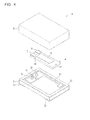
FIG. 4 is an exploded perspective view of a piezoelectric vibrator of an embodiment of the present invention. -
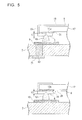
FIG. 5 is a partially enlarged view of a bonded portion of the piezoelectric vibrating piece and the bumps in an embodiment of the present invention. -
FIG. 6 is a flow chart representing a flow of the manufacture of a piezoelectric vibrator of an embodiment of the present invention. -
FIG. 7 is an explanatory diagram of one of the manufacturing steps of forming a piezoelectric vibrator along the flow chart ofFIG. 6 , showing changes in the surface shape of a crystal plate during the light etching of the crystal plate. -
FIG. 8 is an illustration of one of the manufacturing steps of forming a piezoelectric vibrator along the flow chart ofFIG. 6 , showing a state in which a plurality of depressions is formed in a lid substrate wafer formed into a lid substrate. -
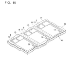
FIG. 9 is an illustration of one of the manufacturing steps of forming a piezoelectric vibrator along the flow chart ofFIG. 6 , showing a state in which a bonding film and inner electrodes are patterned on the upper surface of a base substrate wafer. -
FIG. 10 is a partially enlarged view (perspective view) ofFIG. 9 . -
FIG. 11 is an exploded perspective view of one of the manufacturing steps of forming a piezoelectric vibrator along the flow chart ofFIG. 6 , showing a wafer unit formed by the anodic bonding of a base substrate wafer and a lid substrate wafer with the piezoelectric vibrating piece housed in the cavity. -
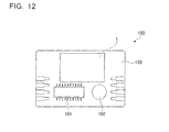
FIG. 12 is a schematic diagram illustrating an oscillator of an embodiment of the present invention. - An embodiment of the present invention is described below with reference to
FIG. 1 to FIG. 12 . - As illustrated in
FIG. 1 to FIG. 4 , a piezoelectric vibrator 1 is a surface-mounted piezoelectric vibrator including abase substrate 2 and alid substrate 3 stacked together in two layers in the form of a box, and apiezoelectric vibrating piece 4 housed in acavity 16 formed inside the vibrator. - In
FIG. 4 , throughelectrodes holes - The
piezoelectric vibrating piece 4 is an AT-cut vibrating piece formed from a crystal of piezoelectric material, and vibrates in response to an applied predetermined voltage. - The
piezoelectric vibrating piece 4 includes acrystal plate 17 substantially rectangular in shape in a planar view and having a uniform thickness, a pair ofexcitation electrodes crystal plate 17,extraction electrodes excitation electrodes mount electrodes extraction electrodes mount electrode 7 is electrically connected to aside electrode 15 of thecrystal plate 17 so as to be electrically connected to themount electrode 7 formed on the side of thecrystal plate 17 where theexcitation electrode 6 is provided. - The
excitation electrodes extraction electrodes mount electrodes side electrode 15 are formed of, for example, a gold (Au) coating. These films may be formed as conductive film coatings of, for example, chromium (Cr), nickel (Ni), aluminum (Al), or titanium (Ti), or as laminated films of such conductive films. - The piezoelectric
vibrating piece 4 structured as above is bump bonded on an upper surface of thebase substrate 2 usingbumps piece 4 is bump bonded with themount electrodes bumps inner electrodes 9 and 10 (described later) patterned on the upper surface of thebase substrate 2. In this way, the piezoelectricvibrating piece 4 is supported by being suspended above thebase substrate 2 with the distance corresponding to the thickness of thebumps mount electrodes inner electrodes - The
bumps mount electrodes - As illustrated in
FIG. 5 , anunderlying film 31 made of chromium is formed in regions of thecrystal plate 17 where themount electrodes mount electrodes underlying film 31. Themount electrodes extraction electrodes excitation electrodes side electrode 15. - At the point of bonding between the
mount electrodes bumps piece 4 is mounted and fixed in such a manner thattips bumps mount electrodes tips bumps underlying film 31. - Referring back to
FIG. 1 to FIG. 4 , thelid substrate 3 is a substrate made of a glass material, for example, soda-lime glass. On the side of the surface bonded to thebase substrate 2 is provided a rectangular depression (cavity) 16 where the piezoelectric vibratingpiece 4 is housed. Thedepression 16 is formed to provide a cavity when thebase substrate 2 and thelid substrate 3 are mated, thus providing thecavity 16 for housing the piezoelectric vibratingpiece 4. Thelid substrate 3 is anodically bonded to thebase substrate 2 with thedepression 16 facing thebase substrate 2. - The
base substrate 2 is a substrate made of a glass material, for example, soda-lime glass. Thebase substrate 2 is substantially planar in shape, and sized to be mated with thelid substrate 3. - The
base substrate 2 includes a pair of throughholes base substrate 2. One end of the throughholes cavity 16. Specifically, the one throughhole 24 is provided on the side of themount electrodes piece 4 mounted in position, and the other throughhole 25 is provided on the opposite side from themount electrodes piece 4. Further, the throughholes base substrate 2 substantially cylindrically, parallel to the thickness direction of thebase substrate 2. The through holes 24 and 25 may be tapered to gradually increase or decrease their diameters towards the lower surface of thebase substrate 2, for example. - In the through
holes electrodes holes electrodes holes cavity 16 air-tight, and to provide conduction betweenexternal electrodes 21 and 22 (described later) and theinner electrodes holes electrodes base substrate 2. - The upper surface side of the base substrate 2 (the side bonded to the lid substrate 3) is patterned with a
bonding film 23 for anodic bonding, and theinner electrodes bonding film 23 is formed along the periphery of thebase substrate 2, surrounding thedepression 16 formed in thelid substrate 3. - The
inner electrodes electrode 13 and the onemount electrode 7 of the piezoelectric vibratingpiece 4, and between the other throughelectrode 14 and theother mount electrode 8 of the piezoelectric vibratingpiece 4. Specifically, the oneinner electrode 9 is formed directly above the one throughelectrode 13 on the side of themount electrodes piece 4. The other inner electrode, theinner electrode 10, is formed directly above the other throughelectrode 14 by being routed along the piezoelectric vibratingpiece 4 from the position adjacent to the oneinner electrode 9 to the side opposite from the throughelectrode 13 appearing on thebase substrate 2. - The
bumps inner electrodes piece 4 is mounted using thebumps mount electrode 7 of the piezoelectric vibratingpiece 4 and one the throughelectrode 13 via the oneinner electrode 9, and between theother mount electrode 8 and the other throughelectrode 14 via the otherinner electrode 10. - On the lower surface of the
base substrate 2 are providedexternal electrodes electrodes external electrode 21, is electrically connected to the first excitation electrode, 5, of the piezoelectric vibratingpiece 4 via the one throughelectrode 13 and the oneinner electrode 9. The other external electrode, theexternal electrode 22, is electrically connected to the second excitation electrode, 6, of the piezoelectric vibratingpiece 4 via the other throughelectrode 14 and the otherinner electrode 10. - The piezoelectric vibrator 1 structured as above is activated by applying a predetermined drive voltage to the
external electrodes base substrate 2. In response, current flows through the first andsecond excitation electrodes piece 4, causing vibration at a predetermined frequency. The vibration can then be used as the timing source of control signals, or the reference signal source. - The following describes a method for manufacturing a plurality of piezoelectric vibrators 1 at once using a
base substrate wafer 40 and alid substrate wafer 50, with reference to the flow chart ofFIG. 6 . - First, the piezoelectric vibrating
piece 4 illustrated inFIG. 2 to FIG. 4 is fabricated in a piezoelectric vibrating piece fabrication step (S10). Specifically, a crystal of a lumbered quartz bar is sliced at a predetermined angle to provide a wafer of a constant thickness. The wafer is then coarsely processed by lapping, and mirror finished such as by polishing to obtain a constant thickness. After appropriately processing the wafer by treatment such as washing (S11), thecrystal plate 17 is lightly etched (S12). As illustrated inFIG. 7 , the light etching is performed by immersing thecrystal plate 17 in, for example, a hydrofluoric acid solution to planarize the surface of thecrystal plate 17. Then, theunderlying film 31 made of chromium is formed in regions of thecrystal plate 17 where themount electrodes underlying film 31 is formed in a thickness of, for example, 0.02 to 0.04 µm. Thereafter, a gold film is deposited and patterned on thecrystal plate 17 by photolithography to form theexcitation electrodes extraction electrodes mount electrodes excitation electrodes extraction electrodes mount electrodes side electrode 15 are formed in a thickness of, for example, 0.1 µm. Then, a gold film is overlaid in regions where themount electrodes mount electrodes pieces 4. - In addition, before, after or concurrently with this step, a first wafer fabrication step is performed in which the
lid substrate wafer 50 to be thelid substrate 3 is fabricated to make it usable for anodic bonding (S20). First, thelid substrate wafer 50, made of soda-lime glass, is polished to a predetermined thickness, and after washing, a disk-shapedlid substrate wafer 50 is formed from which the work-affected layer on the outermost surface has been removed by etching or the like, as illustrated inFIG. 8 (S21). This is followed by a depression forming step in which a plurality ofdepressions 16 to provide cavities is formed by methods such as etching and embossing in the row and column directions on the bonding face of the lid substrate wafer 50 (S22). After forming thedepressions 16, the surface having thedepressions 16 is polished in preparation for the bonding step (S60). This completes the first wafer fabrication step. - Concurrently with, or before or after this step (S20) or the piezoelectric vibration piece fabrication step (S10), a second wafer fabrication step is performed in which the
base substrate wafer 40 to be thebase substrate 2 is fabricated to make it usable for anodic bonding (S30). First, soda-lime glass is polished to a predetermined thickness, and after washing, a disk-shapedbase substrate wafer 40 is formed from which the work-affected layer on the outermost surface has been removed by etching or the like (S31). This is followed by a through electrodes forming step in which the pairs of throughelectrodes - Next, conductive material is patterned on the upper surface of the
base substrate wafer 40 to form the bonding film 23 (bonding film forming step; S33) and theinner electrodes electrodes FIGS. 9 and10 . Note that the dotted lines M shown inFIGS. 9 and10 are cutting lines used in the subsequent cutting step. - The through
electrodes base substrate wafer 40, as described above. Accordingly, theinner electrodes base substrate wafer 40 are closely in contact with the throughelectrodes inner electrode 9 and the one throughelectrode 13, and between the otherinner electrode 10 and the other throughelectrode 14. This completes the second wafer fabrication step. - In
FIG. 6 , the inner electrodes forming step (S34) is performed after the bonding film forming step (S33); however, the bonding film forming step (S33) may be performed after the inner electrodes forming step (S34), or these steps may be performed simultaneously. The same effect can be obtained regardless of the order of the steps. Accordingly, the order of these steps may be changed appropriately, as needed. - Then, the piezoelectric vibrating
pieces 4 fabricated as above are bonded to the upper surface of thebase substrate wafer 40 via their respectiveinner electrodes 9 and 10 (mount step; S40). First, thebumps inner electrodes - Then, with the basal portion of the piezoelectric vibrating
piece 4 placed on thebumps mount electrodes piece 4 are pressed against thebumps bumps bumps piece 4, and themount electrodes inner electrodes - Here, the piezoelectric vibrating
piece 4 is mounted and fixed in such a manner that thetips bumps mount electrodes piece 4 is mounted and fixed in such a manner that thetips bumps underlying film 31. Further, the bump bonding of themount electrode 7 of thecrystal plate 17 on thebump 11, and the bump bonding of themount electrode 8 of thecrystal plate 17 on thebump 12 supports thecrystal plate 17 substantially parallel to thebase substrate 2. As a result, the piezoelectric vibratingpiece 4 is supported by being suspended above thebase substrate wafer 40. Here, theexcitation electrodes piece 4 conduct to the throughelectrodes - After the piezoelectric vibrating
piece 4 is mounted, a mating step is performed in which thelid substrate wafer 50 is mated with the base substrate wafer 40 (S50). Specifically, thewafers piece 4 mounted as above is housed in thecavity 16 surrounded by thewafers - After the mating step, the mated two
wafers wafers bonding film 23 and thelid substrate wafer 50. This causes an electrochemical reaction at the interface between thebonding film 23 and thelid substrate wafer 50, anodically bonding the two with tight adhesion. - By the anodic bonding of the two
wafers piece 4 is sealed inside thecavity 16 maintained in a vacuum, and awafer unit 70 in which thebase substrate wafer 40 and thelid substrate wafer 50 are bonded together is obtained, as illustrated inFIG. 11 . Note that, inFIG. 11 , thewafer unit 70 is illustrated in an exploded view, and thebonding film 23 of thebase substrate wafer 40 is omitted for ease of illustration. The dotted lines M inFIG. 11 are cutting lines used in the subsequent cutting step. - At the time of anodic bonding, the through
holes base substrate wafer 40 are completely closed by the throughelectrodes cavity 16 will not be lost through the throughholes - After anodic bonding, an external electrodes forming step is performed in which conductive material is patterned on the lower surface of the
base substrate wafer 40 to form the pairs ofexternal electrodes electrodes external electrodes piece 4 sealed inside thecavity 16. - As in the case of the
inner electrodes electrodes base substrate wafer 40, theexternal electrodes electrodes external electrodes electrodes - Next, a cutting step is performed in which the
wafer unit 70 bonded as above is cut into individual pieces along the cutting lines M shown inFIG. 11 (S80). As a result, a plurality of bilayer, surface-mounted piezoelectric vibrators 1 illustrated inFIG. 1 is manufactured at once, each sealing the piezoelectric vibratingpiece 4 in thecavity 16 formed between the anodically bondedbase substrate 2 andlid substrate 3. - This is followed by an internal electrical characteristics test (S90). Specifically, measurement is made to check properties of the piezoelectric vibrating
piece 4, such as resonant frequency, resonant resistance, and drive level characteristics (excitation power dependence of resonant frequency and resonant resistance). Other properties, such as insulation resistance characteristics are also checked. Then, the piezoelectric vibrator 1 is subjected to an appearance test to check the dimensions, quality, and other conditions of the product. The manufacture of the piezoelectric vibrator 1 is finished upon completion of the checking. - In this embodiment, in the mount step, the piezoelectric vibrating
piece 4 is mounted and fixed in such a manner that thetips underlying film 31. This prevents the possible detachment from the bonding portion that may occur when thetips bumps crystal plate 17. More specifically, because the piezoelectric vibratingpiece 4 is mounted and fixed in such a manner that thetips bumps mount electrodes bumps mount electrodes piece 4 by flip-chip bonding. - Further, by the etching step performed before forming the
mount electrodes crystal plate 17, the surface irregularities of thecrystal plate 17 can be removed. This increases the bonding area for themount electrodes crystal plate 17, thereby improving the adhesion between thecrystal plate 17 and themount electrodes - Further, because the
underlying film 31 made of chromium is provided between thecrystal plate 17 and themount electrodes piece 4 is mounted and fixed in such a manner that thetips bumps mount electrodes underlying film 31 in the mount step, the adhesion between thecrystal plate 17 and themount electrodes bumps mount electrodes piece 4 by flip-chip bonding. - Further, because the
bumps mount electrodes bumps mount electrodes - When the
bumps mount electrodes tips bumps mount electrodes piece 4 detaches from thebumps piece 4 by flip-chip bonding. - An embodiment of an oscillator that uses a piezoelectric vibrator according to the present invention is described below with reference to
FIG. 12 . - As illustrated in
FIG. 12 , anoscillator 100 is structured to include the piezoelectric vibrator 1 provided as a resonator electrically connected to anintegrated circuit 101. Theoscillator 100 includes asubstrate 103 on whichelectronic components 102 such as capacitors are mounted. Theintegrated circuit 101 for the oscillator is mounted on thesubstrate 103, and the piezoelectric vibrator 1 is mounted in the vicinity of theintegrated circuit 101. Theelectronic components 102, theintegrated circuit 101, and the piezoelectric vibrator 1 are electrically connected to one another through wiring patterns (not shown). Note that each of these constituting elements is resin molded (not shown). - In the
oscillator 100 of this construction, applying a voltage to the piezoelectric vibrator 1 causes the piezoelectric vibratingpiece 4 in the piezoelectric vibrator 1 to vibrate. The vibration is transduced into an electrical signal by the piezoelectric characteristics of the piezoelectric vibratingpiece 4, and input to theintegrated circuit 101 as the electrical signal. The input electrical signal undergoes various processes in theintegrated circuit 101, and output as a frequency signal. In this way, the piezoelectric vibrator 1 serves as a resonator. - Further, by configuring the
integrated circuit 101 to be selectable according to requirements, for example, such as in an RTC (real-time clock) module, the oscillator can be provided not only as devices such as a single-function oscillator for clocks, but with additional functions, such as the control of operation date and time and the provision of a clock and a calendar, for these and external devices. - As described above, the
oscillator 100 of the present embodiment has high quality by virtue of using the piezoelectric vibrator 1 in which the mounting of the piezoelectric vibratingpiece 4 is ensured. Further, because the piezoelectric vibrator 1 can be produced with improved yield, the yield of theoscillator 100 is also improved. - It should be noted that the present invention is not limited to the embodiment described above, and various modifications of the embodiment that do not depart from the substance of the present invention are intended to be within the scope of the invention.
- For example, the piezoelectric vibrating piece exemplified as using an AT vibrating piece (thickness shear vibrating piece) in the foregoing embodiment may be adapted to use a tuning-fork piezoelectric or other vibrating piece.
- Further, the foregoing describes an embodiment in which the depressions are formed in the lid substrate; however, the depressions may be formed in the base substrate, or in the both substrates.
- Further, in the foregoing embodiment, the through electrodes are formed in the base substrate to enable voltage application from outside. However, instead of the through electrodes, electrodes may be formed that are routed to outside from the bonded portion of the base substrate and the lid substrate.
- Further, the foregoing describes an embodiment in which the underlying film is made of chromium; however, the underlying film may be made of conductive material such as aluminum and nickel. That is, materials that can improve the adhesion between the crystal plate and the electrodes made of metal material can be used. Further, the underlying film is not necessarily required, as long as the adhesion between the crystal plate and the electrodes is ensured. When the underlying film is not provided, the piezoelectric vibrating piece is mounted and fixed in such a manner that the tips of the bumps are not in contact with the crystal plate.
Claims (9)
- A method for manufacturing a piezoelectric vibrator (1) that comprises:a base substrate (2);a lid substrate (3) bonded to the base substrate with a cavity (16) between the base substrate and the lid substrate;a piezoelectric vibrating piece (4) housed in the cavity, the piezoelectric vibrating piece including a crystal plate (17) having on its outer surface excitation electrodes (5, 6) and mount electrodes (7, 8) electrically connected to the excitation electrodes;inner electrodes (9, 10) formed on the base substrate to be electrically connected to the piezoelectric vibrating piece; andmetal bumps (11, 12) formed on the inner electrodes to provide electrical interconnections between the inner electrodes and the mount electrodes, and to mount the piezoelectric vibrating piece in a cantilever fashion,the method comprising:forming the inner electrodes (9, 10) on the base substrate (2);forming the metal bumps (11, 12) on the inner electrodes; andbonding the mount electrodes (7, 8) of the piezoelectric vibrating piece (4) to the metal bumps, wherein the piezoelectric vibrating piece is mounted and fixed in such a manner that tips of the metal bumps are not in contact with the crystal plate (17).
- The method for manufacturing a piezoelectric vibrator according to claim 1, wherein the crystal plate is etched prior to forming the mount electrodes on the crystal plate.
- The method for manufacturing a piezoelectric vibrator according to claim 1 or claim 2,
wherein an underlying film (31) made of conductive material is formed in regions of the crystal plate where the mount electrodes are formed, and the mount electrodes are formed after forming the underlying film, and
wherein, upon bonding of the mount electrodes of the piezoelectric vibrating piece to the metal bumps, the piezoelectric vibrating piece is mounted and fixed in such a manner that the tips of the metal bumps are inside the mount electrodes and away from the interface between the mount electrodes and the underlying film. - The method for manufacturing a piezoelectric vibrator according to claim 3, wherein chromium is used for the underlying film.
- The method for manufacturing a piezoelectric vibrator according to any one of the preceding claims, wherein both the metal bumps and the mount electrodes are made of gold.
- A piezoelectric vibrator (1), comprising:a base substrate (2);a lid substrate (3) bonded to the base substrate with a cavity (16) between the base substrate and the lid substrate;a piezoelectric vibrating piece (4) housed in the cavity, the piezoelectric vibrating piece including a crystal plate (17) having on its outer surface excitation electrodes (5, 6) and mount electrodes (7, 8) electrically connected to the excitation electrodes;inner electrodes (9, 10) formed on the base substrate to be electrically connected to the piezoelectric vibrating piece; andmetal bumps (11, 2) formed on the inner electrodes to provide electrical interconnections between the inner electrodes and the mount electrodes, and to mount the piezoelectric vibrating piece in a cantilever fashion, wherein the metal bumps are mounted and fixed in such a manner that tips of the metal bumps are not in contact with the crystal plate.
- The piezoelectric vibrator according to claim 6, further comprising an underlying film (31) made of conductive material between the crystal plate and the mount electrodes.
- The piezoelectric vibrator according to claim 7, wherein the underlying film is formed of chromium.
- An oscillator (100), comprising:a piezoelectric vibrator according to any one of claims 6 to 8; andan integrated circuit (101) electrically connected to the piezoelectric vibrator provided as a resonator.
Applications Claiming Priority (1)
| Application Number | Priority Date | Filing Date | Title |
|---|---|---|---|
| JP2009031619A JP2010187326A (en) | 2009-02-13 | 2009-02-13 | Method for manufacturing piezoelectric vibrator, piezoelectric vibrator, and oscillator |
Publications (2)
| Publication Number | Publication Date |
|---|---|
| EP2219291A2 true EP2219291A2 (en) | 2010-08-18 |
| EP2219291A3 EP2219291A3 (en) | 2011-08-17 |
Family
ID=42169327
Family Applications (1)
| Application Number | Title | Priority Date | Filing Date |
|---|---|---|---|
| EP20100153369 Withdrawn EP2219291A3 (en) | 2009-02-13 | 2010-02-11 | Method for manufacturing piezoelectric vibrator, piezoelectric vibrator, and oscillator |
Country Status (6)
| Country | Link |
|---|---|
| US (1) | US8269568B2 (en) |
| EP (1) | EP2219291A3 (en) |
| JP (1) | JP2010187326A (en) |
| KR (1) | KR20100092916A (en) |
| CN (1) | CN101807896A (en) |
| TW (1) | TW201036222A (en) |
Families Citing this family (11)
| Publication number | Priority date | Publication date | Assignee | Title |
|---|---|---|---|---|
| JP5180975B2 (en) * | 2008-02-18 | 2013-04-10 | セイコーインスツル株式会社 | Piezoelectric vibrator manufacturing method and piezoelectric vibrator |
| WO2009122704A1 (en) * | 2008-03-31 | 2009-10-08 | 株式会社村田製作所 | Piezoelectric vibrating part |
| US8202786B2 (en) | 2010-07-15 | 2012-06-19 | Infineon Technologies Austria Ag | Method for manufacturing semiconductor devices having a glass substrate |
| US8865522B2 (en) | 2010-07-15 | 2014-10-21 | Infineon Technologies Austria Ag | Method for manufacturing semiconductor devices having a glass substrate |
| US9029200B2 (en) | 2010-07-15 | 2015-05-12 | Infineon Technologies Austria Ag | Method for manufacturing semiconductor devices having a metallisation layer |
| JP2012074837A (en) * | 2010-09-28 | 2012-04-12 | Nippon Dempa Kogyo Co Ltd | Piezoelectric device |
| JP5779030B2 (en) * | 2011-07-28 | 2015-09-16 | セイコーインスツル株式会社 | Electronic device, oscillator, and method of manufacturing electronic device |
| JP5827088B2 (en) * | 2011-09-27 | 2015-12-02 | セイコーインスツル株式会社 | Terminal connection structure of electronic parts, package, piezoelectric vibrator, oscillator, electronic equipment and radio clock |
| US10580605B2 (en) * | 2015-11-23 | 2020-03-03 | University Of Utah Research Foundation | Very low power microelectromechanical devices for the internet of everything |
| JP6845061B2 (en) * | 2017-03-24 | 2021-03-17 | 京セラ株式会社 | How to make a crystal device |
| CN113300689B (en) * | 2021-03-29 | 2023-01-31 | 天津大学 | Quartz resonator with reinforced structure, forming method thereof and electronic equipment |
Citations (7)
| Publication number | Priority date | Publication date | Assignee | Title |
|---|---|---|---|---|
| US1869160A (en) * | 1928-05-11 | 1932-07-26 | Bell Telephone Labor Inc | Piezo-electric resonator |
| JPH07109200A (en) * | 1993-10-08 | 1995-04-25 | Meidensha Corp | Crystal etching method |
| JPH07176971A (en) | 1992-07-03 | 1995-07-14 | Toyo Commun Equip Co Ltd | Structure of piezoelectric resonator |
| EP1127965A1 (en) * | 1999-05-18 | 2001-08-29 | Takaya Watanabe | Etching method and article processed by the method |
| US20040070462A1 (en) | 2002-10-10 | 2004-04-15 | Iyad Alhayek | Oscillator package |
| JP2005064582A (en) * | 2003-08-12 | 2005-03-10 | Stella Chemifa Corp | Quartz processing method, crystal plate obtained by the processing method, and etching composition for wet etching of quartz |
| JP2007096899A (en) | 2005-09-29 | 2007-04-12 | Seiko Epson Corp | Method for manufacturing piezoelectric vibrating piece, bonding structure of piezoelectric vibrating piece, piezoelectric device |
Family Cites Families (8)
| Publication number | Priority date | Publication date | Assignee | Title |
|---|---|---|---|---|
| US5925502A (en) | 1994-05-20 | 1999-07-20 | The United States Of America As Represented By The Secretary Of The Army | Method of metallizing a quartz resonator |
| JP2000124755A (en) | 1998-10-13 | 2000-04-28 | Hokuriku Electric Ind Co Ltd | Surface mount type crystal unit and method of manufacturing the same |
| JP2000341041A (en) * | 1999-05-26 | 2000-12-08 | Mitsumi Electric Co Ltd | Oscillator and manufacturing method thereof |
| JP2004254012A (en) * | 2003-02-19 | 2004-09-09 | Citizen Watch Co Ltd | Structure for supporting piezoelectric vibrator |
| JP2006101244A (en) * | 2004-09-29 | 2006-04-13 | Kyocera Kinseki Corp | Piezoelectric vibrator and manufacturing method thereof |
| DE602005012488D1 (en) * | 2005-06-09 | 2009-03-12 | Eta Sa Mft Horlogere Suisse | Compact piezoelectric resonator |
| US7888850B2 (en) * | 2007-01-30 | 2011-02-15 | Nihon Dempa Kogyo Co., Ltd. | Tuning-fork type piezoelectric unit |
| JP5100408B2 (en) * | 2007-01-30 | 2012-12-19 | 日本電波工業株式会社 | Tuning fork type piezoelectric vibrator |
-
2009
- 2009-02-13 JP JP2009031619A patent/JP2010187326A/en not_active Withdrawn
-
2010
- 2010-01-21 TW TW99101643A patent/TW201036222A/en unknown
- 2010-02-05 US US12/701,040 patent/US8269568B2/en not_active Expired - Fee Related
- 2010-02-11 CN CN201010115323A patent/CN101807896A/en active Pending
- 2010-02-11 EP EP20100153369 patent/EP2219291A3/en not_active Withdrawn
- 2010-02-12 KR KR20100013581A patent/KR20100092916A/en not_active Withdrawn
Patent Citations (7)
| Publication number | Priority date | Publication date | Assignee | Title |
|---|---|---|---|---|
| US1869160A (en) * | 1928-05-11 | 1932-07-26 | Bell Telephone Labor Inc | Piezo-electric resonator |
| JPH07176971A (en) | 1992-07-03 | 1995-07-14 | Toyo Commun Equip Co Ltd | Structure of piezoelectric resonator |
| JPH07109200A (en) * | 1993-10-08 | 1995-04-25 | Meidensha Corp | Crystal etching method |
| EP1127965A1 (en) * | 1999-05-18 | 2001-08-29 | Takaya Watanabe | Etching method and article processed by the method |
| US20040070462A1 (en) | 2002-10-10 | 2004-04-15 | Iyad Alhayek | Oscillator package |
| JP2005064582A (en) * | 2003-08-12 | 2005-03-10 | Stella Chemifa Corp | Quartz processing method, crystal plate obtained by the processing method, and etching composition for wet etching of quartz |
| JP2007096899A (en) | 2005-09-29 | 2007-04-12 | Seiko Epson Corp | Method for manufacturing piezoelectric vibrating piece, bonding structure of piezoelectric vibrating piece, piezoelectric device |
Also Published As
| Publication number | Publication date |
|---|---|
| EP2219291A3 (en) | 2011-08-17 |
| KR20100092916A (en) | 2010-08-23 |
| JP2010187326A (en) | 2010-08-26 |
| CN101807896A (en) | 2010-08-18 |
| US8269568B2 (en) | 2012-09-18 |
| TW201036222A (en) | 2010-10-01 |
| US20100207697A1 (en) | 2010-08-19 |
Similar Documents
| Publication | Publication Date | Title |
|---|---|---|
| US8269568B2 (en) | Method for manufacturing piezoelectric vibrator, piezoelectric vibrator, and oscillator | |
| US8702891B2 (en) | Method for manufacturing glass-sealed package, apparatus for manufacturing glass-sealed package, and oscillator | |
| US20100207696A1 (en) | Piezoelectric vibrator, method for manufacturing piezoelectric vibrator, and oscillator | |
| US8120234B2 (en) | Piezoelectric frames and piezoelectric devices comprising same | |
| US8875362B2 (en) | Method of manufacturing piezoelectric device | |
| KR101841767B1 (en) | Manufacturing method of electronic device package, electronic device package, and oscillator | |
| CN102254836B (en) | The manufacture method of electron device package part, electron device package part and oscillator | |
| CN103944532B (en) | The manufacturing method of electronic device and electronic device | |
| US8319404B2 (en) | Surface-mountable quartz-crystal devices and methods for manufacturing same | |
| US8664837B2 (en) | Piezoelectric device and method for fabricating the same | |
| JP5550373B2 (en) | Package manufacturing method | |
| JP2009165006A (en) | Piezoelectric vibrating piece, piezoelectric device, and tuning fork type piezoelectric vibrator frequency adjusting method | |
| US8499443B2 (en) | Method of manufacturing a piezoelectric vibrator | |
| US8341814B2 (en) | Methods for manufacturing piezoelectric devices | |
| US20130278114A1 (en) | Piezoelectric device and method for fabricating the same | |
| US8624470B2 (en) | Piezoelectric devices including electrode-less vibrating portions | |
| JP2007096945A (en) | Quartz vibrating device and method for manufacturing quartz vibrating device | |
| JP2010187268A (en) | Glass package, piezoelectric vibrator, method for marking glass package, and oscillator | |
| WO2021095294A1 (en) | Piezoelectric vibrator and method for manufacturing same | |
| JP2010273350A (en) | Method for adjusting frequency of piezoelectric device | |
| JP2011193291A (en) | Package, and method of manufacturing package | |
| JP2011091668A (en) | Piezoelectric oscillator and method for manufacturing the same |
Legal Events
| Date | Code | Title | Description |
|---|---|---|---|
| PUAI | Public reference made under article 153(3) epc to a published international application that has entered the european phase |
Free format text: ORIGINAL CODE: 0009012 |
|
| AK | Designated contracting states |
Kind code of ref document: A2 Designated state(s): AT BE BG CH CY CZ DE DK EE ES FI FR GB GR HR HU IE IS IT LI LT LU LV MC MK MT NL NO PL PT RO SE SI SK SM TR |
|
| AX | Request for extension of the european patent |
Extension state: AL BA RS |
|
| PUAL | Search report despatched |
Free format text: ORIGINAL CODE: 0009013 |
|
| RIC1 | Information provided on ipc code assigned before grant |
Ipc: H03H 9/02 20060101ALI20110707BHEP Ipc: H03H 9/05 20060101ALI20110707BHEP Ipc: H03H 9/10 20060101ALI20110707BHEP Ipc: H03H 3/02 20060101AFI20110707BHEP |
|
| AK | Designated contracting states |
Kind code of ref document: A3 Designated state(s): AT BE BG CH CY CZ DE DK EE ES FI FR GB GR HR HU IE IS IT LI LT LU LV MC MK MT NL NO PL PT RO SE SI SK SM TR |
|
| AX | Request for extension of the european patent |
Extension state: AL BA RS |
|
| 17P | Request for examination filed |
Effective date: 20120217 |
|
| 17Q | First examination report despatched |
Effective date: 20130319 |
|
| STAA | Information on the status of an ep patent application or granted ep patent |
Free format text: STATUS: THE APPLICATION IS DEEMED TO BE WITHDRAWN |
|
| 18D | Application deemed to be withdrawn |
Effective date: 20130730 |