EP2219234A2 - Method of manufacturing semiconductor light emitting device - Google Patents
Method of manufacturing semiconductor light emitting device Download PDFInfo
- Publication number
- EP2219234A2 EP2219234A2 EP20100153873 EP10153873A EP2219234A2 EP 2219234 A2 EP2219234 A2 EP 2219234A2 EP 20100153873 EP20100153873 EP 20100153873 EP 10153873 A EP10153873 A EP 10153873A EP 2219234 A2 EP2219234 A2 EP 2219234A2
- Authority
- EP
- European Patent Office
- Prior art keywords
- layer
- light emitting
- conductive
- semiconductor layer
- support member
- Prior art date
- Legal status (The legal status is an assumption and is not a legal conclusion. Google has not performed a legal analysis and makes no representation as to the accuracy of the status listed.)
- Granted
Links
Images


Classifications
-
- H—ELECTRICITY
- H10—SEMICONDUCTOR DEVICES; ELECTRIC SOLID-STATE DEVICES NOT OTHERWISE PROVIDED FOR
- H10H—INORGANIC LIGHT-EMITTING SEMICONDUCTOR DEVICES HAVING POTENTIAL BARRIERS
- H10H20/00—Individual inorganic light-emitting semiconductor devices having potential barriers, e.g. light-emitting diodes [LED]
- H10H20/01—Manufacture or treatment
- H10H20/011—Manufacture or treatment of bodies, e.g. forming semiconductor layers
- H10H20/018—Bonding of wafers
-
- H—ELECTRICITY
- H10—SEMICONDUCTOR DEVICES; ELECTRIC SOLID-STATE DEVICES NOT OTHERWISE PROVIDED FOR
- H10H—INORGANIC LIGHT-EMITTING SEMICONDUCTOR DEVICES HAVING POTENTIAL BARRIERS
- H10H20/00—Individual inorganic light-emitting semiconductor devices having potential barriers, e.g. light-emitting diodes [LED]
- H10H20/80—Constructional details
- H10H20/85—Packages
- H10H20/857—Interconnections, e.g. lead-frames, bond wires or solder balls
Definitions
- the embodiment relates to a method of manufacturing a semiconductor light emitting device.
- Groups III-V nitride semiconductors have been extensively used as main materials for light emitting devices, such as a light emitting diode (LED) or a laser diode (LD), due to the physical and chemical characteristics thereof.
- the groups III-V nitride semiconductors include a semiconductor material having a compositional formula of In x Al y Ga 1-x-y N (0 ⁇ x ⁇ 1, 0 ⁇ y ⁇ 1, and 0 ⁇ x+y ⁇ 1).
- the LED is a semiconductor device, which transmits/receives signals by converting an electric signal into infrared ray or light using the characteristics of compound semiconductors.
- the LED is also used as a light source.
- the LED or LD using the nitride semiconductor material is mainly used for the light emitting device to provide the light.
- the LED or the LD is used as a light source for various products, such as a keypad light emitting part of a cellular phone, an electric signboard, and an illumination device.
- the embodiment provides a method of manufacturing a semiconductor light emitting device capable of improving electrical characteristics.
- a method of manufacturing a semiconductor light emitting device includes forming a light emitting structure including a first conductive semiconductor layer, an active layer, and a second conductive semiconductor layer on a substrate, forming an electrode layer on the light emitting structure, forming a conductive support member on the electrode layer, and planarizing a top surface of the conductive support member.
- a method of manufacturing a semiconductor light emitting device includes forming a light emitting structure including a first conductive semiconductor layer, an active layer, and a second conductive semiconductor layer on a substrate, forming a channel layer on an outer peripheral portion of the light emitting structure, forming an electrode layer on the light emitting structure and the channel layer, forming a conductive support member on the electrode layer, and planarizing a top surface of the conductive support member.
- the embodiment can improve the electrical characteristics of the semiconductor light emitting device.
- each layer shown in the drawings can be exaggerated, omitted or schematically drawn for the purpose of convenience or clarity.
- the size of elements does not utterly reflect an actual size.
- FIG. 1 is a sectional view showing a semiconductor light emitting device 100 according to the embodiment.
- the semiconductor light emitting device 100 includes a first conductive semiconductor layer 110, an active layer 120, a second conductive semiconductor layer 130, a channel layer 140, an electrode layer 150, a conductive support member 170, and a first electrode 115.
- the first conductive semiconductor layer 110 may include an N-type semiconductor layer doped with first conductive dopants.
- the first conductive semiconductor layer 110 may include one of compound semiconductors such as GaN, InN, AlN, InGaN, AlGaN, InAlGaN, and AllnN.
- the first conductive dopant may be an N-type dopant selected from among Si, Ge, Sn, Se, and Te.
- the first electrode 115 having a predetermined pattern may be disposed below the first conductive semiconductor layer 110.
- the active layer 120 may be disposed on the first conductive semiconductor layer 110.
- the active layer 120 may have a single quantum well (SQW) structure or a multiple quantum well (MQW) structure.
- the active layer 120 may be formed in the SQW structure or the MQW structure at a one cycle of an InGaN well layer/GaN barrier layer.
- the material of a quantum well layer or a quantum barrier layer may be varied depending on a wavelength band of emitted light, but the embodiment is not limited thereto.
- a clad layer may be formed on and/or below the active layer 120.
- the second conductive semiconductor layer 130 may be formed on the active layer 120.
- the second conductive semiconductor layer 130 may include a P-type semiconductor layer doped with second conductive dopants.
- the second conductive semiconductor layer 130 may include one of compound semiconductors such as GaN, InN, AlN, InGaN, AlGaN, InAlGaN, and AllnN.
- the second conductive dopant includes a P-type dopant selected from among Mg, Be, and Zn.
- the first conductive semiconductor layer 110, the active layer 120, and the second conductive semiconductor layer 130 may be defined as a light emitting structure.
- the first conductive semiconductor layer 110 may include a P-type semiconductor layer
- the second conductive semiconductor layer 130 may include an N-type semiconductor layer.
- the light emitting structure may not only include an N-P junction structure, but include at least one of a P-N junction structure, an N-P-N junction structure, and a P-N-P junction structure.
- the channel layer 140 may be disposed below the second conductive semiconductor layer 130.
- the channel layer 140 may be disposed in the form of a frame on an outer peripheral portion of the second conductive semiconductor layer 130.
- the channel layer 140 may include an insulating material or a conductive material.
- the channel layer 140 may include a light transmissive layer.
- the channel layer 140 may be formed of at least one material selected from among SiO 2 , SiO x , SiO x N y , Si 3 N 4 , AI 2 O 3 , TiO 2 , ITO, IZO, AZO, IZTO, IAZO, IGZO, IGTO, and ATO. According to the embodiment, the channel layer 140 may not be formed.
- the channel layer 140 Since the channel layer 140 is exposed through an isolation etching process in the following mesa etching, the channel layer 140 may be designated as an isolation layer. In addition, since the channel layer 140 serves as an etching stopper in the isolation etching process, the channel layer 140 may be designated as an etching stop layer.
- the electrode layer 150 is disposed on the second conductive semiconductor layer 130.
- the electrode layer 150 may include at least one selected from Al, Ag, Pd, Rh, and Pt or the alloy thereof.
- the electrode layer 150 may include a reflective electrode material having an ohmic characteristic. A material having an ohmic characteristic may be disposed in a predetermined pattern between the electrode layer 150 and the second conductive semiconductor layer 130, but the embodiment is not limited thereto.
- the conductive support member 170 may be disposed on the electrode layer 150.
- the conductive support member 170 may include a material such as Cu, Au, Ni, or Mo.
- a surface (i.e., top surface) of the conductive support member 170 is planarized.
- the conductive support member 170 is bonded to a lead electrode by using a conductive adhesive after the conductive support member 170 has been positioned on a base, the conductive support member 170 can closely adhere to the lead electrode due to the planarized surface, so that electrical reliability can be improved.
- FIGS. 2 to 7 are sectional views showing the manufacturing process of the semiconductor light emitting device according to the embodiment.
- the first conductive semiconductor layer 110 is formed on a substrate 101.
- the active layer 120 is formed on the first conductive semiconductor layer 110.
- the second conductive semiconductor layer 130 is formed on the active layer 120.
- the substrate 101 may include one selected from the group consisting of Al 2 O 3 , GaN, SiC, ZnO, Si, GaP, InP, and GaAs.
- the substrate 101 is formed thereon with a buffer layer and/or undoped semiconductor layer.
- the buffer layer and/or undoped semiconductor layer may be removed in the manufacturing process of the semiconductor light emitting device thereafter.
- a nitride semiconductor may be grown on the substrate 101.
- the nitride semiconductor may be grown by an electronic beam depositor, physical vapor deposition (PVD), chemical vapor deposition (CVD), plasma laser deposition (PLD), a dual-type thermal evaporator, sputtering, or metal organic chemical vapor deposition (MOCVD), but the embodiment is not limited thereto.
- the first conductive semiconductor layer 110 may include an N-type semiconductor layer, and the second conductive semiconductor layer 130 may include a P-type semiconductor layer.
- the first conductive semiconductor layer 110 may include one of compound semiconductor materials such as GaN, InN, AIN, InGaN, AIGaN, InAlGaN, and AlInN.
- the first conductive semiconductor layer 110 may be doped with an N-type dopant (e.g., Si, Ge, Sn, Se, or Te).
- the second conductive semiconductor layer 130 may be doped with a P-type dopant such as Mg or Zn.
- the second conductive semiconductor layer 130 may include one of compound semiconductor materials such as GaN, InN, AlN, InGaN, AlGaN, InAlGaN, and AlInN.
- the first conductive semiconductor layer 110, the active layer 120, and the second conductive semiconductor layer 130 may be defined as the light emitting structure 135. Another semiconductor layer may be formed above and/or below the light emitting structure 135, but the embodiment is not limited thereto.
- the light emitting structure 135 may include at least one of an N-P junction structure, a P-N junction structure, an N-P-N junction structure, and a P-N-P junction structure.
- the channel layer 140 is formed on the second conductive semiconductor layer 130.
- the channel layer 140 is formed in the form of a frame on an outer peripheral portion of the second conductive semiconductor layer 130 such that an inner region 142 above the second conductive semiconductor layer 130 is open.
- the channel layer 140 may include at least one of SiO 2 , SiO x , SiO x N y , Si 3 N 4 , Al 2 O 3 , TiO 2 , ITO, IZO, AZO, IZTO, IAZO, IGZO, IGTO, and ATO.
- the channel layer 140 may be formed in the form of a polygonal frame or a circular frame on the second conductive semiconductor layer 130. The channel layer 140 improves adhesive strength with the second conductive semiconductor layer 130 to minimize delamination.
- the channel layer 140 may include a light transmissive conductive material or a light transmissive insulating material. If the channel layer 140 includes an insulating material, the gap between the second conductive semiconductor layer 130 and the conductive support member 170 can be widened by the channel layer 140.
- the electrode layer 150 may be formed on the second conductive semiconductor layer 130.
- the electrode layer 150 may include at least one of seed metal, ohmic metal, and reflective metal.
- the electrode layer 150 may include at least one selected from among Al, Ag, Pd, Rh, and Pt or the alloy thereof, but the embodiment is not limited thereto.
- the electrode layer 150 may be formed on the second conductive semiconductor layer 130 and the channel layer 140.
- the conductive support member 170 is formed on the electrode layer 150.
- the conductive support member 170 may be formed through an electroplating process.
- the conductive support member 170 may include Cu, Au, Ni, or Mo.
- a roughness section 175 is formed on a top surface of the conductive support member 170 after the electroplating process has been performed.
- the conductive support member 170 having a thickness of T1 is planarized by cutting or polishing the conductive support member 170 by a predetermined thickness of T2 (T2 ⁇ T1), such that the roughness section 175 can be removed.
- the roughness section 175 is formed, the following problems may occur. For example, when placing the conductive support member 170 on a base, stress may be transferred to a compound semiconductor due to the uneven roughness section 175 in a laser lift off (LLO) process. In this case, the wafer may be bent.
- LLO laser lift off
- the roughness section 175 is formed on the conductive support member 170, problems may occur in a probe process, a laser scribing process, a breaking process, or a sorting process. Particularly, in the probe process, an exact measurement result cannot be obtained due to the roughness section 175 formed on the conductive support member 170. In this case, the chip reliability may be degraded.
- the substrate 101 may be removed through a physical and/or chemical removing scheme.
- the substrate 101 may be removed through the LLO process.
- a laser beam having a predetermined wavelength band is irradiated onto the substrate 101 to remove the substrate 101.
- the buffer layer may be removed by using wet etchant to remove the substrate 101.
- the surface of the first conductive semiconductor layer 110 may be polished through an inductively coupled plasma/reactive ion etching (ICP/RIE) scheme.
- ICP/RIE inductively coupled plasma/reactive ion etching
- a mesa etching is performed with respect to the boundary region between chips (i.e., channel region) to remove the boundary region, thereby providing individual chips.
- the outer portion of the channel layer 140 is exposed by a groove 137 outside the light emitting structure 135.
- the first electrode 115 having a predetermined pattern is formed below the first conductive semiconductor layer 110.
- the first electrode 115 may be formed after or before the mesa etching is performed or after a chip dicing process is formed.
- the embodiment is applicable in the light emitting device for supplying light.
Landscapes
- Led Devices (AREA)
Abstract
Description
- The embodiment relates to a method of manufacturing a semiconductor light emitting device.
- Groups III-V nitride semiconductors have been extensively used as main materials for light emitting devices, such as a light emitting diode (LED) or a laser diode (LD), due to the physical and chemical characteristics thereof. For example, the groups III-V nitride semiconductors include a semiconductor material having a compositional formula of InxAlyGa1-x-yN (0≤x≤1, 0 ≤y≤1, and 0≤x+y≤1).
- The LED is a semiconductor device, which transmits/receives signals by converting an electric signal into infrared ray or light using the characteristics of compound semiconductors. The LED is also used as a light source.
- The LED or LD using the nitride semiconductor material is mainly used for the light emitting device to provide the light. For instance, the LED or the LD is used as a light source for various products, such as a keypad light emitting part of a cellular phone, an electric signboard, and an illumination device.
- The embodiment provides a method of manufacturing a semiconductor light emitting device capable of improving electrical characteristics.
- According to the embodiment, a method of manufacturing a semiconductor light emitting device includes forming a light emitting structure including a first conductive semiconductor layer, an active layer, and a second conductive semiconductor layer on a substrate, forming an electrode layer on the light emitting structure, forming a conductive support member on the electrode layer, and planarizing a top surface of the conductive support member.
- According to the embodiment, a method of manufacturing a semiconductor light emitting device includes forming a light emitting structure including a first conductive semiconductor layer, an active layer, and a second conductive semiconductor layer on a substrate, forming a channel layer on an outer peripheral portion of the light emitting structure, forming an electrode layer on the light emitting structure and the channel layer, forming a conductive support member on the electrode layer, and planarizing a top surface of the conductive support member.
- The embodiment can improve the electrical characteristics of the semiconductor light emitting device.
-
FIG. 1 is a sectional view showing a semiconductor light emitting device according to the embodiment; and -
FIGS. 2 to 7 are sectional views showing the manufacturing process of a semiconductor light emitting device according to the embodiment. - In the description of the embodiments, it will be understood that, when a layer (or film), a region, a pattern, or a structure is referred to as being "on" or "under" another substrate, another layer (or film), another region, another pad, or another pattern, it can be "directly" or "indirectly" on the other substrate, layer (or film), region, pad, or pattern, or one or more intervening layers may also be present. Such a position of the layer has been described with reference to the drawings.
- The thickness and size of each layer shown in the drawings can be exaggerated, omitted or schematically drawn for the purpose of convenience or clarity. In addition, the size of elements does not utterly reflect an actual size.
- Hereinafter, the embodiment will be described with reference to accompanying drawings.
-
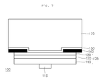
FIG. 1 is a sectional view showing a semiconductorlight emitting device 100 according to the embodiment. - Referring to
FIG. 1 , the semiconductorlight emitting device 100 includes a firstconductive semiconductor layer 110, anactive layer 120, a secondconductive semiconductor layer 130, achannel layer 140, anelectrode layer 150, aconductive support member 170, and afirst electrode 115. - The first
conductive semiconductor layer 110 may include an N-type semiconductor layer doped with first conductive dopants. For example, the firstconductive semiconductor layer 110 may include one of compound semiconductors such as GaN, InN, AlN, InGaN, AlGaN, InAlGaN, and AllnN. The first conductive dopant may be an N-type dopant selected from among Si, Ge, Sn, Se, and Te. - The
first electrode 115 having a predetermined pattern may be disposed below the firstconductive semiconductor layer 110. - The
active layer 120 may be disposed on the firstconductive semiconductor layer 110. Theactive layer 120 may have a single quantum well (SQW) structure or a multiple quantum well (MQW) structure. For example, theactive layer 120 may be formed in the SQW structure or the MQW structure at a one cycle of an InGaN well layer/GaN barrier layer. In theactive layer 120, the material of a quantum well layer or a quantum barrier layer may be varied depending on a wavelength band of emitted light, but the embodiment is not limited thereto. A clad layer may be formed on and/or below theactive layer 120. - The second
conductive semiconductor layer 130 may be formed on theactive layer 120. The secondconductive semiconductor layer 130 may include a P-type semiconductor layer doped with second conductive dopants. The secondconductive semiconductor layer 130 may include one of compound semiconductors such as GaN, InN, AlN, InGaN, AlGaN, InAlGaN, and AllnN. The second conductive dopant includes a P-type dopant selected from among Mg, Be, and Zn. - The first
conductive semiconductor layer 110, theactive layer 120, and the secondconductive semiconductor layer 130 may be defined as a light emitting structure. The firstconductive semiconductor layer 110 may include a P-type semiconductor layer, and the secondconductive semiconductor layer 130 may include an N-type semiconductor layer. Accordingly, the light emitting structure may not only include an N-P junction structure, but include at least one of a P-N junction structure, an N-P-N junction structure, and a P-N-P junction structure. - The
channel layer 140 may be disposed below the secondconductive semiconductor layer 130. Thechannel layer 140 may be disposed in the form of a frame on an outer peripheral portion of the secondconductive semiconductor layer 130. Thechannel layer 140 may include an insulating material or a conductive material. Thechannel layer 140 may include a light transmissive layer. For example, thechannel layer 140 may be formed of at least one material selected from among SiO2, SiOx, SiOxNy, Si3N4, AI2O3, TiO2, ITO, IZO, AZO, IZTO, IAZO, IGZO, IGTO, and ATO. According to the embodiment, thechannel layer 140 may not be formed. - Since the
channel layer 140 is exposed through an isolation etching process in the following mesa etching, thechannel layer 140 may be designated as an isolation layer. In addition, since thechannel layer 140 serves as an etching stopper in the isolation etching process, thechannel layer 140 may be designated as an etching stop layer. - The
electrode layer 150 is disposed on the secondconductive semiconductor layer 130. Theelectrode layer 150 may include at least one selected from Al, Ag, Pd, Rh, and Pt or the alloy thereof. In addition, theelectrode layer 150 may include a reflective electrode material having an ohmic characteristic. A material having an ohmic characteristic may be disposed in a predetermined pattern between theelectrode layer 150 and the secondconductive semiconductor layer 130, but the embodiment is not limited thereto. - The
conductive support member 170 may be disposed on theelectrode layer 150. Theconductive support member 170 may include a material such as Cu, Au, Ni, or Mo. - A surface (i.e., top surface) of the
conductive support member 170 is planarized. When theconductive support member 170 is bonded to a lead electrode by using a conductive adhesive after theconductive support member 170 has been positioned on a base, theconductive support member 170 can closely adhere to the lead electrode due to the planarized surface, so that electrical reliability can be improved. -
FIGS. 2 to 7 are sectional views showing the manufacturing process of the semiconductor light emitting device according to the embodiment. - Referring to
FIG. 2 , the firstconductive semiconductor layer 110 is formed on asubstrate 101. Theactive layer 120 is formed on the firstconductive semiconductor layer 110. The secondconductive semiconductor layer 130 is formed on theactive layer 120. - The
substrate 101 may include one selected from the group consisting of Al2O3, GaN, SiC, ZnO, Si, GaP, InP, and GaAs. Thesubstrate 101 is formed thereon with a buffer layer and/or undoped semiconductor layer. The buffer layer and/or undoped semiconductor layer may be removed in the manufacturing process of the semiconductor light emitting device thereafter. - A nitride semiconductor may be grown on the
substrate 101. The nitride semiconductor may be grown by an electronic beam depositor, physical vapor deposition (PVD), chemical vapor deposition (CVD), plasma laser deposition (PLD), a dual-type thermal evaporator, sputtering, or metal organic chemical vapor deposition (MOCVD), but the embodiment is not limited thereto. - The first
conductive semiconductor layer 110 may include an N-type semiconductor layer, and the secondconductive semiconductor layer 130 may include a P-type semiconductor layer. The firstconductive semiconductor layer 110 may include one of compound semiconductor materials such as GaN, InN, AIN, InGaN, AIGaN, InAlGaN, and AlInN. The firstconductive semiconductor layer 110 may be doped with an N-type dopant (e.g., Si, Ge, Sn, Se, or Te). The secondconductive semiconductor layer 130 may be doped with a P-type dopant such as Mg or Zn. The secondconductive semiconductor layer 130 may include one of compound semiconductor materials such as GaN, InN, AlN, InGaN, AlGaN, InAlGaN, and AlInN. - The first
conductive semiconductor layer 110, theactive layer 120, and the secondconductive semiconductor layer 130 may be defined as thelight emitting structure 135. Another semiconductor layer may be formed above and/or below thelight emitting structure 135, but the embodiment is not limited thereto. Thelight emitting structure 135 may include at least one of an N-P junction structure, a P-N junction structure, an N-P-N junction structure, and a P-N-P junction structure. - The
channel layer 140 is formed on the secondconductive semiconductor layer 130. Thechannel layer 140 is formed in the form of a frame on an outer peripheral portion of the secondconductive semiconductor layer 130 such that aninner region 142 above the secondconductive semiconductor layer 130 is open. Thechannel layer 140 may include at least one of SiO2, SiOx, SiOxNy, Si3N4, Al2O3, TiO2, ITO, IZO, AZO, IZTO, IAZO, IGZO, IGTO, and ATO. Thechannel layer 140 may be formed in the form of a polygonal frame or a circular frame on the secondconductive semiconductor layer 130. Thechannel layer 140 improves adhesive strength with the secondconductive semiconductor layer 130 to minimize delamination. Thechannel layer 140 may include a light transmissive conductive material or a light transmissive insulating material. If thechannel layer 140 includes an insulating material, the gap between the secondconductive semiconductor layer 130 and theconductive support member 170 can be widened by thechannel layer 140. - Referring to
FIG. 3 , theelectrode layer 150 may be formed on the secondconductive semiconductor layer 130. Theelectrode layer 150 may include at least one of seed metal, ohmic metal, and reflective metal. Theelectrode layer 150 may include at least one selected from among Al, Ag, Pd, Rh, and Pt or the alloy thereof, but the embodiment is not limited thereto. Theelectrode layer 150 may be formed on the secondconductive semiconductor layer 130 and thechannel layer 140. - Referring to
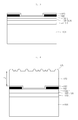
FIGS. 4 and5 , theconductive support member 170 is formed on theelectrode layer 150. Theconductive support member 170 may be formed through an electroplating process. Theconductive support member 170 may include Cu, Au, Ni, or Mo. - A
roughness section 175 is formed on a top surface of theconductive support member 170 after the electroplating process has been performed. - The
conductive support member 170 having a thickness of T1 is planarized by cutting or polishing theconductive support member 170 by a predetermined thickness of T2 (T2≤T1), such that theroughness section 175 can be removed. - If the
roughness section 175 is formed, the following problems may occur. For example, when placing theconductive support member 170 on a base, stress may be transferred to a compound semiconductor due to theuneven roughness section 175 in a laser lift off (LLO) process. In this case, the wafer may be bent. In addition, if theroughness section 175 is formed on theconductive support member 170, problems may occur in a probe process, a laser scribing process, a breaking process, or a sorting process. Particularly, in the probe process, an exact measurement result cannot be obtained due to theroughness section 175 formed on theconductive support member 170. In this case, the chip reliability may be degraded. - Referring to
FIGS. 5 and 6 , after theconductive support member 170 has been planarized, thesubstrate 101 may be removed through a physical and/or chemical removing scheme. For example, thesubstrate 101 may be removed through the LLO process. In other words, a laser beam having a predetermined wavelength band is irradiated onto thesubstrate 101 to remove thesubstrate 101. In addition, if another semiconductor layer (e.g., buffer layer) is formed between thesubstrate 101 and the firstconductive semiconductor layer 110, the buffer layer may be removed by using wet etchant to remove thesubstrate 101. After thesubstrate 101 has been removed, the surface of the firstconductive semiconductor layer 110 may be polished through an inductively coupled plasma/reactive ion etching (ICP/RIE) scheme. - As shown in
FIG. 6 , a mesa etching is performed with respect to the boundary region between chips (i.e., channel region) to remove the boundary region, thereby providing individual chips. In this case, the outer portion of thechannel layer 140 is exposed by agroove 137 outside thelight emitting structure 135. - Referring to
FIG. 7 , thefirst electrode 115 having a predetermined pattern is formed below the firstconductive semiconductor layer 110. Thefirst electrode 115 may be formed after or before the mesa etching is performed or after a chip dicing process is formed. - Although embodiments have been described with reference to a number of illustrative embodiments thereof, it should be understood that numerous other modifications and embodiments can be devised by those skilled in the art that will fall within this disclosure. More particularly, various variations and modifications are possible in the component parts and/or arrangements of the subject combination arrangement within the scope of the disclosure, the drawings and the appended claims. In addition to variations and modifications in the component parts and/or arrangements, alternative uses will also be apparent to those skilled in the art.
- The embodiment is applicable in the light emitting device for supplying light.
Claims (12)
- A method of manufacturing a semiconductor light emitting device (100), the method comprising:forming a light emitting structure including a first conductive semiconductor layer (110), an active layer (120), and a second conductive semiconductor layer (130) on a substrate;optionally forming a channel layer (140) on an outer peripheral portion of the light emitting structure;forming an electrode layer (150) on the light emitting structure and optionally on the channel layer;forming a conductive support member (170) on the electrode layer; andplanarizing a top surface of the conductive support member (170).
- The method of claim 1, further comprising:removing the substrate; andforming a first electrode (115) on the light emitting structure.
- The method of claim 1 or of claim 2, wherein the planarizing is performed by a polishing process.
- The method of any of preceding claims, wherein the material of the conductive support member (170) comprises at least a material chosen within the group consisting of Cu, Au, Ni, and Mo.
- The method of any of preceding claims, wherein the conductive support member (170) is formed through a plating process.
- The method of any of preceding claims, wherein the electrode layer (150) includes seed metal.
- The method of any of preceding claims, wherein the electrode layer (150) includes ohmic metal.
- The method of any of preceding claims, wherein the electrode layer (150) includes reflective metal.
- The method of any of preceding claims, wherein the material of the electrode layer (150) comprises at least a material chosen within the group consisting of Al, Ag, Pd, Rh, and Pt, or alloy thereof.
- The method of any of preceding claims which comprises forming a channel layer (140) and wherein the material of the channel layer comprises at least a material chosen within the group consisting of SiO2, SiOx, SiOxNy, Si3N4, Al2O3, TiO2, ITO, IZO, AZO, IZTO, IAZO, IGZO, IGTO, and ATO.
- The method of any of preceding claims which comprises forming a channel layer (140) and wherein the channel layer includes a light transmittive conductive material.
- The method of any of preceding claims which comprises forming a channel layer (140) and wherein the channel layer includes a light transmittive insulating material.
Applications Claiming Priority (1)
| Application Number | Priority Date | Filing Date | Title |
|---|---|---|---|
| KR1020090013171A KR100999793B1 (en) | 2009-02-17 | 2009-02-17 | Method of manufacturing semiconductor light emitting device |
Publications (3)
| Publication Number | Publication Date |
|---|---|
| EP2219234A2 true EP2219234A2 (en) | 2010-08-18 |
| EP2219234A3 EP2219234A3 (en) | 2010-11-24 |
| EP2219234B1 EP2219234B1 (en) | 2016-11-30 |
Family
ID=42144951
Family Applications (1)
| Application Number | Title | Priority Date | Filing Date |
|---|---|---|---|
| EP10153873.4A Active EP2219234B1 (en) | 2009-02-17 | 2010-02-17 | Method of manufacturing semiconductor light emitting device |
Country Status (4)
| Country | Link |
|---|---|
| US (2) | US8236581B2 (en) |
| EP (1) | EP2219234B1 (en) |
| KR (1) | KR100999793B1 (en) |
| CN (1) | CN101807655B (en) |
Families Citing this family (1)
| Publication number | Priority date | Publication date | Assignee | Title |
|---|---|---|---|---|
| CN102142517B (en) * | 2010-12-17 | 2017-02-08 | 华中科技大学 | Multiple-layer phase-change material with low thermal conductivity |
Family Cites Families (25)
| Publication number | Priority date | Publication date | Assignee | Title |
|---|---|---|---|---|
| JP2002353506A (en) * | 2001-05-23 | 2002-12-06 | Sharp Corp | Semiconductor light emitting device and method of manufacturing the same |
| JP2002368273A (en) * | 2001-06-07 | 2002-12-20 | Hitachi Cable Ltd | Semiconductor light emitting device |
| TW577178B (en) * | 2002-03-04 | 2004-02-21 | United Epitaxy Co Ltd | High efficient reflective metal layer of light emitting diode |
| US20040140474A1 (en) * | 2002-06-25 | 2004-07-22 | Matsushita Electric Industrial Co., Ltd. | Semiconductor light-emitting device, method for fabricating the same and method for bonding the same |
| US20060273324A1 (en) * | 2003-07-28 | 2006-12-07 | Makoto Asai | Light-emitting diode and process for producing the same |
| JP2005044954A (en) | 2003-07-28 | 2005-02-17 | Toyoda Gosei Co Ltd | Method for forming electrode on semiconductor substrate |
| TWI234298B (en) * | 2003-11-18 | 2005-06-11 | Itswell Co Ltd | Semiconductor light emitting diode and method for manufacturing the same |
| JP4616830B2 (en) * | 2004-04-28 | 2011-01-19 | 富士通株式会社 | Manufacturing method of semiconductor device |
| KR100661709B1 (en) | 2004-12-23 | 2006-12-26 | 엘지이노텍 주식회사 | Nitride semiconductor light emitting device and manufacturing method |
| US7432119B2 (en) * | 2005-01-11 | 2008-10-07 | Semileds Corporation | Light emitting diode with conducting metal substrate |
| KR100976268B1 (en) * | 2005-04-04 | 2010-08-18 | 가부시키가이샤 토호쿠 테크노 아치 | BAN single crystal growth method, BAN substrate fabrication method, BAN device manufacturing method and BAN device |
| KR100640978B1 (en) | 2005-06-07 | 2006-11-02 | 동부일렉트로닉스 주식회사 | Manufacturing Method of CMOS Image Sensor |
| SG130975A1 (en) * | 2005-09-29 | 2007-04-26 | Tinggi Tech Private Ltd | Fabrication of semiconductor devices for light emission |
| TW200735418A (en) * | 2005-11-22 | 2007-09-16 | Rohm Co Ltd | Nitride semiconductor device |
| JP5047516B2 (en) | 2006-03-23 | 2012-10-10 | 昭和電工株式会社 | Method for manufacturing gallium nitride compound semiconductor light emitting device, gallium nitride compound semiconductor light emitting device, and lamp using the same |
| JP4864766B2 (en) * | 2006-03-31 | 2012-02-01 | 富士フイルム株式会社 | Method for forming semiconductor layer |
| WO2007148866A1 (en) | 2006-06-23 | 2007-12-27 | Lg Electronics Inc. | Light emitting diode having vertical topology and method of making the same |
| JP2008053685A (en) * | 2006-08-23 | 2008-03-06 | Samsung Electro Mech Co Ltd | Vertical structure gallium nitride based light-emitting diode device and method of manufacturing the same |
| KR100826412B1 (en) | 2006-11-03 | 2008-04-29 | 삼성전기주식회사 | Nitride semiconductor light emitting device and manufacturing method |
| KR100872717B1 (en) * | 2007-06-22 | 2008-12-05 | 엘지이노텍 주식회사 | Light emitting device and manufacturing method |
| US20090004764A1 (en) | 2007-06-29 | 2009-01-01 | Semiconductor Energy Laboratory Co., Ltd. | Method for manufacturing SOI substrate and method for manufacturing semiconductor device |
| WO2009005477A1 (en) | 2007-07-04 | 2009-01-08 | Tinggi Technologies Private Limited | Separation of semiconductor devices |
| TWI350563B (en) * | 2007-07-10 | 2011-10-11 | Delta Electronics Inc | Manufacturing method of light emitting diode apparatus |
| KR101438811B1 (en) | 2008-01-03 | 2014-09-05 | 엘지이노텍 주식회사 | Semiconductor light emitting device and manufacturing method thereof |
| KR100992657B1 (en) | 2009-02-16 | 2010-11-05 | 엘지이노텍 주식회사 | Semiconductor light emitting device and manufacturing method thereof |
-
2009
- 2009-02-17 KR KR1020090013171A patent/KR100999793B1/en not_active Expired - Fee Related
-
2010
- 2010-02-16 US US12/706,335 patent/US8236581B2/en not_active Expired - Fee Related
- 2010-02-17 EP EP10153873.4A patent/EP2219234B1/en active Active
- 2010-02-20 CN CN2010101215182A patent/CN101807655B/en active Active
-
2012
- 2012-07-11 US US13/546,826 patent/US8785963B2/en active Active
Non-Patent Citations (1)
| Title |
|---|
| None |
Also Published As
| Publication number | Publication date |
|---|---|
| US8236581B2 (en) | 2012-08-07 |
| CN101807655B (en) | 2013-12-18 |
| US8785963B2 (en) | 2014-07-22 |
| US20100210058A1 (en) | 2010-08-19 |
| CN101807655A (en) | 2010-08-18 |
| EP2219234A3 (en) | 2010-11-24 |
| US20120273825A1 (en) | 2012-11-01 |
| KR100999793B1 (en) | 2010-12-08 |
| EP2219234B1 (en) | 2016-11-30 |
| KR20100093991A (en) | 2010-08-26 |
Similar Documents
| Publication | Publication Date | Title |
|---|---|---|
| JP6386015B2 (en) | Light emitting element | |
| EP2187456B1 (en) | Semiconductor light emitting device | |
| EP2228838B1 (en) | Light emtting device, method for manufacturing light emitting device, and light emitting apparatus | |
| KR100986560B1 (en) | Light emitting device and fabrication method thereof | |
| EP2187455A1 (en) | Semiconductor light emitting device | |
| US8901599B2 (en) | Semiconductor light emitting device | |
| EP2194585A1 (en) | Semiconductor light emitting device | |
| EP2317575B1 (en) | Semiconductor light emitting device and method for manufacturing same | |
| EP2219237A2 (en) | Semiconductor light emitting device and method of manufacturing the same | |
| EP2187458B1 (en) | Semiconductor light emitting device with shock protection | |
| EP2224502B1 (en) | Semiconductor light emitting device | |
| EP2219234B1 (en) | Method of manufacturing semiconductor light emitting device | |
| KR101199129B1 (en) | Semiconductor light emitting device and fabrication method thereof | |
| KR101500027B1 (en) | Semiconductor light emitting device |
Legal Events
| Date | Code | Title | Description |
|---|---|---|---|
| PUAI | Public reference made under article 153(3) epc to a published international application that has entered the european phase |
Free format text: ORIGINAL CODE: 0009012 |
|
| 17P | Request for examination filed |
Effective date: 20100217 |
|
| AK | Designated contracting states |
Kind code of ref document: A2 Designated state(s): AT BE BG CH CY CZ DE DK EE ES FI FR GB GR HR HU IE IS IT LI LT LU LV MC MK MT NL NO PL PT RO SE SI SK SM TR |
|
| AX | Request for extension of the european patent |
Extension state: AL BA RS |
|
| RAP1 | Party data changed (applicant data changed or rights of an application transferred) |
Owner name: LG INNOTEK CO., LTD. |
|
| PUAL | Search report despatched |
Free format text: ORIGINAL CODE: 0009013 |
|
| AK | Designated contracting states |
Kind code of ref document: A3 Designated state(s): AT BE BG CH CY CZ DE DK EE ES FI FR GB GR HR HU IE IS IT LI LT LU LV MC MK MT NL NO PL PT RO SE SI SK SM TR |
|
| AX | Request for extension of the european patent |
Extension state: AL BA RS |
|
| RAP1 | Party data changed (applicant data changed or rights of an application transferred) |
Owner name: LG INNOTEK CO., LTD. |
|
| 17Q | First examination report despatched |
Effective date: 20150504 |
|
| GRAP | Despatch of communication of intention to grant a patent |
Free format text: ORIGINAL CODE: EPIDOSNIGR1 |
|
| INTG | Intention to grant announced |
Effective date: 20160629 |
|
| RIN1 | Information on inventor provided before grant (corrected) |
Inventor name: JUNG, JOO YONG |
|
| GRAS | Grant fee paid |
Free format text: ORIGINAL CODE: EPIDOSNIGR3 |
|
| GRAA | (expected) grant |
Free format text: ORIGINAL CODE: 0009210 |
|
| AK | Designated contracting states |
Kind code of ref document: B1 Designated state(s): AT BE BG CH CY CZ DE DK EE ES FI FR GB GR HR HU IE IS IT LI LT LU LV MC MK MT NL NO PL PT RO SE SI SK SM TR |
|
| REG | Reference to a national code |
Ref country code: CH Ref legal event code: EP Ref country code: GB Ref legal event code: FG4D |
|
| REG | Reference to a national code |
Ref country code: AT Ref legal event code: REF Ref document number: 850545 Country of ref document: AT Kind code of ref document: T Effective date: 20161215 |
|
| REG | Reference to a national code |
Ref country code: IE Ref legal event code: FG4D |
|
| REG | Reference to a national code |
Ref country code: DE Ref legal event code: R096 Ref document number: 602010038370 Country of ref document: DE |
|
| REG | Reference to a national code |
Ref country code: FR Ref legal event code: PLFP Year of fee payment: 8 |
|
| PG25 | Lapsed in a contracting state [announced via postgrant information from national office to epo] |
Ref country code: LV Free format text: LAPSE BECAUSE OF FAILURE TO SUBMIT A TRANSLATION OF THE DESCRIPTION OR TO PAY THE FEE WITHIN THE PRESCRIBED TIME-LIMIT Effective date: 20161130 |
|
| REG | Reference to a national code |
Ref country code: NL Ref legal event code: FP |
|
| REG | Reference to a national code |
Ref country code: LT Ref legal event code: MG4D |
|
| REG | Reference to a national code |
Ref country code: AT Ref legal event code: MK05 Ref document number: 850545 Country of ref document: AT Kind code of ref document: T Effective date: 20161130 |
|
| PG25 | Lapsed in a contracting state [announced via postgrant information from national office to epo] |
Ref country code: NO Free format text: LAPSE BECAUSE OF FAILURE TO SUBMIT A TRANSLATION OF THE DESCRIPTION OR TO PAY THE FEE WITHIN THE PRESCRIBED TIME-LIMIT Effective date: 20170228 Ref country code: GR Free format text: LAPSE BECAUSE OF FAILURE TO SUBMIT A TRANSLATION OF THE DESCRIPTION OR TO PAY THE FEE WITHIN THE PRESCRIBED TIME-LIMIT Effective date: 20170301 Ref country code: LT Free format text: LAPSE BECAUSE OF FAILURE TO SUBMIT A TRANSLATION OF THE DESCRIPTION OR TO PAY THE FEE WITHIN THE PRESCRIBED TIME-LIMIT Effective date: 20161130 Ref country code: SE Free format text: LAPSE BECAUSE OF FAILURE TO SUBMIT A TRANSLATION OF THE DESCRIPTION OR TO PAY THE FEE WITHIN THE PRESCRIBED TIME-LIMIT Effective date: 20161130 |
|
| RAP2 | Party data changed (patent owner data changed or rights of a patent transferred) |
Owner name: LG INNOTEK CO., LTD. |
|
| PG25 | Lapsed in a contracting state [announced via postgrant information from national office to epo] |
Ref country code: ES Free format text: LAPSE BECAUSE OF FAILURE TO SUBMIT A TRANSLATION OF THE DESCRIPTION OR TO PAY THE FEE WITHIN THE PRESCRIBED TIME-LIMIT Effective date: 20161130 Ref country code: PT Free format text: LAPSE BECAUSE OF FAILURE TO SUBMIT A TRANSLATION OF THE DESCRIPTION OR TO PAY THE FEE WITHIN THE PRESCRIBED TIME-LIMIT Effective date: 20170330 Ref country code: FI Free format text: LAPSE BECAUSE OF FAILURE TO SUBMIT A TRANSLATION OF THE DESCRIPTION OR TO PAY THE FEE WITHIN THE PRESCRIBED TIME-LIMIT Effective date: 20161130 Ref country code: AT Free format text: LAPSE BECAUSE OF FAILURE TO SUBMIT A TRANSLATION OF THE DESCRIPTION OR TO PAY THE FEE WITHIN THE PRESCRIBED TIME-LIMIT Effective date: 20161130 Ref country code: BE Free format text: LAPSE BECAUSE OF NON-PAYMENT OF DUE FEES Effective date: 20170228 Ref country code: PL Free format text: LAPSE BECAUSE OF FAILURE TO SUBMIT A TRANSLATION OF THE DESCRIPTION OR TO PAY THE FEE WITHIN THE PRESCRIBED TIME-LIMIT Effective date: 20161130 Ref country code: HR Free format text: LAPSE BECAUSE OF FAILURE TO SUBMIT A TRANSLATION OF THE DESCRIPTION OR TO PAY THE FEE WITHIN THE PRESCRIBED TIME-LIMIT Effective date: 20161130 |
|
| PG25 | Lapsed in a contracting state [announced via postgrant information from national office to epo] |
Ref country code: EE Free format text: LAPSE BECAUSE OF FAILURE TO SUBMIT A TRANSLATION OF THE DESCRIPTION OR TO PAY THE FEE WITHIN THE PRESCRIBED TIME-LIMIT Effective date: 20161130 Ref country code: CZ Free format text: LAPSE BECAUSE OF FAILURE TO SUBMIT A TRANSLATION OF THE DESCRIPTION OR TO PAY THE FEE WITHIN THE PRESCRIBED TIME-LIMIT Effective date: 20161130 Ref country code: DK Free format text: LAPSE BECAUSE OF FAILURE TO SUBMIT A TRANSLATION OF THE DESCRIPTION OR TO PAY THE FEE WITHIN THE PRESCRIBED TIME-LIMIT Effective date: 20161130 Ref country code: RO Free format text: LAPSE BECAUSE OF FAILURE TO SUBMIT A TRANSLATION OF THE DESCRIPTION OR TO PAY THE FEE WITHIN THE PRESCRIBED TIME-LIMIT Effective date: 20161130 Ref country code: SK Free format text: LAPSE BECAUSE OF FAILURE TO SUBMIT A TRANSLATION OF THE DESCRIPTION OR TO PAY THE FEE WITHIN THE PRESCRIBED TIME-LIMIT Effective date: 20161130 |
|
| PG25 | Lapsed in a contracting state [announced via postgrant information from national office to epo] |
Ref country code: BG Free format text: LAPSE BECAUSE OF FAILURE TO SUBMIT A TRANSLATION OF THE DESCRIPTION OR TO PAY THE FEE WITHIN THE PRESCRIBED TIME-LIMIT Effective date: 20170228 Ref country code: IT Free format text: LAPSE BECAUSE OF FAILURE TO SUBMIT A TRANSLATION OF THE DESCRIPTION OR TO PAY THE FEE WITHIN THE PRESCRIBED TIME-LIMIT Effective date: 20161130 Ref country code: SM Free format text: LAPSE BECAUSE OF FAILURE TO SUBMIT A TRANSLATION OF THE DESCRIPTION OR TO PAY THE FEE WITHIN THE PRESCRIBED TIME-LIMIT Effective date: 20161130 Ref country code: BE Free format text: LAPSE BECAUSE OF FAILURE TO SUBMIT A TRANSLATION OF THE DESCRIPTION OR TO PAY THE FEE WITHIN THE PRESCRIBED TIME-LIMIT Effective date: 20161130 |
|
| REG | Reference to a national code |
Ref country code: DE Ref legal event code: R097 Ref document number: 602010038370 Country of ref document: DE |
|
| PG25 | Lapsed in a contracting state [announced via postgrant information from national office to epo] |
Ref country code: MC Free format text: LAPSE BECAUSE OF FAILURE TO SUBMIT A TRANSLATION OF THE DESCRIPTION OR TO PAY THE FEE WITHIN THE PRESCRIBED TIME-LIMIT Effective date: 20161130 |
|
| REG | Reference to a national code |
Ref country code: CH Ref legal event code: PL |
|
| PLBE | No opposition filed within time limit |
Free format text: ORIGINAL CODE: 0009261 |
|
| STAA | Information on the status of an ep patent application or granted ep patent |
Free format text: STATUS: NO OPPOSITION FILED WITHIN TIME LIMIT |
|
| PG25 | Lapsed in a contracting state [announced via postgrant information from national office to epo] |
Ref country code: CH Free format text: LAPSE BECAUSE OF NON-PAYMENT OF DUE FEES Effective date: 20170228 Ref country code: LI Free format text: LAPSE BECAUSE OF NON-PAYMENT OF DUE FEES Effective date: 20170228 |
|
| 26N | No opposition filed |
Effective date: 20170831 |
|
| REG | Reference to a national code |
Ref country code: IE Ref legal event code: MM4A |
|
| PG25 | Lapsed in a contracting state [announced via postgrant information from national office to epo] |
Ref country code: SI Free format text: LAPSE BECAUSE OF FAILURE TO SUBMIT A TRANSLATION OF THE DESCRIPTION OR TO PAY THE FEE WITHIN THE PRESCRIBED TIME-LIMIT Effective date: 20161130 |
|
| PG25 | Lapsed in a contracting state [announced via postgrant information from national office to epo] |
Ref country code: LU Free format text: LAPSE BECAUSE OF NON-PAYMENT OF DUE FEES Effective date: 20170217 |
|
| REG | Reference to a national code |
Ref country code: FR Ref legal event code: PLFP Year of fee payment: 9 |
|
| PG25 | Lapsed in a contracting state [announced via postgrant information from national office to epo] |
Ref country code: IE Free format text: LAPSE BECAUSE OF NON-PAYMENT OF DUE FEES Effective date: 20170217 |
|
| PG25 | Lapsed in a contracting state [announced via postgrant information from national office to epo] |
Ref country code: MT Free format text: LAPSE BECAUSE OF NON-PAYMENT OF DUE FEES Effective date: 20170217 |
|
| PG25 | Lapsed in a contracting state [announced via postgrant information from national office to epo] |
Ref country code: HU Free format text: LAPSE BECAUSE OF FAILURE TO SUBMIT A TRANSLATION OF THE DESCRIPTION OR TO PAY THE FEE WITHIN THE PRESCRIBED TIME-LIMIT; INVALID AB INITIO Effective date: 20100217 |
|
| PG25 | Lapsed in a contracting state [announced via postgrant information from national office to epo] |
Ref country code: CY Free format text: LAPSE BECAUSE OF NON-PAYMENT OF DUE FEES Effective date: 20161130 |
|
| PG25 | Lapsed in a contracting state [announced via postgrant information from national office to epo] |
Ref country code: MK Free format text: LAPSE BECAUSE OF FAILURE TO SUBMIT A TRANSLATION OF THE DESCRIPTION OR TO PAY THE FEE WITHIN THE PRESCRIBED TIME-LIMIT Effective date: 20161130 |
|
| PG25 | Lapsed in a contracting state [announced via postgrant information from national office to epo] |
Ref country code: TR Free format text: LAPSE BECAUSE OF FAILURE TO SUBMIT A TRANSLATION OF THE DESCRIPTION OR TO PAY THE FEE WITHIN THE PRESCRIBED TIME-LIMIT Effective date: 20161130 |
|
| PG25 | Lapsed in a contracting state [announced via postgrant information from national office to epo] |
Ref country code: IS Free format text: LAPSE BECAUSE OF FAILURE TO SUBMIT A TRANSLATION OF THE DESCRIPTION OR TO PAY THE FEE WITHIN THE PRESCRIBED TIME-LIMIT Effective date: 20170330 |
|
| REG | Reference to a national code |
Ref country code: GB Ref legal event code: 732E Free format text: REGISTERED BETWEEN 20210722 AND 20210728 Ref country code: NL Ref legal event code: PD Owner name: SUZHOU LEKIN SEMICONDUCTOR CO., LTD.; CN Free format text: DETAILS ASSIGNMENT: CHANGE OF OWNER(S), ASSIGNMENT; FORMER OWNER NAME: LG INNOTEK CO., LTD. Effective date: 20210719 |
|
| REG | Reference to a national code |
Ref country code: DE Ref legal event code: R081 Ref document number: 602010038370 Country of ref document: DE Owner name: SUZHOU LEKIN SEMICONDUCTOR CO. LTD., TAICANG, CN Free format text: FORMER OWNER: LG INNOTEK CO., LTD., SEOUL/SOUL, KR |
|
| REG | Reference to a national code |
Ref country code: DE Ref legal event code: R079 Ref document number: 602010038370 Country of ref document: DE Free format text: PREVIOUS MAIN CLASS: H01L0033000000 Ipc: H10H0020000000 |
|
| PGFP | Annual fee paid to national office [announced via postgrant information from national office to epo] |
Ref country code: NL Payment date: 20260116 Year of fee payment: 17 |
|
| PGFP | Annual fee paid to national office [announced via postgrant information from national office to epo] |
Ref country code: GB Payment date: 20260112 Year of fee payment: 17 |
|
| PGFP | Annual fee paid to national office [announced via postgrant information from national office to epo] |
Ref country code: DE Payment date: 20260107 Year of fee payment: 17 |
|
| PGFP | Annual fee paid to national office [announced via postgrant information from national office to epo] |
Ref country code: FR Payment date: 20260108 Year of fee payment: 17 |