EP2219210A1 - Semiconductor device - Google Patents
Semiconductor device Download PDFInfo
- Publication number
- EP2219210A1 EP2219210A1 EP07850094A EP07850094A EP2219210A1 EP 2219210 A1 EP2219210 A1 EP 2219210A1 EP 07850094 A EP07850094 A EP 07850094A EP 07850094 A EP07850094 A EP 07850094A EP 2219210 A1 EP2219210 A1 EP 2219210A1
- Authority
- EP
- European Patent Office
- Prior art keywords
- gate
- silicon pillar
- insulating body
- semiconductor device
- unit
- Prior art date
- Legal status (The legal status is an assumption and is not a legal conclusion. Google has not performed a legal analysis and makes no representation as to the accuracy of the status listed.)
- Withdrawn
Links
Images



















Classifications
-
- H—ELECTRICITY
- H10—SEMICONDUCTOR DEVICES; ELECTRIC SOLID-STATE DEVICES NOT OTHERWISE PROVIDED FOR
- H10D—INORGANIC ELECTRIC SEMICONDUCTOR DEVICES
- H10D30/00—Field-effect transistors [FET]
- H10D30/60—Insulated-gate field-effect transistors [IGFET]
- H10D30/63—Vertical IGFETs
-
- H—ELECTRICITY
- H10—SEMICONDUCTOR DEVICES; ELECTRIC SOLID-STATE DEVICES NOT OTHERWISE PROVIDED FOR
- H10D—INORGANIC ELECTRIC SEMICONDUCTOR DEVICES
- H10D30/00—Field-effect transistors [FET]
- H10D30/01—Manufacture or treatment
- H10D30/021—Manufacture or treatment of FETs having insulated gates [IGFET]
- H10D30/025—Manufacture or treatment of FETs having insulated gates [IGFET] of vertical IGFETs
-
- H—ELECTRICITY
- H10—SEMICONDUCTOR DEVICES; ELECTRIC SOLID-STATE DEVICES NOT OTHERWISE PROVIDED FOR
- H10D—INORGANIC ELECTRIC SEMICONDUCTOR DEVICES
- H10D30/00—Field-effect transistors [FET]
- H10D30/60—Insulated-gate field-effect transistors [IGFET]
- H10D30/67—Thin-film transistors [TFT]
- H10D30/6728—Vertical TFTs
-
- H—ELECTRICITY
- H10—SEMICONDUCTOR DEVICES; ELECTRIC SOLID-STATE DEVICES NOT OTHERWISE PROVIDED FOR
- H10D—INORGANIC ELECTRIC SEMICONDUCTOR DEVICES
- H10D30/00—Field-effect transistors [FET]
- H10D30/60—Insulated-gate field-effect transistors [IGFET]
- H10D30/67—Thin-film transistors [TFT]
- H10D30/6729—Thin-film transistors [TFT] characterised by the electrodes
- H10D30/673—Thin-film transistors [TFT] characterised by the electrodes characterised by the shapes, relative sizes or dispositions of the gate electrodes
- H10D30/6735—Thin-film transistors [TFT] characterised by the electrodes characterised by the shapes, relative sizes or dispositions of the gate electrodes having gates fully surrounding the channels, e.g. gate-all-around
-
- H—ELECTRICITY
- H10—SEMICONDUCTOR DEVICES; ELECTRIC SOLID-STATE DEVICES NOT OTHERWISE PROVIDED FOR
- H10D—INORGANIC ELECTRIC SEMICONDUCTOR DEVICES
- H10D62/00—Semiconductor bodies, or regions thereof, of devices having potential barriers
- H10D62/10—Shapes, relative sizes or dispositions of the regions of the semiconductor bodies; Shapes of the semiconductor bodies
- H10D62/117—Shapes of semiconductor bodies
-
- H—ELECTRICITY
- H10—SEMICONDUCTOR DEVICES; ELECTRIC SOLID-STATE DEVICES NOT OTHERWISE PROVIDED FOR
- H10D—INORGANIC ELECTRIC SEMICONDUCTOR DEVICES
- H10D64/00—Electrodes of devices having potential barriers
- H10D64/20—Electrodes characterised by their shapes, relative sizes or dispositions
- H10D64/23—Electrodes carrying the current to be rectified, amplified, oscillated or switched, e.g. sources, drains, anodes or cathodes
- H10D64/251—Source or drain electrodes for field-effect devices
- H10D64/252—Source or drain electrodes for field-effect devices for vertical or pseudo-vertical devices
-
- H—ELECTRICITY
- H10—SEMICONDUCTOR DEVICES; ELECTRIC SOLID-STATE DEVICES NOT OTHERWISE PROVIDED FOR
- H10D—INORGANIC ELECTRIC SEMICONDUCTOR DEVICES
- H10D64/00—Electrodes of devices having potential barriers
- H10D64/20—Electrodes characterised by their shapes, relative sizes or dispositions
- H10D64/27—Electrodes not carrying the current to be rectified, amplified, oscillated or switched, e.g. gates
- H10D64/311—Gate electrodes for field-effect devices
- H10D64/411—Gate electrodes for field-effect devices for FETs
- H10D64/511—Gate electrodes for field-effect devices for FETs for IGFETs
- H10D64/512—Disposition of the gate electrodes, e.g. buried gates
-
- H—ELECTRICITY
- H10—SEMICONDUCTOR DEVICES; ELECTRIC SOLID-STATE DEVICES NOT OTHERWISE PROVIDED FOR
- H10D—INORGANIC ELECTRIC SEMICONDUCTOR DEVICES
- H10D64/00—Electrodes of devices having potential barriers
- H10D64/20—Electrodes characterised by their shapes, relative sizes or dispositions
- H10D64/27—Electrodes not carrying the current to be rectified, amplified, oscillated or switched, e.g. gates
- H10D64/311—Gate electrodes for field-effect devices
- H10D64/411—Gate electrodes for field-effect devices for FETs
- H10D64/511—Gate electrodes for field-effect devices for FETs for IGFETs
- H10D64/517—Gate electrodes for field-effect devices for FETs for IGFETs characterised by the conducting layers
Definitions
- the present invention relates to a semiconductor device, and more specifically to a surrounding gate transistor (SGT) and a production method therefor.
- SGT surrounding gate transistor
- planar transistor is used in a wide range of fields, such as computers, communication apparatuses, measurement instruments, automatic control units and domestic appliances, as a fundamental element of low-power consumption, low-cost and high-throughput microprocessors, ASICs and microcomputers and low-cost and large-capacity memories.
- the planar transistor is formed on a semiconductor substrate in a planar configuration, i.e., in a configuration where a source, a gate and drain are horizontally arranged along a surface of a silicon substrate.
- an SGT has a structure where a source, a gate and a drain are arranged in a direction perpendicular to a silicon substrate, and wherein the gate is disposed to surround a convex-shaped semiconductor layer (see, for example, the following Non-Patent Document 1; FIG. 113 ).
- the SGT is capable of significantly reducing a transistor occupancy area.
- an area ratio of a gate electrode to a total transistor occupancy area becomes larger.
- a resistance in each of source and drain regions formed in the silicon pillar is increased, and thereby an ON current is reduced.
- BG-SGT buried-gate SGT
- a silicon pillar can be formed to have a small-diameter channel region and large-diameter source and drain regions, so as to simultaneously meet a need for suppressing short-channel effects and a need for reducing a resistance in each of the source and drain regions, i.e., achieve a reduction in OFF-current and an increase in ON-current.
- the conventional BG-SGT is incapable of achieving such a low parasitic capacitance between the gate and the source or between the gate and the drain.
- FIG. 115 shows the VRG-MOSFET (the Patent Document 1).
- a gate adjacent a silicon pillar faces not only a silicon pillar through a gate oxide layer but also each of a source region and a drain region through an interlayer insulating film.
- parasitic capacitances are produced between the gate and the source and between the gate and the drain, respectively.
- a structure proposed here is intended to increase a film thickness of the interlayer insulating film between the gate and the source to increase a distance therebetween and increase a film thickness of the interlayer insulating film between the gate and the drain to increase a distance therebetween, so as to reduce the respective parasitic capacitances.
- FIG. 116 shows an SGT having a structure intended to reduce a parasitic capacitance between a gate and a source, as disclosed in the Patent Document 2.
- a gate adjacent a silicon pillar faces not only a silicon pillar through a gate oxide layer but also a source region through an interlayer insulating film.
- a parasitic capacitance is produced between the gate and the source.
- a structure proposed here is intended to increase a film thickness of the interlayer insulating film between the gate and the source to increase a distance between the gate and the source, so as to reduce the parasitic capacitance.
- a parasitic capacitance be less than a gate capacitance.
- the SGT structure (such as the Patent Document 2) is intended to reduce a parasitic capacitance by a technique capable of reducing the parasitic capacitance as compared with the conventional structure (such as the Non-Patent Document 1), it may be assumed that the resulting parasitic capacitance is not less than a gate capacitance, or not sufficiently less than a gate capacitance.
- a semiconductor device which comprises: a second-conductive type impurity region formed in a part of a first-conductive type semiconductor substrate; a first silicon pillar of an arbitrary cross-sectional shape formed on the second-conductive type impurity region; a first insulating body surrounding a part of a surface of the first silicon pillar; a gate surrounding the first insulating body; and a second silicon pillar which is formed on the first silicon pillar and which includes a second-conductive type impurity region, wherein: the gate is disposed to be separated from the semiconductor substrate by the first insulating body and is disposed to be separated from the second silicon pillar by a second insulating body; and the capacitance between the gate and the semiconductor substrate is less than a gate capacitance, and the capacitance between the gate and the second silicon pillar is less than the gate capacitance.
- the capacitance between the gate and the semiconductor substrate is sufficiently less than the gate capacitance
- the capacitance between the gate and the second silicon pillar is sufficiently less than the gate capacitance
- a cross-sectional area (unit: nm 2 ) of the gate is less than the value derived by multiplying a distance (unit: nm) between the gate and the semiconductor substrate separated by the second insulating body, by 2 ⁇ 10 9 , and is less than the value derived by multiplying a distance (unit: nm) between the gate and the second silicon pillar separated by the second insulating body, by 2 ⁇ 10 9 .
- the first silicon pillar is comprised of a cross-sectionally circular-shaped silicon pillar, and each of the first insulating body surrounding the part of the surface of the first silicon pillar and the gate surrounding the first insulating body has a cross-sectionally circular ring shape.
- the thickness T gate1 (unit: ⁇ m) of one of opposite ends of the gate, and a distance T space1 (unit: ⁇ m) between the gate and the semiconductor substrate separated by the second insulating body, satisfy the following relational expression: 2.0 ⁇ e ⁇ 6 ⁇ T space ⁇ 1 ⁇ ⁇ ⁇ T gate ⁇ 1 2 + 1.0 ⁇ e ⁇ 2 ⁇ T gate ⁇ 1
- the thickness T gate2 (unit: ⁇ m) of the other end of the gate and a distance T space2 (unit: ⁇ m) between the gate and the second silicon pillar separated by the second insulating body satisfy the following relational expression: 2.0 ⁇ e ⁇ 6 ⁇ T space ⁇ 2 ⁇ ⁇ ⁇ T gate ⁇ 2 2 + 1.0 ⁇ e ⁇ 2 ⁇ T gate ⁇ 2 .
- the one end and the other end of the gate may be a semiconductor substrate-side end and a second silicon pillar-side end of the gate, respectively.
- the first silicon pillar is comprised of a cross-sectionally square-shaped silicon pillar, and each of the first insulating body surrounding the part of the surface of the first silicon pillar and the gate surrounding the first insulating body has a cross-sectionally square shape.
- the thickness T gate1 (unit: ⁇ m) of one of opposite ends of the gate and a distance T space1 (unit: ⁇ m) between the gate and the semiconductor substrate separated by the second insulating body satisfy the following relational expression: 2.0 ⁇ e ⁇ 6 ⁇ T space ⁇ 1 ⁇ 4 ⁇ T gate ⁇ 1 2 + 1.0 ⁇ e ⁇ 2 ⁇ T gate ⁇ 1
- the thickness T gate2 (unit: ⁇ m) of the other end of the gate and a distance T space2 (unit: ⁇ m) between the gate and the second silicon pillar separated by the second insulating body satisfy the following relational expression: 2.0 ⁇ e ⁇ 6 ⁇ T space ⁇ 2 ⁇ 4 ⁇ T gate ⁇ 2 2 + 1.0 ⁇ e ⁇ 2 ⁇ T gate ⁇ 2 .
- the first silicon pillar is comprised of a cross-sectionally rectangular-shaped silicon pillar and each of the first insulating body surrounding the part of the surface of the first silicon pillar, and the gate surrounding the first insulating body has a cross-sectionally rectangular shape.
- the thickness T gate1 (unit: ⁇ m) of one of opposite ends of the gate and a distance T space1 (unit: ⁇ m) between the gate and the semiconductor substrate separated by the second insulating body satisfy the following relational expression: 3.0 ⁇ e ⁇ 6 ⁇ T space ⁇ 1 ⁇ 4 ⁇ T gate ⁇ 1 2 + 1.5 ⁇ e ⁇ 2 ⁇ T gate ⁇ 1
- the thickness T gate2 (unit: ⁇ m) of the other end of the gate and a distance T space2 (unit: ⁇ m) between the gate and the second silicon pillar separated by the second insulating body satisfy the following relational expression: 3.0 ⁇ e ⁇ 6 ⁇ T space ⁇ 2 ⁇ 4 ⁇ T gate ⁇ 2 2 + 1.5 ⁇ e ⁇ 2 ⁇ T gate ⁇ 2 .
- the second insulating body may be made of SiO 2 or SiN, or has a layered structure of SiO 2 and SiN.
- the first insulating body may be made of one selected from the group consisting of SiO 2 , HfO 2 , and SiON.
- the gate may be made of a material selected from the group consisting of TaN, TiN, NiSi, Ni 3 Si, Ni 2 Si, PtSi, Pt 3 Si, and W.
- the first silicon pillar may include a second-conductive type high-concentration impurity region adjacent the second-conductive type impurity region formed in the part of the semiconductor substrate, and a second-conductive type high-concentration impurity region adjacent the second silicon pillar.
- the semiconductor device may further comprise a second-conductive type high-concentration impurity region formed in a part of the second silicon pillar.
- the semiconductor device may further comprise a silicide region formed in a part of the second-conductive type impurity region formed in the part of the semiconductor substrate, and a silicide region formed in a part of a second-conductive type high-concentration impurity region of the second silicon pillar.
- the present invention can reduce a parasitic capacitance of a semiconductor device to provide a semiconductor device for a high-speed and low-power consumption ULSI (ultra large-scale integration) circuit.
- ULSI ultra large-scale integration
- first to sixteen embodiments are different from each other in at least one of a cross-sectional shape of a first silicon pillar, a material of a second insulating body (interlayer film), and a material of a first insulating body (gate oxide layer).
- FIG. 1 is a schematic bird's-eye view showing a transistor in a semiconductor device according to the first embodiment of the present invention.
- FIG. 2 is a schematic sectional view taken along the cutting-plane line A-A' in FIG. 1
- FIG. 3 is a top view of the transistor in FIG. 1 .
- FIG. 4 is a schematic sectional view taken along the cutting-plane line B-B' in FIG. 2
- FIG. 5 is a schematic sectional view taken along the cutting-plane line C-C' in FIG. 2 .
- the semiconductor device comprises a first silicon pillar 810 of an arbitrary cross-sectional shape formed on a first-conductive type semiconductor substrate 100, a first insulating body 310 surrounding a part of a surface of the first silicon pillar 810, a gate 210 surrounding the first insulating body 310, and a second silicon pillar 820 formed on a top of the first silicon pillar 810.
- the gate 210 is disposed to be separated from the semiconductor substrate 100 by a second insulating body 610. Further, the gate 210 is disposed to be separated from the second silicon pillar 820 by the second insulating body 610.
- the semiconductor device further comprises a second-conductive type high-concentration impurity region 520 formed in a part of the first silicon pillar 810, a second-conductive type high-concentration impurity region 530 formed in a part of the first silicon pillar 810, a second-conductive type high-concentration impurity region 510 formed in a part of the semiconductor substrate 100, a second-conductive type high-concentration impurity region 540 formed in a part of the second silicon pillar 820, a silicide region 720 formed in a part of the second-conductive type high-concentration impurity region 510, a silicide region 710 formed in the second-conductive type high-concentration impurity region 540, a contact 430 formed on the silicide region 720, a contact 420 formed on the silicide region 710, a contact 410 formed on the gate 210, and an element isolation region 910 formed in the semiconductor substrate 100.
- the first silicon pillar 810 includes the high-concentration impurity region 520 and the high-concentration impurity region 530.
- the second silicon pillar 820 includes the high-concentration impurity region 540 and the silicide region 710.
- the first insulating body 310 (gate oxide layer) is made of SiO 2 and the second insulating body 610 (interlayer film) is made of SiO 2 .
- a parasitic capacitance C ov1 between the gate 210 and the semiconductor substrate 100 is less than a gate capacitance C g , as shown in the following formula (1-1): C ov ⁇ 1 ⁇ C g Specifically, given that: a length of the gate 210 is 20 nm; a peripheral length of the first silicon pillar 810 is 31.4 nm; an equivalent film thickness T ox of the gate oxide layer 310 is 1 nm; and the interlayer film is made of SiO 2 .
- a relationship of the capacitance C ov1 between the gate 210 and the semiconductor substrate 100, a dielectric constant ⁇ X of the interlayer film 610, a cross-sectional area S1 of a first one of opposite ends of the gate 210, and a distance T space1 between the gate 210 and the semiconductor substrate 100, is expressed as the following formula (1-2), and then the formula (1-2) is assigned to the formula (1-1) to obtain the following formula (1-3):
- C ov ⁇ 1 ⁇ x ⁇ S ⁇ 1 T space ⁇ 1 S ⁇ 1 ⁇ C g ⁇ x ⁇ T space ⁇ 1
- the gate capacitance C g is expressed as the following formula (1-4) which is a relational expression of a dielectric constant ⁇ 0X of SiO 2 which is a material of the gate oxide layer 310, the length 1 of the gate 210, the peripheral length w of the first silicon pillar 810, and the equivalent film thickness T ox of the gate oxide layer 310, and then the formula (1-4) is assigned to the formula (1-3) to obtain the following conditional formula (1-5) representing a relationship between the cross-sectional area S1 of the gate 210, and the distance T space1 between the gate 210 and the semiconductor substrate 100:
- C g ⁇ ⁇ ox ⁇ lw T ox S ⁇ 1 ⁇ ⁇ ox ⁇ lw ⁇ x ⁇ T ox ⁇ T space ⁇ 1 6.3 ⁇ e ⁇ 2 ⁇ T space ⁇ 1
- the term "gate capacitance” means the capacitance between two electrodes made up of the gate 210 and the first silicon
- the peripheral length of the first silicon pillar 810 is set in the range of 1 nm to 100 ⁇ m, and the equivalent film thickness of the gate oxide layer 310 is set in the range of 0.5 to 100 nm, because an SiO 2 film or a high-dielectric constant film is used as the gate oxide layer 310.
- the length of the gate 210 is set in the range of 5 nm to 10 ⁇ m, and the dielectric constant ⁇ X of the interlayer film is set in the range of 3.8 to 7.6, because the interlayer film is made of SiO 2 or SiN. In this structure, conditions satisfying the formula (1-1) will be calculated.
- the peripheral length of the first silicon pillar 810 is 100 ⁇ m; the film thickness of the gate oxide layer 310 is 0.5 nm; the length of the gate 210 is 10 ⁇ m, and the dielectric constant ⁇ X of the interlayer film is 3.9.
- the gate capacitance C g is expressed as the following formula (1-8) which is a relational expression of the dielectric constant ⁇ 0X of SiO 2 whichis a material of the gate oxide layer 310, the length 1 of the gate 210, the peripheral length w of the first silicon pillar 810, and the equivalent film thickness T ox of the gate oxide layer 310, and then the formula (1-8) is assigned to the formula (1-3) to obtain the following conditional formula (1-9) representing a relationship between the cross-sectional area S1 of the gate 210, and the distance T space1 between the gate 210 and the semiconductor substrate 100:
- a parasitic capacitance C ov2 between the gate 210 and the second silicon pillar 820 is less than the gate capacitance C g , as shown in the following formula (1-12): C ov ⁇ 2 ⁇ C g
- the length of the gate 210 is 20 nm; the peripheral length of the first silicon pillar 810 is 31.4 nm; the equivalent film thickness T ox of the gate oxide layer 310 is 1 nm; and the interlayer film is made of SiO 2 .
- a relationship of the capacitance C ov2 between the gate 210 and the second silicon pillar 820, the dielectric constant ⁇ X of the interlayer film 610, a cross-sectional area S2 of the other, second, end of the gate 210, and a distance T space2 between the gate 210 and the second silicon pillar 820, is expressed as the following formula (1-13), and then the formula (1-13) is assigned to the formula (1-12) to obtain the following formula (1-14):
- C ov ⁇ 2 ⁇ x ⁇ S ⁇ 2 T space ⁇ 2 S ⁇ 2 ⁇ C g ⁇ x ⁇ T space ⁇ 2
- the gate capacitance C g is expressed as the following formula (1-15) which is a relational expression of the dielectric constant ⁇ 0X of SiO 2 as a material of the gate oxide layer 310, the length 1 of the gate 210, the peripheral length w of the first silicon pillar 810, and the equivalent film thickness T ox of the gate oxide layer 310, and then the formula (1-15) is assigned to the formula (1-14) to obtain the following conditional formula (1-16) representing a relationship of the cross-sectional area S2 of the gate 210, and the distance T space2 between the gate 210 and the second silicon pillar 820 (unit in the formula (1-16): nm) ( FIG.
- the peripheral length of the first silicon pillar 810 is set in the range of 1 nm to 100 ⁇ m, and the equivalent film thickness of the gate oxide layer 310 is set in the range of 0.5 to 100 nm, because an SiO 2 film or a high-dielectric constant film is used as the gate oxide layer 310.
- the length of the gate 210 is set in the range of 5 nm to 10 ⁇ m, and the dielectric constant ⁇ X of the interlayer film is set in the range of 3.8 to 7.6, because the interlayer film is made of SiO 2 or SiN. In this structure, conditions satisfying the formula (1-12) will be calculated.
- the peripheral length of the first silicon pillar 810 is 100 ⁇ m; the film thickness of the gate oxide layer 310 is 0.5 nm; the length of the gate 210 is 10 ⁇ m, and the dielectric constant ⁇ X of the interlayer film is 3.9.
- the gate capacitance C g is expressed as the following formula (1-17) which is a relational expression of the dielectric constant ⁇ 0X of SiO 2 as a material of the gate oxide layer 310, the length 1 of the gate 210, the peripheral length w of the first silicon pillar 810, and the equivalent film thickness T ox of the gate oxide layer 310, and then the formula (1-17) is assigned to the formula (1-14) to obtain the following conditional formula (1-18) representing a relationship of the cross-sectional area S2 of the gate 210, and the distance T space2 between the gate 210 and the second silicon pillar 820:
- FIG. 8 is a schematic bird's-eye view showing a transistor in a semiconductor device according to the second embodiment of the present invention, wherein the semiconductor device according to the second embodiment is the same as that in the first embodiment, except that the interlayer film (second insulating body) 610 made of SiO 2 is replaced by an interlayer film 620 made of SiN.
- FIG. 9 is a schematic sectional view taken along the cutting-plane line A-A' in FIG. 8
- FIG. 10 is a top view of the transistor in FIG. 8 .
- FIG. 11 is a schematic sectional view taken along the cutting-plane line B-B' in FIG. 9
- FIG. 12 is a schematic sectional view taken along the cutting-plane line C-C' in FIG. 9 .
- the parasitic capacitance C ov1 between the gate 210 and the semiconductor substrate 100 is less than the gate capacitance C g , as shown in the following C ov ⁇ 1 ⁇ C g
- the length of the gate 210 is 20 nm; the peripheral length of the first silicon pillar 810 is 31.4 nm; the equivalent film thickness T ox of the gate oxide layer 310 is 1 nm; and the interlayer film is made of SiN.
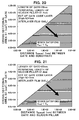
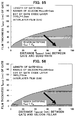
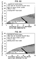
- the following conditional formula (2-2) representing a relationship of the cross-sectional area S1 of the gate 210, and the distance T space1 between the gate 210 and the semiconductor substrate 100, is obtained (unit in the formulas (2-2): nm) ( FIG.
- the parasitic capacitance C ov2 between the gate 210 and the second silicon pillar 820 is less than the gate capacitance C g , as shown in the following formula (2-3): C ov ⁇ 2 ⁇ C g
- C ov2 becomes less than C g in a region on the side of the arrowed direction.
- FIG. 15 is a schematic bird's-eye view showing a transistor in a semiconductor device according to the third embodiment of the present invention, wherein the semiconductor device according to the third embodiment is the same as that in the first embodiment, except that the gate oxide layer (first insulating body) 310 made of SiO 2 is replaced by a gate oxide layer 320 made of HfO 2 .
- FIG. 16 is a schematic sectional view taken along the cutting-plane line A-A' in FIG. 15
- FIG. 17 is a top view of the transistor in FIG. 15 .
- FIG. 18 is a schematic sectional view taken along the cutting-plane line B-B' in FIG. 16
- FIG. 19 is a schematic sectional view taken along the cutting-plane line C-C' in FIG.
- the parasitic capacitance C ov1 between the gate 210 and the semiconductor substrate 100 is less than the gate capacitance C g , as shown in the following formula (3-1): C ov ⁇ 1 ⁇ C g
- the length of the gate 210 is 20 nm; the peripheral length of the first silicon pillar 810 is 31.4 nm; the equivalent film thickness T ox of the gate oxide layer 320 is 1 nm; and the interlayer film is made of SiO 2 .
- the following conditional formula (3-2) representing a relationship between the cross-sectional area S1 of the gate 210, and the distance T space1 between the gate 210 and the semiconductor substrate 100, is obtained (unit in the formulas (3-2): nm) ( FIG.
- the parasitic capacitance C vo2 between the gate 210 and the second silicon pillar 820 is less than the gate capacitance C g , as shown in the following formula (3-3): C ov ⁇ 2 ⁇ C g
- the following conditional formula (3-4) representing a relationship between the cross-sectional area S2 of the gate 210, and the distance T space2 between the gate 210 and the second silicon pillar 820, is obtained (unit in the formula (3-4): nm) ( FIG.
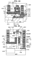
- FIG. 22 is a schematic bird's-eye view showing a transistor in a semiconductor device according to the fourth embodiment of the present invention, wherein the semiconductor device according to the fourth embodiment is the same as that in the first embodiment, except that the interlayer film 610 made of SiO 2 is replaced by an interlayer film 620 made of SiN, and the gate oxide layer 310 made of SiO 2 is replaced by a gate oxide layer 320 made of HfO 2 .
- FIG. 23 is a schematic sectional view taken along the cutting-plane line A-A' in FIG. 22
- FIG. 24 is a top view of the transistor in FIG. 22 .
- FIG. 25 is a schematic sectional view taken along the cutting-plane line B-B' in FIG. 23 , and FIG.
- FIG. 26 is a schematic sectional view taken along the cutting-plane line C-C' in FIG. 23 .
- the parasitic capacitance C ov1 between the gate 210 and the semiconductor substrate 100 is less than the gate capacitance C g , as shown in the following formula (4-1): C ov ⁇ 1 ⁇ C g
- the length of the gate 210 is 20 nm; the peripheral length of the first silicon pillar 810 is 31.4 nm; the equivalent film thickness T ox of the gate oxide layer 320 is 1 nm; and the interlayer film is made of SiN.
- the following conditional formula (4-2) representing a relationship between the cross-sectional area S1 of the gate 210, and the distance T space1 between the gate 210 and the semiconductor substrate 100, is obtained (unit in the formulas (4-2): nm) ( FIG.
- the parasitic capacitance C ov2 between the gate 210 and the second silicon pillar 820 is less than the gate capacitance C g , as shown in the following formula (4-3): C ov ⁇ 2 ⁇ C g
- C ov2 becomes less than C g in a region on the side of the arrowed direction.
- FIG. 29 is a schematic bird's-eye view showing a transistor in a semiconductor device according to the fifth embodiment of the present invention.
- FIG. 30 is a schematic sectional view taken along the cutting-plane line A-A' in FIG. 29
- FIG. 31 is a top view of the transistor in FIG. 29 .
- the semiconductor device according to the fifth embodiment comprises a cross-sectionally circular-shaped first silicon pillar 810 formed on a first-conductive type semiconductor substrate 100, a first insulating body 310 surrounding a part of a surface of the first silicon pillar 810, a gate 210 surrounding the first insulating body 310, and a second silicon pillar 820 formed on a top of the first silicon pillar 810.
- the gate 210 is disposed to be separated from the semiconductor substrate 100 by a second insulating body 610. Further, the gate 210 is disposed to be separated from the second silicon pillar 820 by the second insulating body 610.
- the semiconductor device further comprises a second-conductive type high-concentration impurity region 520 formed in a part of the first silicon pillar 810, a second-conductive type high-concentration impurity region 530 formed in a part of the first silicon pillar 810, a second-conductive type high-concentration impurity region 510 formed in a part of the semiconductor substrate 100, a second-conductive type high-concentration impurity region 540 formed in a part of the second silicon pillar 820, a silicide region 720 formed in a part of the second-conductive type high-concentration impurity region 510, a silicide region 710 formed in the second-conductive type high-concentration impurity region 540, a contact 430 formed on the silicide region 720, a contact 420 formed on the silicide region 710, a contact 410 formed on the gate 210, and an element isolation region 910 formed in the semiconductor substrate 100.
- a parasitic capacitance C ov1 between the gate 210 and the semiconductor substrate 100 is less than a gate capacitance C g , as shown in the following formula (5-1): C ov ⁇ 1 ⁇ C g Specifically, given that: a length of the gate 210 is 20 nm; a diameter of the first silicon pillar 810 is 10 nm; a film thickness T ox of the gate oxide layer 310 is 1 nm; and the interlayer film is made of SiO 2 .
- a relationship of the capacitance C ov1 between the gate 210 and the semiconductor substrate 100, a dielectric constant ⁇ X of the interlayer film 610, a cross-sectional area S1 of the gate 210, and a distance T space1 between the gate 210 and the semiconductor substrate 100, is expressed as the following formula (5-2), and then the formula (5-2) is assigned to the formula (5-1) to obtain the following formula (5-3):
- the gate capacitance C g is expressed as the following formula (5-4) which is a relational expression of a dielectric constant ⁇ 0X of the gate oxide layer 310, the length 1 of the gate 210, a radius R of the first silicon pillar 810, and the film thickness T ox of the gate oxide layer 310, and the cross-sectional area S1 of the gate 210 is expressed as the following formula (5-5) which is a relational expression of a gate film thickness T gate1 of a first one of opposite ends of the gate, the radius R of the first silicon pillar 810 and the film thickness T ox of the gate oxide layer 310.
- the peripheral length of the first silicon pillar 810 is set in the range of 1 nm to 100 ⁇ m, and the film thickness of the gate oxide layer 310 is set in the range of 0.5 to 100 nm. Further, the length of the gate 210 is set in the range of 5 nm to 10 ⁇ m, and the dielectric constant ⁇ X of the interlayer film is set in the range of 3.9 to 7.6. In this structure, conditions satisfying the formula (5-1) will be calculated. Given that: the peripheral length of the first silicon pillar 810 is 100 ⁇ m; the film thickness of the gate oxide layer 310 is 0.5 nm; the length of the gate 210 is 10 ⁇ m, and the dielectric constant ⁇ X of the interlayer film is 3.9.
- the gate capacitance C g is expressed as the following formula (5-8) which is a relational expression of the dielectric constant ⁇ 0X of the gate oxide layer 310, the length 1 of the gate 210, the radius R of the first silicon pillar 810, and the film thickness T ox of the gate oxide layer 310, and the cross-sectional area S 1 of the gate 210 is expressed as the following formula (5-9) which is a relational expression of the gate film thickness T gate1 , the radius R of the first silicon pillar 810 and the film thickness T ox of the gate oxide layer 310.
- a parasitic capacitance C ov2 between the gate 210 and the second silicon pillar 820 is less than the gate capacitance C g , as shown in the following formula (5-13): C ov ⁇ 2 ⁇ C g
- the length of the gate 210 is 20 nm; the diameter of the first silicon pillar 810 is 10 nm; the film thickness T ox of the gate oxide layer 310 is 1 nm; and the interlayer film is made of SiO 2 .
- a relationship of the capacitance C ov2 between the gate 210 and the second silicon pillar 820, the dielectric constant ⁇ X of the interlayer film 610, a cross-sectional area S2 of the gate 210, and a distance T space2 between the gate 210 and the second silicon pillar 820, is expressed as the following formula (5-14), and then the formula (5-14) is assigned to the formula (5-13) to obtain the following formula (5-15):
- the gate capacitance C g is expressed as the following formula (5-16) which is a relational expression of the dielectric constant ⁇ 0X of the gate oxide layer 310, the length 1 of the gate 210, the radius R of the first silicon pillar 810, and the film thickness T ox of the gate oxide layer 310, and the cross-sectional area S2 of the gate 210 is expressed as the following formula (5-17) which is a relational expression of a gate film thickness T gate2 of the other, second end of the gate 210, the radius R of the first silicon pillar 810 and the film thickness T ox of the gate oxide layer 310.
- the peripheral length of the first silicon pillar 810 is set in the range of 1 nm to 100 ⁇ m, and the film thickness of the gate oxide layer 310 is set in the range of 0.5 to 100 nm. Further, the length of the gate 210 is set in the range of 5 nm to 10 ⁇ m, and the dielectric constant ⁇ X of the interlayer film is set in the range of 3.9 to 7.6. In this structure, conditions satisfying the formula (5-13) will be calculated. Given that: the peripheral length of the first silicon pillar 810 is 100 ⁇ m; the film thickness of the gate oxide layer 310 is 0.5 nm; the length of the gate 210 is 10 ⁇ m, and the dielectric constant ⁇ X of the interlayer film is 3.9.
- the gate capacitance C g is expressed as the following formula (5-20) which is a relational expression of the dielectric constant ⁇ 0X of the gate oxide layer 310, the length I of the gate 210, the radius R of the first silicon pillar 810, and the film thickness T ox of the gate oxide layer 310, and the cross-sectional area S2 of the gate 210 is expressed as the following formula (5-21) which is a relational expression of the gate film thickness T gate2 , the radius R of the first silicon pillar 810 and the film thickness T ox of the gate oxide layer 310.
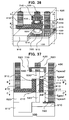
- FIG. 36 is a schematic bird's-eye view showing a transistor in a semiconductor device according to the sixth embodiment of the present invention, wherein the semiconductor device according to the sixth embodiment is the same as that in the fifth embodiment, except that the interlayer film 610 made of SiO 2 is replaced by an interlayer film 620 made of SiN.
- FIG. 37 is a schematic sectional view taken along the cutting-plane line A-A' in FIG. 36
- FIG. 38 is a top view of the transistor in FIG. 36
- FIG. 39 is a schematic sectional view taken along the cutting-plane line B-B' in FIG. 37
- FIG. 40 is a schematic sectional view taken along the cutting-plane line C-C' in FIG. 37 .
- the parasitic capacitance C ov1 between the gate 210 and the semiconductor substrate 100 is less than the gate capacitance C g , as shown in the following formula (6-1): C ov ⁇ 1 ⁇ C g
- the length of the gate 210 is 20 nm; the diameter of the first silicon pillar 810 is 10 nm; and the film thickness T ox of the gate oxide layer 310 made of SiO 2 is 1.0 nm.
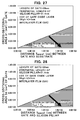
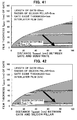
- the following conditional formula (6-2) representing a relationship between the film thickness T gate1 of the gate 210, and the distance T spacet1 between the gate 210 and the semiconductor substrate 100, is obtained (unit in the formulas (6-2): nm) ( FIG.
- the parasitic capacitance C ov2 between the gate 210 and the second silicon pillar 820 is less than the gate capacitance C g , as shown in the following formula (6-3): C ov ⁇ 2 ⁇ C g
- the following conditional formula (6-4) representing a relationship between the film thickness T gate2 of the gate 210, and the distance T space2 between the gate 210 and the second silicon pillar 820, is obtained (unit in the formula (6-4): nm) ( FIG.
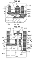
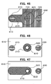
- FIG. 43 is a schematic bird's-eye view showing a transistor in a semiconductor device according to the seventh embodiment of the present invention, wherein the semiconductor device according to the seventh embodiment is the same as that in the fifth embodiment, except that the gate oxide layer 310 made of SiO 2 is replaced by a gate oxide layer 320 made of HfO 2 .
- FIG. 44 is a schematic sectional view taken along the cutting-plane line A-A' in FIG. 43
- FIG. 45 is a top view of the transistor in FIG. 43 .
- FIG. 46 is a schematic sectional view taken along the cutting-plane line B-B' in FIG. 44
- FIG. 47 is a schematic sectional view taken along the cutting-plane line C-C' in FIG. 44 .
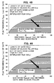
- the parasitic capacitance C ov1 between the gate 210 and the semiconductor substrate 100 is less than the gate capacitance C g , as shown in the following formula (7-1): C ov ⁇ 1 ⁇ C g
- the length of the gate 210 is 20 nm; the diameter of the first silicon pillar 810 is 10 nm; and the film thickness T ox of the gate oxide layer 320 made of HfO 2 is 1.3 nm (equivalent oxide thickness (EOT)).
- EOT equivalent oxide thickness
- the parasitic capacitance C ov2 between the gate 210 and the second silicon pillar 820 is less than the gate capacitance C g , as shown in the following formula (7-3): C ov ⁇ 2 ⁇ C g
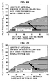
- conditional formula (7-4) representing a relationship between the film thickness T gate2 of the gate 210, and the distance T space2 between the gate 210 and the second silicon pillar 820, is obtained (unit in the formula (7-4): nm) ( FIG. 49 ): 5.4 ⁇ e ⁇ 2 ⁇ T space ⁇ 2 ⁇ ⁇ ⁇ 10 + T gate ⁇ 2 2 - 3.3 ⁇ e ⁇ 2 ⁇ C ov ⁇ 2 ⁇ C g
- C ov2 becomes less than C g in a region on the side of the arrowed direction.
- FIG. 50 is a schematic bird's-eye view showing a transistor in a semiconductor device according to the eighth embodiment of the present invention, wherein the semiconductor device according to the eighth embodiment is the same as that in the fifth embodiment, except that the interlayer film 610 made of SIO 2 is replaced by an interlayer film 620 made of SiN, and the gate oxide layer 310 made of SiO 2 is replaced by a gate oxide layer 320 made of HfO 2 .
- FIG. 51 is a schematic sectional view taken along the cutting-plane line A-A' in FIG. 50
- FIG. 52 is a top view of the transistor in FIG. 50 .
- FIG. 53 is a schematic sectional view taken along the cutting-plane line B-B' in FIG. 51
- the parasitic capacitance C ov1 between the gate 210 and the semiconductor substrate 100 is less than the gate capacitance C g , as shown in the following formula (8-1): C ov ⁇ 1 ⁇ C g
- the length of the gate 210 is 20 nm; the diameter of the first silicon pillar 810 is 10 nm; and the film thickness T ox of the gate oxide layer 320 made of HfO 2 is 1.3 nm (EOT).
- the following conditional formula (8-2) representing a relationship between the film thickness T gace1 of the gate 210, and the distance T space1 between the gate 210 and the semiconductor substrate 100, is obtained (unit in the formulas (8-2): nm) ( FIG.
- the parasitic capacitance C ov2 between the gate 210 and the second silicon pillar 820 is less than the gate capacitance C g , as shown in the following formula (8-3): C ov ⁇ 2 ⁇ C g
- conditional formula (8-4) representing a relationship between the film thickness T gate2 of the gate 210, and the distance T space2 between the gate 210 and the second silicon pillar 820, is obtained (unit in the formula (8-4): nm) ( FIG. 56 ): 2.8 ⁇ e ⁇ 2 ⁇ T space ⁇ 2 ⁇ ⁇ ⁇ 10 + T gate ⁇ 2 2 - 3.3 ⁇ e ⁇ 2 ⁇ C ov ⁇ 2 ⁇ C g
- C ov2 becomes less than C g in a region on the side of the arrowed direction.
- FIG. 57 is a schematic bird's-eye view showing a transistor in a semiconductor device according to the ninth embodiment of the present invention.
- FIG. 58 is a schematic sectional view taken along the cutting-plane line A-A' in FIG. 57
- FIG. 59 is a top view of the transistor in FIG. 57 .
- the semiconductor device comprises a cross-sectionally square-shaped first silicon pillar 810 formed on a first-conductive type semiconductor substrate 100, a first insulating body 310 surrounding a part of a surface of the first silicon pillar 810, a gate 210 surrounding the first insulating body 310, and a second silicon pillar 820 formed on a top of the first silicon pillar 810.
- the gate 210 is disposed to be separated from the semiconductor substrate 100 by a second insulating body 610. Further, the gate 210 is disposed to be separated from the second silicon pillar 820 by the second insulating body 610.
- the semiconductor device further comprises a second-conductive type high-concentration impurity region 520 formed in a part of the first silicon pillar 810, a second-conductive type high-concentration impurity region 530 formed in a part of the first silicon pillar 810, a second-conductive type high-concentration impurity region 510 formed in a part of the semiconductor substrate 100, a second-conductive type high-concentration impurity region 540 formed in a part of the second silicon pillar 820, a silicide region 720 formed in a part of the second-conductive type high-concentration impurity region 510, a silicide region 710 formed in the second-conductive type high-concentration impurity region 540, a contact 430 formed on the silicide region 720, a contact 420 formed on the silicide region 710, a contact 410 formed on the gate 210, and an element isolation region 910 formed in the semiconductor substrate 100.
- a parasitic capacitance C ov1 between the gate 210 and the semiconductor substrate 100 is less than a gate capacitance C g , as shown in the following formula (9-1): C ov ⁇ 1 ⁇ C g
- a length of the gate 210 is 20 nm; one side of the first silicon pillar 810 is 10 nm; a film thickness T ox of the gate oxide layer 310 is 1 nm; and the interlayer film is made of SiO 2 .
- the gate capacitance C g is expressed as the following formula (9-4) which is a relational expression of a dielectric constant ⁇ 0X of the gate oxide layer 310, the length I of the gate 210, a length R of one side of the first silicon pillar 810, and the film thickness T ox of the gate oxide layer 310, and the cross-sectional area S 1 of the gate 210 is expressed as the following formula (9-5).
- the formulas (9-4) and (9-5) are assigned to the formula (9-1) to obtain the following conditional formula (9-6) representing a relationship between the cross-sectional area S1 of the gate 210, and the distance T space1 between the gate 210 and the semiconductor substrate 100:
- the length of one side of the first silicon pillar 810 is set in the range of 0.25 nm to 25 ⁇ m, and the film thickness of the gate oxide layer 310 is set in the range of 0.5 to 100 nm. Further, the length of the gate 210 is set in the range of 5 nm to 10 ⁇ m, and the dielectric constant ⁇ X of the interlayer film is set in the range of 3.9 to 7.6. In this structure, conditions satisfying the formula (9-1) will be calculated.
- the length R of one side of the first silicon pillar 810 is 25 ⁇ m; the film thickness of the gate oxide layer 310 is 0.5 nm; the length of the gate 210 is 10 ⁇ m, and the dielectric constant ⁇ X of the interlayer film is 3.9.
- the gate capacitance C g is expressed as the following formula (9-8) which is a relational expression of the dielectric constant ⁇ 0X of the gate oxide layer 310, the length I of the gate 210, the length R of one side of the first silicon pillar 810, and the film thickness T ox of the gate oxide layer 310, and the cross-sectional area S1 of the gate 210 is expressed as the following formula (9-9).
- a parasitic capacitance C ov2 between the gate 210 and the second silicon pillar 820 is less than the gate capacitance C g , as shown in the following formula (9-13): C ov ⁇ 2 ⁇ C g
- the length of the gate 210 is 20 nm; one side of the first silicon pillar 810 is 10 nm; the film thickness T ox of the gate oxide layer 310 is 1 nm; and the interlayer film is made of SiO 2 .
- a relationship of the capacitance C ov2 between the gate 210 and the second silicon pillar 820, the dielectric constant ⁇ X of the interlayer film 610, a cross-sectional area S2 of the gate 210, and a distance T space2 between the gate 210 and the second silicon pillar 820, is expressed as the following formula (9-14), and then the formula (9-14) is assigned to the formula (9-13) to obtain the following formula (9-15):
- C ov ⁇ 2 ⁇ x ⁇ S ⁇ 2 T space ⁇ 2
- the gate capacitance C g is expressed as the following formula (9-16) which is a relational expression of the dielectric constant ⁇ 0X of the gate oxide layer 310, the length 1 of the gate 210, a peripheral length w of the first silicon pillar 810, and the film thickness T ox of the gate oxide layer 310, and the cross-sectional area S2 of the gate 210 is expressed as the following formula (9-17).
- the formulas (9-16) and (9-17) are assigned to the formula (9-13) to obtain the following conditional formula (9-18) representing a relationship between the cross-sectional area S2 of the gate 210, and the distance T space2 between the gate 210 and the second silicon pillar 820:
- the length of one side of the first silicon pillar 810 is set in the range of 0.25 nm to 25 ⁇ m, and the film thickness of the gate oxide layer 310 is set in the range of 0.5 to 100 nm. Further, the length of the gate 210 is set in the range of 5 nm to 10 ⁇ m, and the dielectric constant ⁇ X of the interlayer film is set in the range of 3.9 to 7.6. In this structure, conditions satisfying the formula (9-1) will be calculated. Given that: the peripheral length of the first silicon pillar 810 is 25 ⁇ m; the film thickness of the gate oxide layer 310 is 0.5 nm; the length of the gate 210 is 10 ⁇ m, and the dielectric constant ⁇ X of the interlayer film is 3.9.
- the gate capacitance C g is expressed as the following formula (9-20) which is a relational expression of the dielectric constant ⁇ 0X of the gate oxide layer 310, the length 1 of the gate 210, the peripheral length w of the first silicon pillar 810, and the film thickness T ox of the gate oxide layer 310, and the cross-sectional area S2 of the gate 210 is expressed as the following formula (9-21).
- the formulas (9-20) and (9-21) are assigned to the formula (9-13) to obtain the following conditional formula (9-22) representing a relationship between the cross-sectional area S2 of the gate 210, and the distance T space2 between the gate 210 and the second silicon pillar 820:
- FIG. 64 is a schematic bird's-eye view showing a transistor in a semiconductor device according to the tenth embodiment of the present invention, wherein the semiconductor device according to the tenth embodiment is the same as that in the ninth embodiment, except that the interlayer film 610 made of SiO 2 is replaced by an interlayer film 620 made of SiN.
- FIG. 65 is a schematic sectional view taken along the cutting-plane line A-A' in FIG. 64
- FIG. 66 is a top view of the transistor in FIG. 64 .
- FIG. 67 is a schematic sectional view taken along the cutting-plane line B-B' in FIG. 65
- FIG. 68 is a schematic sectional view taken along the cutting-plane line C-C' in FIG. 65 .
- the parasitic capacitance C ov1 between the gate 210 and the semiconductor substrate 100 is less than the gate capacitance C g , as shown in the following formula (10-1): C ov ⁇ 1 ⁇ C g
- the length of the gate 210 is 20 nm; the length of one side of the first silicon pillar 810 is 10 nm; and the film thickness T ox of the gate oxide layer 310 is 1.0 nm (EOT).
- the following conditional formula (10-2) representing a relationship between the film thickness T gate1 of the gate 210, and the distance T space1 between the gate 210 and the semiconductor substrate 100, is obtained (unit in the formulas (10-2): nm) ( FIG.
- the parasitic capacitance C ov2 between the gate 210 and the second silicon pillar 820 is less than the gate capacitance C g , as shown in the following formula (10-3): C ov ⁇ 2 ⁇ C g
- conditional formula (10-4) representing a relationship between the film thickness T gate2 of the gate 210, and the distance T space2 between the gate 210 and the second silicon pillar 820, is obtained (unit in the formula (10-4): nm) ( FIG. 70 ): 4.1 ⁇ e ⁇ 2 ⁇ T space ⁇ 2 ⁇ 2 ⁇ T gate ⁇ 2 + 12 2 - 1.4 ⁇ e ⁇ 2 ⁇ C ov ⁇ 2 ⁇ C g
- C ov2 becomes less than C g in a region on the side of the arrowed direction.
- FIG. 71 is a schematic bird's-eye view showing a transistor in a semiconductor device according to the eleventh embodiment of the present invention, wherein the semiconductor device according to the eleventh embodiment is the same as that in the ninth embodiment, except that the gate oxide layer 310 made of SiO 2 is replaced by a gate oxide layer 320 made of HfO 2 .
- FIG. 72 is a schematic sectional view taken along the cutting-plane line A-A' in FIG. 71
- FIG. 73 is a top view of the transistor in FIG. 71 .
- FIG. 74 is a schematic sectional view taken along the cutting-plane line B-B' in FIG. 72
- FIG. 75 is a schematic sectional view taken along the cutting-plane line C-C' in FIG.
- the parasitic capacitance C ov1 between the gate 210 and the semiconductor substrate 100 is less than the gate capacitance C g , as shown in the following formula (11-1): C ov ⁇ 1 ⁇ C g
- the length of the gate 210 is 20 nm; the length of one side of the first silicon pillar 810 is 10 nm; and the film thickness T ox of the gate oxide layer 320 made of HfO 2 is 1.3 nm (EOT).
- EOT the film thickness T ox of the gate oxide layer 320 made of HfO 2
- the parasitic capacitance C ov2 between the gate 210 and the second silicon pillar 820 is less than the gate capacitance C g , as shown in the following formula (11-3): C ov ⁇ 2 ⁇ C g
- the following conditional formula (11-4) representing a relationship between the film thickness T gate2 of the gate 210, and the distance T space2 between the gate 210 and the second silicon pillar 820, is obtained (unit in the formula (11-4): nm) ( FIG.
- FIG. 78 is a schematic bird's-eye view showing a transistor in a semiconductor device according to the twelfth embodiment of the present invention, wherein the semiconductor device according to the twelfth embodiment is the same as that in the ninth embodiment, except that the gate oxide layer 310 made of SiO 2 is replaced by a gate oxide layer 320 made of HfO 2 and the interlayer film 610 made of SiO 2 is replaced by an interlayer film 620 made of SiN.
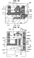
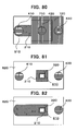
- FIG. 79 is a schematic sectional view taken along the cutting-plane line A-A' in FIG. 78
- FIG. 80 is a top view of the transistor in FIG. 78 .
- FIG. 81 is a schematic sectional view taken along the cutting-plane line B-B' in FIG.
- FIG. 82 is a schematic sectional view taken along the cutting-plane line C-C' in FIG. 79 .
- the parasitic capacitance C ov1 between the gate 210 and the semiconductor substrate 100 is less than the gate capacitance C g , as shown in the following formula (12-1): C ov ⁇ 1 ⁇ C g
- the length of the gate 210 is 20 nm; the length of one side of the first silicon pillar 810 is 10 nm; and the film thickness T ox of the gate oxide layer 320 made of HfO 2 is 1.3 nm (EOT).
- the following conditional formula (12-2) representing a relationship between the film thickness T gate1 of the gate 210, and the distance T space1 between the gate 210 and the semiconductor substrate 100, is obtained (unit in the formulas (12-2): nm) ( FIG.
- the parasitic capacitance C ov2 between the gate 210 and the second silicon pillar 820 is less than the gate capacitance C g , as shown in the following formula (12-3): C ov ⁇ 2 ⁇ C g
- conditional formula (12-4) representing a relationship between the film thickness T gate2 of the gate 210, and the distance T space2 between the gate 210 and the second silicon pillar 820, is obtained (unit in the formula (12-4): nm) ( FIG. 84 ): 2.7 ⁇ e ⁇ 2 ⁇ T space ⁇ 2 ⁇ 2 ⁇ T gate ⁇ 2 + 20 2 - 4.2 ⁇ e ⁇ 2 ⁇ C ov ⁇ 1 ⁇ C g
- C ov2 becomes less than C g in a region on the side of the arrowed direction.
- FIG. 85 is a schematic bird's-eye view showing a transistor in a semiconductor device according to the thirteenth embodiment of the present invention.
- FIG. 86 is a schematic sectional view taken along the cutting-plane line A-A' in FIG. 85
- FIG. 87 is a top view of the transistor in FIG. 85 .
- FIG. 86 is a schematic bird's-eye view showing a transistor in a semiconductor device according to the thirteenth embodiment of the present invention.
- FIG. 86 is a schematic sectional view taken along the cutting-plane line A-A' in FIG. 85
- FIG. 87 is a top view of the transistor in FIG. 85 .
- the semiconductor device according to the thirteenth embodiment comprises a cross-sectionally rectangular-shaped first silicon pillar 810 formed on a first-conductive type semiconductor substrate 100, a first insulating body 310 surrounding a part of a surface of the first silicon pillar 810, a gate 210 surrounding the first insulating body 310, and a second silicon pillar 820 formed on a top of the first silicon pillar 810.
- the gate 210 is disposed to be separated from the semiconductor substrate 100 by a second insulating body 610. Further, the gate 210 is disposed to be separated from the second silicon pillar 820 by the second insulating body 610.
- the semiconductor device further comprises a second-conductive type high-concentration impurity region 520 formed in a part of the first silicon pillar 810, a second-conductive type high-concentration impurity region 530 formed in a part of the first silicon pillar 810, a second-conductive type high-concentration impurity region 510 formed in a part of the semiconductor substrate 100, a second-conductive type high-concentration impurity region 540 formed in a part of the second silicon pillar 820, a silicide region 720 formed in a part of the second-conductive type high-concentration impurity region 510, a silicide region 710 formed in the second-conductive type high-concentration impurity region 540, a contact 430 formed on the silicide region 720, a contact 420 formed on the silicide region 710, a contact 410 formed on the gate 210, and an element isolation region 910 formed in the semiconductor substrate 100.
- a parasitic capacitance C ov1 between the gate 210 and the semiconductor substrate 100 is less than a gate capacitance C g , as shown in the following formula (13-1): C ov ⁇ 1 ⁇ C g
- a length of the gate 210 is 20 nm; a short side and a long side of the first silicon pillar 810 are 10 nm and 20 nm, respectively; a film thickness T ox of the gate oxide layer 310 is 1 nm; and the interlayer film is made of SiO 2 .
- the gate capacitance C g is expressed as the following formula (13-4) which is a relational expression of a dielectric constant ⁇ 0X of the gate oxide layer 310, the length I of the gate 210, respective lengths R, 2R of the short and long sides of the first silicon pillar 810, and the film thickness T ox of the gate oxide layer 310, and the cross-sectional area S 1 of the gate 210 is expressed as the following formula (13-5).
- the length of one side of the first silicon pillar 810 is set in the range of 0.25 nm to 25 ⁇ m, and the film thickness of the gate oxide layer 310 is set in the range of 0.5 to 100 nm.
- the length of the gate 210 is set in the range of 5 nm to 10 ⁇ m, and the dielectric constant ⁇ X of the interlayer film is set in the range of 3.9 to 7.6.
- conditions satisfying the formula (13-1) will be calculated. Given that: the length R of the short side of the first silicon pillar 810 is 25 ⁇ m; the film thickness of the gate oxide layer 310 is 0.5 nm; the length of the gate 210 is 10 ⁇ m, and the dielectric constant ⁇ X of the interlayer film is 3.9.
- the gate capacitance C g is expressed as the following formula (13-8) which is a relational expression of the dielectric constant ⁇ 0X of the gate oxide layer 310, the length 1 of the gate 210, the length R of the short side of the first silicon pillar 810, and the film thickness T ox of the gate oxide layer 310, and the cross-sectional area S1 of the gate 210 is expressed as the following formula (13-9).
- the formulas (13-8) and (13-9) are assigned to the formula (13-3) to obtain the following conditional formula (13-10) representing a relationship between a film thickness T gate1 of the gate 210, and the distance T space1 between the gate 210 and the semiconductor substrate 100:
- a parasitic capacitance C ov2 between the gate 210 and the second silicon pillar 820 is less than the gate capacitance C g , as shown in the following formula (13-13): C ov ⁇ 2 ⁇ C g Specifically, given that: the length of the gate 210 is 20 nm; the length R of the short side of the first silicon pillar 810 is 10 nm; the film thickness T ox of the gate oxide layer 310 is 1 nm; and the interlayer film is made of SiO 2 .
- a relationship of the capacitance C ov2 between the gate 210 and the second silicon pillar 820, the dielectric constant ⁇ X of the interlayer film 610, a cross-sectional area S2 of the gate 210, and a distance T space2 between the gate 210 and the second silicon pillar 820, is expressed as the following formula (13-14), and then the formula (13-14) is assigned to the formula (13-13) to obtain the following formula (13-15):
- the gate capacitance C g is expressed as the following formula (13-16) which is a relational expression of the dielectric constant ⁇ 0x of the gate oxide layer 310, the length 1 of the gate 210, a peripheral length w (6R) of the first silicon pillar 810, and the film thickness T ox of the gate oxide layer 310, and the cross-sectional area S2 of the gate 210 is expressed as the following formula (13-17).
- the formulas (13-16) and (13-17) are assigned to the formula (13-16) to obtain the following conditional formula (13-18) representing a relationship between the cross-sectional area S2 of the gate 210, and the distance T space2 between the gate 210 and the second silicon pillar 820:
- the length of one side of the first silicon pillar 810 is set in the range of 0.25 nm to 25 ⁇ m, and the film thickness of the gate oxide layer 310 is set in the range of 0.5 to 100 nm. Further, the length of the gate 210 is set in the range of 5 nm to 10 ⁇ m, and the dielectric constant ⁇ X of the interlayer film is set in the range of 3.9 to 7.6. In this structure, conditions satisfying the formula (13-1) will be calculated.
- the peripheral length of the first silicon pillar 810 is 25 ⁇ m; the film thickness of the gate oxide layer 310 is 0.5 nm; the length of the gate 210 is 10 ⁇ m, and the dielectric constant ⁇ X of the interlayer film is 3.9.
- the gate capacitance C g is expressed as the following formula (13-20) which is a relational expression of the dielectric constant ⁇ 0X of the gate oxide layer 310, the length 1 of the gate 210, the peripheral length w of the first silicon pillar 810, and the film thickness T ox of the gate oxide layer 310, and the cross-sectional area S2 of the gate 210 is expressed as the following formula (13-21).
- FIG. 92 is a schematic bird's-eye view showing a transistor in a semiconductor device according to the fourteenth embodiment of the present invention, wherein the semiconductor device according to the fourteenth embodiment is the same as that in the thirteenth embodiment, except that the interlayer film 610 made of SiO 2 is replaced by an interlayer film 620 made of SiN.
- FIG. 93 is a schematic sectional view taken along the cutting-plane line A-A' in FIG. 92
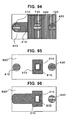
- FIG. 94 is a top view of the transistor in FIG. 92 .
- FIG. 95 is a schematic sectional view taken along the cutting-plane line B-B' in FIG. 93
- FIG. 96 is a schematic sectional view taken along the cutting-plane line C-C' in FIG.
- the parasitic capacitance C ov1 between the gate 210 and the semiconductor substrate 100 is less than the gate capacitance C g , as shown in the following formula (14-1): C ov ⁇ 1 ⁇ C g
- the length of the gate 210 is 20 nm; the short and long sides of the first silicon pillar 810 are 10 nm and 20 nm, respectively; and the film thickness T ox of the gate oxide layer 310 is 1.0 nm (EOT).
- the following conditional formula (14-2) representing a relationship between the film thickness T gate1 of the gate 210, and the distance T space1 between the gate 210 and the semiconductor substrate 100, is obtained (unit in the formulas (14-2): nm) ( FIG.
- the parasitic capacitance C ov2 between the gate 210 and the second silicon pillar 820 is less than the gate capacitance C g , as shown in the following formula (14-3): C ov ⁇ 2 ⁇ C g
- conditional formula (14-4) representing a relationship between the film thickness T gate2 of the gate 210, and the distance T space2 between the gate 210 and the second silicon pillar 820, is obtained (unit in the formula (14-4): nm) ( FIG. 98 ): 6.2 ⁇ e ⁇ 2 ⁇ T space ⁇ 2 ⁇ 4 ⁇ T gate ⁇ 2 2 + 68 ⁇ T gate ⁇ 2 ⁇ C ov ⁇ 2 ⁇ C g
- C ov2 becomes less than C g in a region on the side of the arrowed direction.
- FIG. 99 is a schematic bird's-eye view showing a transistor in a semiconductor device according to the fifteenth embodiment of the present invention, wherein the semiconductor device according to the fifteenth embodiment is the same as that in the thirteenth embodiment, except that the gate oxide layer 310 made of SiO 2 is replaced by a gate oxide layer 320 made of HfO 2 .
- FIG. 100 is a schematic sectional view taken along the cutting-plane line A-A' in FIG. 99
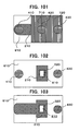
- FIG. 101 is a top view of the transistor in FIG. 99 .
- FIG. 102 is a schematic sectional view taken along the cutting-plane line B-B' in FIG. 100
- FIG. 103 is a schematic sectional view taken along the cutting-plane line C-C' in FIG. 100 .
- the parasitic capacitance C ov1 between the gate 210 and the semiconductor substrate 100 is less than the gate capacitance C g , as shown in the following formula (15-1): C ov ⁇ 1 ⁇ C g
- the length of the gate 210 is 20 nm; the length R of the short side of the first silicon pillar 810 is 10 nm; and the film thickness T ox of the gate oxide layer 320 made of HfO 2 is 1.3 nm (EOT).
- EOT the film thickness T ox of the gate oxide layer 320 made of HfO 2
- C ov1 becomes less than C g in a region on the side of the arrowed direction.
- the parasitic capacitance C ov2 between the gate 210 and the second silicon pillar 820 is less than the gate capacitance C g , as shown in the following formula (15-3): C ov ⁇ 2 ⁇ C g
- conditional formula (15-4) representing a relationship between the film thickness T gate2 of the gate 210, and the distance T space2 between the gate 210 and the second silicon pillar 820, is obtained (unit in the formula (15-4): nm) ( FIG. 105 ): 8.0 ⁇ e ⁇ 2 ⁇ T space ⁇ 2 ⁇ 4 ⁇ T gate ⁇ 2 2 + 1.0 ⁇ e ⁇ 2 ⁇ T gate ⁇ 2 ⁇ C ov ⁇ 2 ⁇ C g
- C ov2 becomes less than C g in a region on the side of the arrowed direction.
- FIG. 106 is a schematic bird's-eye view showing a transistor in a semiconductor device according to the sixteenth embodiment of the present invention, wherein the semiconductor device according to the sixteenth embodiment is the same as that in the thirteenth embodiment, except that the gate oxide layer 310 made of SiO 2 is replaced by a gate oxide layer 320 made of HfO 2 , and the interlayer film 610 made of SiO 2 is replaced by an interlayer film 620 made of SiN.
- FIG. 107 is a schematic sectional view taken along the cutting-plane line A-A' in FIG. 106
- FIG. 108 is a top view of the transistor in FIG. 106 .
- FIG. 109 is a schematic sectional view taken along the cutting-plane line B-B' in FIG.
- FIG. 110 is a schematic sectional view taken along the cutting-plane line C-C' in FIG. 107 .
- the parasitic capacitance C ov1 between the gate 210 and the semiconductor substrate 100 is less than the gate capacitance C g , as shown in the following formula (16-1): C ov ⁇ 1 ⁇ C g
- the length of the gate 210 is 20 nm; the length R of the short side of the first silicon pillar 810 is 10 nm; and the film thickness T ox of the gate oxide layer 320 made of HfO 2 is 1.3 nm (EOT).
- EOT the film thickness T ox of the gate oxide layer 320 made of HfO 2
- C ov1 becomes less than C g in a region on the side of the arrowed direction.
- the parasitic capacitance C ov2 between the gate 210 and the second silicon pillar 820 is less than the gate capacitance C g , as shown in the following formula (16-3): C ov ⁇ 2 ⁇ C g
- the following conditional formula (16-4) representing a relationship between the film thickness T gate2 of the gate 210, and the distance T space2 between the gate 210 and the second silicon pillar 820, is obtained (unit in the formula (16-4): nm) ( FIG.
- the present invention provides a semiconductor device which comprises a second-conductive type impurity region formed in a part of a first-conductive type semiconductor substrate, a first silicon pillar of an arbitrary cross-sectional shape formed on the second-conductive type impurity region, a first insulating body surrounding a part of a surface of the first silicon pillar, a gate surrounding the first insulating body, and a second silicon pillar which is formed on the first silicon pillar and which includes a second-conductive type impurity region, wherein: the gate is disposed to be separated from the semiconductor substrate by the first insulating body and is disposed to be separated from the second silicon pillar by a second insulating body; and each of the capacitance between the gate and the semiconductor substrate, and the capacitance between the gate and the second silicon pillar, is less than a gate capacitance.
- the present invention can reduce a parasitic capacitance of a semiconductor device to provide a semiconductor device for a high-speed and low-power consumption ULSI (ultra large
Landscapes
- Insulated Gate Type Field-Effect Transistor (AREA)
- Thin Film Transistor (AREA)
Abstract
Description
- The present invention relates to a semiconductor device, and more specifically to a surrounding gate transistor (SGT) and a production method therefor.
- A miniaturized planar transistor is used in a wide range of fields, such as computers, communication apparatuses, measurement instruments, automatic control units and domestic appliances, as a fundamental element of low-power consumption, low-cost and high-throughput microprocessors, ASICs and microcomputers and low-cost and large-capacity memories. However, the planar transistor is formed on a semiconductor substrate in a planar configuration, i.e., in a configuration where a source, a gate and drain are horizontally arranged along a surface of a silicon substrate. In contrast, an SGT has a structure where a source, a gate and a drain are arranged in a direction perpendicular to a silicon substrate, and wherein the gate is disposed to surround a convex-shaped semiconductor layer (see, for example, the following
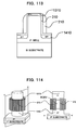
Non-Patent Document 1;FIG. 113 ). Thus, as compared with the planar transistor, the SGT is capable of significantly reducing a transistor occupancy area. However, in a conventional SGT structure, along with the progress in reducing the scale of the SGT structure, an area ratio of a gate electrode to a total transistor occupancy area becomes larger. In addition, due to reducing the scale of a silicon pillar, a resistance in each of source and drain regions formed in the silicon pillar is increased, and thereby an ON current is reduced. - For this reason, a buried-gate SGT (BG-SGT) has been proposed which has an SGT structure where a gate is buried in a silicon pillar (see, for example, the following Non-Patent
Document 2;FIG. 114 ). In this structure, a silicon pillar can be formed to have a small-diameter channel region and large-diameter source and drain regions, so as to simultaneously meet a need for suppressing short-channel effects and a need for reducing a resistance in each of the source and drain regions, i.e., achieve a reduction in OFF-current and an increase in ON-current.
However, as regards to a need for ensuring a low parasitic capacitance to achieve an increase in speed and power consumption reduction in an LSI circuit, the conventional BG-SGT is incapable of achieving such a low parasitic capacitance between the gate and the source or between the gate and the drain. - In this connection, as a technique for reducing a gate-drain parasitic capacitance and a gate-source parasitic capacitance to achieve an increase in speed of the circuit, a vertical replacement gate (VRG)-MOSFET has been known (see, for example, the following
Non-Patent Document 3 andPatent Document 1;FIG. 115 ) and other techniques (see, for example, the followingPatent Document 2;FIG. 116 ).
FIG. 115 shows the VRG-MOSFET (the Patent Document 1). A gate adjacent a silicon pillar faces not only a silicon pillar through a gate oxide layer but also each of a source region and a drain region through an interlayer insulating film. Thus, in addition to a gate capacitance between the gate and the silicon pillar, parasitic capacitances are produced between the gate and the source and between the gate and the drain, respectively. A structure proposed here is intended to increase a film thickness of the interlayer insulating film between the gate and the source to increase a distance therebetween and increase a film thickness of the interlayer insulating film between the gate and the drain to increase a distance therebetween, so as to reduce the respective parasitic capacitances. -
FIG. 116 shows an SGT having a structure intended to reduce a parasitic capacitance between a gate and a source, as disclosed in thePatent Document 2. A gate adjacent a silicon pillar faces not only a silicon pillar through a gate oxide layer but also a source region through an interlayer insulating film. Thus, in addition to a gate capacitance between the gate and the silicon pillar, a parasitic capacitance is produced between the gate and the source. A structure proposed here is intended to increase a film thickness of the interlayer insulating film between the gate and the source to increase a distance between the gate and the source, so as to reduce the parasitic capacitance. -
- Non-Patent Document 1: H. Takato et al, IEEE transaction on electron devices, Vol. 38, No. 3, March 1991, p 573-578
- Non-Patent Document 2: M. Iwai et al, Extended Abstracts of the 2003 International Conference on Solid State Devices and Materials, Tokyo, 2003, p 630-631
- Non-Patent Document 3: IEDM 1999 John M. Hergenrother
- Patent Document 1:
U.S. Patent No. 6,027,975 (Feb. 22, 2000, John M. Hergenrother ) - Patent Document 2:
U.S. Patent No. 5,504,359 (Apr. 2, 1996, Mark S. Rodder ) - In order to allow an SGT constituting an LST to actually achieve an increase in speed thereof, it is desirable that a parasitic capacitance be less than a gate capacitance. Although the SGT structure (such as the Patent Document 2) is intended to reduce a parasitic capacitance by a technique capable of reducing the parasitic capacitance as compared with the conventional structure (such as the Non-Patent Document 1), it may be assumed that the resulting parasitic capacitance is not less than a gate capacitance, or not sufficiently less than a gate capacitance. In the
Patent Document 1 where the thickness of the interlayer film between the gate and the source is increased to reduce the parasitic capacitance as compared with the conventional structure, there is a problem that a parasitic capacitance less than a gate capacitance cannot be obtained without reducing an area of the gate facing the source region. In thePatent Document 2 where the thickness of the interlayer film between the gate and the source is greater than a thickness of the gate oxide film, there is also a problem that a parasitic capacitance less than a gate capacitance cannot be obtained without reducing an area of the gate facing the source region.
In view of the above problems, it is an object of the present invention to provide a semiconductor device designed to reduce a parasitic capacitance to solve the problem of reduction in operating speed of an SGT. - In order to achieve the above object, according to a first aspect of the present invention, there is provided a semiconductor device which comprises: a second-conductive type impurity region formed in a part of a first-conductive type semiconductor substrate; a first silicon pillar of an arbitrary cross-sectional shape formed on the second-conductive type impurity region; a first insulating body surrounding a part of a surface of the first silicon pillar; a gate surrounding the first insulating body; and a second silicon pillar which is formed on the first silicon pillar and which includes a second-conductive type impurity region, wherein: the gate is disposed to be separated from the semiconductor substrate by the first insulating body and is disposed to be separated from the second silicon pillar by a second insulating body; and the capacitance between the gate and the semiconductor substrate is less than a gate capacitance, and the capacitance between the gate and the second silicon pillar is less than the gate capacitance.
- Preferably, the capacitance between the gate and the semiconductor substrate is sufficiently less than the gate capacitance, and the capacitance between the gate and the second silicon pillar is sufficiently less than the gate capacitance.
- Preferably, a cross-sectional area (unit: nm2) of the gate is less than the value derived by multiplying a distance (unit: nm) between the gate and the semiconductor substrate separated by the second insulating body, by 2×10⁹, and is less than the value derived by multiplying a distance (unit: nm) between the gate and the second silicon pillar separated by the second insulating body, by 2×10⁹.
- In another embodiment of the present invention, the first silicon pillar is comprised of a cross-sectionally circular-shaped silicon pillar, and each of the first insulating body surrounding the part of the surface of the first silicon pillar and the gate surrounding the first insulating body has a cross-sectionally circular ring shape.
In this case, the thickness Tgate1 (unit: µm) of one of opposite ends of the gate, and a distance Tspace1 (unit: µm) between the gate and the semiconductor substrate separated by the second insulating body, satisfy the following relational expression:
and
the thickness Tgate2 (unit: µm) of the other end of the gate and a distance Tspace2 (unit: µm) between the gate and the second silicon pillar separated by the second insulating body satisfy the following relational expression:
The one end and the other end of the gate may be a semiconductor substrate-side end and a second silicon pillar-side end of the gate, respectively. - In yet another embodiment of the present invention, the first silicon pillar is comprised of a cross-sectionally square-shaped silicon pillar, and each of the first insulating body surrounding the part of the surface of the first silicon pillar and the gate surrounding the first insulating body has a cross-sectionally square shape.
In this case, the thickness Tgate1 (unit: µm) of one of opposite ends of the gate and a distance Tspace1 (unit: µm) between the gate and the semiconductor substrate separated by the second insulating body satisfy the following relational expression:
and
the thickness Tgate2 (unit: µm) of the other end of the gate and a distance Tspace2 (unit: µm) between the gate and the second silicon pillar separated by the second insulating body satisfy the following relational expression:
- In still another embodiment of the present invention, the first silicon pillar is comprised of a cross-sectionally rectangular-shaped silicon pillar and each of the first insulating body surrounding the part of the surface of the first silicon pillar, and the gate surrounding the first insulating body has a cross-sectionally rectangular shape.
In this case, the thickness Tgate1 (unit: µm) of one of opposite ends of the gate and a distance Tspace1 (unit: µm) between the gate and the semiconductor substrate separated by the second insulating body satisfy the following relational expression:
and
the thickness Tgate2 (unit: µm) of the other end of the gate and a distance Tspace2 (unit: µm) between the gate and the second silicon pillar separated by the second insulating body satisfy the following relational expression:
- In a preferred embodiment of the present invention, the second insulating body may be made of SiO2 or SiN, or has a layered structure of SiO2 and SiN.
The first insulating body may be made of one selected from the group consisting of SiO2, HfO2, and SiON.
The gate may be made of a material selected from the group consisting of TaN, TiN, NiSi, Ni3Si, Ni2Si, PtSi, Pt3Si, and W. - In a preferred embodiment of the present invention, the first silicon pillar may include a second-conductive type high-concentration impurity region adjacent the second-conductive type impurity region formed in the part of the semiconductor substrate, and a second-conductive type high-concentration impurity region adjacent the second silicon pillar.
The semiconductor device may further comprise a second-conductive type high-concentration impurity region formed in a part of the second silicon pillar.
The semiconductor device may further comprise a silicide region formed in a part of the second-conductive type impurity region formed in the part of the semiconductor substrate, and a silicide region formed in a part of a second-conductive type high-concentration impurity region of the second silicon pillar. - The present invention can reduce a parasitic capacitance of a semiconductor device to provide a semiconductor device for a high-speed and low-power consumption ULSI (ultra large-scale integration) circuit.
- With reference to the drawings, a semiconductor device of the present invention will now be specifically described. As shown in the following Table, first to sixteen embodiments are different from each other in at least one of a cross-sectional shape of a first silicon pillar, a material of a second insulating body (interlayer film), and a material of a first insulating body (gate oxide layer).
Embodiment Cross-sectional shape of first silicon pillar Second insulating body (interlayer film) 610, 620 First insulating body (gate oxide layer) 310, 320 FIGS. 1 Arbitrary shape SiO2 SiO2 1 - 7 2 SiN SiO2 8 - 14 3 SiO2 HfO2 15 - 21 4 SiN HfO2 22 - 28 5 Circular shape SiO2 SiO2 29 - 35 6 SiN SiO2 36 - 42 7 SiO2 HfO2 43 - 49 8 SiN HfO2 50 - 56 9 Square shape SiO2 SiO2 57 - 63 10 SiN SiO2 64 - 70 11 SiO2 HfO2 71 - 77 12 SiN HfO2 78 - 84 13 Rectangular shape SiO2 SiO2 85 - 91 14 SiN SiO2 92 - 98 15 SiO2 HfO2 99 - 105 16 SiN HfO2 106 - 112 - Each of first to fourth embodiments of the present invention is an example where a
first silicon pillar 810 has an arbitrary shape in cross-section.FIG. 1 is a schematic bird's-eye view showing a transistor in a semiconductor device according to the first embodiment of the present invention.FIG. 2 is a schematic sectional view taken along the cutting-plane line A-A' inFIG. 1 , andFIG. 3 is a top view of the transistor inFIG. 1 .FIG. 4 is a schematic sectional view taken along the cutting-plane line B-B' inFIG. 2 , andFIG. 5 is a schematic sectional view taken along the cutting-plane line C-C' inFIG. 2 . The semiconductor device according to the first embodiment comprises afirst silicon pillar 810 of an arbitrary cross-sectional shape formed on a first-conductivetype semiconductor substrate 100, a firstinsulating body 310 surrounding a part of a surface of thefirst silicon pillar 810, agate 210 surrounding the firstinsulating body 310, and asecond silicon pillar 820 formed on a top of thefirst silicon pillar 810. Thegate 210 is disposed to be separated from thesemiconductor substrate 100 by a secondinsulating body 610. Further, thegate 210 is disposed to be separated from thesecond silicon pillar 820 by the secondinsulating body 610. - The semiconductor device further comprises a second-conductive type high-
concentration impurity region 520 formed in a part of thefirst silicon pillar 810, a second-conductive type high-concentration impurity region 530 formed in a part of thefirst silicon pillar 810, a second-conductive type high-concentration impurity region 510 formed in a part of thesemiconductor substrate 100, a second-conductive type high-concentration impurity region 540 formed in a part of thesecond silicon pillar 820, asilicide region 720 formed in a part of the second-conductive type high-concentration impurity region 510, asilicide region 710 formed in the second-conductive type high-concentration impurity region 540, acontact 430 formed on thesilicide region 720, acontact 420 formed on thesilicide region 710, acontact 410 formed on thegate 210, and anelement isolation region 910 formed in thesemiconductor substrate 100. Thus, thefirst silicon pillar 810 includes the high-concentration impurity region 520 and the high-concentration impurity region 530. Thesecond silicon pillar 820 includes the high-concentration impurity region 540 and thesilicide region 710. The first insulating body 310 (gate oxide layer) is made of SiO2 and the second insulating body 610 (interlayer film) is made of SiO2. - In order to reduce a parasitic capacitance in the first embodiment, it is desirable that a parasitic capacitance Cov1 between the
gate 210 and thesemiconductor substrate 100 is less than a gate capacitance Cg, as shown in the following formula (1-1):
Specifically, given that: a length of thegate 210 is 20 nm; a peripheral length of thefirst silicon pillar 810 is 31.4 nm; an equivalent film thickness Tox of thegate oxide layer 310 is 1 nm; and the interlayer film is made of SiO2. A relationship of the capacitance Cov1 between thegate 210 and thesemiconductor substrate 100, a dielectric constant εX of theinterlayer film 610, a cross-sectional area S1 of a first one of opposite ends of thegate 210, and a distance Tspace1 between thegate 210 and thesemiconductor substrate 100, is expressed as the following formula (1-2), and then the formula (1-2) is assigned to the formula (1-1) to obtain the following formula (1-3):

- The gate capacitance Cg is expressed as the following formula (1-4) which is a relational expression of a dielectric constant ε0X of SiO2 which is a material of the
gate oxide layer 310, thelength 1 of thegate 210, the peripheral length w of thefirst silicon pillar 810, and the equivalent film thickness Tox of thegate oxide layer 310, and then the formula (1-4) is assigned to the formula (1-3) to obtain the following conditional formula (1-5) representing a relationship between the cross-sectional area S1 of thegate 210, and the distance Tspace1 between thegate 210 and the semiconductor substrate 100:

As used herein, the term "gate capacitance" means the capacitance between two electrodes made up of thegate 210 and thefirst silicon pillar 810 through thegate oxide layer 310 interposed therebetween. - If the conditional formula (1-5) is satisfied, the formula (1-1) is satisfied. Thus, the following formula (1-6) is obtained (unit in the formulas (1-5) and (1-6): nm) (
Fig. 6 ):
- Typically, the peripheral length of the
first silicon pillar 810 is set in the range of 1 nm to 100 µm, and the equivalent film thickness of thegate oxide layer 310 is set in the range of 0.5 to 100 nm, because an SiO2 film or a high-dielectric constant film is used as thegate oxide layer 310. Further, the length of thegate 210 is set in the range of 5 nm to 10 µm, and the dielectric constant εX of the interlayer film is set in the range of 3.8 to 7.6, because the interlayer film is made of SiO2 or SiN. In this structure, conditions satisfying the formula (1-1) will be calculated. Given that: the peripheral length of thefirst silicon pillar 810 is 100 µm; the film thickness of thegate oxide layer 310 is 0.5 nm; the length of thegate 210 is 10 µm, and the dielectric constant εX of the interlayer film is 3.9. The gate capacitance Cg is expressed as the following formula (1-8) which is a relational expression of the dielectric constant ε0X of SiO2 whichis a material of thegate oxide layer 310, thelength 1 of thegate 210, the peripheral length w of thefirst silicon pillar 810, and the equivalent film thickness Tox of thegate oxide layer 310, and then the formula (1-8) is assigned to the formula (1-3) to obtain the following conditional formula (1-9) representing a relationship between the cross-sectional area S1 of thegate 210, and the distance Tspace1 between thegate 210 and the semiconductor substrate 100: -


, wherein 2e9 is 2 × 10⁹. - If the conditional formula (1-9) is satisfied, the formula (1-1) is satisfied. Thus, the following formula (1-10) is obtained, and then the following formula (1-11) is obtained from the formula (1-10) (unit in the formulas (1-9), (1-10) and (1-11): nm):


InFIG. 6 , Cov1 becomes less than Cg in a region on the side of the arrowed direction. - Further, in order to reduce the parasitic capacitance in the first embodiment, it is desirable that a parasitic capacitance Cov2 between the
gate 210 and thesecond silicon pillar 820 is less than the gate capacitance Cg, as shown in the following formula (1-12):
- Specifically, given that: the length of the
gate 210 is 20 nm; the peripheral length of thefirst silicon pillar 810 is 31.4 nm; the equivalent film thickness Tox of thegate oxide layer 310 is 1 nm; and the interlayer film is made of SiO2. A relationship of the capacitance Cov2 between thegate 210 and thesecond silicon pillar 820, the dielectric constant εX of theinterlayer film 610, a cross-sectional area S2 of the other, second, end of thegate 210, and a distance Tspace2 between thegate 210 and thesecond silicon pillar 820, is expressed as the following formula (1-13), and then the formula (1-13) is assigned to the formula (1-12) to obtain the following formula (1-14):

- The gate capacitance Cg is expressed as the following formula (1-15) which is a relational expression of the dielectric constant ε0X of SiO2 as a material of the
gate oxide layer 310, thelength 1 of thegate 210, the peripheral length w of thefirst silicon pillar 810, and the equivalent film thickness Tox of thegate oxide layer 310, and then the formula (1-15) is assigned to the formula (1-14) to obtain the following conditional formula (1-16) representing a relationship of the cross-sectional area S2 of thegate 210, and the distance Tspace2 between thegate 210 and the second silicon pillar 820 (unit in the formula (1-16): nm) (FIG. 7 ):

- Typically, the peripheral length of the
first silicon pillar 810 is set in the range of 1 nm to 100 µm, and the equivalent film thickness of thegate oxide layer 310 is set in the range of 0.5 to 100 nm, because an SiO2 film or a high-dielectric constant film is used as thegate oxide layer 310. Further, the length of thegate 210 is set in the range of 5 nm to 10 µm, and the dielectric constant εX of the interlayer film is set in the range of 3.8 to 7.6, because the interlayer film is made of SiO2 or SiN. In this structure, conditions satisfying the formula (1-12) will be calculated. Given that: the peripheral length of thefirst silicon pillar 810 is 100 µm; the film thickness of thegate oxide layer 310 is 0.5 nm; the length of thegate 210 is 10 µm, and the dielectric constant εX of the interlayer film is 3.9. The gate capacitance Cg is expressed as the following formula (1-17) which is a relational expression of the dielectric constant ε0X of SiO2 as a material of thegate oxide layer 310, thelength 1 of thegate 210, the peripheral length w of thefirst silicon pillar 810, and the equivalent film thickness Tox of thegate oxide layer 310, and then the formula (1-17) is assigned to the formula (1-14) to obtain the following conditional formula (1-18) representing a relationship of the cross-sectional area S2 of thegate 210, and the distance Tspace2 between thegate 210 and the second silicon pillar 820: -


- If the conditional formula (1-18) is satisfied, the formula (1-12) is satisfied. Thus, the following formula (1-19) is obtained, and then the following formula (1-20) is obtained from the formula (1-19) (unit in the formulas (1-18), (1-19) and (1-20): nm):


InFIG. 7 , Cov2 becomes less than Cg in a region on the side of the arrowed direction. -
FIG. 8 is a schematic bird's-eye view showing a transistor in a semiconductor device according to the second embodiment of the present invention, wherein the semiconductor device according to the second embodiment is the same as that in the first embodiment, except that the interlayer film (second insulating body) 610 made of SiO2 is replaced by aninterlayer film 620 made of SiN.FIG. 9 is a schematic sectional view taken along the cutting-plane line A-A' inFIG. 8 , andFIG. 10 is a top view of the transistor inFIG. 8 .FIG. 11 is a schematic sectional view taken along the cutting-plane line B-B' inFIG. 9 , andFIG. 12 is a schematic sectional view taken along the cutting-plane line C-C' inFIG. 9 . As with the first embodiment, in order to reduce a parasitic capacitance in the second embodiment, it is desirable that the parasitic capacitance Cov1 between thegate 210 and thesemiconductor substrate 100 is less than the gate capacitance Cg, as shown in the following

- Specifically, given that: the length of the
gate 210 is 20 nm; the peripheral length of thefirst silicon pillar 810 is 31.4 nm; the equivalent film thickness Tox of thegate oxide layer 310 is 1 nm; and the interlayer film is made of SiN. Based on the formula (1-5) in the first embodiment, the following conditional formula (2-2) representing a relationship of the cross-sectional area S1 of thegate 210, and the distance Tspace1 between thegate 210 and thesemiconductor substrate 100, is obtained (unit in the formulas (2-2): nm) (FIG. 13 ):
InFIG. 13 , Cov1 becomes less than Cg in a region on the side of the arrowed direction. - Further, as with the first embodiment, in order to reduce the parasitic capacitance in the second embodiment where the
interlayer film 620 is made of SiN, instead of SiO2, it is desirable that the parasitic capacitance Cov2 between thegate 210 and thesecond silicon pillar 820 is less than the gate capacitance Cg, as shown in the following formula (2-3):
- Based on the formula (1-16) in the first embodiment, the following conditional formula (2-4) representing a relationship between the cross-sectional area S2 of the
gate 210, and the distance Tspace2 between thegate 210 and thesecond silicon pillar 820, is obtained (unit in the formula (2-4): nm (FIG. 14 ):
InFIG. 14 , Cov2 becomes less than Cg in a region on the side of the arrowed direction. -
FIG. 15 is a schematic bird's-eye view showing a transistor in a semiconductor device according to the third embodiment of the present invention, wherein the semiconductor device according to the third embodiment is the same as that in the first embodiment, except that the gate oxide layer (first insulating body) 310 made of SiO2 is replaced by agate oxide layer 320 made of HfO2.FIG. 16 is a schematic sectional view taken along the cutting-plane line A-A' inFIG. 15 , andFIG. 17 is a top view of the transistor inFIG. 15 .FIG. 18 is a schematic sectional view taken along the cutting-plane line B-B' inFIG. 16 , andFIG. 19 is a schematic sectional view taken along the cutting-plane line C-C' inFIG. 16 . As with the first embodiment, in order to reduce a parasitic capacitance in the third embodiment, it is desirable that the parasitic capacitance Cov1 between thegate 210 and thesemiconductor substrate 100 is less than the gate capacitance Cg, as shown in the following formula (3-1):
- Specifically, given that: the length of the
gate 210 is 20 nm; the peripheral length of thefirst silicon pillar 810 is 31.4 nm; the equivalent film thickness Tox of thegate oxide layer 320 is 1 nm; and the interlayer film is made of SiO2. Based on the formula (1-5) in the first embodiment, the following conditional formula (3-2) representing a relationship between the cross-sectional area S1 of thegate 210, and the distance Tspace1 between thegate 210 and thesemiconductor substrate 100, is obtained (unit in the formulas (3-2): nm) (FIG. 20 ):
InFIG. 20 , Cov1 becomes less than Cg in a region on the side of the arrowed direction. - Further, as with the first embodiment, in order to reduce the parasitic capacitance in the third embodiment where the
interlayer film 610 is made of SiO2 and thegate oxide layer 320 is made of HfO2, it is desirable that the parasitic capacitance Cvo2 between thegate 210 and thesecond silicon pillar 820 is less than the gate capacitance Cg, as shown in the following formula (3-3):
Based on the formula (1-16) in the first embodiment, the following conditional formula (3-4) representing a relationship between the cross-sectional area S2 of thegate 210, and the distance Tspace2 between thegate 210 and thesecond silicon pillar 820, is obtained (unit in the formula (3-4): nm) (FIG. 21 ):
InFIG. 21 , Cov2 becomes less than Cg in a region on the side of the arrowed direction. -
FIG. 22 is a schematic bird's-eye view showing a transistor in a semiconductor device according to the fourth embodiment of the present invention, wherein the semiconductor device according to the fourth embodiment is the same as that in the first embodiment, except that theinterlayer film 610 made of SiO2 is replaced by aninterlayer film 620 made of SiN, and thegate oxide layer 310 made of SiO2 is replaced by agate oxide layer 320 made of HfO2.FIG. 23 is a schematic sectional view taken along the cutting-plane line A-A' inFIG. 22 , andFIG. 24 is a top view of the transistor inFIG. 22 .FIG. 25 is a schematic sectional view taken along the cutting-plane line B-B' inFIG. 23 , andFIG. 26 is a schematic sectional view taken along the cutting-plane line C-C' inFIG. 23 . As with the first embodiment, in order to reduce a parasitic capacitance in the fourth embodiment, it is desirable that the parasitic capacitance Cov1 between thegate 210 and thesemiconductor substrate 100 is less than the gate capacitance Cg, as shown in the following formula (4-1):
- Specifically, given that: the length of the
gate 210 is 20 nm; the peripheral length of thefirst silicon pillar 810 is 31.4 nm; the equivalent film thickness Tox of thegate oxide layer 320 is 1 nm; and the interlayer film is made of SiN. Based on the formula (1-5) in the first embodiment, the following conditional formula (4-2) representing a relationship between the cross-sectional area S1 of thegate 210, and the distance Tspace1 between thegate 210 and thesemiconductor substrate 100, is obtained (unit in the formulas (4-2): nm) (FIG. 27 ):
InFIG. 27 , Cov1 becomes less than Cg in a region on the side of the arrowed direction. - Further, as with the first embodiment, in order to reduce the parasitic capacitance in the fourth embodiment where the
interlayer film 620 is made of SiN and thegate oxide layer 320 is made of HfO2, it is desirable that the parasitic capacitance Cov2 between thegate 210 and thesecond silicon pillar 820 is less than the gate capacitance Cg, as shown in the following formula (4-3):
- Based on the formula (1-16) in the first embodiment, the following conditional formula (4-4) representing a relationship between the cross-sectional area S2 of the
gate 210, and the distance Tspace2 between thegate 210 and thesecond silicon pillar 820, is obtained (unit in the formula (4-4): nm) (FIG. 28 ):
InFIG. 28 , Cov2 becomes less than Cg in a region on the side of the arrowed direction. - Each of fifth to eighth embodiments of the present invention is an example where a
first silicon pillar 810 has a circular shape in cross-section.
In the fifth embodiment, an after-mentioned first insulating body 310 (gate oxide layer) is made of SiO2, and an after-mentioned second insulating body 610 (interlayer film) is made of SiO2.
FIG. 29 is a schematic bird's-eye view showing a transistor in a semiconductor device according to the fifth embodiment of the present invention.FIG. 30 is a schematic sectional view taken along the cutting-plane line A-A' inFIG. 29 , andFIG. 31 is a top view of the transistor inFIG. 29 .FIG. 32 is a schematic sectional view taken along the cutting-plane line B-B' inFIG. 30 , andFIG. 33 is a schematic sectional view taken along the cutting-plane line C-C' inFIG. 30 . The semiconductor device according to the fifth embodiment comprises a cross-sectionally circular-shapedfirst silicon pillar 810 formed on a first-conductivetype semiconductor substrate 100, a firstinsulating body 310 surrounding a part of a surface of thefirst silicon pillar 810, agate 210 surrounding the firstinsulating body 310, and asecond silicon pillar 820 formed on a top of thefirst silicon pillar 810. Thegate 210 is disposed to be separated from thesemiconductor substrate 100 by a secondinsulating body 610. Further, thegate 210 is disposed to be separated from thesecond silicon pillar 820 by the secondinsulating body 610. - The semiconductor device further comprises a second-conductive type high-
concentration impurity region 520 formed in a part of thefirst silicon pillar 810, a second-conductive type high-concentration impurity region 530 formed in a part of thefirst silicon pillar 810, a second-conductive type high-concentration impurity region 510 formed in a part of thesemiconductor substrate 100, a second-conductive type high-concentration impurity region 540 formed in a part of thesecond silicon pillar 820, asilicide region 720 formed in a part of the second-conductive type high-concentration impurity region 510, asilicide region 710 formed in the second-conductive type high-concentration impurity region 540, acontact 430 formed on thesilicide region 720, acontact 420 formed on thesilicide region 710, acontact 410 formed on thegate 210, and anelement isolation region 910 formed in thesemiconductor substrate 100. - In order to reduce a parasitic capacitance in the fifth embodiment, it is desirable that a parasitic capacitance Cov1 between the
gate 210 and thesemiconductor substrate 100 is less than a gate capacitance Cg, as shown in the following formula (5-1):
Specifically, given that: a length of thegate 210 is 20 nm; a diameter of thefirst silicon pillar 810 is 10 nm; a film thickness Tox of thegate oxide layer 310 is 1 nm; and the interlayer film is made of SiO2. A relationship of the capacitance Cov1 between thegate 210 and thesemiconductor substrate 100, a dielectric constant εX of theinterlayer film 610, a cross-sectional area S1 of thegate 210, and a distance Tspace1 between thegate 210 and thesemiconductor substrate 100, is expressed as the following formula (5-2), and then the formula (5-2) is assigned to the formula (5-1) to obtain the following formula (5-3): -


- The gate capacitance Cg is expressed as the following formula (5-4) which is a relational expression of a dielectric constant ε0X of the
gate oxide layer 310, thelength 1 of thegate 210, a radius R of thefirst silicon pillar 810, and the film thickness Tox of thegate oxide layer 310, and the cross-sectional area S1 of thegate 210 is expressed as the following formula (5-5) which is a relational expression of a gate film thickness Tgate1 of a first one of opposite ends of the gate, the radius R of thefirst silicon pillar 810 and the film thickness Tox of thegate oxide layer 310. Thus, the formulas (5-4) and (5-5) are assigned to the formula (5-3) to obtain the following conditional formula (5-6) representing a relationship between the cross-sectional area S1 of thegate 210, and the distance Tspace1 between thegate 210 and the semiconductor substrate 100: -


- If the conditional formula (5-6) is satisfied, the formula (5-1) is satisfied. Thus, the following formula (5-7) is obtained (unit in the formula (5-7: nm) (
FIG. 34 ):
- Typically, the peripheral length of the
first silicon pillar 810 is set in the range of 1 nm to 100 µm, and the film thickness of thegate oxide layer 310 is set in the range of 0.5 to 100 nm. Further, the length of thegate 210 is set in the range of 5 nm to 10 µm, and the dielectric constant εX of the interlayer film is set in the range of 3.9 to 7.6. In this structure, conditions satisfying the formula (5-1) will be calculated. Given that: the peripheral length of thefirst silicon pillar 810 is 100 µm; the film thickness of thegate oxide layer 310 is 0.5 nm; the length of thegate 210 is 10 µm, and the dielectric constant εX of the interlayer film is 3.9. The gate capacitance Cg is expressed as the following formula (5-8) which is a relational expression of the dielectric constant ε0X of thegate oxide layer 310, thelength 1 of thegate 210, the radius R of thefirst silicon pillar 810, and the film thickness Tox of thegate oxide layer 310, and thecross-sectional area S 1 of thegate 210 is expressed as the following formula (5-9) which is a relational expression of the gate film thickness Tgate1, the radius R of thefirst silicon pillar 810 and the film thickness Tox of thegate oxide layer 310. Thus, the formulas (5-8) and (5-9) are assigned to the formula (5-1) to obtain the following conditional formula (5-10) representing a relationship between the cross-sectional area S1 of thegate 210, and the distance Tspace1 between thegate 210 and the semiconductor substrate 100:
-


- If the conditional formula (5-10) is satisfied, the formula (5-1) is satisfied. Thus, the following formula (5-11) is obtained, and then the following formula (5-12) is obtained from the formula (5-11) (unit in the formulas (5-11) and (5-12): µm):


InFIG. 34 , Cvo1 becomes less than Cg in a region on the side of the arrowed direction. - Further, in order to reduce the parasitic capacitance in the fifth embodiment, it is desirable that a parasitic capacitance Cov2 between the
gate 210 and thesecond silicon pillar 820 is less than the gate capacitance Cg, as shown in the following formula (5-13):
- Specifically, given that: the length of the
gate 210 is 20 nm; the diameter of thefirst silicon pillar 810 is 10 nm; the film thickness Tox of thegate oxide layer 310 is 1 nm; and the interlayer film is made of SiO2. A relationship of the capacitance Cov2 between thegate 210 and thesecond silicon pillar 820, the dielectric constant εX of theinterlayer film 610, a cross-sectional area S2 of thegate 210, and a distance Tspace2 between thegate 210 and thesecond silicon pillar 820, is expressed as the following formula (5-14), and then the formula (5-14) is assigned to the formula (5-13) to obtain the following formula (5-15): -


- The gate capacitance Cg is expressed as the following formula (5-16) which is a relational expression of the dielectric constant ε0X of the
gate oxide layer 310, thelength 1 of thegate 210, the radius R of thefirst silicon pillar 810, and the film thickness Tox of thegate oxide layer 310, and the cross-sectional area S2 of thegate 210 is expressed as the following formula (5-17) which is a relational expression of a gate film thickness Tgate2 of the other, second end of thegate 210, the radius R of thefirst silicon pillar 810 and the film thickness Tox of thegate oxide layer 310. Thus, the formulas (5-16) and (5-17) are assigned to the formula (5-15) to obtain the following conditional formula (5-18) representing a relationship between the cross-sectional area S2 of thegate 210, and the distance Tspace2 between thegate 210 and the second silicon pillar 820: -


- If the conditional formula (5-18) is satisfied, the formula (5-13) is satisfied. Thus, the following formula (5-19) is obtained (unit in the formulas (5-19): nm (
FIG. 35 ):
- Typically, the peripheral length of the
first silicon pillar 810 is set in the range of 1 nm to 100 µm, and the film thickness of thegate oxide layer 310 is set in the range of 0.5 to 100 nm. Further, the length of thegate 210 is set in the range of 5 nm to 10 µm, and the dielectric constant εX of the interlayer film is set in the range of 3.9 to 7.6. In this structure, conditions satisfying the formula (5-13) will be calculated. Given that: the peripheral length of thefirst silicon pillar 810 is 100 µm; the film thickness of thegate oxide layer 310 is 0.5 nm; the length of thegate 210 is 10 µm, and the dielectric constant εX of the interlayer film is 3.9. The gate capacitance Cg is expressed as the following formula (5-20) which is a relational expression of the dielectric constant ε0X of thegate oxide layer 310, the length I of thegate 210, the radius R of thefirst silicon pillar 810, and the film thickness Tox of thegate oxide layer 310, and the cross-sectional area S2 of thegate 210 is expressed as the following formula (5-21) which is a relational expression of the gate film thickness Tgate2, the radius R of thefirst silicon pillar 810 and the film thickness Tox of thegate oxide layer 310. Thus, the formulas (5-20) and (5-21) are assigned to the formula (5-13) to obtain the following conditional formula (5-22) representing a relationship between the cross-sectional area S2 of thegate 210, and the distance Tspace2 between thegate 210 and the second silicon pillar 820: -



- If the conditional formula (5-22) is satisfied, the formula (5-13) is satisfied. Thus, the following formula (5-23) is obtained, and then the following formula (5-24) is obtained from the formula (5-23) (unit in the formulas (5-23) and (5-24): µm):


InFIG. 35 , Cov2 becomes less than Cg in a region on the side of the arrowed direction. -
FIG. 36 is a schematic bird's-eye view showing a transistor in a semiconductor device according to the sixth embodiment of the present invention, wherein the semiconductor device according to the sixth embodiment is the same as that in the fifth embodiment, except that theinterlayer film 610 made of SiO2 is replaced by aninterlayer film 620 made of SiN.FIG. 37 is a schematic sectional view taken along the cutting-plane line A-A' inFIG. 36 , andFIG. 38 is a top view of the transistor inFIG. 36 .FIG. 39 is a schematic sectional view taken along the cutting-plane line B-B' inFIG. 37 , andFIG. 40 is a schematic sectional view taken along the cutting-plane line C-C' inFIG. 37 . As with the fifth embodiment, in order to reduce a parasitic capacitance in the sixth embodiment, it is desirable that the parasitic capacitance Cov1 between thegate 210 and thesemiconductor substrate 100 is less than the gate capacitance Cg, as shown in the following formula (6-1):
- Specifically, given that: the length of the
gate 210 is 20 nm; the diameter of thefirst silicon pillar 810 is 10 nm; and the film thickness Tox of thegate oxide layer 310 made of SiO2 is 1.0 nm. Based on the formula (5-6) in the fifth embodiment, the following conditional formula (6-2) representing a relationship between the film thickness Tgate1 of thegate 210, and the distance Tspacet1 between thegate 210 and thesemiconductor substrate 100, is obtained (unit in the formulas (6-2): nm) (FIG. 41 ):
InFIG. 41 , Cov1 becomes less than Cg in a region on the side of the arrowed direction. - Further, as with the fifth embodiment, in order to reduce the parasitic capacitance in the sixth embodiment where the
interlayer film 620 is made of SiN, instead of SiO2, it is desirable that the parasitic capacitance Cov2 between thegate 210 and thesecond silicon pillar 820 is less than the gate capacitance Cg, as shown in the following formula (6-3):
Based on the formula (5-18) in the fifth embodiment, the following conditional formula (6-4) representing a relationship between the film thickness Tgate2 of thegate 210, and the distance Tspace2 between thegate 210 and thesecond silicon pillar 820, is obtained (unit in the formula (6-4): nm) (FIG. 42 ):
InFIG. 42 , Cov2 becomes less than Cg in a region on the side of the arrowed direction. -
FIG. 43 is a schematic bird's-eye view showing a transistor in a semiconductor device according to the seventh embodiment of the present invention, wherein the semiconductor device according to the seventh embodiment is the same as that in the fifth embodiment, except that thegate oxide layer 310 made of SiO2 is replaced by agate oxide layer 320 made of HfO2.FIG. 44 is a schematic sectional view taken along the cutting-plane line A-A' inFIG. 43 , andFIG. 45 is a top view of the transistor inFIG. 43 .FIG. 46 is a schematic sectional view taken along the cutting-plane line B-B' inFIG. 44 , andFIG. 47 is a schematic sectional view taken along the cutting-plane line C-C' inFIG. 44 . As with the fifth embodiment, in order to reduce a parasitic capacitance in the seventh embodiment, it is desirable that the parasitic capacitance Cov1 between thegate 210 and thesemiconductor substrate 100 is less than the gate capacitance Cg, as shown in the following formula (7-1):
- Specifically, given that: the length of the
gate 210 is 20 nm; the diameter of thefirst silicon pillar 810 is 10 nm; and the film thickness Tox of thegate oxide layer 320 made of HfO2 is 1.3 nm (equivalent oxide thickness (EOT)). Based on the formula (5-6) in the fifth embodiment, the following conditional formula (7-2) representing a relationship between the film thickness Tgate1 of thegate 210, and the distance Tspace1 between thegate 210 and thesemiconductor substrate 100, is obtained (unit in the formulas (7-2): nm) (FIG. 48 ):
InFIG. 48 , Cov1 becomes less than Cg in a region on the side of the arrowed direction. - Further, as with the fifth embodiment, in order to reduce the parasitic capacitance in the seventh embodiment where the
gate oxide layer 320 is made of HfO2, instead of SiO2, it is desirable that the parasitic capacitance Cov2 between thegate 210 and thesecond silicon pillar 820 is less than the gate capacitance Cg, as shown in the following formula (7-3):
- Based on the formula (5-18) in the fifth embodiment, the following conditional formula (7-4) representing a relationship between the film thickness Tgate2 of the
gate 210, and the distance Tspace2 between thegate 210 and thesecond silicon pillar 820, is obtained (unit in the formula (7-4): nm) (FIG. 49 ):
InFIG. 49 , Cov2 becomes less than Cg in a region on the side of the arrowed direction. -
FIG. 50 is a schematic bird's-eye view showing a transistor in a semiconductor device according to the eighth embodiment of the present invention, wherein the semiconductor device according to the eighth embodiment is the same as that in the fifth embodiment, except that theinterlayer film 610 made of SIO2 is replaced by aninterlayer film 620 made of SiN, and thegate oxide layer 310 made of SiO2 is replaced by agate oxide layer 320 made of HfO2.FIG. 51 is a schematic sectional view taken along the cutting-plane line A-A' inFIG. 50 , andFIG. 52 is a top view of the transistor inFIG. 50 .FIG. 53 is a schematic sectional view taken along the cutting-plane line B-B' inFIG. 51 , andFIG. 54 is a schematic sectional view taken along the cutting-plane line C-C' inFIG. 51 . As with the fifth embodiment, in order to reduce a parasitic capacitance in the eighth embodiment, it is desirable that the parasitic capacitance Cov1 between thegate 210 and thesemiconductor substrate 100 is less than the gate capacitance Cg, as shown in the following formula (8-1):
- Specifically, given that: the length of the
gate 210 is 20 nm; the diameter of thefirst silicon pillar 810 is 10 nm; and the film thickness Tox of thegate oxide layer 320 made of HfO2 is 1.3 nm (EOT). Based on the formula (5-6) in the fifth embodiment, the following conditional formula (8-2) representing a relationship between the film thickness Tgace1 of thegate 210, and the distance Tspace1 between thegate 210 and thesemiconductor substrate 100, is obtained (unit in the formulas (8-2): nm) (FIG. 55 ):
InFIG. 55 , Cov1 becomes less than Cg in a region on the side of the arrowed direction. - Further, as with the fifth embodiment, in order to reduce the parasitic capacitance in the seventh embodiment where the
interlayer film 620 is made of SiN, instead of SiO2, and thegate oxide layer 320 is made of HfO2, instead of SiO2, it is desirable that the parasitic capacitance Cov2 between thegate 210 and thesecond silicon pillar 820 is less than the gate capacitance Cg, as shown in the following formula (8-3):
- Based on the formula (5-18) in the fifth embodiment, the following conditional formula (8-4) representing a relationship between the film thickness Tgate2 of the
gate 210, and the distance Tspace2 between thegate 210 and thesecond silicon pillar 820, is obtained (unit in the formula (8-4): nm) (FIG. 56 ):
InFIG. 56 , Cov2 becomes less than Cg in a region on the side of the arrowed direction. - Each of ninth to twelfth embodiments of the present invention is an example where a
first silicon pillar 810 has a square shape in cross-section.
In the ninth embodiment, an after-mentioned first insulating body 310 (gate oxide layer) is made of SiO2, and an after-mentioned second insulating body 610 (interlayer film) is made of SiO2.FIG. 57 is a schematic bird's-eye view showing a transistor in a semiconductor device according to the ninth embodiment of the present invention.FIG. 58 is a schematic sectional view taken along the cutting-plane line A-A' inFIG. 57 , andFIG. 59 is a top view of the transistor inFIG. 57 .FIG. 60 is a schematic sectional view taken along the cutting-plane line B-B' inFIG. 58 , andFIG. 61 is a schematic sectional view taken along the cutting-plane line C-C' inFIG. 58 . The semiconductor device according to the ninth embodiment comprises a cross-sectionally square-shapedfirst silicon pillar 810 formed on a first-conductivetype semiconductor substrate 100, a firstinsulating body 310 surrounding a part of a surface of thefirst silicon pillar 810, agate 210 surrounding the firstinsulating body 310, and asecond silicon pillar 820 formed on a top of thefirst silicon pillar 810. Thegate 210 is disposed to be separated from thesemiconductor substrate 100 by a secondinsulating body 610. Further, thegate 210 is disposed to be separated from thesecond silicon pillar 820 by the secondinsulating body 610. - The semiconductor device further comprises a second-conductive type high-
concentration impurity region 520 formed in a part of thefirst silicon pillar 810, a second-conductive type high-concentration impurity region 530 formed in a part of thefirst silicon pillar 810, a second-conductive type high-concentration impurity region 510 formed in a part of thesemiconductor substrate 100, a second-conductive type high-concentration impurity region 540 formed in a part of thesecond silicon pillar 820, asilicide region 720 formed in a part of the second-conductive type high-concentration impurity region 510, asilicide region 710 formed in the second-conductive type high-concentration impurity region 540, acontact 430 formed on thesilicide region 720, acontact 420 formed on thesilicide region 710, acontact 410 formed on thegate 210, and anelement isolation region 910 formed in thesemiconductor substrate 100. - In order to reduce a parasitic capacitance in the ninth embodiment, it is desirable that a parasitic capacitance Cov1 between the
gate 210 and thesemiconductor substrate 100 is less than a gate capacitance Cg, as shown in the following formula (9-1):
- Specifically, given that: a length of the
gate 210 is 20 nm; one side of thefirst silicon pillar 810 is 10 nm; a film thickness Tox of thegate oxide layer 310 is 1 nm; and the interlayer film is made of SiO2. A relationship of the capacitance Cov1 between thegate 210 and thesemiconductor substrate 100, a dielectric constant εX of theinterlayer film 610, a cross-sectional area S1 of thegate 210, and a distance Tspace1 between thegate 210 and thesemiconductor substrate 100, is expressed as the following formula (9-2), and then the formula (9-2) is assigned to the formula (9-1) to obtain the following formula (9-3):

- The gate capacitance Cg is expressed as the following formula (9-4) which is a relational expression of a dielectric constant ε0X of the
gate oxide layer 310, the length I of thegate 210, a length R of one side of thefirst silicon pillar 810, and the film thickness Tox of thegate oxide layer 310, and thecross-sectional area S 1 of thegate 210 is expressed as the following formula (9-5). Thus, the formulas (9-4) and (9-5) are assigned to the formula (9-1) to obtain the following conditional formula (9-6) representing a relationship between the cross-sectional area S1 of thegate 210, and the distance Tspace1 between thegate 210 and the semiconductor substrate 100: -


- If the conditional formula (9-6) is satisfied, the formula (9-1) is satisfied. Thus, the above values are assigned to the formula (9-6) to obtain the following formula (9-7) (unit in the formula (9-7): nm) (
FIG. 62 ):
- Typically, the length of one side of the
first silicon pillar 810 is set in the range of 0.25 nm to 25 µm, and the film thickness of thegate oxide layer 310 is set in the range of 0.5 to 100 nm. Further, the length of thegate 210 is set in the range of 5 nm to 10 µm, and the dielectric constant εX of the interlayer film is set in the range of 3.9 to 7.6. In this structure, conditions satisfying the formula (9-1) will be calculated. Given that: the length R of one side of thefirst silicon pillar 810 is 25 µm; the film thickness of thegate oxide layer 310 is 0.5 nm; the length of thegate 210 is 10 µm, and the dielectric constant εX of the interlayer film is 3.9. The gate capacitance Cg is expressed as the following formula (9-8) which is a relational expression of the dielectric constant ε0X of thegate oxide layer 310, the length I of thegate 210, the length R of one side of thefirst silicon pillar 810, and the film thickness Tox of thegate oxide layer 310, and the cross-sectional area S1 of thegate 210 is expressed as the following formula (9-9). Thus, the formulas (9-8) and (9-9) are assigned to the formula (9-3) to obtain the following conditional formula (9-10) representing a relationship between a film thickness Tgate1 of thegate 210, and the distance Tspace1 between thegate 210 and the semiconductor substrate 100: -


- If the conditional formula (9-10) is satisfied, the formula (9-1) is satisfied. Thus, the above values are assigned to the formula (9-10) to obtain the following formula (9-11), and then the following formula (9-12) is obtained from the formula (9-11) (unit in the formulas (9-11) and (9-12): µm):


InFIG. 62 , Cov1 becomes less than Cg in a region on the side of the arrowed direction. - Further, in order to reduce the parasitic capacitance in the ninth embodiment, it is desirable that a parasitic capacitance Cov2 between the
gate 210 and thesecond silicon pillar 820 is less than the gate capacitance Cg, as shown in the following formula (9-13):
- Specifically, given that: the length of the
gate 210 is 20 nm; one side of thefirst silicon pillar 810 is 10 nm; the film thickness Tox of thegate oxide layer 310 is 1 nm; and the interlayer film is made of SiO2. A relationship of the capacitance Cov2 between thegate 210 and thesecond silicon pillar 820, the dielectric constant εX of theinterlayer film 610, a cross-sectional area S2 of thegate 210, and a distance Tspace2 between thegate 210 and thesecond silicon pillar 820, is expressed as the following formula (9-14), and then the formula (9-14) is assigned to the formula (9-13) to obtain the following formula (9-15):

- The gate capacitance Cg is expressed as the following formula (9-16) which is a relational expression of the dielectric constant ε0X of the
gate oxide layer 310, thelength 1 of thegate 210, a peripheral length w of thefirst silicon pillar 810, and the film thickness Tox of thegate oxide layer 310, and the cross-sectional area S2 of thegate 210 is expressed as the following formula (9-17). Thus, the formulas (9-16) and (9-17) are assigned to the formula (9-13) to obtain the following conditional formula (9-18) representing a relationship between the cross-sectional area S2 of thegate 210, and the distance Tspace2 between thegate 210 and the second silicon pillar 820: -


- If the conditional formula (9-18) is satisfied, the formula (9-13) is satisfied. Thus, the above values are assigned to the formula (9-18) to obtain the following formula (9-19) (unit in the formulas (9-19): nm (
FIG. 63 ):
- Typically, the length of one side of the
first silicon pillar 810 is set in the range of 0.25 nm to 25 µm, and the film thickness of thegate oxide layer 310 is set in the range of 0.5 to 100 nm. Further, the length of thegate 210 is set in the range of 5 nm to 10 µm, and the dielectric constant εX of the interlayer film is set in the range of 3.9 to 7.6. In this structure, conditions satisfying the formula (9-1) will be calculated. Given that: the peripheral length of thefirst silicon pillar 810 is 25 µm; the film thickness of thegate oxide layer 310 is 0.5 nm; the length of thegate 210 is 10 µm, and the dielectric constant εX of the interlayer film is 3.9. The gate capacitance Cg is expressed as the following formula (9-20) which is a relational expression of the dielectric constant ε0X of thegate oxide layer 310, thelength 1 of thegate 210, the peripheral length w of thefirst silicon pillar 810, and the film thickness Tox of thegate oxide layer 310, and the cross-sectional area S2 of thegate 210 is expressed as the following formula (9-21). Thus, the formulas (9-20) and (9-21) are assigned to the formula (9-13) to obtain the following conditional formula (9-22) representing a relationship between the cross-sectional area S2 of thegate 210, and the distance Tspace2 between thegate 210 and the second silicon pillar 820: -


- If the conditional formula (9-22) is satisfied, the formula (9-13) is satisfied. Thus, the above values are assigned to the formula (9-22) to obtain the following formula (9-23), and then the following formula (9-24) is obtained from the formula (9-23) (unit in the formulas (9-23) and (9-24): µm):


InFIG. 63 , Cov2 becomes less than Cg in a region on the side of the arrowed direction. -
FIG. 64 is a schematic bird's-eye view showing a transistor in a semiconductor device according to the tenth embodiment of the present invention, wherein the semiconductor device according to the tenth embodiment is the same as that in the ninth embodiment, except that theinterlayer film 610 made of SiO2 is replaced by aninterlayer film 620 made of SiN.FIG. 65 is a schematic sectional view taken along the cutting-plane line A-A' inFIG. 64 , andFIG. 66 is a top view of the transistor inFIG. 64 .FIG. 67 is a schematic sectional view taken along the cutting-plane line B-B' inFIG. 65 , andFIG. 68 is a schematic sectional view taken along the cutting-plane line C-C' inFIG. 65 . As with the ninth embodiment, in order to reduce a parasitic capacitance in the tenth embodiment, it is desirable that the parasitic capacitance Cov1 between thegate 210 and thesemiconductor substrate 100 is less than the gate capacitance Cg, as shown in the following formula (10-1):
- Specifically, given that: the length of the
gate 210 is 20 nm; the length of one side of thefirst silicon pillar 810 is 10 nm; and the film thickness Tox of thegate oxide layer 310 is 1.0 nm (EOT). Based on the formula (9-6) in the ninth embodiment, the following conditional formula (10-2) representing a relationship between the film thickness Tgate1 of thegate 210, and the distance Tspace1 between thegate 210 and thesemiconductor substrate 100, is obtained (unit in the formulas (10-2): nm) (FIG. 69 ):
InFIG. 69 , Cov1 becomes less than Cg in a region on the side of the arrowed direction. - Further, as with the ninth embodiment, in order to reduce the parasitic capacitance in the tenth embodiment where the
interlayer film 620 is made of SiN, instead of SiO2, it is desirable that the parasitic capacitance Cov2 between thegate 210 and thesecond silicon pillar 820 is less than the gate capacitance Cg, as shown in the following formula (10-3):
- Based on the formula (9-18) in the ninth embodiment, the following conditional formula (10-4) representing a relationship between the film thickness Tgate2 of the
gate 210, and the distance Tspace2 between thegate 210 and thesecond silicon pillar 820, is obtained (unit in the formula (10-4): nm) (FIG. 70 ):
InFIG. 70 , Cov2 becomes less than Cg in a region on the side of the arrowed direction. -
FIG. 71 is a schematic bird's-eye view showing a transistor in a semiconductor device according to the eleventh embodiment of the present invention, wherein the semiconductor device according to the eleventh embodiment is the same as that in the ninth embodiment, except that thegate oxide layer 310 made of SiO2 is replaced by agate oxide layer 320 made of HfO2.FIG. 72 is a schematic sectional view taken along the cutting-plane line A-A' inFIG. 71 , andFIG. 73 is a top view of the transistor inFIG. 71 .FIG. 74 is a schematic sectional view taken along the cutting-plane line B-B' inFIG. 72 , andFIG. 75 is a schematic sectional view taken along the cutting-plane line C-C' inFIG. 72 . As with the ninth embodiment, in order to reduce a parasitic capacitance in the eleventh embodiment, it is desirable that the parasitic capacitance Cov1 between thegate 210 and thesemiconductor substrate 100 is less than the gate capacitance Cg, as shown in the following formula (11-1):
- Specifically, given that: the length of the
gate 210 is 20 nm; the length of one side of thefirst silicon pillar 810 is 10 nm; and the film thickness Tox of thegate oxide layer 320 made of HfO2 is 1.3 nm (EOT). Based on the formula (9-6) in the ninth embodiment, the following conditional formula (11-2) representing a relationship between the film thickness Tgate1 of thegate 210, and the distance Tspace1 between thegate 210 and thesemiconductor substrate 100, is obtained (unit in the formulas (11-2): nm) (FIG. 76 ):
InFIG. 76 , Cov1 becomes less than Cg in a region on the side of the arrowed direction. - Further, as with the ninth embodiment, in order to reduce the parasitic capacitance in the eleventh embodiment where the
gate oxide layer 320 is made of HfO2, instead of SiO2, it is desirable that the parasitic capacitance Cov2 between thegate 210 and thesecond silicon pillar 820 is less than the gate capacitance Cg, as shown in the following formula (11-3):
Based on the formula (9-18) in the ninth embodiment, the following conditional formula (11-4) representing a relationship between the film thickness Tgate2 of thegate 210, and the distance Tspace2 between thegate 210 and thesecond silicon pillar 820, is obtained (unit in the formula (11-4): nm) (FIG. 77 ):
InFIG. 77 , Cov2 becomes less than Cg in a region on the side of the arrowed direction. -
FIG. 78 is a schematic bird's-eye view showing a transistor in a semiconductor device according to the twelfth embodiment of the present invention, wherein the semiconductor device according to the twelfth embodiment is the same as that in the ninth embodiment, except that thegate oxide layer 310 made of SiO2 is replaced by agate oxide layer 320 made of HfO2 and theinterlayer film 610 made of SiO2 is replaced by aninterlayer film 620 made of SiN.FIG. 79 is a schematic sectional view taken along the cutting-plane line A-A' inFIG. 78 , andFIG. 80 is a top view of the transistor inFIG. 78 .FIG. 81 is a schematic sectional view taken along the cutting-plane line B-B' inFIG. 79 , andFIG. 82 is a schematic sectional view taken along the cutting-plane line C-C' inFIG. 79 . As with the ninth embodiment, in order to reduce a parasitic capacitance in the twelfth embodiment, it is desirable that the parasitic capacitance Cov1 between thegate 210 and thesemiconductor substrate 100 is less than the gate capacitance Cg, as shown in the following formula (12-1):
- Specifically, given that: the length of the
gate 210 is 20 nm; the length of one side of thefirst silicon pillar 810 is 10 nm; and the film thickness Tox of thegate oxide layer 320 made of HfO2 is 1.3 nm (EOT). Based on the formula (9-6) in the ninth embodiment, the following conditional formula (12-2) representing a relationship between the film thickness Tgate1 of thegate 210, and the distance Tspace1 between thegate 210 and thesemiconductor substrate 100, is obtained (unit in the formulas (12-2): nm) (FIG. 83 ):
InFIG. 83 , Cov1 becomes less than Cg in a region on the side of the arrowed direction. - Further, as with the ninth embodiment, in order to reduce the parasitic capacitance in the twelfth embodiment where the
gate oxide layer 320 is made of HfO2, instead of SiO2 and theinterlayer film 620 is made of SiN, instead of SiO2, it is desirable that the parasitic capacitance Cov2 between thegate 210 and thesecond silicon pillar 820 is less than the gate capacitance Cg, as shown in the following formula (12-3):
- Based on the formula (9-18) in the ninth embodiment, the following conditional formula (12-4) representing a relationship between the film thickness Tgate2 of the
gate 210, and the distance Tspace2 between thegate 210 and thesecond silicon pillar 820, is obtained (unit in the formula (12-4): nm) (FIG. 84 ):
InFIG. 84 , Cov2 becomes less than Cg in a region on the side of the arrowed direction. - Each of thirteenth to sixteenth embodiments of the present invention is an example where a
first silicon pillar 810 has a rectangular shape in cross-section. In the thirteenth embodiment, an after-mentioned first insulating body 310 (gate oxide layer) is made of SiO2, and an after-mentioned second insulating body 610 (interlayer film) is made of SiO2.
FIG. 85 is a schematic bird's-eye view showing a transistor in a semiconductor device according to the thirteenth embodiment of the present invention.FIG. 86 is a schematic sectional view taken along the cutting-plane line A-A' inFIG. 85 , andFIG. 87 is a top view of the transistor inFIG. 85 .FIG. 88 is a schematic sectional view taken along the cutting-plane line B-B' inFIG. 86 , andFIG. 89 is a schematic sectional view taken along the cutting-plane line C-C' inFIG. 86 . The semiconductor device according to the thirteenth embodiment comprises a cross-sectionally rectangular-shapedfirst silicon pillar 810 formed on a first-conductivetype semiconductor substrate 100, a firstinsulating body 310 surrounding a part of a surface of thefirst silicon pillar 810, agate 210 surrounding the firstinsulating body 310, and asecond silicon pillar 820 formed on a top of thefirst silicon pillar 810. Thegate 210 is disposed to be separated from thesemiconductor substrate 100 by a secondinsulating body 610. Further, thegate 210 is disposed to be separated from thesecond silicon pillar 820 by the secondinsulating body 610. - The semiconductor device further comprises a second-conductive type high-
concentration impurity region 520 formed in a part of thefirst silicon pillar 810, a second-conductive type high-concentration impurity region 530 formed in a part of thefirst silicon pillar 810, a second-conductive type high-concentration impurity region 510 formed in a part of thesemiconductor substrate 100, a second-conductive type high-concentration impurity region 540 formed in a part of thesecond silicon pillar 820, asilicide region 720 formed in a part of the second-conductive type high-concentration impurity region 510, asilicide region 710 formed in the second-conductive type high-concentration impurity region 540, acontact 430 formed on thesilicide region 720, acontact 420 formed on thesilicide region 710, acontact 410 formed on thegate 210, and anelement isolation region 910 formed in thesemiconductor substrate 100. - In order to reduce a parasitic capacitance in the thirteenth embodiment, it is desirable that a parasitic capacitance Cov1 between the
gate 210 and thesemiconductor substrate 100 is less than a gate capacitance Cg, as shown in the following formula (13-1):
- Specifically, given that: a length of the
gate 210 is 20 nm; a short side and a long side of thefirst silicon pillar 810 are 10 nm and 20 nm, respectively; a film thickness Tox of thegate oxide layer 310 is 1 nm; and the interlayer film is made of SiO2. A relationship of the capacitance Cvo1 between thegate 210 and thesemiconductor substrate 100, a dielectric constant εX of theinterlayer film 610, a cross-sectional area S1 of thegate 210, and a distance Tspace1 between thegate 210 and thesemiconductor substrate 100, is expressed as the following formula (13-2), and then the formula (13-2) is assigned to the formula (13-1) to obtain the following formula (13-3):

- The gate capacitance Cg is expressed as the following formula (13-4) which is a relational expression of a dielectric constant ε0X of the
gate oxide layer 310, the length I of thegate 210, respective lengths R, 2R of the short and long sides of thefirst silicon pillar 810, and the film thickness Tox of thegate oxide layer 310, and thecross-sectional area S 1 of thegate 210 is expressed as the following formula (13-5). Thus, the formulas (13-4) and (13-5) are assigned to the formula (13-1) to obtain the following conditional formula (13-6) representing a relationship between thecross-sectional area S 1 of thegate 210, and the distance Tspace1 between thegate 210 and the semiconductor substrate 100:


- If the conditional formula (13-6) is satisfied, the formula (13-1) is satisfied. Thus, the above values are assigned to the formula (13-6) to obtain the following formula (13-7) (unit in the formula (13-7): nm) (
FIG. 90 ):
Typically, the length of one side of thefirst silicon pillar 810 is set in the range of 0.25 nm to 25 µm, and the film thickness of thegate oxide layer 310 is set in the range of 0.5 to 100 nm. Further, the length of thegate 210 is set in the range of 5 nm to 10 µm, and the dielectric constant εX of the interlayer film is set in the range of 3.9 to 7.6. In this structure, conditions satisfying the formula (13-1) will be calculated. Given that: the length R of the short side of thefirst silicon pillar 810 is 25 µm; the film thickness of thegate oxide layer 310 is 0.5 nm; the length of thegate 210 is 10 µm, and the dielectric constant εX of the interlayer film is 3.9. The gate capacitance Cg is expressed as the following formula (13-8) which is a relational expression of the dielectric constant ε0X of thegate oxide layer 310, thelength 1 of thegate 210, the length R of the short side of thefirst silicon pillar 810, and the film thickness Tox of thegate oxide layer 310, and the cross-sectional area S1 of thegate 210 is expressed as the following formula (13-9). Thus, the formulas (13-8) and (13-9) are assigned to the formula (13-3) to obtain the following conditional formula (13-10) representing a relationship between a film thickness Tgate1 of thegate 210, and the distance Tspace1 between thegate 210 and the semiconductor substrate 100: -


- If the conditional formula (13-10) is satisfied, the formula (13-1) is satisfied. Thus, the above values are assigned to the formula (13-10) to obtain the following formula (13-11), and then the following formula (13-12) is obtained from the formula (13-11) (unit in the formulas (13-11) and (13-12): µm):


InFIG. 90 , Cov1 becomes less than Cg in a region on the side of the arrowed direction. - Further, in order to reduce the parasitic capacitance in the thirteenth embodiment, it is desirable that a parasitic capacitance Cov2 between the
gate 210 and thesecond silicon pillar 820 is less than the gate capacitance Cg, as shown in the following formula (13-13):
Specifically, given that: the length of thegate 210 is 20 nm; the length R of the short side of thefirst silicon pillar 810 is 10 nm; the film thickness Tox of thegate oxide layer 310 is 1 nm; and the interlayer film is made of SiO2. A relationship of the capacitance Cov2 between thegate 210 and thesecond silicon pillar 820, the dielectric constant εX of theinterlayer film 610, a cross-sectional area S2 of thegate 210, and a distance Tspace2 between thegate 210 and thesecond silicon pillar 820, is expressed as the following formula (13-14), and then the formula (13-14) is assigned to the formula (13-13) to obtain the following formula (13-15): -


- The gate capacitance Cg is expressed as the following formula (13-16) which is a relational expression of the dielectric constant ε0x of the
gate oxide layer 310, thelength 1 of thegate 210, a peripheral length w (6R) of thefirst silicon pillar 810, and the film thickness Tox of thegate oxide layer 310, and the cross-sectional area S2 of thegate 210 is expressed as the following formula (13-17). Thus, the formulas (13-16) and (13-17) are assigned to the formula (13-16) to obtain the following conditional formula (13-18) representing a relationship between the cross-sectional area S2 of thegate 210, and the distance Tspace2 between thegate 210 and the second silicon pillar 820: -


- If the conditional formula (13-18) is satisfied, the formula (13-13) is satisfied. Thus, the above values are assigned to the formula (13-18) to obtain the following formula (13-19) (unit in the formulas (13-19): nm (
FIG. 91 ):
- Typically, the length of one side of the
first silicon pillar 810 is set in the range of 0.25 nm to 25 µm, and the film thickness of thegate oxide layer 310 is set in the range of 0.5 to 100 nm. Further, the length of thegate 210 is set in the range of 5 nm to 10 µm, and the dielectric constant εX of the interlayer film is set in the range of 3.9 to 7.6. In this structure, conditions satisfying the formula (13-1) will be calculated. Given that: the peripheral length of thefirst silicon pillar 810 is 25 µm; the film thickness of thegate oxide layer 310 is 0.5 nm; the length of thegate 210 is 10 µm, and the dielectric constant εX of the interlayer film is 3.9. The gate capacitance Cg is expressed as the following formula (13-20) which is a relational expression of the dielectric constant ε0X of thegate oxide layer 310, thelength 1 of thegate 210, the peripheral length w of thefirst silicon pillar 810, and the film thickness Tox of thegate oxide layer 310, and the cross-sectional area S2 of thegate 210 is expressed as the following formula (13-21). Thus, the formulas (13-20) and (13-21) are assigned to the formula (13-15) to obtain the following conditional formula (13-22) representing a relationship between the cross-sectional area S2 of thegate 210, and the distance Tspace2 between thegate 210 and the second silicon pillar 820: -



- If the conditional formula (13-22) is satisfied, the formula (13-23) is satisfied. Thus, the above values are assigned to the formula (13-22) to obtain the following formula (13-23), and then the following formula (13-24) is obtained from the formula (13-23) (unit in the formulas (13-23) and (13-24): µm):


InFIG. 91 , Cov2 becomes less than Cg in a region on the side of the arrowed direction. -
FIG. 92 is a schematic bird's-eye view showing a transistor in a semiconductor device according to the fourteenth embodiment of the present invention, wherein the semiconductor device according to the fourteenth embodiment is the same as that in the thirteenth embodiment, except that theinterlayer film 610 made of SiO2 is replaced by aninterlayer film 620 made of SiN.FIG. 93 is a schematic sectional view taken along the cutting-plane line A-A' inFIG. 92 , andFIG. 94 is a top view of the transistor inFIG. 92 .FIG. 95 is a schematic sectional view taken along the cutting-plane line B-B' inFIG. 93 , andFIG. 96 is a schematic sectional view taken along the cutting-plane line C-C' inFIG. 93 . As with the thirteenth embodiment, in order to reduce a parasitic capacitance in the fourteenth embodiment, it is desirable that the parasitic capacitance Cov1 between thegate 210 and thesemiconductor substrate 100 is less than the gate capacitance Cg, as shown in the following formula (14-1):
- Specifically, given that: the length of the
gate 210 is 20 nm; the short and long sides of thefirst silicon pillar 810 are 10 nm and 20 nm, respectively; and the film thickness Tox of thegate oxide layer 310 is 1.0 nm (EOT). Based on the formula (13-6) in the thirteenth embodiment, the following conditional formula (14-2) representing a relationship between the film thickness Tgate1 of thegate 210, and the distance Tspace1 between thegate 210 and thesemiconductor substrate 100, is obtained (unit in the formulas (14-2): nm) (FIG. 97 ):
InFIG. 97 , Cov1 becomes less than Cg in a region on the side of the arrowed direction. - Further, as with the thirteenth embodiment, in order to reduce the parasitic capacitance in the fourteenth embodiment where the
interlayer film 620 is made of SiN, instead of SiO2, it is desirable that the parasitic capacitance Cov2 between thegate 210 and thesecond silicon pillar 820 is less than the gate capacitance Cg, as shown in the following formula (14-3):
- Based on the formula (13-18) in the thirteenth embodiment, the following conditional formula (14-4) representing a relationship between the film thickness Tgate2 of the
gate 210, and the distance Tspace2 between thegate 210 and thesecond silicon pillar 820, is obtained (unit in the formula (14-4): nm) (FIG. 98 ):
InFIG. 98 , Cov2 becomes less than Cg in a region on the side of the arrowed direction. -
FIG. 99 is a schematic bird's-eye view showing a transistor in a semiconductor device according to the fifteenth embodiment of the present invention, wherein the semiconductor device according to the fifteenth embodiment is the same as that in the thirteenth embodiment, except that thegate oxide layer 310 made of SiO2 is replaced by agate oxide layer 320 made of HfO2.FIG. 100 is a schematic sectional view taken along the cutting-plane line A-A' inFIG. 99 , andFIG. 101 is a top view of the transistor inFIG. 99 .FIG. 102 is a schematic sectional view taken along the cutting-plane line B-B' inFIG. 100 , andFIG. 103 is a schematic sectional view taken along the cutting-plane line C-C' inFIG. 100 . As with the thirteenth embodiment, in order to reduce a parasitic capacitance in the fifteenth embodiment, it is desirable that the parasitic capacitance Cov1 between thegate 210 and thesemiconductor substrate 100 is less than the gate capacitance Cg, as shown in the following formula (15-1):
- Specifically, given that: the length of the
gate 210 is 20 nm; the length R of the short side of thefirst silicon pillar 810 is 10 nm; and the film thickness Tox of thegate oxide layer 320 made of HfO2 is 1.3 nm (EOT). Based on the formula (13-6) in the thirteenth embodiment, the following conditional formula (15-2) representing a relationship between the film thickness Tgate1 of thegate 210, and the distance Tspace1 between thegate 210 and thesemiconductor substrate 100, is obtained (unit in the formulas (15-2): nm) (FIG. 104 ):
InFIG. 104 , Cov1 becomes less than Cg in a region on the side of the arrowed direction. - Further, as with the thirteenth embodiment, in order to reduce the parasitic capacitance in the fifteenth embodiment where the
gate oxide layer 320 is made of SiN, instead of SiO2, it is desirable that the parasitic capacitance Cov2 between thegate 210 and thesecond silicon pillar 820 is less than the gate capacitance Cg, as shown in the following formula (15-3):
- Based on the formula (13-18) in the thirteenth embodiment, the following conditional formula (15-4) representing a relationship between the film thickness Tgate2 of the
gate 210, and the distance Tspace2 between thegate 210 and thesecond silicon pillar 820, is obtained (unit in the formula (15-4): nm) (FIG. 105 ):
InFIG. 105 , Cov2 becomes less than Cg in a region on the side of the arrowed direction. -
FIG. 106 is a schematic bird's-eye view showing a transistor in a semiconductor device according to the sixteenth embodiment of the present invention, wherein the semiconductor device according to the sixteenth embodiment is the same as that in the thirteenth embodiment, except that thegate oxide layer 310 made of SiO2 is replaced by agate oxide layer 320 made of HfO2, and theinterlayer film 610 made of SiO2 is replaced by aninterlayer film 620 made of SiN.FIG. 107 is a schematic sectional view taken along the cutting-plane line A-A' inFIG. 106 , andFIG. 108 is a top view of the transistor inFIG. 106 .FIG. 109 is a schematic sectional view taken along the cutting-plane line B-B' inFIG. 107 , andFIG. 110 is a schematic sectional view taken along the cutting-plane line C-C' inFIG. 107 . As with the thirteenth embodiment, in order to reduce a parasitic capacitance in the sixteenth embodiment, it is desirable that the parasitic capacitance Cov1 between thegate 210 and thesemiconductor substrate 100 is less than the gate capacitance Cg, as shown in the following formula (16-1):
- Specifically, given that: the length of the
gate 210 is 20 nm; the length R of the short side of thefirst silicon pillar 810 is 10 nm; and the film thickness Tox of thegate oxide layer 320 made of HfO2 is 1.3 nm (EOT). Based on the formula (13-6) in the thirteenth embodiment, the following conditional formula (16-2) representing a relationship between the film thickness Tgate1 of thegate 210, and the distance Tspace1 between thegate 210 and thesemiconductor substrate 100, is obtained (unit in the formulas (16-2): nm) (FIG. 111 ):
InFIG. 111 , Cov1 becomes less than Cg in a region on the side of the arrowed direction. - Further, as with the thirteenth embodiment, in order to reduce the parasitic capacitance in the sixteenth embodiment where the
gate oxide layer 320 is made of SiN, instead of SiO2, and theinterlayer film 620 is made of SiN, instead of SiO2, it is desirable that the parasitic capacitance Cov2 between thegate 210 and thesecond silicon pillar 820 is less than the gate capacitance Cg, as shown in the following formula (16-3):
Based on the formula (13-18) in the thirteenth embodiment, the following conditional formula (16-4) representing a relationship between the film thickness Tgate2 of thegate 210, and the distance Tspace2 between thegate 210 and thesecond silicon pillar 820, is obtained (unit in the formula (16-4): nm) (FIG. 112 ):
InFIG. 112 , Cov2 becomes less than Cg in a region on the side of the arrowed direction. - As above, the present invention provides a semiconductor device which comprises a second-conductive type impurity region formed in a part of a first-conductive type semiconductor substrate, a first silicon pillar of an arbitrary cross-sectional shape formed on the second-conductive type impurity region, a first insulating body surrounding a part of a surface of the first silicon pillar, a gate surrounding the first insulating body, and a second silicon pillar which is formed on the first silicon pillar and which includes a second-conductive type impurity region, wherein: the gate is disposed to be separated from the semiconductor substrate by the first insulating body and is disposed to be separated from the second silicon pillar by a second insulating body; and each of the capacitance between the gate and the semiconductor substrate, and the capacitance between the gate and the second silicon pillar, is less than a gate capacitance.
Thus, the present invention can reduce a parasitic capacitance of a semiconductor device to provide a semiconductor device for a high-speed and low-power consumption ULSI (ultra large-scale integration) circuit. -
-
FIG. 1 is a bird's-eye view showing a semiconductor device according to a first embodiment of the present invention. -
FIG. 2 is a sectional view of the semiconductor device, taken along the line A-A' inFIG. 1 . -
FIG. 3 is a top view of the semiconductor device inFIG. 1 . -
FIG. 4 is a sectional view of the semiconductor device, taken along the line B-B' inFIG. 2 . -
FIG. 5 is a sectional view of the semiconductor device, taken along the line C-C' inFIG. 2 . -
FIG. 6 is a graph showing a relationship between across-sectional area S 1 of a gate, and a distance Tspace1 between the gate and a semiconductor substrate, which is required for satisfying the condition: Cov1 < Cg, in the semiconductor device inFIG. 1 . -
FIG. 7 is a graph showing a relationship between a cross-sectional area S2 of the gate, and a distance Tspace2 between the gate and a second silicon pillar, which is required for satisfying the condition: Cov2 < Cg, in the semiconductor device inFIG. 1 . -
FIG. 8 is a bird's-eye view showing a semiconductor device according to a second embodiment of the present invention. -
FIG. 9 is a sectional view of the semiconductor device, taken along the line A-A' inFIG. 8 . -
FIG. 10 is a top view of the semiconductor device inFIG. 8 . -
FIG. 11 is a sectional view of the semiconductor device, taken along the line B-B' inFIG. 9 . -
FIG. 12 is a sectional view of the semiconductor device, taken along the line C-C' inFIG. 9 . -
FIG. 13 is a graph showing a relationship between across-sectional area S 1 of a gate, and a distance Tspace1 between the gate and a semiconductor substrate, which is required for satisfying the condition: Cov1 < Cg, in the semiconductor device inFIG. 9 where an interlayer film is made of SiN. -
FIG. 14 is a graph showing a relationship between a cross-sectional area S2 of the gate, and a distance Tspace2 between the gate and a second silicon pillar, which is required for satisfying the condition: Cov2 < Cg, in the semiconductor device inFIG. 9 where an interlayer film is made of SiN. -
FIG. 15 is a bird's-eye view showing a semiconductor device according to a third embodiment of the present invention. -
FIG. 16 is a sectional view of the semiconductor device, taken along the line A-A' inFIG. 15 . -
FIG. 17 is a top view of the semiconductor device inFIG. 15 . -
FIG. 18 is a sectional view of the semiconductor device, taken along the line B-B' inFIG. 16 . -
FIG. 19 is a sectional view of the semiconductor device, taken along the line C-C' inFIG. 16 . -
FIG. 20 is a graph showing a relationship between a cross-sectional area S1 of a gate, and a distance Tspace1 between the gate and a semiconductor substrate, which is required for satisfying the condition: Cov1 < Cg, in the semiconductor device inFIG. 15 where a gate oxide layer is made of HfO2. -
FIG. 21 is a graph showing a relationship between a cross-sectional area S2 of the gate, and a distance Tspace2 between the gate and a second silicon pillar, which is required for satisfying the condition: Cov2 < Cg, in the semiconductor device inFIG. 15 where a gate oxide layer is made of HfO2. -
FIG. 22 is a bird's-eye view showing a semiconductor device according to a fourth embodiment of the present invention. -
FIG. 23 is a sectional view of the semiconductor device, taken along the line A-A' inFIG. 22 . -
FIG. 24 is a top view of the semiconductor device inFIG. 22 . -
FIG. 25 is a sectional view of the semiconductor device, taken along the line B-B' inFIG. 23 . -
FIG. 26 is a sectional view of the semiconductor device, taken along the line C-C' inFIG. 23 . -
FIG. 27 is a graph showing a relationship between a cross-sectional area S1 of a gate, and a distance Tspace1 between the gate and a semiconductor substrate, which is required for satisfying the condition: Cov1 < Cg, in the semiconductor device inFIG. 22 where a gate oxide layer is made of HfO2 and an interlayer film is made of SiN -
FIG. 28 is a graph showing a relationship between a cross-sectional area S2 of the gate, and a distance Tspace2 between the gate and a second silicon pillar, which is required for satisfying the condition: Cov2 < Cg, in the semiconductor device inFIG. 22 where a gate oxide layer is made of HfO2 and an interlayer film is made of SiN. -
FIG. 29 is a bird's-eye view showing a semiconductor device according to a fifth embodiment of the present invention. -
FIG. 30 is a sectional view of the semiconductor device, taken along the line A-A' inFIG. 29 . -
FIG. 31 is a top view of the semiconductor device inFIG. 29 . -
FIG. 32 is a sectional view of the semiconductor device, taken along the line B-B' inFIG. 30 . -
FIG. 33 is a sectional view of the semiconductor device, taken along the line C-C' inFIG. 30 . -
FIG. 34 is a graph showing a relationship between a cross-sectional area S1 of a gate, and a distance Tspace1 between the gate and a semiconductor substrate, which is required for satisfying the condition: Cov1 < Cg, in the semiconductor device inFIG. 29 . -
FIG. 35 is a graph showing a relationship between a cross-sectional area S2 of the gate, and a distance Tspace2 between the gate and a second silicon pillar, which is required for satisfying the condition: Cov2 < Cg, in the semiconductor device inFIG. 29 . -
FIG. 36 is a bird's-eye view showing a semiconductor device according to a sixth embodiment of the present invention. -
FIG. 37 is a sectional view of the semiconductor device, taken along the line A-A' inFIG. 36 . -
FIG. 38 is a top view of the semiconductor device inFIG. 36 . -
FIG. 39 is a sectional view of the semiconductor device, taken along the line B-B' inFIG. 37 . -
FIG. 40 is a sectional view of the semiconductor device, taken along the line C-C' inFIG. 37 . -
FIG. 41 is a graph showing a relationship between a cross-sectional area S1 of a gate, and a distance Tspace1 between the gate and a semiconductor substrate, which is required for satisfying the condition: Cov1 < Cg, in the semiconductor device inFIG. 36 where an interlayer film is made of SiN. -
FIG. 42 is a graph showing a relationship between a cross-sectional area S2 of the gate, and a distance Tspace2 between the gate and a second silicon pillar, which is required for satisfying the condition: Cov2 < Cg, in the semiconductor device inFIG. 36 where an interlayer film is made of SiN. -
FIG. 43 is a bird's-eye view showing a semiconductor device according to a seventh embodiment of the present invention. -
FIG. 44 is a sectional view of the semiconductor device, taken along the line A-A' inFIG. 43 . -
FIG. 45 is a top view of the semiconductor device inFIG. 43 . -
FIG. 46 is a sectional view of the semiconductor device, taken along the line B-B' inFIG. 44 . -
FIG. 47 is a sectional view of the semiconductor device, taken along the line C-C' inFIG. 44 . -
FIG. 48 is a graph showing a relationship between a cross-sectional area S1 of a gate, and a distance Tspace1 between the gate and a semiconductor substrate, which is required for satisfying the condition: Cov1 < Cg, in the semiconductor device inFIG. 43 where a gate oxide layer is made of HfO2. -
FIG. 49 is a graph showing a relationship between a cross-sectional area S2 of the gate, and a distance Topace2 between the gate and a second silicon pillar, which is required for satisfying the condition: Cov2 < Cg, in the semiconductor device inFIG. 43 where a gate oxide layer is made of HfO2. -
FIG. 50 is a bird's-eye view showing a semiconductor device according to an eighth embodiment of the present invention. -
FIG. 51 is a sectional view of the semiconductor device, taken along the line A-A' inFIG. 50 . -
FIG. 52 is a top view of the semiconductor device inFIG. 50 . -
FIG. 53 is a sectional view of the semiconductor device, taken along the line B-B' inFIG. 51 . -
FIG. 54 is a sectional view of the semiconductor device, taken along the line C-C' inFIG. 51 . -
FIG. 55 is a graph showing a relationship between a cross-sectional area S1 of a gate, and a distance Tspace1 between the gate and a semiconductor substrate, which is required for satisfying the condition: Cov1 < Cg, in the semiconductor device inFIG. 50 where a gate oxide layer is made of HfO2 and an interlayer film is made of SiN -
FIG. 56 is a graph showing a relationship between a cross-sectional area S2 of the gate, and a distance Tspace2 between the gate and a second silicon pillar, which is required for satisfying the condition: Cov2 < Cg, in the semiconductor device inFIG. 50 where a gate oxide layer is made of HfO2, and an interlayer film is made of SiN. -
FIG. 57 is a bird's-eye view showing a semiconductor device according to a ninth embodiment of the present invention. -
FIG. 58 is a sectional view of the semiconductor device, taken along the line A-A' inFIG. 57 . -
FIG. 59 is a top view of the semiconductor device inFIG. 57 . -
FIG. 60 is a sectional view of the semiconductor device, taken along the line B-B' inFIG. 58 . -
FIG. 61 is a sectional view of the semiconductor device, taken along the line C-C' inFIG. 58 . -
FIG. 62 is a graph showing a relationship between a cross-sectional area S1 of a gate, and a distance Tspace1 between the gate and a semiconductor substrate, which is required for satisfying the condition: Cov1 < Cg, in the semiconductor device inFIG. 57 . -
FIG. 63 is a graph showing a relationship between a cross-sectional area S2 of the gate, and a distance Topace2 between the gate and a second silicon pillar, which is required for satisfying the condition: Cov2 < Cg, in the semiconductor device inFIG. 57 . -
FIG. 64 is a bird's-eye view showing a semiconductor device according to a tenth embodiment of the present invention. -
FIG. 65 is a sectional view of the semiconductor device, taken along the line A-A' inFIG. 64 . -
FIG. 66 is a top view of the semiconductor device inFIG. 64 . -
FIG. 67 is a sectional view of the semiconductor device, taken along the line B-B' inFIG. 65 . -
FIG. 68 is a sectional view of the semiconductor device, taken along the line C-C' inFIG. 65 . -
FIG. 69 is a graph showing a relationship between a cross-sectional area S1 of a gate, and a distance Tspace1 between the gate and a semiconductor substrate, which is required for satisfying the condition: Cov1 < Cg, in the semiconductor device inFIG. 64 where an interlayer film is made of SiN. -
FIG. 70 is a graph showing a relationship between a cross-sectional area S2 of the gate, and a distance Tspace2 between the gate and a second silicon pillar, which is required for satisfying the condition: Cov2 < Cg, in the semiconductor device inFIG. 64 where an interlayer film is made of SiN. -
FIG. 71 is a bird's-eye view showing a semiconductor device according to an eleventh embodiment of the present invention. -
FIG. 72 is a sectional view of the semiconductor device, taken along the line A-A' inFIG. 71 . -
FIG. 73 is a top view of the semiconductor device inFIG. 71 . -
FIG. 74 is a sectional view of the semiconductor device, taken along the line B-B' inFIG. 72 . -
FIG. 75 is a sectional view of the semiconductor device, taken along the line C-C' inFIG. 72 . -
FIG. 76 is a graph showing a relationship between a cross-sectional area S1 of a gate, and a distance Tspace1 between the gate and a semiconductor substrate, which is required for satisfying the condition: Cov1 < Cg, in the semiconductor device inFIG. 71 where a gate oxide layer is made of HfO2. -
FIG. 77 is a graph showing a relationship between a cross-sectional area S2 of the gate, and a distance Tspace2 between the gate and a second silicon pillar, which is required for satisfying the condition: Cov2 < Cg, in the semiconductor device inFIG. 71 where a gate oxide layer is made of HfO2. -
FIG. 78 is a bird's-eye view showing a semiconductor device according to a twelfth embodiment of the present invention. -
FIG. 79 is a sectional view of the semiconductor device, taken along the line A-A' inFIG. 78 . -
FIG. 80 is a top view of the semiconductor device inFIG. 78 . -
FIG. 81 is a sectional view of the semiconductor device, taken along the line B-B' inFIG. 79 . -
FIG. 82 is a sectional view of the semiconductor device, taken along the line C-C' inFIG. 79 . -
FIG. 83 is a graph showing a relationship between a cross-sectional area S1 of a gate, and a distance Tspace1 between the gate and a semiconductor substrate, which is required for satisfying the condition: Cov1 < Cg, in the semiconductor device inFIG. 78 where a gate oxide layer is made of HfO2 and an interlayer film is made of SiN -
FIG. 84 is a graph showing a relationship between a cross-sectional area S2 of the gate, and a distance Tspace2 between the gate and a second silicon pillar, which is required for satisfying the condition: Cov2 < Cg, in the semiconductor device inFIG. 78 where a gate oxide layer is made of HfO2, and an interlayer film is made of SiN. -
FIG. 85 is a bird's-eye view showing a semiconductor device according to a thirteenth embodiment of the present invention. -
FIG. 86 is a sectional view of the semiconductor device, taken along the line A-A' inFIG. 85 . -
FIG. 87 is a top view of the semiconductor device inFIG. 85 . -
FIG. 88 is a sectional view of the semiconductor device, taken along the line B-B' inFIG. 86 . -
FIG. 89 is a sectional view of the semiconductor device, taken along the line C-C' inFIG. 86 . -
FIG. 90 is a graph showing a relationship between a cross-sectional area S1 of a gate, and a distance Tspace1 between the gate and a semiconductor substrate, which is required for satisfying the condition: Cov1 < Cg, in the semiconductor device inFIG. 85 . -
FIG. 91 is a graph showing a relationship between a cross-sectional area S2 of the gate, and a distance Topace2 between the gate and a second silicon pillar, which is required for satisfying the condition: Cov2 < Cg, in the semiconductor device inFIG. 85 . -
FIG. 92 is a bird's-eye view showing a semiconductor device according to a fourteenth embodiment of the present invention. -
FIG. 93 is a sectional view of the semiconductor device, taken along the line A-A' inFIG. 92 . -
FIG. 94 is a top view of the semiconductor device inFIG. 92 . -
FIG. 95 is a sectional view of the semiconductor device, taken along the line B-B' inFIG. 93 . -
FIG. 96 is a sectional view of the semiconductor device, taken along the line C-C' inFIG. 93 . -
FIG. 97 is a graph showing a relationship between a cross-sectional area S1 of a gate, and a distance Tspace1 between the gate and a semiconductor substrate, which is required for satisfying the condition: Cov1 < Cg, in the semiconductor device inFIG. 92 where an interlayer film is made of SiN. -
FIG. 98 is a graph showing a relationship between a cross-sectional area S2 of the gate, and a distance Tspace2 between the gate and a second silicon pillar, which is required for satisfying the condition: Cov2 < Cg, in the semiconductor device inFIG. 92 where an interlayer film is made of SiN. -
FIG. 99 is a bird's-eye view showing a semiconductor device according to a fifteenth embodiment of the present invention. -
FIG. 100 is a sectional view of the semiconductor device, taken along the line A-A' inFIG. 99 . -
FIG. 101 is a top view of the semiconductor device inFIG. 99 . -
FIG. 102 is a sectional view of the semiconductor device, taken along the line B-B' inFIG. 100 . -
FIG. 103 is a sectional view of the semiconductor device, taken along the line C-C' inFIG. 100 . -
FIG. 104 is a graph showing a relationship between a cross-sectional area S1 of a gate, and a distance Tspace1 between the gate and a semiconductor substrate, which is required for satisfying the condition: Cov1 < Cg, in the semiconductor device inFIG. 99 where a gate oxide layer is made of HfO2. -
FIG. 105 is a graph showing a relationship between a cross-sectional area S2 of the gate, and a distance Tspace2 between the gate and a second silicon pillar, which is required for satisfying the condition: Cov2 < Cg, in the semiconductor device inFIG. 99 where a gate oxide layer is made of HfO2. -
FIG. 106 is a bird's-eye view showing a semiconductor device according to a sixteenth embodiment of the present invention. -
FIG. 107 is a sectional view of the semiconductor device, taken along the line A-A' inFIG. 106 . -
FIG. 108 is a top view of the semiconductor device inFIG. 106 . -
FIG. 109 is a sectional view of the semiconductor device, taken along the line B-B' inFIG. 107 . -
FIG. 110 is a sectional view of the semiconductor device, taken along the line C-C' inFIG. 107 . -
FIG. 111 is a graph showing a relationship between a cross-sectional area S1 of a gate, and a distance Tspace1 between the gate and a semiconductor substrate, which is required for satisfying the condition: Cov1 < Cg, in the semiconductor device inFIG. 106 where a gate oxide layer is made of HfO2 and an interlayer film is made of SiN -
FIG. 112 is a graph showing a relationship between a cross-sectional area S2 of the gate, and a distance Topace2 between the gate and a second silicon pillar, which is required for satisfying the condition: Cov2 < Cg, in the semiconductor device inFIG. 106 where a gate oxide layer is made of HfO2, and an interlayer film is made of SiN. -
FIG. 113 is a sectional view showing one example of a conventional SGT. -
FIG. 114 is a bird's-eye view showing one example of a conventional SGT, and a sectional view taken along the line A-A' therein -
FIG. 115 is a sectional view showing one example of a conventional SGT designed to reduce a parasitic capacitance. -
FIG. 116 is a sectional view showing another example of the conventional SGT designed to reduce a parasitic capacitance. -
- 100:
- semiconductor substrate
- 210:
- gate
- 310:
- gate oxide layer SiO2
- 320:
- gate oxide layer HfO2/SiO2
- 410, 420, 430:
- contact
- 510, 520, 530, 540:
- high-concentration impurity diffusion region
- 610:
- interlayer insulating film (SiO2)
- 620:
- interlayer insulating film (SiN)
- 710, 720:
- silicide
- 810, 820:
- silicon pillar
- 910:
- element isolation film
- 1010:
- high-resistance region
- 1110:
- sidewall oxide film
- 1210:
- contact-hole etching-stopper layer
- 1310:
- source
- 1410:
- drain
- 1510:
- CMP-stopper layer
- 1610:
- channel region
- Tspace1:
- distance between gate and semiconductor substrate
- Tgate1:
- film thickness of first end of gate
- Tgate1:
- film thickness of second end of gate
- Tspace2:
- distance between gate and second silicon pillar
- S 1:
- cross-sectional area of first end of gate
- S2:
- cross-sectional area of second end of gate
Claims (22)
- A semiconductor device comprising:a second-conductive type impurity region formed in a part of a first-conductive type semiconductor substrate;a first silicon pillar of an arbitrary cross-sectional shape formed on the second-conductive type impurity region;a first insulating body surrounding a part of a surface of the first silicon pillar;a gate surrounding the first insulating body; anda second silicon pillar which is formed on the first silicon pillar and which includes a second-conductive type impurity region,
wherein:the gate is disposed to be separated from the semiconductor substrate by the first insulating body and is disposed to be separated from the second silicon pillar by a second insulating body; andthe capacitance between the gate and the semiconductor substrate is less than a gate capacitance, and the capacitance between the gate and the second silicon pillar is less than the gate capacitance. - A semiconductor device comprising:a second-conductive type impurity region formed in a part of a first-conductive type semiconductor substrate;a first silicon pillar of an arbitrary cross-sectional shape formed on the second-conductive type impurity region;a first insulating body surrounding a part of a surface of the first silicon pillar;a gate surrounding the first insulating body; anda second silicon pillar which is formed on the first silicon pillar and which includes a second-conductive type impurity region,
wherein:the gate is disposed to be separated from the semiconductor substrate by the first insulating body and is disposed to be separated from the second silicon pillar by a second insulating body; andthe capacitance between the gate and the semiconductor substrate is sufficiently less than a gate capacitance, and the capacitance between the gate and the second silicon pillar is sufficiently less than the gate capacitance. - The semiconductor device according to claim 1, wherein the cross-sectional area (unit: nm2) of the gate is less than the value derived by multiplying a distance (unit: nm) between the gate and the semiconductor substrate separated by the second insulating body, by 2×10⁹, and is less than the value derived by multiplying the distance (unit: nm) between the gate and the second silicon pillar separated by the second insulating body, by 2×10⁹.
- The semiconductor device according to claim 2, wherein the cross-sectional area (unit: nm2) of the gate is sufficiently less than the value derived by multiplying a distance (unit: nm) between the gate and the semiconductor substrate separated by the second insulating body, by 2×10⁹, and is sufficiently smaller than the value derived by multiplying a distance (unit: nm) between the gate and the second silicon pillar separated by the second insulating body, by 2×10⁹.
- The semiconductor device according to claim 1, wherein:the first silicon pillar is comprised of a cross-sectionally circular-shaped silicon pillar; andeach of the first insulating body surrounding the part of the surface of the first silicon pillar and the gate surrounding the first insulating body has a cross-sectionally circular ring shape.
- The semiconductor device according to claim 5, wherein:the thickness Tgate1 (unit: µm) of one of opposite ends of the gate and a distance Tspace1 (unit: µm) between the gate and the semiconductor substrate separated by the second insulating body satisfy the following relational expression:

andthe thickness Tgate2 (unit: µm) of the other end of the gate, and a distance Tspace2 (unit: µm) between the gate and the second silicon pillar separated by the second insulating body, satisfy the following relational expression:
- The semiconductor device according to claim 2, wherein:the first silicon pillar is comprised of a cross-sectionally circular-shaped silicon pillar; andeach of the first insulating body surrounding the part of the surface of the first silicon pillar and the gate surrounding the first insulating body has a cross-sectionally circular ring shape.
- The semiconductor device according to claim 7, wherein:the thickness Tgate1 (unit: µm) of one of opposite ends of the gate and a distance Tspace1 (unit: µm) between the gate and the semiconductor substrate separated by the second insulating body satisfy the following relational expression:

andthe thickness Tgate2 (unit: µm) of the other end of the gate and a distance Tspace2 (unit: µm) between the gate and the second silicon pillar separated by the second insulating body satisfy the following relational expression:
- The semiconductor device according to claim 1, wherein:the first silicon pillar is comprised of a cross-sectionally square-shaped silicon pillar; andeach of the first insulating body surrounding the part of the surface of the first silicon pillar and the gate surrounding the first insulating body has a cross-sectionally square shape.
- The semiconductor device according to claim 9, wherein:the thickness Tgate1 (unit: µm) of one of opposite ends of the gate and a distance Tspace1 (unit: µm) between the gate and the semiconductor substrate separated by the second insulating body satisfy the following relational expression:

andthe thickness Tgate2 (unit: µm) of the other end of the gate and a distance Tspace2 (unit: µm) between the gate and the second silicon pillar separated by the second insulating body satisfy the following relational expression:
- The semiconductor device according to claim 2, wherein:the first silicon pillar is comprised of a cross-sectionally square-shaped silicon pillar; andeach of the first insulating body surrounding the part of the surface of the first silicon pillar and the gate surrounding the first insulating body has a cross-sectionally square shape.
- The semiconductor device according to claim 11, wherein:the thickness Tgate1 (unit: µm) of one of opposite ends of the gate and a distance Tspace1 (unit: µm) between the gate and the semiconductor substrate separated by the second insulating body satisfy the following relational expression:

andthe thickness Tgate2 (unit: µm) of the other end of the gate and a distance Tspace2 (unit: µm) between the gate and the second silicon pillar separated by the second insulating body satisfy the following relational expression:
- The semiconductor device according to claim 1, wherein:the first silicon pillar is comprised of a cross-sectionally rectangular-shaped silicon pillar; andeach of the first insulating body surrounding the part of the surface of the first silicon pillar and the gate surrounding the first insulating body has a cross-sectionally rectangular shape.
- The semiconductor device according to claim 13, wherein:the thickness Tgate1 (unit: µm) of one of opposite ends of the gate and a distance Tspace1 (unit: µm) between the gate and the semiconductor substrate separated by the second insulating body satisfy the following relational expression:

andthe thickness Tgate2 (unit: µm) of the other end of the gate, and a distance Tspace2 (unit: µm) between the gate and the second silicon pillar separated by the second insulating body, satisfy the following relational expression:
- The semiconductor device according to claim 2, wherein:the first silicon pillar is comprised of a cross-sectionally rectangular-shaped silicon pillar; andeach of the first insulating body surrounding the part of the surface of the first silicon pillar and the gate surrounding the first insulating body has a cross-sectionally rectangular shape.
- The semiconductor device according to claim 15, wherein:the thickness Tgate1 (unit: µm) of one of opposite ends of the gate and a distance Tspace1 (unit: µm) between the gate and the semiconductor substrate separated by the second insulating body satisfy the following relational expression:

andthe thickness Tgate2 (unit: µm) of the other end of the gate and a distance Tspace2 (unit: µm) between the gate and the second silicon pillar separated by the second insulating body satisfy the following relational expression:
- The semiconductor device according to any one of claims 1 to 16, wherein the second insulating body is made of SiO2 or SiN, or has a layered structure of SiO2 and SiN.
- The semiconductor device according to any one of claims 1 to 17, wherein the first insulating body is made of one selected from the group consisting of SiO2, HfO2, and SiON.
- The semiconductor device according to any one of claims 1 to 18, wherein the gate is made of a material selected from the group consisting of TaN, TiN, NiSi, Ni3Si, Ni2Si, PtSi, Pt3Si, and W.
- The semiconductor device according to any one of claims 1 to 19, wherein the first silicon pillar includes a second-conductive type high-concentration impurity region adjacent the second-conductive type impurity region formed in the part of the semiconductor substrate, and a second-conductive type high-concentration impurity region adjacent the second silicon pillar.
- The semiconductor device according to any one of claims 1 to 20, which further comprises a second-conductive type high-concentration impurity region formed in a part of the second silicon pillar.
- The semiconductor device according to claim 21, which further comprises a silicide region formed in a part of the second-conductive type impurity region formed in the part of the semiconductor substrate, and a silicide region formed in a part of a second-conductive type high-concentration impurity region of the second silicon pillar.
Applications Claiming Priority (1)
| Application Number | Priority Date | Filing Date | Title |
|---|---|---|---|
| PCT/JP2007/073452 WO2009072192A1 (en) | 2007-12-05 | 2007-12-05 | Semiconductor device |
Publications (2)
| Publication Number | Publication Date |
|---|---|
| EP2219210A1 true EP2219210A1 (en) | 2010-08-18 |
| EP2219210A4 EP2219210A4 (en) | 2010-12-22 |
Family
ID=40717378
Family Applications (1)
| Application Number | Title | Priority Date | Filing Date |
|---|---|---|---|
| EP07850094A Withdrawn EP2219210A4 (en) | 2007-12-05 | 2007-12-05 | SEMICONDUCTOR DEVICE |
Country Status (6)
| Country | Link |
|---|---|
| EP (1) | EP2219210A4 (en) |
| JP (1) | JP5252740B2 (en) |
| KR (1) | KR101202158B1 (en) |
| CN (1) | CN101939828B (en) |
| TW (1) | TWI406412B (en) |
| WO (1) | WO2009072192A1 (en) |
Cited By (2)
| Publication number | Priority date | Publication date | Assignee | Title |
|---|---|---|---|---|
| EP2221858A4 (en) * | 2007-12-12 | 2012-10-17 | Unisantis Elect Singapore Pte | Semiconductor device |
| US8896056B2 (en) | 2007-12-05 | 2014-11-25 | Unisantis Electronics Singapore Pte Ltd. | Surrounding gate transistor semiconductor device |
Families Citing this family (5)
| Publication number | Priority date | Publication date | Assignee | Title |
|---|---|---|---|---|
| FR2968125B1 (en) * | 2010-11-26 | 2013-11-29 | Centre Nat Rech Scient | METHOD FOR MANUFACTURING A FIELD EFFECT TRANSISTOR DEVICE IMPLEMENTED ON A VERTICAL NANOWROLL NETWORK, RESULTANT TRANSISTOR DEVICE, ELECTRONIC DEVICE COMPRISING SUCH TRANSISTOR DEVICES, AND PROCESSOR COMPRISING AT LEAST ONE SUCH ELECTRONIC DEVICE |
| JP5695745B2 (en) * | 2011-11-09 | 2015-04-08 | ユニサンティス エレクトロニクス シンガポール プライベート リミテッドUnisantis Electronics Singapore Pte Ltd. | Semiconductor device manufacturing method and semiconductor device |
| US9853028B1 (en) * | 2017-04-17 | 2017-12-26 | International Business Machines Corporation | Vertical FET with reduced parasitic capacitance |
| CN109817721B (en) * | 2019-02-03 | 2022-04-05 | 中国科学院微电子研究所 | Semiconductor device, method of manufacturing the same, and electronic apparatus including the same |
| CN113299761A (en) | 2021-05-12 | 2021-08-24 | 深圳市华星光电半导体显示技术有限公司 | Array substrate, preparation method thereof and display panel |
Family Cites Families (12)
| Publication number | Priority date | Publication date | Assignee | Title |
|---|---|---|---|---|
| US5087581A (en) * | 1990-10-31 | 1992-02-11 | Texas Instruments Incorporated | Method of forming vertical FET device with low gate to source overlap capacitance |
| JP3325072B2 (en) * | 1992-03-02 | 2002-09-17 | モトローラ・インコーポレイテッド | Semiconductor memory device |
| JP3403231B2 (en) * | 1993-05-12 | 2003-05-06 | 三菱電機株式会社 | Semiconductor device and manufacturing method thereof |
| JPH08227997A (en) * | 1995-02-20 | 1996-09-03 | Hitachi Ltd | Semiconductor device and manufacturing method thereof |
| DE19711482C2 (en) * | 1997-03-19 | 1999-01-07 | Siemens Ag | Method of manufacturing a vertical MOS transistor |
| US5943574A (en) * | 1998-02-23 | 1999-08-24 | Motorola, Inc. | Method of fabricating 3D multilayer semiconductor circuits |
| JP3474778B2 (en) * | 1998-06-30 | 2003-12-08 | 株式会社東芝 | Semiconductor device |
| US6027975A (en) * | 1998-08-28 | 2000-02-22 | Lucent Technologies Inc. | Process for fabricating vertical transistors |
| JP3450758B2 (en) * | 1999-09-29 | 2003-09-29 | 株式会社東芝 | Method for manufacturing field effect transistor |
| JP2003101012A (en) * | 2001-09-25 | 2003-04-04 | Sony Corp | Semiconductor device and method of manufacturing the same |
| WO2004021445A1 (en) * | 2002-08-28 | 2004-03-11 | National Institute Of Advanced Industrial Science And Technology | Double-gate type mos field effect transistor and production method therefor |
| JP5017795B2 (en) * | 2005-04-13 | 2012-09-05 | 日本電気株式会社 | Method for manufacturing field effect transistor |
-
2007
- 2007-12-05 WO PCT/JP2007/073452 patent/WO2009072192A1/en not_active Ceased
- 2007-12-05 JP JP2009544527A patent/JP5252740B2/en not_active Expired - Fee Related
- 2007-12-05 TW TW096146241A patent/TWI406412B/en active
- 2007-12-05 EP EP07850094A patent/EP2219210A4/en not_active Withdrawn
- 2007-12-05 KR KR1020107014601A patent/KR101202158B1/en active Active
- 2007-12-05 CN CN2007801023013A patent/CN101939828B/en active Active
Cited By (2)
| Publication number | Priority date | Publication date | Assignee | Title |
|---|---|---|---|---|
| US8896056B2 (en) | 2007-12-05 | 2014-11-25 | Unisantis Electronics Singapore Pte Ltd. | Surrounding gate transistor semiconductor device |
| EP2221858A4 (en) * | 2007-12-12 | 2012-10-17 | Unisantis Elect Singapore Pte | Semiconductor device |
Also Published As
| Publication number | Publication date |
|---|---|
| JPWO2009072192A1 (en) | 2011-04-21 |
| TWI406412B (en) | 2013-08-21 |
| JP5252740B2 (en) | 2013-07-31 |
| TW200926408A (en) | 2009-06-16 |
| EP2219210A4 (en) | 2010-12-22 |
| CN101939828B (en) | 2012-10-24 |
| CN101939828A (en) | 2011-01-05 |
| KR101202158B1 (en) | 2012-11-15 |
| KR20100088163A (en) | 2010-08-06 |
| WO2009072192A1 (en) | 2009-06-11 |
Similar Documents
| Publication | Publication Date | Title |
|---|---|---|
| US8896056B2 (en) | Surrounding gate transistor semiconductor device | |
| Tang et al. | FinFET-a quasi-planar double-gate MOSFET | |
| US8716794B2 (en) | SOI lateral MOSFET devices | |
| US8541267B2 (en) | FinFET transistor with high-voltage capability and CMOS-compatible method for fabricating the same | |
| KR20200037083A (en) | Reducing parasitic capacitance for gate-all-around device by forming extra inner spacers | |
| US20060043616A1 (en) | Finfet with low gate capacitance and low extrinsic resistance | |
| EP1227523A2 (en) | High-Voltage transistor with buried conduction layer and method of making the same | |
| CN102148251A (en) | Semiconductor on insulator (SOI) lateral metal-oxide-semiconductor field-effect-transistor (MOSFET) device and integrated circuit | |
| US8664714B2 (en) | Power MOSFET | |
| KR101202158B1 (en) | Semiconductor device | |
| US20120097923A1 (en) | Graphene device and method for manufacturing the same | |
| CN102623499A (en) | Semiconductor device | |
| EP1887619A3 (en) | MIS transistors with different gate electrodes or gate oxides and method for manufacturing the same | |
| CN102610648A (en) | Semiconductor device | |
| CN103165661A (en) | Methods and apparatus for reduced gate resistance finfet | |
| CN216213475U (en) | Shielding gate groove type power MOSFET device | |
| CN102456738A (en) | A VDMOS transistor | |
| Huang et al. | Self-depleted T-gate Schottky barrier tunneling FET with low average subthreshold slope and high I ON/I OFF by gate configuration and barrier modulation | |
| CN115513280B (en) | Groove type silicon carbide MOSFET structure and manufacturing method thereof | |
| JP2020043322A (en) | Multi-gate power MOSFET device | |
| CN113838911B (en) | FinFET integrated circuit basic unit | |
| CN100470840C (en) | High-voltage N-type metal oxide semiconductor tube and its preparation method | |
| CN116417495A (en) | Trench NMOSFET structure, preparation method thereof and NMOSFET device | |
| CN2773909Y (en) | Side Diffused Metal Oxide Semiconductor Field Effect Transistor | |
| CN1913172A (en) | Methods and apparatus for operating a transistor using a reverse body bias |
Legal Events
| Date | Code | Title | Description |
|---|---|---|---|
| PUAI | Public reference made under article 153(3) epc to a published international application that has entered the european phase |
Free format text: ORIGINAL CODE: 0009012 |
|
| 17P | Request for examination filed |
Effective date: 20100531 |
|
| AK | Designated contracting states |
Kind code of ref document: A1 Designated state(s): AT BE BG CH CY CZ DE DK EE ES FI FR GB GR HU IE IS IT LI LT LU LV MC MT NL PL PT RO SE SI SK TR |
|
| AX | Request for extension of the european patent |
Extension state: AL BA HR MK RS |
|
| A4 | Supplementary search report drawn up and despatched |
Effective date: 20101119 |
|
| DAX | Request for extension of the european patent (deleted) | ||
| RAP1 | Party data changed (applicant data changed or rights of an application transferred) |
Owner name: UNISANTIS ELECTRONICS SINGAPORE PTE. LTD. |
|
| RAP1 | Party data changed (applicant data changed or rights of an application transferred) |
Owner name: UNISANTIS ELECTRONICS SINGAPORE PTE. LTD. |
|
| 17Q | First examination report despatched |
Effective date: 20130916 |
|
| STAA | Information on the status of an ep patent application or granted ep patent |
Free format text: STATUS: THE APPLICATION IS DEEMED TO BE WITHDRAWN |
|
| 18D | Application deemed to be withdrawn |
Effective date: 20150310 |