EP2219082A2 - Line head and image forming apparatus - Google Patents
Line head and image forming apparatus Download PDFInfo
- Publication number
- EP2219082A2 EP2219082A2 EP10153293A EP10153293A EP2219082A2 EP 2219082 A2 EP2219082 A2 EP 2219082A2 EP 10153293 A EP10153293 A EP 10153293A EP 10153293 A EP10153293 A EP 10153293A EP 2219082 A2 EP2219082 A2 EP 2219082A2
- Authority
- EP
- European Patent Office
- Prior art keywords
- light
- emitting element
- optical system
- region
- lens
- Prior art date
- Legal status (The legal status is an assumption and is not a legal conclusion. Google has not performed a legal analysis and makes no representation as to the accuracy of the status listed.)
- Withdrawn
Links
- 230000003287 optical effect Effects 0.000 claims abstract description 200
- 230000004075 alteration Effects 0.000 claims abstract description 36
- 238000003384 imaging method Methods 0.000 claims description 50
- 239000000463 material Substances 0.000 description 42
- 239000011521 glass Substances 0.000 description 33
- 229920005989 resin Polymers 0.000 description 23
- 239000011347 resin Substances 0.000 description 23
- 238000000034 method Methods 0.000 description 21
- 230000008569 process Effects 0.000 description 20
- 125000006850 spacer group Chemical group 0.000 description 17
- 239000011159 matrix material Substances 0.000 description 13
- 239000000470 constituent Substances 0.000 description 12
- 238000003491 array Methods 0.000 description 11
- 239000000758 substrate Substances 0.000 description 11
- 238000004140 cleaning Methods 0.000 description 10
- 230000032258 transport Effects 0.000 description 9
- 230000002093 peripheral effect Effects 0.000 description 8
- 239000003086 colorant Substances 0.000 description 6
- 230000000052 comparative effect Effects 0.000 description 5
- 230000008901 benefit Effects 0.000 description 4
- 238000005401 electroluminescence Methods 0.000 description 4
- 239000007769 metal material Substances 0.000 description 4
- 239000011295 pitch Substances 0.000 description 4
- 238000000926 separation method Methods 0.000 description 4
- 230000007723 transport mechanism Effects 0.000 description 4
- 230000004308 accommodation Effects 0.000 description 3
- 210000000078 claw Anatomy 0.000 description 3
- 230000007423 decrease Effects 0.000 description 3
- 239000004033 plastic Substances 0.000 description 3
- 229920003023 plastic Polymers 0.000 description 3
- -1 polyethylene Polymers 0.000 description 3
- XAGFODPZIPBFFR-UHFFFAOYSA-N aluminium Chemical compound [Al] XAGFODPZIPBFFR-UHFFFAOYSA-N 0.000 description 2
- 229910052782 aluminium Inorganic materials 0.000 description 2
- 229920001971 elastomer Polymers 0.000 description 2
- 229920000728 polyester Polymers 0.000 description 2
- 229920000098 polyolefin Polymers 0.000 description 2
- 230000001105 regulatory effect Effects 0.000 description 2
- 239000005060 rubber Substances 0.000 description 2
- 238000007790 scraping Methods 0.000 description 2
- 238000004088 simulation Methods 0.000 description 2
- 229910001220 stainless steel Inorganic materials 0.000 description 2
- 239000010935 stainless steel Substances 0.000 description 2
- 229920001187 thermosetting polymer Polymers 0.000 description 2
- 239000012780 transparent material Substances 0.000 description 2
- VYZAMTAEIAYCRO-UHFFFAOYSA-N Chromium Chemical compound [Cr] VYZAMTAEIAYCRO-UHFFFAOYSA-N 0.000 description 1
- 229920000106 Liquid crystal polymer Polymers 0.000 description 1
- 239000004977 Liquid-crystal polymers (LCPs) Substances 0.000 description 1
- 229920000877 Melamine resin Polymers 0.000 description 1
- 239000004696 Poly ether ether ketone Substances 0.000 description 1
- 229930182556 Polyacetal Natural products 0.000 description 1
- 239000004952 Polyamide Substances 0.000 description 1
- 239000004962 Polyamide-imide Substances 0.000 description 1
- 239000004697 Polyetherimide Substances 0.000 description 1
- 239000004698 Polyethylene Substances 0.000 description 1
- 239000004721 Polyphenylene oxide Substances 0.000 description 1
- 239000004734 Polyphenylene sulfide Substances 0.000 description 1
- ZLMJMSJWJFRBEC-UHFFFAOYSA-N Potassium Chemical compound [K] ZLMJMSJWJFRBEC-UHFFFAOYSA-N 0.000 description 1
- VYPSYNLAJGMNEJ-UHFFFAOYSA-N Silicium dioxide Chemical compound O=[Si]=O VYPSYNLAJGMNEJ-UHFFFAOYSA-N 0.000 description 1
- CDBYLPFSWZWCQE-UHFFFAOYSA-L Sodium Carbonate Chemical compound [Na+].[Na+].[O-]C([O-])=O CDBYLPFSWZWCQE-UHFFFAOYSA-L 0.000 description 1
- 229920001807 Urea-formaldehyde Polymers 0.000 description 1
- NIXOWILDQLNWCW-UHFFFAOYSA-N acrylic acid group Chemical group C(C=C)(=O)O NIXOWILDQLNWCW-UHFFFAOYSA-N 0.000 description 1
- 239000000853 adhesive Substances 0.000 description 1
- 230000001070 adhesive effect Effects 0.000 description 1
- 125000003118 aryl group Chemical group 0.000 description 1
- 239000005388 borosilicate glass Substances 0.000 description 1
- 239000006229 carbon black Substances 0.000 description 1
- 239000000919 ceramic Substances 0.000 description 1
- 230000008859 change Effects 0.000 description 1
- 239000003822 epoxy resin Substances 0.000 description 1
- 238000011156 evaluation Methods 0.000 description 1
- 239000004744 fabric Substances 0.000 description 1
- LNEPOXFFQSENCJ-UHFFFAOYSA-N haloperidol Chemical compound C1CC(O)(C=2C=CC(Cl)=CC=2)CCN1CCCC(=O)C1=CC=C(F)C=C1 LNEPOXFFQSENCJ-UHFFFAOYSA-N 0.000 description 1
- 239000005355 lead glass Substances 0.000 description 1
- 238000012423 maintenance Methods 0.000 description 1
- 125000005395 methacrylic acid group Chemical group 0.000 description 1
- VOFUROIFQGPCGE-UHFFFAOYSA-N nile red Chemical compound C1=CC=C2C3=NC4=CC=C(N(CC)CC)C=C4OC3=CC(=O)C2=C1 VOFUROIFQGPCGE-UHFFFAOYSA-N 0.000 description 1
- 229920001568 phenolic resin Polymers 0.000 description 1
- 239000005011 phenolic resin Substances 0.000 description 1
- 229920003229 poly(methyl methacrylate) Polymers 0.000 description 1
- 229920002647 polyamide Polymers 0.000 description 1
- 229920002312 polyamide-imide Polymers 0.000 description 1
- 229920001707 polybutylene terephthalate Polymers 0.000 description 1
- 239000004417 polycarbonate Substances 0.000 description 1
- 229920000515 polycarbonate Polymers 0.000 description 1
- 229920000647 polyepoxide Polymers 0.000 description 1
- 229920000570 polyether Polymers 0.000 description 1
- 229920002530 polyetherether ketone Polymers 0.000 description 1
- 229920001601 polyetherimide Polymers 0.000 description 1
- 229920000573 polyethylene Polymers 0.000 description 1
- 229920000139 polyethylene terephthalate Polymers 0.000 description 1
- 239000005020 polyethylene terephthalate Substances 0.000 description 1
- 229920001721 polyimide Polymers 0.000 description 1
- 239000009719 polyimide resin Substances 0.000 description 1
- 239000004926 polymethyl methacrylate Substances 0.000 description 1
- 229920006324 polyoxymethylene Polymers 0.000 description 1
- 229920006380 polyphenylene oxide Polymers 0.000 description 1
- 229920000069 polyphenylene sulfide Polymers 0.000 description 1
- 239000011591 potassium Substances 0.000 description 1
- 229910052700 potassium Inorganic materials 0.000 description 1
- 230000008439 repair process Effects 0.000 description 1
- 230000004044 response Effects 0.000 description 1
- 239000004065 semiconductor Substances 0.000 description 1
- 230000035945 sensitivity Effects 0.000 description 1
- 230000003595 spectral effect Effects 0.000 description 1
- 230000002195 synergetic effect Effects 0.000 description 1
- 229920006259 thermoplastic polyimide Polymers 0.000 description 1
- 229920005992 thermoplastic resin Polymers 0.000 description 1
- 229920006337 unsaturated polyester resin Polymers 0.000 description 1
Images


Classifications
-
- G—PHYSICS
- G03—PHOTOGRAPHY; CINEMATOGRAPHY; ANALOGOUS TECHNIQUES USING WAVES OTHER THAN OPTICAL WAVES; ELECTROGRAPHY; HOLOGRAPHY
- G03G—ELECTROGRAPHY; ELECTROPHOTOGRAPHY; MAGNETOGRAPHY
- G03G15/00—Apparatus for electrographic processes using a charge pattern
- G03G15/22—Apparatus for electrographic processes using a charge pattern involving the combination of more than one step according to groups G03G13/02 - G03G13/20
- G03G15/32—Apparatus for electrographic processes using a charge pattern involving the combination of more than one step according to groups G03G13/02 - G03G13/20 in which the charge pattern is formed dotwise, e.g. by a thermal head
- G03G15/326—Apparatus for electrographic processes using a charge pattern involving the combination of more than one step according to groups G03G13/02 - G03G13/20 in which the charge pattern is formed dotwise, e.g. by a thermal head by application of light, e.g. using a LED array
-
- G—PHYSICS
- G03—PHOTOGRAPHY; CINEMATOGRAPHY; ANALOGOUS TECHNIQUES USING WAVES OTHER THAN OPTICAL WAVES; ELECTROGRAPHY; HOLOGRAPHY
- G03G—ELECTROGRAPHY; ELECTROPHOTOGRAPHY; MAGNETOGRAPHY
- G03G15/00—Apparatus for electrographic processes using a charge pattern
- G03G15/04—Apparatus for electrographic processes using a charge pattern for exposing, i.e. imagewise exposure by optically projecting the original image on a photoconductive recording material
- G03G15/04036—Details of illuminating systems, e.g. lamps, reflectors
- G03G15/04045—Details of illuminating systems, e.g. lamps, reflectors for exposing image information provided otherwise than by directly projecting the original image onto the photoconductive recording material, e.g. digital copiers
- G03G15/04072—Details of illuminating systems, e.g. lamps, reflectors for exposing image information provided otherwise than by directly projecting the original image onto the photoconductive recording material, e.g. digital copiers by laser
Definitions
- the present invention relates to a line head and an image forming apparatus.
- Electrophotographic image forming apparatuses such as copying machines or printers are provided with an exposure unit that performs an exposure process on an outer surface of a rotating photoconductor so as to form an electrostatic latent image thereon.
- an exposure unit a line head having a structure in which a plurality of light-emitting elements is arranged in the direction of the rotation axis of the photoconductor is known (for example, see JP-A-2-4546 )
- JP-A-2-4546 describes an optical information writer in which a plurality of LED array chips with a plurality of LEDs (light-emitting elements) is arranged in one direction.
- the plurality of LEDs of each of the LED array chips is arranged in the direction of the rotation axis of the photoconductor.
- Convex lens elements (optical systems) are provided so as to correspond to the respective LED array chips.
- the convex lens elements image the rays of light from the respective LEDs of each of the LED array chip.
- the size of the latent image formed on the surface of the photoconductor becomes different from a pixel, which is formed by the light from the LED located close to the optical axis of the convex lens element, to pixel, which is formed by the light from the LED located distant from the optical axis of the convex lens element.
- the images obtained by developing the latent image may have uneven concentration between the two pixels, and thus concentration unevenness occurs.
- the positional relationship between the image surface of the convex lens element and the light irradiation surface (the surface of the photoconductor) is offset or varied due to errors in mounting the line head onto the body of the image forming apparatus, eccentricity of the photoconductor, or the like, the spot size will vary. In this respect, the obtained images will have concentration unevenness.
- An advantage of some aspects of the invention is that it provides a line head capable of performing a high-accuracy exposure process and an image forming apparatus capable of obtaining a high-quality image.
- a line head including: a first light-emitting element and a second light-emitting element that are arranged in a first direction; and an optical system that images light emitted from the first light-emitting element and the second light-emitting element, wherein when a difference between the maximum value and the minimum value of a longitudinal aberration of the optical system is defined as G, a distance in the first direction between a center of geometry of the first light-emitting element and a center of geometry of the second light-emitting element is defined as P el , and an optical magnification of the optical system is defined as ⁇ , a relation of G>
- the optical system may have a lens surface that includes a first region and second region, of which the surface shapes are defined by different definition formulas.
- the second region may be arranged so as to surround the first region in a ring shape.
- three or more light-emitting elements including the first light-emitting element and the second light-emitting element may be arranged in the first direction.
- the first light-emitting element and the second light-emitting element may be adjacent to each other in the first direction.
- the lens surface may include a third region which is defined by a definition formula different from that of the first region and is provided so as to include an intersection with the optical axis.
- the first region may be arranged so as to surround the third region in a ring shape.
- the minimum value ⁇ 1 of the longitudinal aberration of light passing through the first region may have a negative sign
- the maximum value of the longitudinal aberration ⁇ 2 of light passing through the second region may have a positive sign
- an aperture diaphragm may be provided close to a front-side focal point of the optical system.
- the first region and the second region may be included in a lens surface which is located closest to the aperture diaphragm among the lens surfaces of the optical system.
- an image forming apparatus including: a latent image carrier on which a latent image is formed; and a line head that performs exposure on the latent image carrier so as to form the latent image, the line head including: a first light-emitting element and a second light-emitting element that are arranged in a first direction; and an optical system that images light emitted from the first light-emitting element and the second light-emitting element, in which when a difference between the maximum value and the minimum value of a longitudinal aberration of the optical system is defined as G, a distance in the first direction between a center of geometry of the first light-emitting element and a center of geometry of the second light-emitting element is defined as P el , and an optical magnification of the optical system is defined as ⁇ , a relation of G>
- the line head of the aspects and embodiments of the invention having the above-described configuration, when the light emitted from the light-emitting element is imaged by the optical system, it is possible to make the spot size of the light substantially constant over a relatively wide range in the optical axis direction in the vicinity of the image surface (that is to say, it is possible to increase the focal depth). Therefore, even when the positional relationship in the optical axis direction between the image surface and the light irradiation surface, is changed or offset, it is possible to prevent a variation of the spot size on the light irradiation surface. As a result, it is possible to realize a high-accuracy exposure process.
- the image forming apparatus of the aspect of the invention by realizing the above-described high-accuracy exposure process, it is possible to obtain a high-quality image in which concentration unevenness is suppressed.
- Fig. 1 is a schematic view illustrating the entire configuration of an image forming apparatus according to an embodiment of the invention.
- Fig. 2 is a partially sectional perspective view illustrating a line head included in the image forming apparatus illustrated in Fig. 1 .
- Fig. 3 is a cross-sectional view taken along the line III-III of Fig. 2 .
- Fig. 4 is a plan view of the line head illustrated in Fig. 2 , illustrating the positional relationship between lenses and light-emitting elements.
- Fig. 5 is a cross-sectional view, taken along the main-scanning direction, of an optical system included in the line head illustrated in Fig. 2 .
- Fig. 6 is a cross-sectional view, taken along the main-scanning direction, for describing an optical magnification of the optical system included in the line head illustrated in Fig. 2 .
- Fig. 7 is a plan view illustrating another example of the arrangement of light-emitting elements.
- Figs. 8A and 8B are views illustrating a light-emitting element-side lens included in the optical system illustrated in Fig. 5 .
- Fig. 9 is a view for describing the operation of the lens illustrated in Figs. 8A and 8B .
- Fig. 10 is a view for describing the operation of the optical system illustrated in Fig. 5 .
- Figs. 11A and 11B are views illustrating another example of the light-emitting element-side lens included in the optical system illustrated in Fig. 5 .
- Fig. 12 is a view illustrating an optical system included in a line head according to Example of the invention.
- Fig. 13 is a graph illustrating the longitudinal aberration of an optical system included in a line head according to Example of the invention.
- Figs. 14A and 14B are graphs illustrating the spot sizes in the vicinity of a photoconductor surface (an image surface), respectively, of the optical system of the line head of Example of the invention and the optical system of the line head of Comparative Example.
- Fig. 1 is a schematic view illustrating the entire configuration of an image forming apparatus according to an embodiment of the invention.
- Fig. 2 is a partially sectional perspective view illustrating a line head included in the image forming apparatus illustrated in Fig. 1 .
- Fig. 3 is a cross-sectional view taken along the line III-III of Fig. 2 .
- Fig. 4 is a plan view of the line head illustrated in Fig. 2 , illustrating the positional relationship between lenses and light-emitting elements.
- Fig. 5 is a cross-sectional view, taken along the first direction, of an optical system included in the line head illustrated in Fig. 2 .
- Fig. 1 is a schematic view illustrating the entire configuration of an image forming apparatus according to an embodiment of the invention.
- Fig. 2 is a partially sectional perspective view illustrating a line head included in the image forming apparatus illustrated in Fig. 1 .
- Fig. 3 is a cross-sectional view taken along the line III-III
- FIG. 6 is a cross-sectional view, taken along the main-scanning direction, for describing an optical magnification of the optical system included in the line head illustrated in Fig. 2 .
- Fig. 7 is a plan view illustrating another example of the arrangement of light-emitting elements.
- Figs. 8A and 8B are views illustrating a light-emitting element-side lens included in the optical system illustrated in Fig. 5 .
- Fig. 9 is a view for describing the operation of the lens illustrated in Figs. 8A and 8B .
- Fig. 10 is a view for describing the operation of the optical system illustrated in Fig. 5 .
- FIG. 11A and 11B are views illustrating another example of the light-emitting element-side lens included in the optical system illustrated in Fig. 5 .
- an upper side in Figs. 1 to 3 and Fig. 5 is “upper” or “upward” and a lower side in the drawings is “lower” or “downward” for the convenience of explanation.
- An image forming apparatus 1 illustrated in Fig. 1 is an electrophotographic printer that records an image on a recording medium P by a series of image forming processes including an electrical charging process, an exposure process, a developing process, a transferring process, and a fixing process.
- the image forming apparatus 1 is a so-called a tandem type color printer.
- the image forming apparatus 1 includes: an image forming unit 10 for the electrical charging process, the exposure process, the developing process; a transfer unit 20 for the transferring process; a fixing unit 30 for the fixing process; a transport mechanism 40 for transporting the recording mediums P, such as paper; and a paper feed unit 50 that supplies the recording medium P to the transport mechanism 40.
- the image forming unit 10 has four image forming stations: an image forming station 10Y that forms a yellow toner image, an image forming station 10M that forms a magenta toner image, an image forming station 10C that forms a cyan toner image, and an image forming station 10K that forms a black toner image.
- Each of the image forming stations 10Y, 1OC, 1OM, and 10K has a photosensitive drum (photoconductor) 11 which is an electrostatic latent image carrier that carries an electrostatic latent image thereon.
- a charging unit 12, a line head (exposure unit) 13, a developing unit 14, and a cleaning unit 15 are provided around the periphery (outer peripheral side) of the photosensitive drum 11 along a rotating direction thereof.
- the image forming stations 10Y, 10C, 10M, and 10K have substantially the same configurations except that they use toner of different colors.
- the photosensitive drum 11 has a cylindrical shape as an overall shape and is configured to be rotatable around an axial line thereof along the direction indicated by the arrow in Fig. 1 .
- a photosensitive layer (not shown) is formed in the vicinity of the outer peripheral surface (cylindrical surface) of the photosensitive drum 11.
- the outer peripheral surface of the photosensitive drum 11 forms a light receiving surface 111 that receives light L (emitted light) from the line head 13.
- the charging unit 12 uniformly charges the light receiving surface 111 of the photosensitive drum 11 by corona charging or the like.
- the line head 13 receives image information from a host computer (not shown) such as a personal computer and irradiates the light L towards the light receiving surface 111 of the photosensitive drum 11 in response to the image information.
- a host computer such as a personal computer
- a latent image electrostatic latent image
- a latent image electrostatic latent image
- the developing unit 14 has a reservoir (not shown) storing toner therein and supplies toner from the reservoir to the light receiving surface 111 of the photosensitive drum 11 that carries the electrostatic latent image and applies toner thereon. As a result, the latent image on the photosensitive drum 11 is visualized (developed) as a toner image.
- the cleaning unit 15 has a cleaning blade 151, which is made of rubber and makes abutting contact with the light receiving surface 111 of the photosensitive drum 11, and is configured to remove toner, which remains on the photosensitive drum 11 after a primary transfer to be described later, by scraping the remaining toner with the cleaning blade 151.
- the transfer unit 20 is configured to collectively transfer toner images corresponding to respective colors, which are formed on the photosensitive drums 11 of the image forming stations 10Y, 10M, 10C, and 10K described above, onto the recording medium P.
- each of the image forming stations 10Y, 10C, 10M, and 14K electrical charging of the light receiving surface 111 of the photosensitive drum 11 performed by the charging unit 12, exposure of the light receiving surface 111 performed by the line head 13, supply of toner to the light receiving surface 111 performed by the developing unit 14, primary transfer to an intermediate transfer belt 21, caused by pressure between the intermediate transfer belt 21 and a primary transfer roller 22, which will be described later, and cleaning of the light receiving surface 111 performed by the cleaning unit 15 are sequentially performed while the photosensitive drum 11 rotates once.
- the transfer unit 20 has the intermediate transfer belt 21 having an endless belt shape.
- the intermediate transfer belt 21 is stretched over the plurality (four in the configuration illustrated in Fig. 1 ) of primary transfer rollers 22, a driving roller 23, and a driven roller 24.
- the intermediate transfer belt 21 is driven to rotate in the direction indicated by the arrow illustrated in Fig. 1 and at approximately the same speed as a circumferential speed of the photosensitive drum 11 by rotation of the driving roller 23.
- Each primary transfer roller 22 is provided opposite the corresponding photosensitive drum 11 with the intermediate transfer belt 21 interposed therebetween and is configured to transfer (primary transfer) a monochrome toner image on the photosensitive drum 11 to the intermediate transfer belt 21.
- a primary transfer voltage (primary transfer bias), which has an opposite polarity to that of electrically charged toner is applied to the primary transfer roller 22.
- a toner image corresponding to at least one of the colors yellow, magenta, cyan, and black is carried on the intermediate transfer belt 21.
- toner images corresponding to the four colors yellow, magenta, cyan, and black are sequentially transferred onto the intermediate transfer belt 21 so as to overlap one another so that a full color toner image is formed as an intermediate transfer image.
- the transfer unit 20 has a secondary transfer roller 25, which is provided opposite the driving roller 23 with the intermediate transfer belt 21 interposed therebetween, and a cleaning unit 26, which is provided opposite the driven roller 24 with the intermediate transfer belt 21 interposed therebetween.
- the secondary transfer roller 25 is configured to transfer (secondary transfer) a monochrome or full-color toner image (intermediate transfer image), which is formed on the intermediate transfer belt 21, to the recording medium P such as paper, a film, or cloth, which is supplied from the paper feed unit 50.
- the secondary transfer roller 25 is pressed against the intermediate transfer belt 21, and a secondary transfer voltage (secondary transfer bias) is applied to the secondary transfer roller 25.
- the driving roller 23 also functions as a backup roller of the secondary transfer roller 25 at the time of such secondary transfer.
- the cleaning unit 26 has a cleaning blade 261, which is made of rubber and makes abutting contact with a surface of the intermediate transfer belt 21, and is configured to remove toner, which remains on the intermediate transfer belt 21 after the secondary transfer, by scraping the remaining toner with the cleaning blade 261.
- the fixing unit 30 has a fixing roller 301 and a pressure roller 302 pressed against the fixing roller 301 and is configured such that the recording medium P passes between the fixing roller 301 and the pressure roller 302.
- the fixing roller 301 is provided with a heater which is provided at an inside thereof so as to heat an outer peripheral surface of the fixing roller 301 so that the recording medium P passing between the fixing roller 301 and the pressure roller 302 can be heated and pressed.
- the transport mechanism 40 has a resist roller pair 41, which transports the recording medium P to a secondary transfer position while calculates the timing of paper feeding to the secondary transfer position between the secondary transfer roller 25 and the intermediate transfer belt 21 described above, and transport roller pairs 42, 43, and 44 which pinch and transport only the recording medium P, on which the fixing process in the fixing unit 30 has been completed.
- the transport mechanism 40 pinches and transports the recording medium P, in which one surface thereof has been subjected to the fixing process by the fixing unit 30, using the transport roller pair 42 and discharged the recording medium P to the outside of the image forming apparatus 1.
- the recording medium P in which one surface thereof has been subjected to the fixing process by the fixing unit 30 is first pinched by the transport roller pair 42. Then, the transport roller pair 42 is reversely driven and the transport roller pairs 43 and 44 are driven so as to reverse the recording medium P upside down and transport the recording medium P back to the resist roller pair 41. Then, another image is formed on the other surface of the recording medium P by the same operation as described above.
- the paper feed unit 50 is provided with a paper feed cassette 51, which stores therein the recording medium P which has not been used, and a pickup roller 52 that feeds the recording medium P from the paper feed cassette 51 toward the resist roller pair 41 one at a time.
- the line head 13 will be described in detail.
- the longitudinal direction (first direction) of a long lens array 6 will be referred to as a "main-scanning direction” and the width direction (second direction) of the lens array 6 will be referred to as a "sub-scanning direction" for the convenience of explanation.
- the line head 13 is arranged below the photosensitive drum 11 so as to oppose the light receiving surface 111 of the photosensitive drum 11.
- the line head 13 includes a lens array (first lens array) 6', a spacer 84, the lens array (second lens array) 6, a light shielding member (first light shielding member) 82, a diaphragm member (aperture diaphragm) 83, a light shielding member (second light shielding member) 81, and a light-emitting element array 7, which are sequentially arranged in that order from the side of the photosensitive drum 11 and are accommodated in a casing 9.
- the light L emitted from the light-emitting element array 7 is collimated by the diaphragm member 83 and sequentially passes through the lens array 6' and the lens array 6 to be irradiated onto the light receiving surface 111 of the photosensitive drum 11.
- the lens arrays 6 and 6' are formed of a planar member having a long appearance.
- a plurality of lens surfaces (convex surfaces) 62 is formed on a lower surface (incidence surface) of the lens array 6 on which the light L is incident.
- an upper surface (emission surface) of the lens array 6 from which the light L is emitted is configured as a flat surface.
- the lens array 6 includes a plurality of plano-convex lenses 64, each of the lenses having a convex surface on a surface on which the light L is incident and a flat surface on a surface from which the light L is emitted.
- a portion of the lens array 6 excluding the respective lenses 64 constitutes a support portion 65 that supports each of the lenses 64.
- a plurality of lens surfaces (convex surfaces) 62' is formed so as to correspond to the plurality of lens surfaces 62 described above.
- an upper surface (emission surface) of the lens array 6' from which the light L is emitted is configured as a flat surface.
- the lens array 6' includes a plurality of plano-convex lenses 64', each of the lenses having a convex surface on a surface on which the light L is incident and a flat surface on a surface from which the light L is emitted.
- a portion of the lens array 6' excluding the respective lenses 64' constitutes a support portion 65' that supports each of the lenses 64'.
- a plurality of lens pairs 64 and 64' constitutes an optical system 60 that images light emitted from corresponding light-emitting elements 74 of a light-emitting element group 71 (see Figs. 5 and 6 ).
- the optical system 60 (particularly, the shapes of the lens surfaces of the lenses 64 and 64') will be described in detail later.
- the arrangement of the lenses 64 will be described. Since the lenses 64' have the same arrangement (in plan view) as the lenses 64, the description thereof will be omitted.
- the lenses 64 are arranged in plural columns in the main-scanning direction (first direction), and are arranged in plural rows in the sub-scanning direction (second direction) which is orthogonal to the main-scanning direction and the optical axis direction of the lenses 64.
- the plurality of lenses 64 are arranged in a matrix of three rows by n columns (n is an integer of two or more).
- n is an integer of two or more.
- the lens 64 positioned in the middle will be referred to as a "lens 64b”
- the lens 64 positioned at a left side in Fig. 3 (upper side in Fig. 4 ) will be referred to as a "lens 64a”
- the lens 64 positioned at a right side in Fig. 3 (lower side in Fig. 4 ) will be referred to as a "lens 64c”.
- the lens 64' corresponding to the lens 64a will be referred to as a "lens 64a"'
- the lens 64' corresponding to the lens 64b will be referred to as a “lens 64b”'
- the lens 64' corresponding to the lens 64c will be referred to as a "lens 64c"'.
- the line head 13 is mounted on the image forming apparatus 1 so that, among the plural lenses 64 (64a to 64c) belonging to one column, the lens 64b positioned closest to the center in the sub-scanning direction is arranged at the position closed to the light receiving surface 111 of the photosensitive drum 11.
- the optical characteristics of the plurality of lenses 64 can be configured easily.
- the lenses 64a to 64c are sequentially arranged so as to be offset by an equal distance in the main-scanning direction (right direction in Fig. 4 ). That is, in each lens column, a line that connects the centers of the lenses 64a to 64c to one another is inclined at a predetermined angle with respect to the main-scanning direction and the sub-scanning direction.
- the three lenses 64 belonging to one lens column namely the lenses 64a and 64c, are arranged such that the optical axes 601 of the lenses 64a and 64c are symmetrical with respect to the optical axis 601 of the lens 64b. Moreover, the optical axes 601 of the lenses 64a to 64c are arranged in parallel to each other.
- the constituent materials of the lens arrays 6 and 6' are not particularly limited as long as they exhibit the optical characteristics described above, the lens arrays 6 and 6' are preferably formed of a resin material and/or a glass material, for example.
- various kinds of resin materials can be used.
- liquid crystal polymers such as polyamides, thermoplastic polyimides and polyamideimide aromatic polyesters; polyolefins such as polyphenylene oxide, polyphenylene sulfide and polyethylene; polyesters such as modified polyolefins, polycarbonate, acrylic (methacrylic) resins, polymethyl methacrylate, polyethylene terephthalate and polybutylene terephthalate; thermoplastic resins such as polyethers, polyether ether ketones, polyetherimide and polyacetal; thermosetting resins such as epoxy resins, phenolic resins, urea resins, melamine resins, unsaturated polyester resins and polyimide resins; photocurable resins; and the like. These can be used individually or in combination of two or more species.
- resin materials such as thermosetting resins and photocurable resins are preferred because such materials have a relative low thermal expansion coefficient and are rarely thermally expanded (deformed), modified or deteriorated, in addition to the advantages of a relative high refractive index.
- the glass material various kinds of glass materials, such as soda glass, crystalline glass, quartz glass, lead glass, potassium glass, borosilicate glass, alkali-free glass, and the like may be mentioned.
- the lens arrays 6 and 6' is preferably formed of a glass material having approximately the same linear expansion rate as the above glass material. By doing so, the positional misalignment of the respective lenses relative to the light-emitting elements due to temperature variation can be prevented.
- a glass substrate formed of a glass material may be used as the support portion 65, for example, as will be described later.
- a resin layer formed of a resin material may be formed on one surface of the glass substrate, and the lens surface 62 may be formed on the other surface of the glass substrate opposite the resin layer, thus forming the lens 64 (see Figs. 5 and 6 ).
- the lens array 6 may be obtained, for example, by forming a plurality of convex portions, which is formed of a resin material and protrudes in a convex surface shape, on one surface of a flat plate-like member (substrate) which is formed of a glass material.
- a spacer 84 is provided between the lens arrays 6 and 6'.
- the lens arrays 6 and 6' are bonded together via the spacer 84.
- the spacer 84 has a function of regulating a gap length that is a distance between the lens arrays 6 and 6'.
- the separation distance between the lenses 64 and 64' can be adjusted to a desired value.
- the spacer 84 has a frame shape which corresponds to the outer peripheral portions of the lens arrays 6 and 6' and is bonded to these peripheral portions.
- the spacer 84 is not limited to a frame-shaped member as long as it has the above-described function.
- the spacer 84 may be configured as a pair of members which correspond to one of the opposing sides of the outer peripheral portions of the lens arrays 6 and 6'.
- the spacer 84 may be configured as a planar member having through-holes formed therein so as to correspond to optical paths, similar to light shielding members 81 and 83 which will be described later.
- the constituent materials of the spacer 84 are not particularly limited as long as they exhibit the above-described function, a resin material, a metallic material, a glass material, a ceramics material, and the like can be used, for example.
- the light-emitting element array 7 is provided with the light shielding member 82, a diaphragm member 83, and the light shielding member 81 interposed therebetween.
- the light-emitting element array 7 has a plurality of groups of light-emitting elements (light-emitting element groups) 71 and a supporting plate (head substrate) 72.
- the supporting plate 72 is configured to support each of the light-emitting element groups 71 and is formed of a planar member having a long appearance.
- the supporting plate 72 is arranged in parallel to the lens array 6.
- the length of the supporting plate 72 in the main-scanning direction is larger than that of the lens array 6 in the main-scanning direction.
- the length of the supporting plate 72 in the sub-scanning direction is also set to be larger than that of the lens array 6 in the sub-scanning direction.
- the constituent materials of the supporting plate 72 are not particularly limited, when the light-emitting element groups 71 are provided on the bottom surface side of the support portion 72 (that is, bottom emission-type light-emitting elements are used as the light-emitting elements 74), the supporting plate 72 is preferably formed of transparent materials such as various kinds of glass materials or various kinds of plastics. When top emission-type light-emitting elements are used as the light-emitting elements 74, the constituent materials of the support portion 72 are not limited to the transparent materials, various kinds of metallic materials, such as aluminum or stainless steel, various kinds of glass materials, various kinds of plastics, and the like may be used individually or in combination thereof.
- the supporting plate 72 When the supporting plate 72 is formed of various kinds of metallic materials or various kinds of glass materials, heat generated by emission of the light-emitting elements 74 can be efficiently dissipated through the supporting plate 72. When the supporting plate 72 is formed of various kinds of plastics, the weight of the supporting plate 72 can be reduced.
- a box-shaped accommodation portion 73 which is open to the support portion 72 is provided on the bottom surface side of the supporting plate 72.
- the plurality of light-emitting element groups 71, wiring lines (not shown) electrically connected to the light-emitting element groups 71 (the respective light-emitting elements 74), or circuits (not shown) used for driving the respective light-emitting elements 74 are accommodated in the accommodation portion 73.
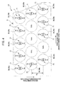
- the plurality of light-emitting element groups 71 are separated from each other and arranged in a matrix of three rows by n columns (n is an integer of two or more) so as to correspond to the plurality of lenses 64 described above (for example, see Fig. 4 ).
- Each of the light-emitting element groups 71 is configured to include a plurality (8 in the present embodiment) of light-emitting elements 74.
- the eight light-emitting elements 74 that constitute each of the light-emitting element groups 71 are arranged along a lower surface 721 of the supporting plate 72 illustrated in Fig. 3 .
- the light L emitted from each of the eight light-emitting elements 74 is focused (imaged) on the light receiving surface 111 of the photosensitive drum 11 through the corresponding lens 64.
- the eight light-emitting elements 74 are separated from each other and are arranged in four columns in the main-scanning direction and in two rows in the sub-scanning direction.
- the eight light-emitting elements 74 are arranged in a matrix of two rows by four columns.
- the two adjacent light-emitting elements 74 belonging to one column are arranged so as to be offset from each other in the main-scanning direction.
- the eight light-emitting elements 74 belonging to one light-emitting element group 71 are arranged in a matrix of two rows by four columns in the present embodiment, the arrangement shape is not limited thereto.
- the eight light-emitting elements 74 may be arranged in a matrix of four rows by two columns.
- the plurality of light-emitting element groups 71 are arranged in a matrix of three rows by n columns so as to be separated from each other. As illustrated in Fig. 4 , the three light-emitting element groups 71 belonging to one column (column of light-emitting element groups) are arranged so as to be offset from each other by an equal distance in the main-scanning direction (right direction in Fig. 4 ).
- the gaps between adjacent light-emitting element groups 71 are sequentially supplemented by the light-emitting element group 71 of a next row and the light-emitting element group 71 of a subsequent row.
- the light-emitting elements 74 are bottom emission-type organic electroluminescence (EL) element.
- the light-emitting elements 74 are not limited to the bottom emission-type elements and may be top emission-type elements.
- the support portion 72 is not required to have optically transparent properties as described above.
- the gaps (pitches) between the light-emitting elements 74 can be set to be relatively small. In this way, the recording density of the recording medium P when an image is recorded on the recording medium P can be made relatively high.
- the light-emitting elements 74 can be formed with highly accurate sizes and at highly accurate positions by using various film-forming methods. As a result, it is possible to obtain the recording medium P carrying thereon a clearer image.
- all of the light-emitting elements 74 are configured to emit red light.
- the constituent materials of a light-emitting layer which emits red light (4-dicyanomethylene)-2-methyl-6-paradimethylaminostyryl)-4H-pyrane (DCM), Nile Red and the like can be mentioned.
- the light-emitting elements 74 are not limited to those configured to emit red light, but may be configured to emit monochromatic light of another color or white light.
- the light L emitted from the light-emitting layer can be appropriately set to monochromatic light of an arbitrary color in accordance with the constituent materials of the light-emitting layer.
- the spectral sensitivity characteristic of the photosensitive drum used in the electrophotographic process is generally set to have a peak in a wavelength range of a red wavelength, which is the emission wavelength of a semiconductor laser, to a near-red wavelength, it is preferable to use the materials capable of emitting red light as described above.
- the light shielding member 82, the diaphragm member 83, and the light shielding member 81 are provided between the lens array 6 and the light-emitting element array 7.
- the light shielding members 81 and 82 are configured to prevent crosstalk of the light L between the adjacent light-emitting element groups 71.
- a plurality of through-holes (openings) 811 is formed in the light shielding member 81 so as to pass through the light shielding member 81 in the up and down direction (thickness direction) of Fig. 3 .
- These through-holes 811 are arranged at positions corresponding to the respective lenses 64.
- a plurality of through-holes 821 is formed in the light shielding member 82 so as to pass through the light shielding member 82 in the up and down direction (thickness direction) of Fig. 3 .
- These through-holes 821 are arranged at positions corresponding to the respective lenses 64.
- Each of the through-holes 811 and 821 is configured to form an optical path which extends from the light-emitting element group 71 to the corresponding lens 64.
- each of the through-holes 811 and 821 has a circular shape in plan view thereof and includes therein the eight light-emitting elements 74 of the light-emitting element group 71 corresponding to each of the through-holes 811 and 821.
- the through-holes 811 and 821 have a cylindrical shape in the configuration illustrated in Fig. 3 , the invention is not limited thereto.
- the through-holes 811 and 821 may have a circular truncated cone shape which expands upward.
- the diaphragm member 83 is provided between the light shielding members 81 and 82.
- the diaphragm member 83 is an aperture diaphragm that restricts the amount of light L incident on the lens 64 from the light-emitting element group 71 to a predetermined amount.
- the diaphragm member 83 is disposed in the vicinity of a front-side focal plane of the optical system 60. Therefore, the optical system 60 becomes telecentric on the image side. Even when there is an error in the distance between the light receiving surface 111 and the line head 13 due to mounting errors or the like, it is possible to prevent the deviation of an imaging position in each of the light-emitting elements 74a, 74d, 74b, and 74c (first and second light-emitting elements).
- the diaphragm member 83 has a planar or layered shape, and a plurality of through-hole (openings) 831 is formed in the diaphragm member 83 so as to pass through the diaphragm member 83 in the up and down direction (thickness dimension) of Fig. 3 .
- These through-holes 831 are arranged at positions corresponding to the lenses 64 (namely, the above-described through-holes 811 and 821).
- each of the through-holes 831 of the diaphragm member 83 has a circular shape in plan view thereof and has a diameter smaller than that of the through-holes 811 of the light shielding member 81 described above.
- the diaphragm member 83 is preferably configured to set a distance to the lens 64 so as to be relatively small. By doing so, light emitted from light-emitting elements 74 which are located at different distances from the optical axis 601 (that is, even when the light-emitting elements 74 are located at different angles of view) can be made incident to approximately the same region of the lens 64.
- the light shielding members 81 and 82 and the diaphragm member 83 also have a function of regulating the distance, positional relationship, and attitude between the lens array 6 and the support portion 72 with high accuracy.
- the distance between the lens surface 62 of each lens 64 and the corresponding light-emitting element group 71 is an important condition (element) that determines the position in the up and down direction of Fig. 3 of the imaging position of the optical system 60 which will be described later. Therefore, as described above, when the light shielding members 81 and 82 and the diaphragm member 83 functions as the spacer that regulates the gap length which is the distance between the lens array 6 and the light-emitting element array 7, it is possible to obtain the image forming apparatus 1 which is highly precise and reliable.
- the light shielding member 81 and 82 and the diaphragm member 83 preferably have at least the inner peripheral surface thereof which has a dark color such as black, brown, or dark blue.
- constituent materials of the light shielding members 81 and 82 and the diaphragm member 83 are not particularly limited as long as they are not optically transparent, various kinds of coloring agents, metallic materials such as chrome or chromic oxides, resins having mixed therein carbon black or coloring agents, and the like can be mentioned as example thereof.
- the casing 9 has a frame member (casing body) 91, a lid member (bottom lid) 92, and a plurality of clamp members 93 which fixedly secures the frame member 91 to the lid member 92 (see Fig. 3 ).
- the frame member 91 has a generally long shape, as illustrated in Figs. 2 , 5 , and 6 .
- the frame member 91 has a frame shape, and an inner cavity portion 911 that is open to the upper and lower sides of the frame member 91 is formed in the frame member 91 as illustrated in Fig. 3 .
- the width of the inner cavity portion 911 gradually decreases upwardly from the lower side of Fig. 3 .
- the lens array 6', the spacer 84, the lens array 6, the light shielding member 82, the diaphragm member 83, the light shielding member 81, and the light-emitting element array 7 are inserted in the inner cavity portion 911, and they are fixed by adhesive, for example.
- the lens array 6', the spacer 84, the lens array 6, the light shielding member 82, the diaphragm member 83, the light shielding member 81, and the light-emitting element array 7 are collectively held on the frame member 91, such that the positions in the main and sub-scanning directions of the lens array 6', the spacer 84, the lens array 6, the light shielding member 82, the diaphragm member 83, the light shielding member 81, and the light-emitting element array 7 are determined.
- an upper surface 722 of the supporting plate 72 of the light-emitting element array 7 is in contact (abutting contact) with a stepped portion 915, which is formed on a wall surface of the inner cavity portion 911, and the lower surface of the second light shielding member 81.
- the lid member 92 is inserted into the inner cavity portion 911 from the lower side.
- the lid member 92 is formed of a lengthy member having a recess portion 922 in which the accommodation portion 73 is inserted at an upper side thereof.
- the edge portions of the support portion 72 of the light-emitting element array 7 are pinched between the upper end surface of the lid member 92 and the boundary portion 915 of the frame member 91.
- the lid member 92 is pressed upward by each of the clamp members 93. In this way, the lid member 92 is fixed to the frame member 91. In addition, by the pressed lid member 92, the positional relationships among the light-emitting element array 7, the light shielding members 81 and 82, the diaphragm member 83, and the lens array 6 in the main-scanning direction, the sub-scanning direction, and the up and down direction of Fig. 3 are fixed.
- the clamp members 93 are preferably arranged in plural numbers at equal intervals in the main-scanning direction. Accordingly, the frame member 91 and the lid member 92 can be pinched uniformly in the main-scanning direction.
- the clamp member 93 has a generally U shape in the cross section illustrated in Fig. 3 and is formed by folding a metallic plate. Both ends of the clamp member 93 are bent inward to form claws portions 931. The claw portions 931 are engaged with shoulder portions 916 of the frame member 91.
- a curved portion 932 which is curved upward in an arch shape is formed in the middle portion of the clamp member 93.
- the apex of the curved portion 932 is in pressure-contact with the lower surface of the lid member 92 in a state where the claw portions 931 are engaged with the shoulder portion 916. In this way, the curved portion 932 urges the lid member 92 upwardly in a state where the curved portion 932 is elastically deformed.
- the lid member 92 can be detached from the frame member 91. Then, it is possible to perform maintenance, such as replacement and repair, for the light-emitting element array 7.
- the constituent materials of the frame member 91 and the lid member 92 are not particularly limited, and the same constituent materials as the supporting plate 72 may be used, for example.
- the constituent materials of the clamp member 93 are not particularly limited, and aluminum or stainless steel may be used, for example.
- the clamp member 93 may also be formed of a hard resin material.
- the frame member 91 has spacers which are provided at both ends in the longitudinal direction thereof so as to protrude upward.
- the spacers are configured to regulate the distance between the light receiving surface 111 and the lens array 6.
- a pair of lenses 64 and 64' corresponding to the light-emitting element group 71 are arranged in the optical axis direction (namely, the lenses 64 and 64' are arranged in the symmetrical axis direction of the lens 64). As illustrated in Fig. 5 , this pair of lenses 64 and 64' constitutes the optical system 60 that images the light L from the light-emitting elements 74 belonging to the corresponding light-emitting element group 71.
- a cross section which contains the optical axis 601 and is in parallel to the main-scanning direction
- a cross section which contains the optical axis 601 and is perpendicular to the main-cross section
- a cross section which contains the optical axis 601 and is perpendicular to the main-cross section
- Fig. 5 illustrates a view of the optical system 60 taken along the main-cross section.
- the optical system 60 formed by a pair of lenses 64a and 64a' will be referred to as an "optical system 60a”
- the optical system 60 formed by a pair of lenses 64b and 64b' will be referred to as an "optical system 60b”
- the optical system 60 formed by a pair of lenses 64c and 64c' will be referred to as an "optical system 60c”.
- the light-emitting elements 74a, 74b, 74c, and 74d are disposed at different positions in the main-scanning direction (first direction), and arbitrary two light-emitting elements of these light-emitting elements 74a, 74b, 74c, and 74d constitute first or second light-emitting elements.
- the optical system 60 is configured to image the light L having passed through the through-holes (aperture diaphragm) 831 of the diaphragm member 83 in the vicinity of the light receiving surface 111 of the photoconductor 11.
- the optical system 60 is plane-symmetrical (mirror-symmetrical) with respect to a symmetry plane (first symmetry plane) perpendicular in the main-scanning direction (first direction), and the optical system 60 is plane-symmetrical (mirror-symmetrical) with respect to a symmetry plane (second symmetry plane) perpendicular in the sub-scanning direction (second direction).
- first symmetry plane a symmetry plane
- second symmetry plane perpendicular in the sub-scanning direction
- An intersecting line of these two symmetry planes will be referred to as the axis of symmetry.
- the axis of symmetry is identical to the optical axis.
- the optical axis of the optical system 60 is not defined. In the following description, the above-described axis of symmetry will be described as the optical axis for the convenience sake.
- Fig. 5 in the optical system 60, when light is incident from the side of the light-emitting element 74, the light is imaged at different positions (imaging points FP0, FP1, and FP2) depending on the portion of the optical system 60 through which the light passes.
- the rays of light are illustrated, assuming that light emitted from an intersecting point (hereinafter referred to as a "virtual light source") of the lower surface 721 of the support portion 72 and the optical axis 601 is incident to the optical system 60.
- the imaging point FP0 is a position (paraxial imaging point) at which, when the light emitted from the virtual light source is incident in the vicinity of the optical axis 601 of the optical system 60, the ray of the light (the emitted light) intersects the optical axis 601.
- the imaging point FP1 is the position closest to the optical system 60 among the positions at which, when the light emitted from the virtual light source is incident to the optical system 60 via the diaphragm member 83, the ray of the light (the emitted light) intersects the optical axis 601.
- the imaging point FP2 is the position farthest from the optical system 60 among the positions at which, when the light emitted from the virtual light source is incident to the optical system 60 via the diaphragm member 83, the ray of the light (the emitted light) intersects the optical axis 601.
- the optical system 60 has a longitudinal aberration on the side of the optical system 60 and the opposite side with respect to the imaging point FP0. That is to say, the optical system 60 has a longitudinal aberration of which the signs are reversed with respect to an image surface 1.
- the distance between the imaging points FP1 and FP2 corresponds to the difference between the maximum value and the minimum value of the longitudinal aberration.
- the spot size of the light L from the light-emitting element 74 can be made to be small and substantially constant for the ray of light imaged at a imaging point located between the imaging point FP1 and the imaging point FP2 which are respectively located closet and furthest from the optical system 60, among the plurality of imaging points FP0, FP1, and FP2.
- the optical magnification ⁇ of the optical system 60 satisfies the relation of
- the light-emitting element group 71 includes the eight light-emitting elements 74 which are arranged in a matrix of two rows by four columns, and the distance P el is the distance between the centers of two adjacent light-emitting elements 74 as seen from the main-cross section.
- the centers of the light-emitting elements are the centers of geometry of the light-emitting elements, and the distance P el is the distance in the main-scanning direction between the centers of geometry of the light-emitting elements.
- the light emitted from the two adjacent light-emitting elements 74 as seen from the main-cross section forms two adjacent pixels on the light receiving surface 111. Therefore,
- the optical system 60 has the front-side focal plane FP0 in the vicinity of the optical axis 601 so as to be located between the imaging point FP1 and the imaging point FP2, it is possible to increase the distance between the imaging point FP1 and the imaging point FP2 (namely, the difference G between the maximum value and the minimum value of the longitudinal aberration) while satisfying other optical characteristics needed by the optical system 60.
- the distance between the imaging point FP1 and the imaging point FP2 namely, the difference G between the maximum value and the minimum value of the longitudinal aberration
- the optical system 60 is preferably configured such that the distance in the optical axis direction between the imaging point FP2 and the imaging point FP1, which are respectively located furthest and closet from the optical system 60 (namely, the difference G between the maximum value and the minimum value of the longitudinal aberration on the main-cross section of the optical system 60), is larger that the spot size of the light emitted from the light-emitting element 74 (namely, the spot size on the image surface I).
- the optical system 60 having such characteristics can be realized by a multifocal lens having different focal points.
- the lenses 64 are configured as multifocal lenses having a plurality of focal points, and the lenses 64' are configured as single focus lenses having a single focal point so that the optical system 60 is configured to have the plurality of above-described imaging points FP1, FP1, and FP2.
- the lens 64 is formed on the support portion 65 which is formed of a glass material, for example.
- the lens 64 has a lens surface 62 on an opposite side to the support portion 65.
- the lens surface 62 of the lens 64 is formed so that the lens 64 has a plurality of focal points fp0, fp1, and fp2 which are located at different positions in the optical axis direction.
- the focal point fp0 is a position (paraxial focal point) at which, when light parallel to the optical axis 601 (namely, light from infinite distance) is incident in the vicinity of the optical axis 601 of the lens 64, the ray of the light (the emitted light) intersects the optical axis 601.
- the focal point fp1 is the position closest to the lens 64 among the positions at which, when light parallel to the optical axis 601 is incident to the lens 64 via the diaphragm member 83, the ray of the light (the emitted light) intersects the optical axis 601.
- the focal point fp2 is the position farthest from the lens 64 among the positions at which, when light parallel to the optical axis 601 is incident to the lens 64 via the diaphragm member 83, the ray of the light (the emitted light) intersects the optical axis 601.
- the lens 64 has a longitudinal aberration on the side of the lens 64 and the opposite side with respect to the focal point fp0.
- the difference between the maximum value and the minimum value of the longitudinal aberration corresponds to the distance g between the focal points fp1 and fp2.
- the lens surface 62 of the lens 64 has a first circular region 62a which is defined at a central portion thereof (so as to include the intersection with the axis of symmetry of the lens 64) and a second ringshaped region 62b which is defined around the first region 62a.
- a region, through which the light having passed through the diaphragm member (aperture diaphragm) 83 passes, is indicated by broken lines.
- the surface shape of the first region 62a and the surface shape of the second region 69b are defined by different definition formulas.
- a definition formula (rotationally symmetrical aspheric surface) expressed by Formula 1 below can be used, for example (see Examples below for more details). In this way, the lens 64 having the above-described characteristics can be realized relatively easily and reliably.
- the respective coefficients A to C and A of the definition formula are appropriately set in accordance with the focal distance of the optical system 60, the shape of the lens surface 62' of the lens 64', and the like so that the optical system 60 has a plurality of above-described imaging points.
- the first region 62a and the second region 62b will be expressed by different definition formulas.
- optical axis in the definition formula refers to the axis of symmetry of a rotationally symmetrical lens.
- the size of the first region 62a is larger than the size of the second region 62b. By doing so, the size of the first region 62a within the light passing region a can be made to be substantially the same as the size of the second region 62b within the light passing region a. As a result, even when the positions in the optical axis direction of the image surface and the light receiving surface 111 are changed, light amount unevenness (concentration unevenness) of the spots formed on the light receiving surface 111 can be suppressed.
- the optical system 60 has a plurality of lenses 64 and 64' which are arranged in the optical axis direction thereof.
- an aperture diaphragm-side lens surface of the lens 64 disposed closest to the aperture diaphragm 83 is configured as the above-described lens surface 62 having the first region 62a and the second region 62b. Therefore, light emitted from light-emitting elements 74 which are located at different distances from the optical axis 601 (that is, even when the light-emitting elements 74 provide different angles of view) can be prevented from being offset in the light passing region on the lens surface 62. Accordingly, the above-described advantage of increasing the focal depth of the optical system 60 can be obtained by the other light-emitting elements 74.
- the lens surface 62 including the first region 62a and the second region 62b is provided on the side of the lens 64 close to the light-emitting elements 74, it is possible to suppress characteristic variation due to an angle of view.
- the lens 64' is formed on a support portion 65' which is formed of a glass material, for example.
- the lens 64' has a lens surface 62' on an opposite side to the support portion 65'.
- the lens surface 62' of the lens 64' may be a spherical surface or an aspheric surface, and a surface shape thereof can be defined by one definition formula.
- a definition formula (xy polynomial surface) expressed by Formula 2 below can be used, for example (see Examples below for more details).
- the respective coefficients A to I of the definition formula are appropriately set in accordance with the focal distance of the optical system 60, the shape of the lens surface 62 of the lens 64, and the like so that the optical system 60 has a plurality of above-described imaging points.
- the optical system 60 is configured such that the second region 62b is provided closer to the outer periphery of the lens surface 62 than the first region 62a and is in contact with the first region 62a.
- the minimum value of a longitudinal aberration of light passing through the first region 62a namely, the longitudinal aberration of light having passed through the vicinity of a boundary thereof
- the maximum value of a longitudinal aberration of light having passed through the second region 62b namely, the longitudinal aberration of light having passed through the vicinity of a boundary thereof
- the longitudinal aberration ⁇ 1 is negative, and the longitudinal aberration ⁇ 2 is positive. Therefore, the difference between the longitudinal aberration ⁇ 1 and the longitudinal aberration ⁇ 2 can be effectively increased. Furthermore, the difference G between the maximum value and the minimum value of the longitudinal aberration can be effectively increased.
- the first region 62a is provided so as to include the center of the lens surface 62.
- a lens 64A may be used which has a lens surface 62A configured by three regions 62c, 62d, and 62e having different definition formulas, in lieu of the lens surface 62.
- the region (third region) 62c is provided so as to include the intersection with the axis of symmetry of the lens 64A.
- the region (first region) 62d is provided closer to the outer periphery of the lens surface 62A than the region 62c and is in contact with the region 62c.
- the region 62e is provided closer to the outer periphery of the lens surface 62A than the region 62d and is in contact with the region 62d.
- the lens surface 62A illustrated in Figs. 11A and 11B includes the region (third region) 62c which is provided closer to the inner periphery of the lens surface 62A than the region (first region) 62d so as to include the center of the lens surface 62A and be in contact with the region 62d and which has a surface shape that is defined by a definition formula different from that of the region 62d.
- a longitudinal aberration of light having passed through the region 62d in the vicinity of its boundary with the region 62e is defined as ⁇ 1
- a longitudinal aberration of light having passed through the region 62e in the vicinity of its boundary with the region 62d is defined as ⁇ 2
- the respective rays of light L1, L2, L3, and L4 are imaged (focused) in the vicinity of the light receiving surface 111 of the photoconductor 11 as illustrated in Fig. 10 .
- the light L1 is imaged at a plurality of imaging positions IFP10, IFP11, and IFP12 which are located at different positions in its travelling direction (third direction).
- the imaging position IFP10 is a position (paraxial imaging point) at which, when the light L1 emitted from the light-emitting element 74a is incident to the lens 64 via the diaphragm member 83, the ray of light passing through the vicinity of the optical axis 601 is imaged (focused).
- the imaging position IFP11 is the position closet to the optical system 60 among the positions at which, when the light L1 emitted from the light-emitting element 74a is incident to the lens 64 via the diaphragm member 83, the ray of light passing through the first region 62a of the lens 64 is imaged (focused).
- the imaging position IFP12 is the position furthest from the optical system 60 among the positions at which, when the light L1 emitted from the light-emitting element 74a is incident to the lens 64 via the diaphragm member 83, the ray of light passing through the second region 62b of the lens 64 is imaged (focused).
- the light L2 is imaged at a plurality of imaging positions IFP20, IFP21, and IFP22 which are located at different positions in its travelling direction (third direction).
- the light L3 is imaged at a plurality of imaging positions IFP30, IFP31, and IFP32 which are located at different positions in its travelling direction (third direction).
- the light L4 is imaged at a plurality of imaging positions IFP40, IFP41, and IFP42 which are located at different positions in its travelling direction (third direction).
- the respective rays of light L1, L2, L3, and L4 imaged by the optical system 60 will have their spot sizes which are substantially constant over a relatively wide range (distance G1) in the optical axis direction in the vicinity of the image surface.
- the optical system 60 is configured so that the respective imaging positions IFP10, IFP20, IFP30, and IFP40 are located in the vicinity of the light receiving surface 111.
- the light receiving surface 111 is positioned between the imaging positions IFP11 and IFP12, between the imaging positions IFP21 and IFP22, between the imaging positions IFP31 and IFP32, and between the imaging positions IFP41 and IFP42.
- Fig. 10 illustrates a case where the optical system 60 has an image-surface curvature.
- the imaging position IFP10 of the light L1 the imaging position IFP20 of the light L2, the imaging position IFP30 of the light L3, and the imaging position IFP40 of the light L4 are located on a curved image surface I. Therefore, the imaging positions IFP 10 and IFP40 and the imaging positions IFP20 and IFP30 are offset from each other in the optical axis direction.
- two light-emitting elements 74b and 74c are located at positions close to the optical axis 601 of the optical system 60, and the other two light-emitting elements 74a and 74d are located at positions distant from the optical axis 601.
- the light-emitting elements 74a and 74d and the light-emitting elements 74b and 74c have different angles of view.
- the imaging positions IFP10 and IFP40 and the imaging positions IFP20 and IFP30 are sometimes offset in the optical axis direction (third direction) due to the image-surface curvature of the optical system 60.
- the above-described distance between the imaging point FP1 and the imaging point FP2 (namely, the difference G between the maximum value and the minimum value of the longitudinal aberration) is larger than the maximum value G1 of the offset amount. Therefore, even when the image surface I of the optical system 60 and the light receiving surface 111 are slightly offset in the optical axis direction, it is possible to decrease the difference on the light receiving surface 111 between the spot size of the light from the light-emitting element 74 which is positioned closer to the optical axis 601 and the spot size of the light from the light-emitting element 74 which is positioned distant from the optical axis 601.
- the invention is not limited thereto.
- Each of the components provided in the line head and the image forming apparatus can be replaced with a component having an arbitrary configuration capable of realizing the same function.
- an arbitrary structure may be added.
- a plurality of lenses is not limited to being arranged in a matrix of two rows by n columns.
- a plurality of lenses in each of the lens arrays may be arranged in a matrix of three rows by n columns, four rows by n columns, and the like.
- one optical system may be configured by a plurality of lenses, and may be configured to have one or three or more lens surfaces.
- the light-emitting elements are described as being arranged in a matrix of one row by n columns for the convenience of explanation, the arrangement is not limited to this, and the light-emitting elements may be arranged in a matrix of two rows by n columns, three rows by n columns, and the like.
- FIG. 12 is a cross-sectional view taken along the main-cross section, illustrating the optical system included in the line head according to Example of the invention.
- the line head of the present example had the same configuration as the line head illustrated in Figs. 3 and 5 , except that three light-emitting elements 74 were arranged in the main-scanning direction.
- the three light-emitting elements 74 arranged in the main-scanning direction were arranged symmetrically to the optical axis.
- a glass material was used as the constituent materials of the support portions 65 and 65', and a resin material was used as the constituent materials of the lenses 64 and 64'.
- Table 1 Surface number Curvature at the center of main-cross section Surface spacing Refractive index at reference wavelength
- a surface S1 is a boundary surface (light source plane) of the light-emitting element 74 and the support portion 72
- a surface S2 is a surface (emission surface of a glass substrate) of the support portion 72 opposite to the light-emitting element 74
- a surface S3 is a surface (aperture diaphragm) of the diaphragm member 83 close to the light-emitting element 74
- a surface S4 is the lens surface 62 (incidence surface of a resin portion) of the lens 64
- a surface S5 is a boundary surface (resin-glass boundary surface) of the lens 64 and the support portion 65
- a surface S6 is a surface (emission surface of the glass substrate) of the support portion 65 opposite to the lens 64
- a surface S7 is the lens surface 62' (incidence surface of the resin portion) of the lens 64'
- a surface S8 is a boundary portion (resin-glass boundary surface) of the lens
- a surface spacing d1 is a spacing between the surface S1 and the surface S2
- a surface spacing d2 is a spacing between the surface S2 and the surface S3
- a surface spacing d3 is a spacing between the surface S3 and the surface S4
- a surface spacing d4 is a spacing between the surface S4 and the surface S5
- a surface spacing d5 is a spacing between the surface S5 and the surface S6
- a surface spacing d6 is a spacing between the surface S6 and the surface S7
- a surface spacing d7 is a spacing between the surface S7 and the surface S8
- a surface spacing d9 is a spacing between the surface S9 and the surface S10.
- a refractive index at reference wavelength is the refractive indexes on the respective surfaces with light having the reference wavelength.
- the wavelength (reference wavelength) of the light emitted from the light-emitting element 74 was 690 nm, the object-side numerical aperture was 0.153, the total width of the object-side pixel group in the main-scanning direction was 1.176 mm, and the total width of the object-side pixel group in the sub-scanning direction was 0.127 mm.
- the distance (pitch) P el between adjacent light-emitting elements in the main-scanning direction was 0.042 mm
- the optical magnification ⁇ of the optical system was -0.5039.
- the lens surface 62 of the lens 64 was configured such that a range of regions within a radius of 0 to 0.604 mm around the optical axis was defined as the first region, and a range of regions outside the radius 0.604 mm around the optical axis was defined as the second region.
- the surface shapes of the respective regions were defined using the coefficients shown below in the definition formula given by Formula 1.
- the surface shape of the lens surface 62' of the lens 64' was defined using the coefficients shown below in the definition formula given by Formula 2.
- the optical system obtained in the above-described manner had a longitudinal aberration as shown in Fig. 13 .
- the horizontal axis is defined such that, when the 0 (reference) point of the horizontal axis corresponds to a longitudinal aberration in the vicinity of the optical axis, the left side is the light source side and the right side is the image side.
- the vertical axis represents the separation distance of the ray of light having passed through the diaphragm member 83 from the optical axis when the center of the diaphragm member (aperture diaphragm) 83 is at 0, and the radius of the through-hole (opening) of the diaphragm member 83 is set to 1.
- a line head was designed similar to the above-described example, except that the surface shape of the lens surface 62 of the lens 64 was made identical to the surface shape of the lens surface 62' of the lens 64', and the characteristics thereof were evaluated by simulation.
- Figs. 14A and 14B respectively illustrate changes in the spot sizes at various positions in the optical axis direction of the optical systems of the example and the comparative example.
- Fig. 14A is for the example of the invention, and Fig. 14B is for the comparative example.
- the line head (optical system) of the example according to the invention was better able to suppress a change in the spot size in the vicinity of the minimum spot size than the line head of the comparative example.
- the line head of the example was mounted on the image forming apparatus as shown in Fig. 1 , it was possible to obtain high-quality images in which concentration unevenness was suppressed.
Landscapes
- Physics & Mathematics (AREA)
- General Physics & Mathematics (AREA)
- Optics & Photonics (AREA)
- Printers Or Recording Devices Using Electromagnetic And Radiation Means (AREA)
- Facsimile Heads (AREA)
- Lenses (AREA)
Abstract
An image forming apparatus includes a latent image carrier on which a latent image is formed; and a line head that performs exposure on the latent image carrier so as to form the latent image, the line head including: a first light-emitting element and a second light-emitting element that are arranged in a first direction; and an optical system that images light emitted from the first light-emitting element and the second light-emitting element, in which when a difference between the maximum value and the minimum value of a longitudinal aberration of the optical system is defined as G, a distance in the first direction between a center of geometry of the first light-emitting element and a center of geometry of the second light-emitting element is defined as Pel, and an optical magnification of the optical system is defined as β, a relation of G>|β|·Pel is satisfied.
Description
- The present invention relates to a line head and an image forming apparatus.
- Electrophotographic image forming apparatuses such as copying machines or printers are provided with an exposure unit that performs an exposure process on an outer surface of a rotating photoconductor so as to form an electrostatic latent image thereon.
As the exposure unit, a line head having a structure in which a plurality of light-emitting elements is arranged in the direction of the rotation axis of the photoconductor is known (for example, seeJP-A-2-4546 - As the line head, for example,
JP-A-2-4546 - In the optical information writer, the plurality of LEDs of each of the LED array chips is arranged in the direction of the rotation axis of the photoconductor. Convex lens elements (optical systems) are provided so as to correspond to the respective LED array chips. The convex lens elements image the rays of light from the respective LEDs of each of the LED array chip.
- In the line head described in
JP-A-2-4546 - Furthermore, since the positional relationship between the image surface of the convex lens element and the light irradiation surface (the surface of the photoconductor) is offset or varied due to errors in mounting the line head onto the body of the image forming apparatus, eccentricity of the photoconductor, or the like, the spot size will vary. In this respect, the obtained images will have concentration unevenness.
- An advantage of some aspects of the invention is that it provides a line head capable of performing a high-accuracy exposure process and an image forming apparatus capable of obtaining a high-quality image.
- The above-described advantage is achieved by the following aspects and embodiments of the invention.
- According to an aspect of the invention, there is provided a line head including: a first light-emitting element and a second light-emitting element that are arranged in a first direction; and an optical system that images light emitted from the first light-emitting element and the second light-emitting element, wherein when a difference between the maximum value and the minimum value of a longitudinal aberration of the optical system is defined as G, a distance in the first direction between a center of geometry of the first light-emitting element and a center of geometry of the second light-emitting element is defined as Pel, and an optical magnification of the optical system is defined as β, a relation of G>|β|·Pel is satisfied.
- In an embodiment of the line head of the above aspect of the invention, the optical system may have a lens surface that includes a first region and second region, of which the surface shapes are defined by different definition formulas. The second region may be arranged so as to surround the first region in a ring shape. When a imaging point on an optical axis is used as a reference, and a light travelling direction of the optical axis is defined as a positive direction, the optical system may be configured such that when, among the light emitted from the first light-emitting element, the minimum value of a longitudinal aberration of light passing through the first region is defined as Δ1, and the maximum value of light passing through the second region is defined as Δ2, a relation of Δ2-Δ1=G is satisfied.
- In another embodiment of the line head of the above aspect of the invention, three or more light-emitting elements including the first light-emitting element and the second light-emitting element may be arranged in the first direction. Among the three light-emitting elements, the first light-emitting element and the second light-emitting element may be adjacent to each other in the first direction.
- In another embodiment of the line head of the above aspect of the invention, the lens surface may include a third region which is defined by a definition formula different from that of the first region and is provided so as to include an intersection with the optical axis. The first region may be arranged so as to surround the third region in a ring shape.
- In another embodiment of the line head of the above aspect of the invention, the minimum value Δ1 of the longitudinal aberration of light passing through the first region may have a negative sign, and the maximum value of the longitudinal aberration Δ2 of light passing through the second region may have a positive sign.
- In another embodiment of the line head of the above aspect of the invention, an aperture diaphragm may be provided close to a front-side focal point of the optical system.
- In another embodiment of the line head of the above aspect of the invention, the first region and the second region may be included in a lens surface which is located closest to the aperture diaphragm among the lens surfaces of the optical system.
- According to an aspect of the invention, there is provided an image forming apparatus including: a latent image carrier on which a latent image is formed; and a line head that performs exposure on the latent image carrier so as to form the latent image, the line head including: a first light-emitting element and a second light-emitting element that are arranged in a first direction; and an optical system that images light emitted from the first light-emitting element and the second light-emitting element, in which when a difference between the maximum value and the minimum value of a longitudinal aberration of the optical system is defined as G, a distance in the first direction between a center of geometry of the first light-emitting element and a center of geometry of the second light-emitting element is defined as Pel, and an optical magnification of the optical system is defined as β, a relation of G>|β|·Pel is satisfied.
- According to the line head of the aspects and embodiments of the invention having the above-described configuration, when the light emitted from the light-emitting element is imaged by the optical system, it is possible to make the spot size of the light substantially constant over a relatively wide range in the optical axis direction in the vicinity of the image surface (that is to say, it is possible to increase the focal depth). Therefore, even when the positional relationship in the optical axis direction between the image surface and the light irradiation surface, is changed or offset, it is possible to prevent a variation of the spot size on the light irradiation surface. As a result, it is possible to realize a high-accuracy exposure process.
- Moreover, according to the image forming apparatus of the aspect of the invention, by realizing the above-described high-accuracy exposure process, it is possible to obtain a high-quality image in which concentration unevenness is suppressed.
- The invention will be described with reference to the accompanying drawings, wherein like numbers reference like elements.
-
Fig. 1 is a schematic view illustrating the entire configuration of an image forming apparatus according to an embodiment of the invention. -
Fig. 2 is a partially sectional perspective view illustrating a line head included in the image forming apparatus illustrated inFig. 1 . -
Fig. 3 is a cross-sectional view taken along the line III-III ofFig. 2 . -
Fig. 4 is a plan view of the line head illustrated inFig. 2 , illustrating the positional relationship between lenses and light-emitting elements. -
Fig. 5 is a cross-sectional view, taken along the main-scanning direction, of an optical system included in the line head illustrated inFig. 2 . -
Fig. 6 is a cross-sectional view, taken along the main-scanning direction, for describing an optical magnification of the optical system included in the line head illustrated inFig. 2 . -
Fig. 7 is a plan view illustrating another example of the arrangement of light-emitting elements. -
Figs. 8A and 8B are views illustrating a light-emitting element-side lens included in the optical system illustrated inFig. 5 . -
Fig. 9 is a view for describing the operation of the lens illustrated inFigs. 8A and 8B . -
Fig. 10 is a view for describing the operation of the optical system illustrated inFig. 5 . -
Figs. 11A and 11B are views illustrating another example of the light-emitting element-side lens included in the optical system illustrated inFig. 5 . -
Fig. 12 is a view illustrating an optical system included in a line head according to Example of the invention. -
Fig. 13 is a graph illustrating the longitudinal aberration of an optical system included in a line head according to Example of the invention. -
Figs. 14A and 14B are graphs illustrating the spot sizes in the vicinity of a photoconductor surface (an image surface), respectively, of the optical system of the line head of Example of the invention and the optical system of the line head of Comparative Example. - Hereinafter, a line head and an image forming apparatus according to preferred embodiments of the invention will be described in detail with reference to the accompanying drawings.
-
Fig. 1 is a schematic view illustrating the entire configuration of an image forming apparatus according to an embodiment of the invention.Fig. 2 is a partially sectional perspective view illustrating a line head included in the image forming apparatus illustrated inFig. 1 .Fig. 3 is a cross-sectional view taken along the line III-III ofFig. 2 .
Fig. 4 is a plan view of the line head illustrated inFig. 2 , illustrating the positional relationship between lenses and light-emitting elements.Fig. 5 is a cross-sectional view, taken along the first direction, of an optical system included in the line head illustrated inFig. 2 .Fig. 6 is a cross-sectional view, taken along the main-scanning direction, for describing an optical magnification of the optical system included in the line head illustrated inFig. 2 .Fig. 7 is a plan view illustrating another example of the arrangement of light-emitting elements.Figs. 8A and 8B are views illustrating a light-emitting element-side lens included in the optical system illustrated inFig. 5 .Fig. 9 is a view for describing the operation of the lens illustrated inFigs. 8A and 8B .Fig. 10 is a view for describing the operation of the optical system illustrated inFig. 5 .Figs. 11A and 11B are views illustrating another example of the light-emitting element-side lens included in the optical system illustrated inFig. 5 . In the following description, it is assumed that an upper side inFigs. 1 to 3 andFig. 5 is "upper" or "upward" and a lower side in the drawings is "lower" or "downward" for the convenience of explanation. - An
image forming apparatus 1 illustrated inFig. 1 is an electrophotographic printer that records an image on a recording medium P by a series of image forming processes including an electrical charging process, an exposure process, a developing process, a transferring process, and a fixing process. In the present embodiment, theimage forming apparatus 1 is a so-called a tandem type color printer. - As illustrated in
Fig. 1 , theimage forming apparatus 1 includes: animage forming unit 10 for the electrical charging process, the exposure process, the developing process; atransfer unit 20 for the transferring process; a fixingunit 30 for the fixing process; atransport mechanism 40 for transporting the recording mediums P, such as paper; and apaper feed unit 50 that supplies the recording medium P to thetransport mechanism 40. - The
image forming unit 10 has four image forming stations: animage forming station 10Y that forms a yellow toner image, animage forming station 10M that forms a magenta toner image, animage forming station 10C that forms a cyan toner image, and animage forming station 10K that forms a black toner image. - Each of the
image forming stations 10Y, 1OC, 1OM, and 10K has a photosensitive drum (photoconductor) 11 which is an electrostatic latent image carrier that carries an electrostatic latent image thereon. A chargingunit 12, a line head (exposure unit) 13, a developingunit 14, and acleaning unit 15 are provided around the periphery (outer peripheral side) of thephotosensitive drum 11 along a rotating direction thereof. Theimage forming stations - The
photosensitive drum 11 has a cylindrical shape as an overall shape and is configured to be rotatable around an axial line thereof along the direction indicated by the arrow inFig. 1 . A photosensitive layer (not shown) is formed in the vicinity of the outer peripheral surface (cylindrical surface) of thephotosensitive drum 11. The outer peripheral surface of thephotosensitive drum 11 forms alight receiving surface 111 that receives light L (emitted light) from theline head 13. - The charging
unit 12 uniformly charges thelight receiving surface 111 of thephotosensitive drum 11 by corona charging or the like. - The
line head 13 receives image information from a host computer (not shown) such as a personal computer and irradiates the light L towards thelight receiving surface 111 of thephotosensitive drum 11 in response to the image information. When the light L is irradiated to the uniformly chargedlight receiving surface 111 of thephotosensitive drum 11, a latent image (electrostatic latent image) corresponding to an irradiation pattern of the light L is formed on thelight receiving surface 111. The configuration of theline head 13 will be described in detail later. - The developing
unit 14 has a reservoir (not shown) storing toner therein and supplies toner from the reservoir to thelight receiving surface 111 of thephotosensitive drum 11 that carries the electrostatic latent image and applies toner thereon. As a result, the latent image on thephotosensitive drum 11 is visualized (developed) as a toner image. - The
cleaning unit 15 has acleaning blade 151, which is made of rubber and makes abutting contact with thelight receiving surface 111 of thephotosensitive drum 11, and is configured to remove toner, which remains on thephotosensitive drum 11 after a primary transfer to be described later, by scraping the remaining toner with thecleaning blade 151. - The
transfer unit 20 is configured to collectively transfer toner images corresponding to respective colors, which are formed on thephotosensitive drums 11 of theimage forming stations - In each of the
image forming stations light receiving surface 111 of thephotosensitive drum 11 performed by the chargingunit 12, exposure of thelight receiving surface 111 performed by theline head 13, supply of toner to thelight receiving surface 111 performed by the developingunit 14, primary transfer to anintermediate transfer belt 21, caused by pressure between theintermediate transfer belt 21 and aprimary transfer roller 22, which will be described later, and cleaning of thelight receiving surface 111 performed by thecleaning unit 15 are sequentially performed while thephotosensitive drum 11 rotates once. - The
transfer unit 20 has theintermediate transfer belt 21 having an endless belt shape. Theintermediate transfer belt 21 is stretched over the plurality (four in the configuration illustrated inFig. 1 ) ofprimary transfer rollers 22, a drivingroller 23, and a drivenroller 24. Theintermediate transfer belt 21 is driven to rotate in the direction indicated by the arrow illustrated inFig. 1 and at approximately the same speed as a circumferential speed of thephotosensitive drum 11 by rotation of the drivingroller 23. - Each
primary transfer roller 22 is provided opposite the correspondingphotosensitive drum 11 with theintermediate transfer belt 21 interposed therebetween and is configured to transfer (primary transfer) a monochrome toner image on thephotosensitive drum 11 to theintermediate transfer belt 21. At the time of primary transfer, a primary transfer voltage (primary transfer bias), which has an opposite polarity to that of electrically charged toner is applied to theprimary transfer roller 22. - A toner image corresponding to at least one of the colors yellow, magenta, cyan, and black is carried on the
intermediate transfer belt 21. For example, when a full color image is formed, toner images corresponding to the four colors yellow, magenta, cyan, and black are sequentially transferred onto theintermediate transfer belt 21 so as to overlap one another so that a full color toner image is formed as an intermediate transfer image. - In addition, the
transfer unit 20 has asecondary transfer roller 25, which is provided opposite the drivingroller 23 with theintermediate transfer belt 21 interposed therebetween, and acleaning unit 26, which is provided opposite the drivenroller 24 with theintermediate transfer belt 21 interposed therebetween. - The
secondary transfer roller 25 is configured to transfer (secondary transfer) a monochrome or full-color toner image (intermediate transfer image), which is formed on theintermediate transfer belt 21, to the recording medium P such as paper, a film, or cloth, which is supplied from thepaper feed unit 50. At the time of secondary transfer, thesecondary transfer roller 25 is pressed against theintermediate transfer belt 21, and a secondary transfer voltage (secondary transfer bias) is applied to thesecondary transfer roller 25. The drivingroller 23 also functions as a backup roller of thesecondary transfer roller 25 at the time of such secondary transfer. - The
cleaning unit 26 has acleaning blade 261, which is made of rubber and makes abutting contact with a surface of theintermediate transfer belt 21, and is configured to remove toner, which remains on theintermediate transfer belt 21 after the secondary transfer, by scraping the remaining toner with thecleaning blade 261. - The fixing
unit 30 has a fixingroller 301 and apressure roller 302 pressed against the fixingroller 301 and is configured such that the recording medium P passes between the fixingroller 301 and thepressure roller 302. In addition, the fixingroller 301 is provided with a heater which is provided at an inside thereof so as to heat an outer peripheral surface of the fixingroller 301 so that the recording medium P passing between the fixingroller 301 and thepressure roller 302 can be heated and pressed. By the fixingunit 30 having such a configuration, the recording medium P having a secondary-transferred toner image thereon is heated and pressed, such that the toner image is heat-fixed on the recording medium P as a permanent image. - The
transport mechanism 40 has a resistroller pair 41, which transports the recording medium P to a secondary transfer position while calculates the timing of paper feeding to the secondary transfer position between thesecondary transfer roller 25 and theintermediate transfer belt 21 described above, and transport roller pairs 42, 43, and 44 which pinch and transport only the recording medium P, on which the fixing process in the fixingunit 30 has been completed. - When an image is formed on only one surface of the recording medium P, the
transport mechanism 40 pinches and transports the recording medium P, in which one surface thereof has been subjected to the fixing process by the fixingunit 30, using thetransport roller pair 42 and discharged the recording medium P to the outside of theimage forming apparatus 1. When images are formed on both surfaces of the recording medium P, the recording medium P in which one surface thereof has been subjected to the fixing process by the fixingunit 30 is first pinched by thetransport roller pair 42. Then, thetransport roller pair 42 is reversely driven and the transport roller pairs 43 and 44 are driven so as to reverse the recording medium P upside down and transport the recording medium P back to the resistroller pair 41. Then, another image is formed on the other surface of the recording medium P by the same operation as described above. - The
paper feed unit 50 is provided with apaper feed cassette 51, which stores therein the recording medium P which has not been used, and apickup roller 52 that feeds the recording medium P from thepaper feed cassette 51 toward the resistroller pair 41 one at a time. - Next, the
line head 13 will be described in detail. In the following description, the longitudinal direction (first direction) of along lens array 6 will be referred to as a "main-scanning direction" and the width direction (second direction) of thelens array 6 will be referred to as a "sub-scanning direction" for the convenience of explanation. - As illustrated in
Fig, 3 , theline head 13 is arranged below thephotosensitive drum 11 so as to oppose thelight receiving surface 111 of thephotosensitive drum 11. Theline head 13 includes a lens array (first lens array) 6', aspacer 84, the lens array (second lens array) 6, a light shielding member (first light shielding member) 82, a diaphragm member (aperture diaphragm) 83, a light shielding member (second light shielding member) 81, and a light-emittingelement array 7, which are sequentially arranged in that order from the side of thephotosensitive drum 11 and are accommodated in acasing 9. - In the
line head 13, the light L emitted from the light-emittingelement array 7 is collimated by thediaphragm member 83 and sequentially passes through the lens array 6' and thelens array 6 to be irradiated onto thelight receiving surface 111 of thephotosensitive drum 11. - As illustrated in
Fig. 2 , thelens arrays 6 and 6' are formed of a planar member having a long appearance. - As illustrated in
Fig. 3 , a plurality of lens surfaces (convex surfaces) 62 is formed on a lower surface (incidence surface) of thelens array 6 on which the light L is incident. On the other hand, an upper surface (emission surface) of thelens array 6 from which the light L is emitted is configured as a flat surface. - That is to say, the
lens array 6 includes a plurality of plano-convex lenses 64, each of the lenses having a convex surface on a surface on which the light L is incident and a flat surface on a surface from which the light L is emitted. Here, a portion of thelens array 6 excluding therespective lenses 64 constitutes asupport portion 65 that supports each of thelenses 64. - Similarly, on a lower surface (incidence surface) of the lens array 6' on which the light L is incident, a plurality of lens surfaces (convex surfaces) 62' is formed so as to correspond to the plurality of lens surfaces 62 described above. On the other hand, an upper surface (emission surface) of the lens array 6' from which the light L is emitted is configured as a flat surface.
- That is to say, the lens array 6' includes a plurality of plano-convex lenses 64', each of the lenses having a convex surface on a surface on which the light L is incident and a flat surface on a surface from which the light L is emitted. Here, a portion of the lens array 6' excluding the respective lenses 64' constitutes a support portion 65' that supports each of the lenses 64'.
- A plurality of lens pairs 64 and 64' constitutes an
optical system 60 that images light emitted from corresponding light-emittingelements 74 of a light-emitting element group 71 (seeFigs. 5 and6 ). The optical system 60 (particularly, the shapes of the lens surfaces of thelenses 64 and 64') will be described in detail later. - The arrangement of the
lenses 64 will be described. Since the lenses 64' have the same arrangement (in plan view) as thelenses 64, the description thereof will be omitted. - As illustrated in
Fig. 4 , thelenses 64 are arranged in plural columns in the main-scanning direction (first direction), and are arranged in plural rows in the sub-scanning direction (second direction) which is orthogonal to the main-scanning direction and the optical axis direction of thelenses 64. - More specifically, the plurality of
lenses 64 are arranged in a matrix of three rows by n columns (n is an integer of two or more). In the following description, among the threelenses 64 belonging to one column (lens array), thelens 64 positioned in the middle will be referred to as a "lens 64b", thelens 64 positioned at a left side inFig. 3 (upper side inFig. 4 ) will be referred to as a "lens 64a", and thelens 64 positioned at a right side inFig. 3 (lower side inFig. 4 ) will be referred to as a "lens 64c". In the lenses 64' which are paired with thelenses 64, the lens 64' corresponding to thelens 64a will be referred to as a "lens 64a"', the lens 64' corresponding to thelens 64b will be referred to as a "lens 64b"', and the lens 64' corresponding to thelens 64c will be referred to as a "lens 64c"'. - In the present embodiment, the
line head 13 is mounted on theimage forming apparatus 1 so that, among the plural lenses 64 (64a to 64c) belonging to one column, thelens 64b positioned closest to the center in the sub-scanning direction is arranged at the position closed to thelight receiving surface 111 of thephotosensitive drum 11. By doing so, the optical characteristics of the plurality oflenses 64 can be configured easily. - As illustrated in
Figs. 2 and4 , in each lens column, thelenses 64a to 64c are sequentially arranged so as to be offset by an equal distance in the main-scanning direction (right direction inFig. 4 ). That is, in each lens column, a line that connects the centers of thelenses 64a to 64c to one another is inclined at a predetermined angle with respect to the main-scanning direction and the sub-scanning direction. - When seen from the cross section illustrated in
Fig. 3 , the threelenses 64 belonging to one lens column, namely thelenses optical axes 601 of thelenses optical axis 601 of thelens 64b. Moreover, theoptical axes 601 of thelenses 64a to 64c are arranged in parallel to each other. - Although the constituent materials of the
lens arrays 6 and 6' are not particularly limited as long as they exhibit the optical characteristics described above, thelens arrays 6 and 6' are preferably formed of a resin material and/or a glass material, for example. - As the resin material, various kinds of resin materials can be used. Examples thereof include liquid crystal polymers such as polyamides, thermoplastic polyimides and polyamideimide aromatic polyesters; polyolefins such as polyphenylene oxide, polyphenylene sulfide and polyethylene; polyesters such as modified polyolefins, polycarbonate, acrylic (methacrylic) resins, polymethyl methacrylate, polyethylene terephthalate and polybutylene terephthalate; thermoplastic resins such as polyethers, polyether ether ketones, polyetherimide and polyacetal; thermosetting resins such as epoxy resins, phenolic resins, urea resins, melamine resins, unsaturated polyester resins and polyimide resins; photocurable resins; and the like. These can be used individually or in combination of two or more species.
- Among these resin materials, resin materials such as thermosetting resins and photocurable resins are preferred because such materials have a relative low thermal expansion coefficient and are rarely thermally expanded (deformed), modified or deteriorated, in addition to the advantages of a relative high refractive index.
- In addition, as the glass material, various kinds of glass materials, such as soda glass, crystalline glass, quartz glass, lead glass, potassium glass, borosilicate glass, alkali-free glass, and the like may be mentioned. When a later-described
support portion 72 of the light-emittingelement array 7 is formed of a glass material, thelens arrays 6 and 6' is preferably formed of a glass material having approximately the same linear expansion rate as the above glass material. By doing so, the positional misalignment of the respective lenses relative to the light-emitting elements due to temperature variation can be prevented. - When the
lens array 6 is formed by using a combination of the described resin material and glass material, a glass substrate formed of a glass material may be used as thesupport portion 65, for example, as will be described later. In this case, a resin layer formed of a resin material may be formed on one surface of the glass substrate, and thelens surface 62 may be formed on the other surface of the glass substrate opposite the resin layer, thus forming the lens 64 (seeFigs. 5 and6 ). In addition, thelens array 6 may be obtained, for example, by forming a plurality of convex portions, which is formed of a resin material and protrudes in a convex surface shape, on one surface of a flat plate-like member (substrate) which is formed of a glass material. - As illustrated in
Figs. 2 and3 , aspacer 84 is provided between thelens arrays 6 and 6'. Thelens arrays 6 and 6' are bonded together via thespacer 84. - The
spacer 84 has a function of regulating a gap length that is a distance between thelens arrays 6 and 6'. - By adjusting the thickness of the
spacer 84, the separation distance between thelenses 64 and 64' can be adjusted to a desired value. - The
spacer 84 has a frame shape which corresponds to the outer peripheral portions of thelens arrays 6 and 6' and is bonded to these peripheral portions. Thespacer 84 is not limited to a frame-shaped member as long as it has the above-described function. Thespacer 84 may be configured as a pair of members which correspond to one of the opposing sides of the outer peripheral portions of thelens arrays 6 and 6'. Alternatively, thespacer 84 may be configured as a planar member having through-holes formed therein so as to correspond to optical paths, similar tolight shielding members - Although the constituent materials of the
spacer 84 are not particularly limited as long as they exhibit the above-described function, a resin material, a metallic material, a glass material, a ceramics material, and the like can be used, for example. - As illustrated in
Fig. 3 , at a side of thelens array 6 on which the light L is incident, the light-emittingelement array 7 is provided with thelight shielding member 82, adiaphragm member 83, and thelight shielding member 81 interposed therebetween. The light-emittingelement array 7 has a plurality of groups of light-emitting elements (light-emitting element groups) 71 and a supporting plate (head substrate) 72. - The supporting
plate 72 is configured to support each of the light-emittingelement groups 71 and is formed of a planar member having a long appearance. The supportingplate 72 is arranged in parallel to thelens array 6. - In addition, the length of the supporting
plate 72 in the main-scanning direction is larger than that of thelens array 6 in the main-scanning direction. The length of the supportingplate 72 in the sub-scanning direction is also set to be larger than that of thelens array 6 in the sub-scanning direction. - Although the constituent materials of the supporting
plate 72 are not particularly limited, when the light-emittingelement groups 71 are provided on the bottom surface side of the support portion 72 (that is, bottom emission-type light-emitting elements are used as the light-emitting elements 74), the supportingplate 72 is preferably formed of transparent materials such as various kinds of glass materials or various kinds of plastics. When top emission-type light-emitting elements are used as the light-emittingelements 74, the constituent materials of thesupport portion 72 are not limited to the transparent materials, various kinds of metallic materials, such as aluminum or stainless steel, various kinds of glass materials, various kinds of plastics, and the like may be used individually or in combination thereof. When the supportingplate 72 is formed of various kinds of metallic materials or various kinds of glass materials, heat generated by emission of the light-emittingelements 74 can be efficiently dissipated through the supportingplate 72. When the supportingplate 72 is formed of various kinds of plastics, the weight of the supportingplate 72 can be reduced. - A box-shaped
accommodation portion 73 which is open to thesupport portion 72 is provided on the bottom surface side of the supportingplate 72. The plurality of light-emittingelement groups 71, wiring lines (not shown) electrically connected to the light-emitting element groups 71 (the respective light-emitting elements 74), or circuits (not shown) used for driving the respective light-emittingelements 74 are accommodated in theaccommodation portion 73. - The plurality of light-emitting
element groups 71 are separated from each other and arranged in a matrix of three rows by n columns (n is an integer of two or more) so as to correspond to the plurality oflenses 64 described above (for example, seeFig. 4 ). Each of the light-emittingelement groups 71 is configured to include a plurality (8 in the present embodiment) of light-emittingelements 74. - The eight light-emitting
elements 74 that constitute each of the light-emittingelement groups 71 are arranged along alower surface 721 of the supportingplate 72 illustrated inFig. 3 . The light L emitted from each of the eight light-emittingelements 74 is focused (imaged) on thelight receiving surface 111 of thephotosensitive drum 11 through the correspondinglens 64. - In addition, as illustrated in
Fig. 4 , the eight light-emittingelements 74 are separated from each other and are arranged in four columns in the main-scanning direction and in two rows in the sub-scanning direction. Thus, the eight light-emittingelements 74 are arranged in a matrix of two rows by four columns. The two adjacent light-emittingelements 74 belonging to one column (column of light-emitting elements) are arranged so as to be offset from each other in the main-scanning direction. - In the eight light-emitting
elements 74 which form a matrix of two rows by four columns, two light-emittingelements 74 which are adjacent to each other in the main-scanning direction are supplemented by one light-emittingelement 74 in a next row. - There is a limitation in arranging the eight light-emitting
elements 74 as closely as possible in one row, for example. However, it is possible to increase further the arrangement density of the light-emittingelements 74 by arranging the eight light-emittingelements 74 so as to be offset from each other as described above. In this way, the recording density of the recording medium P when an image is recorded on the recording medium P can be increased further. As a result, it is possible to obtain the recording medium P carrying thereon an image which has high resolution and multiple gray-scale levels and is clear. - In addition, although the eight light-emitting
elements 74 belonging to one light-emittingelement group 71 are arranged in a matrix of two rows by four columns in the present embodiment, the arrangement shape is not limited thereto. For example, the eight light-emittingelements 74 may be arranged in a matrix of four rows by two columns. - As described above, the plurality of light-emitting
element groups 71 are arranged in a matrix of three rows by n columns so as to be separated from each other. As illustrated inFig. 4 , the three light-emittingelement groups 71 belonging to one column (column of light-emitting element groups) are arranged so as to be offset from each other by an equal distance in the main-scanning direction (right direction inFig. 4 ). - Thus, in the light-emitting
element groups 71 which form a matrix of three rows by n columns, the gaps between adjacent light-emittingelement groups 71 are sequentially supplemented by the light-emittingelement group 71 of a next row and the light-emittingelement group 71 of a subsequent row. - There is a limitation in arranging the plurality of light-emitting
element groups 71 as closely as possible in one row, for example. However, it is possible to increase further the arrangement density of the light-emittingelement groups 71 by arranging the plurality of light-emittingelement groups 71 so as to be offset from each other as described above. In this way, by the synergetic effect with the fact that the eight light-emittingelements 74 within one light-emittingelement group 71 are arranged so as to be offset from each other, the recording density of the recording medium P when an image is recorded on the recording medium P can be increased further. As a result, it is possible to obtain the recording medium P carrying thereon an image which has higher resolution, multiple gray-scale levels, and high color reproducibility and is clearer. - The light-emitting
elements 74 are bottom emission-type organic electroluminescence (EL) element. The light-emittingelements 74 are not limited to the bottom emission-type elements and may be top emission-type elements. In this case, thesupport portion 72 is not required to have optically transparent properties as described above. - When the light-emitting
elements 74 are organic EL elements, the gaps (pitches) between the light-emittingelements 74 can be set to be relatively small. In this way, the recording density of the recording medium P when an image is recorded on the recording medium P can be made relatively high. In addition, the light-emittingelements 74 can be formed with highly accurate sizes and at highly accurate positions by using various film-forming methods. As a result, it is possible to obtain the recording medium P carrying thereon a clearer image. - In the present embodiment, all of the light-emitting
elements 74 are configured to emit red light. Here, as examples of the constituent materials of a light-emitting layer which emits red light, (4-dicyanomethylene)-2-methyl-6-paradimethylaminostyryl)-4H-pyrane (DCM), Nile Red and the like can be mentioned. In addition, the light-emittingelements 74 are not limited to those configured to emit red light, but may be configured to emit monochromatic light of another color or white light. Thus, in the organic EL element, the light L emitted from the light-emitting layer can be appropriately set to monochromatic light of an arbitrary color in accordance with the constituent materials of the light-emitting layer. - Since the spectral sensitivity characteristic of the photosensitive drum used in the electrophotographic process is generally set to have a peak in a wavelength range of a red wavelength, which is the emission wavelength of a semiconductor laser, to a near-red wavelength, it is preferable to use the materials capable of emitting red light as described above.
- As illustrated in
Fig. 3 , thelight shielding member 82, thediaphragm member 83, and thelight shielding member 81 are provided between thelens array 6 and the light-emittingelement array 7. - The
light shielding members - A plurality of through-holes (openings) 811 is formed in the
light shielding member 81 so as to pass through thelight shielding member 81 in the up and down direction (thickness direction) ofFig. 3 . These through-holes 811 are arranged at positions corresponding to therespective lenses 64. - Similarly, a plurality of through-
holes 821 is formed in thelight shielding member 82 so as to pass through thelight shielding member 82 in the up and down direction (thickness direction) ofFig. 3 . These through-holes 821 are arranged at positions corresponding to therespective lenses 64. - Each of the through-
holes element group 71 to the correspondinglens 64. In addition, each of the through-holes elements 74 of the light-emittingelement group 71 corresponding to each of the through-holes - Although the through-
holes Fig. 3 , the invention is not limited thereto. For example, the through-holes - The
diaphragm member 83 is provided between thelight shielding members - The
diaphragm member 83 is an aperture diaphragm that restricts the amount of light L incident on thelens 64 from the light-emittingelement group 71 to a predetermined amount. - In particular, the
diaphragm member 83 is disposed in the vicinity of a front-side focal plane of theoptical system 60. Therefore, theoptical system 60 becomes telecentric on the image side. Even when there is an error in the distance between thelight receiving surface 111 and theline head 13 due to mounting errors or the like, it is possible to prevent the deviation of an imaging position in each of the light-emitting elements 74a, 74d, 74b, and 74c (first and second light-emitting elements). - The
diaphragm member 83 has a planar or layered shape, and a plurality of through-hole (openings) 831 is formed in thediaphragm member 83 so as to pass through thediaphragm member 83 in the up and down direction (thickness dimension) ofFig. 3 . These through-holes 831 are arranged at positions corresponding to the lenses 64 (namely, the above-described through-holes 811 and 821). - In addition, each of the through-
holes 831 of thediaphragm member 83 has a circular shape in plan view thereof and has a diameter smaller than that of the through-holes 811 of thelight shielding member 81 described above. - The
diaphragm member 83 is preferably configured to set a distance to thelens 64 so as to be relatively small. By doing so, light emitted from light-emittingelements 74 which are located at different distances from the optical axis 601 (that is, even when the light-emittingelements 74 are located at different angles of view) can be made incident to approximately the same region of thelens 64. - The
light shielding members diaphragm member 83 also have a function of regulating the distance, positional relationship, and attitude between thelens array 6 and thesupport portion 72 with high accuracy. - The distance between the
lens surface 62 of eachlens 64 and the corresponding light-emittingelement group 71 is an important condition (element) that determines the position in the up and down direction ofFig. 3 of the imaging position of theoptical system 60 which will be described later. Therefore, as described above, when thelight shielding members diaphragm member 83 functions as the spacer that regulates the gap length which is the distance between thelens array 6 and the light-emittingelement array 7, it is possible to obtain theimage forming apparatus 1 which is highly precise and reliable. - Moreover, the
light shielding member diaphragm member 83 preferably have at least the inner peripheral surface thereof which has a dark color such as black, brown, or dark blue. - Although the constituent materials of the
light shielding members diaphragm member 83 are not particularly limited as long as they are not optically transparent, various kinds of coloring agents, metallic materials such as chrome or chromic oxides, resins having mixed therein carbon black or coloring agents, and the like can be mentioned as example thereof. - As illustrated in
Figs. 2 and3 , thelens array 6, the light-emittingelement array 7, thespacer 84, thelight shielding members diaphragm member 83 are collectively accommodated in thecasing 9. Thecasing 9 has a frame member (casing body) 91, a lid member (bottom lid) 92, and a plurality ofclamp members 93 which fixedly secures theframe member 91 to the lid member 92 (seeFig. 3 ). - The
frame member 91 has a generally long shape, as illustrated inFigs. 2 ,5 , and6 . - In addition, the
frame member 91 has a frame shape, and aninner cavity portion 911 that is open to the upper and lower sides of theframe member 91 is formed in theframe member 91 as illustrated inFig. 3 . The width of theinner cavity portion 911 gradually decreases upwardly from the lower side ofFig. 3 . - The lens array 6', the
spacer 84, thelens array 6, thelight shielding member 82, thediaphragm member 83, thelight shielding member 81, and the light-emittingelement array 7 are inserted in theinner cavity portion 911, and they are fixed by adhesive, for example. In this way, the lens array 6', thespacer 84, thelens array 6, thelight shielding member 82, thediaphragm member 83, thelight shielding member 81, and the light-emittingelement array 7 are collectively held on theframe member 91, such that the positions in the main and sub-scanning directions of the lens array 6', thespacer 84, thelens array 6, thelight shielding member 82, thediaphragm member 83, thelight shielding member 81, and the light-emittingelement array 7 are determined. - Here, an
upper surface 722 of the supportingplate 72 of the light-emittingelement array 7 is in contact (abutting contact) with a steppedportion 915, which is formed on a wall surface of theinner cavity portion 911, and the lower surface of the secondlight shielding member 81. Thelid member 92 is inserted into theinner cavity portion 911 from the lower side. - The
lid member 92 is formed of a lengthy member having arecess portion 922 in which theaccommodation portion 73 is inserted at an upper side thereof. The edge portions of thesupport portion 72 of the light-emittingelement array 7 are pinched between the upper end surface of thelid member 92 and theboundary portion 915 of theframe member 91. - Moreover, the
lid member 92 is pressed upward by each of theclamp members 93. In this way, thelid member 92 is fixed to theframe member 91. In addition, by the pressedlid member 92, the positional relationships among the light-emittingelement array 7, thelight shielding members diaphragm member 83, and thelens array 6 in the main-scanning direction, the sub-scanning direction, and the up and down direction ofFig. 3 are fixed. - The
clamp members 93 are preferably arranged in plural numbers at equal intervals in the main-scanning direction. Accordingly, theframe member 91 and thelid member 92 can be pinched uniformly in the main-scanning direction. - The
clamp member 93 has a generally U shape in the cross section illustrated inFig. 3 and is formed by folding a metallic plate. Both ends of theclamp member 93 are bent inward to formclaws portions 931. Theclaw portions 931 are engaged withshoulder portions 916 of theframe member 91. - In addition, a
curved portion 932 which is curved upward in an arch shape is formed in the middle portion of theclamp member 93. The apex of thecurved portion 932 is in pressure-contact with the lower surface of thelid member 92 in a state where theclaw portions 931 are engaged with theshoulder portion 916. In this way, thecurved portion 932 urges thelid member 92 upwardly in a state where thecurved portion 932 is elastically deformed. - In addition, when the
clamp members 93 which pinch theframe member 91 and thelid member 92 are detached, thelid member 92 can be detached from theframe member 91. Then, it is possible to perform maintenance, such as replacement and repair, for the light-emittingelement array 7. - Furthermore, the constituent materials of the
frame member 91 and thelid member 92 are not particularly limited, and the same constituent materials as the supportingplate 72 may be used, for example. The constituent materials of theclamp member 93 are not particularly limited, and aluminum or stainless steel may be used, for example. In addition, theclamp member 93 may also be formed of a hard resin material. - Moreover, although not illustrated in the drawings, the
frame member 91 has spacers which are provided at both ends in the longitudinal direction thereof so as to protrude upward. The spacers are configured to regulate the distance between thelight receiving surface 111 and thelens array 6. - Next, the
optical system 60 of theline head 13 will be described in detail with reference toFigs. 5 to 11 . - As described above, in the
line head 13, a pair oflenses 64 and 64' corresponding to the light-emittingelement group 71 are arranged in the optical axis direction (namely, thelenses 64 and 64' are arranged in the symmetrical axis direction of the lens 64). As illustrated inFig. 5 , this pair oflenses 64 and 64' constitutes theoptical system 60 that images the light L from the light-emittingelements 74 belonging to the corresponding light-emittingelement group 71. - In the following description, a cross section (first cross section) which contains the
optical axis 601 and is in parallel to the main-scanning direction will be referred to as a "main-cross section", and a cross section (second cross section) which contains theoptical axis 601 and is perpendicular to the main-cross section will be referred to as a "sub-cross section".Fig. 5 illustrates a view of theoptical system 60 taken along the main-cross section. In the following description, if necessary, theoptical system 60 formed by a pair oflenses optical system 60 formed by a pair oflenses optical system 60 formed by a pair oflenses - The
optical system 60 is configured to image the light L having passed through the through-holes (aperture diaphragm) 831 of thediaphragm member 83 in the vicinity of thelight receiving surface 111 of thephotoconductor 11. - In the present embodiment, the
optical system 60 is plane-symmetrical (mirror-symmetrical) with respect to a symmetry plane (first symmetry plane) perpendicular in the main-scanning direction (first direction), and theoptical system 60 is plane-symmetrical (mirror-symmetrical) with respect to a symmetry plane (second symmetry plane) perpendicular in the sub-scanning direction (second direction). An intersecting line of these two symmetry planes will be referred to as the axis of symmetry. - When the
optical system 60 is rotationally symmetrical, the axis of symmetry is identical to the optical axis. However, when theoptical system 60 is not rotationally symmetrical, strictly speaking, the optical axis of theoptical system 60 is not defined. In the following description, the above-described axis of symmetry will be described as the optical axis for the convenience sake. - As illustrated in
Fig. 5 , in theoptical system 60, when light is incident from the side of the light-emittingelement 74, the light is imaged at different positions (imaging points FP0, FP1, and FP2) depending on the portion of theoptical system 60 through which the light passes. InFig. 5 , the rays of light are illustrated, assuming that light emitted from an intersecting point (hereinafter referred to as a "virtual light source") of thelower surface 721 of thesupport portion 72 and theoptical axis 601 is incident to theoptical system 60. - The imaging point FP0 is a position (paraxial imaging point) at which, when the light emitted from the virtual light source is incident in the vicinity of the
optical axis 601 of theoptical system 60, the ray of the light (the emitted light) intersects theoptical axis 601. The imaging point FP1 is the position closest to theoptical system 60 among the positions at which, when the light emitted from the virtual light source is incident to theoptical system 60 via thediaphragm member 83, the ray of the light (the emitted light) intersects theoptical axis 601. The imaging point FP2 is the position farthest from theoptical system 60 among the positions at which, when the light emitted from the virtual light source is incident to theoptical system 60 via thediaphragm member 83, the ray of the light (the emitted light) intersects theoptical axis 601. - That is to say, the
optical system 60 has a longitudinal aberration on the side of theoptical system 60 and the opposite side with respect to the imaging point FP0. That is to say, theoptical system 60 has a longitudinal aberration of which the signs are reversed with respect to animage surface 1. Here, the distance between the imaging points FP1 and FP2 corresponds to the difference between the maximum value and the minimum value of the longitudinal aberration. - In the
optical system 60, the spot size of the light L from the light-emittingelement 74 can be made to be small and substantially constant for the ray of light imaged at a imaging point located between the imaging point FP1 and the imaging point FP2 which are respectively located closet and furthest from theoptical system 60, among the plurality of imaging points FP0, FP1, and FP2. - In particular, when the difference between the maximum value and the minimum value of the longitudinal aberration in the light passing region of the
optical system 60 is defined as G, the distance Pel between the light-emittingelements 74 in the main-scanning direction (first direction) is defined as Pel, and the optical magnification of theoptical system 60 is defined as β, the following relation is satisfied. G>|β|·Pel (1) - By making sure that the relation of (1) is satisfied, when the light emitted from the light-emitting
element 74 is imaged by theoptical system 60, it is possible to make the spot size of the light substantially constant over a relatively wide range in the optical axis direction in the vicinity of the image surface I (that is to say, it is possible to increase the focal depth). Therefore, even when the positional relationship in the optical axis direction between the image surface I and thelight receiving surface 111, which is the light irradiation surface, is changed or offset, it is possible to prevent a variation of the spot size on thelight receiving surface 111. As a result, it is possible to realize a high-accuracy exposure process. - Here, as illustrated in
Fig. 6 , for example, when the separation distance between the center of the light-emitting element 74d and theoptical axis 601 is defined as XO, and the separation distance between an imaging position IFP of the light L4 from the light-emitting element 74d and theoptical axis 601 is defined as Xi, the optical magnification β of theoptical system 60 satisfies the relation of |β|=|Xi|/|XO|. - Moreover, as illustrated in
Fig. 7 , as described above, the light-emittingelement group 71 includes the eight light-emittingelements 74 which are arranged in a matrix of two rows by four columns, and the distance Pel is the distance between the centers of two adjacent light-emittingelements 74 as seen from the main-cross section.
Here, the centers of the light-emitting elements are the centers of geometry of the light-emitting elements, and the distance Pel is the distance in the main-scanning direction between the centers of geometry of the light-emitting elements. - As described above, the light emitted from the two adjacent light-emitting
elements 74 as seen from the main-cross section forms two adjacent pixels on thelight receiving surface 111. Therefore, |β|·Pel corresponds to the pixel pitch on thelight receiving surface 111. For example, in the case of forming a 1200-dpi image, the pixel pitch will be 21.166 µm. - Moreover, by making sure that the
optical system 60 has the front-side focal plane FP0 in the vicinity of theoptical axis 601 so as to be located between the imaging point FP1 and the imaging point FP2, it is possible to increase the distance between the imaging point FP1 and the imaging point FP2 (namely, the difference G between the maximum value and the minimum value of the longitudinal aberration) while satisfying other optical characteristics needed by theoptical system 60. As a result, when the light emitted from the light-emittingelements 74 is imaged by theoptical system 60, it is possible to make the spot size substantially constant over a relatively wide range in the optical axis direction in the vicinity of the image surface. - Therefore, even when the positional relationship in the optical axis direction (third direction) between the image surface I and the
light receiving surface 111, which is the light irradiation surface, is changed or offset, it is possible to prevent a variation of the spot size on thelight receiving surface 111. As a result, it is possible to prevent concentration unevenness of formed latent images. - Furthermore, the
optical system 60 is preferably configured such that the distance in the optical axis direction between the imaging point FP2 and the imaging point FP1, which are respectively located furthest and closet from the optical system 60 (namely, the difference G between the maximum value and the minimum value of the longitudinal aberration on the main-cross section of the optical system 60), is larger that the spot size of the light emitted from the light-emitting element 74 (namely, the spot size on the image surface I). By doing so, it is possible to effectively prevent the above-described variation of the spot size on thelight receiving surface 111. - The
optical system 60 having such characteristics can be realized by a multifocal lens having different focal points. - In the present embodiment, the
lenses 64 are configured as multifocal lenses having a plurality of focal points, and the lenses 64' are configured as single focus lenses having a single focal point so that theoptical system 60 is configured to have the plurality of above-described imaging points FP1, FP1, and FP2. - As illustrated in
Figs. 8A and 8B , thelens 64 is formed on thesupport portion 65 which is formed of a glass material, for example. Thelens 64 has alens surface 62 on an opposite side to thesupport portion 65. - As illustrated in
Fig. 9 , thelens surface 62 of thelens 64 is formed so that thelens 64 has a plurality of focal points fp0, fp1, and fp2 which are located at different positions in the optical axis direction. - The focal point fp0 is a position (paraxial focal point) at which, when light parallel to the optical axis 601 (namely, light from infinite distance) is incident in the vicinity of the
optical axis 601 of thelens 64, the ray of the light (the emitted light) intersects theoptical axis 601. The focal point fp1 is the position closest to thelens 64 among the positions at which, when light parallel to theoptical axis 601 is incident to thelens 64 via thediaphragm member 83, the ray of the light (the emitted light) intersects theoptical axis 601. The focal point fp2 is the position farthest from thelens 64 among the positions at which, when light parallel to theoptical axis 601 is incident to thelens 64 via thediaphragm member 83, the ray of the light (the emitted light) intersects theoptical axis 601. - That is to say, the
lens 64 has a longitudinal aberration on the side of thelens 64 and the opposite side with respect to the focal point fp0. The difference between the maximum value and the minimum value of the longitudinal aberration corresponds to the distance g between the focal points fp1 and fp2. - More specifically, as illustrated in
Figs. 8A and 8B , thelens surface 62 of thelens 64 has a firstcircular region 62a which is defined at a central portion thereof (so as to include the intersection with the axis of symmetry of the lens 64) and a secondringshaped region 62b which is defined around thefirst region 62a. InFig. 8B , a region, through which the light having passed through the diaphragm member (aperture diaphragm) 83 passes, is indicated by broken lines. - The surface shape of the
first region 62a and the surface shape of the second region 69b are defined by different definition formulas. As the definition formula, a definition formula (rotationally symmetrical aspheric surface) expressed byFormula 1 below can be used, for example (see Examples below for more details). In this way, thelens 64 having the above-described characteristics can be realized relatively easily and reliably.
In the definition formula expressed byFormula 1 above,
z: coordinate in optical axis direction (third direction)
r: distance from optical axis
c: curvature on optical axis
K: conic coefficient
A to C, Δ: aspheric coefficient - The respective coefficients A to C and A of the definition formula are appropriately set in accordance with the focal distance of the
optical system 60, the shape of the lens surface 62' of the lens 64', and the like so that theoptical system 60 has a plurality of above-described imaging points. - When at least one of the coefficients A to C and Δ of the definition formula is changed, the
first region 62a and thesecond region 62b will be expressed by different definition formulas. - The optical axis in the definition formula refers to the axis of symmetry of a rotationally symmetrical lens.
- The size of the
first region 62a is larger than the size of thesecond region 62b. By doing so, the size of thefirst region 62a within the light passing region a can be made to be substantially the same as the size of thesecond region 62b within the light passing region a. As a result, even when the positions in the optical axis direction of the image surface and thelight receiving surface 111 are changed, light amount unevenness (concentration unevenness) of the spots formed on thelight receiving surface 111 can be suppressed. - Moreover, as described above, the
optical system 60 has a plurality oflenses 64 and 64' which are arranged in the optical axis direction thereof. Moreover, an aperture diaphragm-side lens surface of thelens 64 disposed closest to theaperture diaphragm 83 is configured as the above-describedlens surface 62 having thefirst region 62a and thesecond region 62b. Therefore, light emitted from light-emittingelements 74 which are located at different distances from the optical axis 601 (that is, even when the light-emittingelements 74 provide different angles of view) can be prevented from being offset in the light passing region on thelens surface 62. Accordingly, the above-described advantage of increasing the focal depth of theoptical system 60 can be obtained by the other light-emittingelements 74. - Moreover, since the
lens surface 62 including thefirst region 62a and thesecond region 62b is provided on the side of thelens 64 close to the light-emittingelements 74, it is possible to suppress characteristic variation due to an angle of view. - Similar to the
lens 64, the lens 64' is formed on a support portion 65' which is formed of a glass material, for example. The lens 64' has a lens surface 62' on an opposite side to the support portion 65'. - The lens surface 62' of the lens 64' may be a spherical surface or an aspheric surface, and a surface shape thereof can be defined by one definition formula. As the
definition formula, a definition formula (xy polynomial surface) expressed byFormula 2 below can be used, for example (see Examples below for more details).
In the definition formula expressed byFormula 2 above, r2=x2+y2, and
x: coordinate in main-scanning direction (first direction)
y: coordinate in sub-scanning direction (second direction)
z: coordinate in optical axis direction (third direction)
c: curvature on optical axis
K: conic coefficient
A to I: aspheric coefficient - The respective coefficients A to I of the definition formula are appropriately set in accordance with the focal distance of the
optical system 60, the shape of thelens surface 62 of thelens 64, and the like so that theoptical system 60 has a plurality of above-described imaging points. - The
optical system 60 is configured such that thesecond region 62b is provided closer to the outer periphery of thelens surface 62 than thefirst region 62a and is in contact with thefirst region 62a. However, it is preferable that the following relation is satisfied when, among the light emitted from the light-emittingelements 74, the minimum value of a longitudinal aberration of light passing through thefirst region 62a (namely, the longitudinal aberration of light having passed through the vicinity of a boundary thereof) is defined as Δ1, and the maximum value of a longitudinal aberration of light having passed through thesecond region 62b (namely, the longitudinal aberration of light having passed through the vicinity of a boundary thereof) is defined as Δ2.
Δ 2-Δ1=G (2) - By doing so, it is possible to effectively increase the difference G between the maximum value and the minimum value of the longitudinal aberration of the
optical system 60. - In particular, in the present embodiment, the longitudinal aberration Δ1 is negative, and the longitudinal aberration Δ2 is positive. Therefore, the difference between the longitudinal aberration Δ1 and the longitudinal aberration Δ2 can be effectively increased. Furthermore, the difference G between the maximum value and the minimum value of the longitudinal aberration can be effectively increased.
- As illustrated in
Figs. 8A and 8B , when thelens surface 62 is configured by two regions (thefirst region 62a and thesecond region 62b) having different definition formulas, thefirst region 62a is provided so as to include the center of thelens surface 62. Alternatively, as illustrated inFigs. 11A and 11B , alens 64A may be used which has alens surface 62A configured by threeregions lens surface 62. - The region (third region) 62c is provided so as to include the intersection with the axis of symmetry of the
lens 64A. The region (first region) 62d is provided closer to the outer periphery of thelens surface 62A than theregion 62c and is in contact with theregion 62c. Theregion 62e is provided closer to the outer periphery of thelens surface 62A than theregion 62d and is in contact with theregion 62d. - As described above, the
lens surface 62A illustrated inFigs. 11A and 11B includes the region (third region) 62c which is provided closer to the inner periphery of thelens surface 62A than the region (first region) 62d so as to include the center of thelens surface 62A and be in contact with theregion 62d and which has a surface shape that is defined by a definition formula different from that of theregion 62d. In this case, when, among the light emitted from the light-emittingelements 74, a longitudinal aberration of light having passed through theregion 62d in the vicinity of its boundary with theregion 62e is defined as Δ1, and a longitudinal aberration of light having passed through theregion 62e in the vicinity of its boundary with theregion 62d is defined as Δ2, by making sure that the above-described relation (2) is satisfied, it is possible to effectively increase the difference G between the maximum value and the minimum value of the longitudinal aberration of theoptical system 60. - In the
optical system 60 having the above-described configuration, the light L (L1, L2, L3, and L4) emitted from the four light-emitting elements 74 (74a, 74b, 74c, and 74d), which are linearly arranged in the main-scanning direction as illustrated inFigs. 5 and6 , are sequentially permitted to pass through thelens 64 and the lens 64' after passing through thediaphragm member 83. In this way, the respective rays of light L1, L2, L3, and L4 are imaged (focused) in the vicinity of thelight receiving surface 111 of thephotoconductor 11 as illustrated inFig. 10 . - At that time, by the above-described function of the
optical system 60 having a plurality of imaging points, the light L1 is imaged at a plurality of imaging positions IFP10, IFP11, and IFP12 which are located at different positions in its travelling direction (third direction). - The imaging position IFP10 is a position (paraxial imaging point) at which, when the light L1 emitted from the light-emitting element 74a is incident to the
lens 64 via thediaphragm member 83, the ray of light passing through the vicinity of theoptical axis 601 is imaged (focused). The imaging position IFP11 is the position closet to theoptical system 60 among the positions at which, when the light L1 emitted from the light-emitting element 74a is incident to thelens 64 via thediaphragm member 83, the ray of light passing through thefirst region 62a of thelens 64 is imaged (focused). The imaging position IFP12 is the position furthest from theoptical system 60 among the positions at which, when the light L1 emitted from the light-emitting element 74a is incident to thelens 64 via thediaphragm member 83, the ray of light passing through thesecond region 62b of thelens 64 is imaged (focused). - Similarly, the light L2 is imaged at a plurality of imaging positions IFP20, IFP21, and IFP22 which are located at different positions in its travelling direction (third direction). Moreover, the light L3 is imaged at a plurality of imaging positions IFP30, IFP31, and IFP32 which are located at different positions in its travelling direction (third direction). Furthermore, the light L4 is imaged at a plurality of imaging positions IFP40, IFP41, and IFP42 which are located at different positions in its travelling direction (third direction).
- The respective rays of light L1, L2, L3, and L4 imaged by the
optical system 60 will have their spot sizes which are substantially constant over a relatively wide range (distance G1) in the optical axis direction in the vicinity of the image surface. - The
optical system 60 is configured so that the respective imaging positions IFP10, IFP20, IFP30, and IFP40 are located in the vicinity of thelight receiving surface 111. - Therefore, even when the positional relationship in the optical axis direction (third direction) between the image surface I and the
light receiving surface 111, which is the light irradiation surface, is changed or offset, thelight receiving surface 111 is positioned between the imaging positions IFP11 and IFP12, between the imaging positions IFP21 and IFP22, between the imaging positions IFP31 and IFP32, and between the imaging positions IFP41 and IFP42. - In this way, it is possible with the
line head 13 to prevent a variation of the spot size on thelight receiving surface 111. As a result, it is possible to prevent concentration unevenness of formed latent images. -
Fig. 10 illustrates a case where theoptical system 60 has an image-surface curvature. Specifically, the imaging position IFP10 of the light L1, the imaging position IFP20 of the light L2, the imaging position IFP30 of the light L3, and the imaging position IFP40 of the light L4 are located on a curved image surface I. Therefore, theimaging positions IFP 10 and IFP40 and the imaging positions IFP20 and IFP30 are offset from each other in the optical axis direction. - More specifically, as illustrated in
Figs. 5 and6 , among the four light-emitting elements 74 (74a, 74b, 74c, and 74d) arranged linearly in the main-scanning direction, two light-emitting elements 74b and 74c are located at positions close to theoptical axis 601 of theoptical system 60, and the other two light-emitting elements 74a and 74d are located at positions distant from theoptical axis 601. The light-emitting elements 74a and 74d and the light-emitting elements 74b and 74c have different angles of view. As a result, there is a case where the imaging positions IFP10 and IFP40 and the imaging positions IFP20 and IFP30 are sometimes offset in the optical axis direction (third direction) due to the image-surface curvature of theoptical system 60. - In such a case, the above-described distance between the imaging point FP1 and the imaging point FP2 (namely, the difference G between the maximum value and the minimum value of the longitudinal aberration) is larger than the maximum value G1 of the offset amount. Therefore, even when the image surface I of the
optical system 60 and thelight receiving surface 111 are slightly offset in the optical axis direction, it is possible to decrease the difference on thelight receiving surface 111 between the spot size of the light from the light-emittingelement 74 which is positioned closer to theoptical axis 601 and the spot size of the light from the light-emittingelement 74 which is positioned distant from theoptical axis 601. - Furthermore, even when the positional relationship between the image surface I of the
optical system 60 and thelight receiving surface 111 is offset or varied due to errors in mounting theline head 13 onto the body of theimage forming apparatus 1, eccentricity of thephotosensitive drum 11, or the like, it is possible to prevent a variation of the spot size on thelight receiving surface 111, of the light from the light-emittingelements 74. - Having described the line head and the image forming apparatus according to the embodiments of the invention, the invention is not limited thereto. Each of the components provided in the line head and the image forming apparatus can be replaced with a component having an arbitrary configuration capable of realizing the same function. In addition, an arbitrary structure may be added.
- Furthermore, in the lens arrays, a plurality of lenses is not limited to being arranged in a matrix of two rows by n columns. For example, a plurality of lenses in each of the lens arrays may be arranged in a matrix of three rows by n columns, four rows by n columns, and the like.
- Moreover, one optical system may be configured by a plurality of lenses, and may be configured to have one or three or more lens surfaces.
- Furthermore, in the above-described embodiment, although the light-emitting elements are described as being arranged in a matrix of one row by n columns for the convenience of explanation, the arrangement is not limited to this, and the light-emitting elements may be arranged in a matrix of two rows by n columns, three rows by n columns, and the like.
- Hereinafter, specific examples of the invention will be described.
- A line head having the optical system as illustrated in
Fig. 12 was designed, and the characteristics thereof were evaluated by simulation.Fig. 12 is a cross-sectional view taken along the main-cross section, illustrating the optical system included in the line head according to Example of the invention. - The line head of the present example had the same configuration as the line head illustrated in
Figs. 3 and5 , except that three light-emittingelements 74 were arranged in the main-scanning direction. - Here, in the main-cross section, the three light-emitting
elements 74 arranged in the main-scanning direction were arranged symmetrically to the optical axis. - Moreover, a glass material was used as the constituent materials of the
support portions 65 and 65', and a resin material was used as the constituent materials of thelenses 64 and 64'. - The surface configuration of the optical system of the line head is shown in Table 1.
Table 1 Surface number Curvature at the center of main-cross section Surface spacing Refractive index at reference wavelength S1: Light source plane r1=∞ d1=0.55 n1=1.499857 S2: Emission surface of glass substrate r2=∞ d2=4.2535 S3: Aperture diaphragm r3=∞ d3=0.01 S4: Incidence surface of resin portion r4=(separately described for each surface shape) d4=0.3 n4 =1.525643 S5: Resin-glass boundary surface r5=∞ d5=0.9 n5=1.536988 S6: Emission surface of glass substrate r6=∞ d6=1.4276 S7: Incidence surface of resin portion r7=(separately described for each surface shape) d7=0.3 n7=1.525643 S8: Resin-glass boundary surface r8=∞ d8=0.9 n8=1.536988 S9: Emission surface of glass substrate r9=∞ d9=0.886270 S10: Image surface r10=∞ - As illustrated in
Fig. 12 , in Table 1, a surface S1 is a boundary surface (light source plane) of the light-emittingelement 74 and thesupport portion 72, a surface S2 is a surface (emission surface of a glass substrate) of thesupport portion 72 opposite to the light-emittingelement 74, a surface S3 is a surface (aperture diaphragm) of thediaphragm member 83 close to the light-emittingelement 74, a surface S4 is the lens surface 62 (incidence surface of a resin portion) of thelens 64, a surface S5 is a boundary surface (resin-glass boundary surface) of thelens 64 and thesupport portion 65, a surface S6 is a surface (emission surface of the glass substrate) of thesupport portion 65 opposite to thelens 64, a surface S7 is the lens surface 62' (incidence surface of the resin portion) of the lens 64', a surface S8 is a boundary portion (resin-glass boundary surface) of the lens 64' and the support portion 65', a surface S9 is a surface (emission surface of the glass substrate) of the support portion 65' opposite to the lens 64', and a surface S10 is the light receiving surface 111 (image surface). - Moreover, a surface spacing d1 is a spacing between the surface S1 and the surface S2, a surface spacing d2 is a spacing between the surface S2 and the surface S3, a surface spacing d3 is a spacing between the surface S3 and the surface S4, a surface spacing d4 is a spacing between the surface S4 and the surface S5, a surface spacing d5 is a spacing between the surface S5 and the surface S6, a surface spacing d6 is a spacing between the surface S6 and the surface S7, a surface spacing d7 is a spacing between the surface S7 and the surface S8, a surface spacing d8 is a spacing between the surface S8 and the surface S9, and a surface spacing d9 is a spacing between the surface S9 and the surface S10.
- Furthermore, a refractive index at reference wavelength is the refractive indexes on the respective surfaces with light having the reference wavelength.
- The wavelength (reference wavelength) of the light emitted from the light-emitting
element 74 was 690 nm, the object-side numerical aperture was 0.153, the total width of the object-side pixel group in the main-scanning direction was 1.176 mm, and the total width of the object-side pixel group in the sub-scanning direction was 0.127 mm. - Moreover, the distance (pitch) Pel between adjacent light-emitting elements in the main-scanning direction was 0.042 mm, and the optical magnification β of the optical system was -0.5039.
- Furthermore, the
lens surface 62 of thelens 64 was configured such that a range of regions within a radius of 0 to 0.604 mm around the optical axis was defined as the first region, and a range of regions outside the radius 0.604 mm around the optical axis was defined as the second region. The surface shapes of the respective regions were defined using the coefficients shown below in the definition formula given byFormula 1. -
- c=1/1.498749
- K=-0.99931244
- A=-0.01825629
- B=0.083801118
- C=-0.1
- Δ=0.0
-
- c=1/1,517423
- K=-1.21004
- A=-0.007269
- B=0.0
- C=0.0
- Δ=0.001385889
- Furthermore, the surface shape of the lens surface 62' of the lens 64' was defined using the coefficients shown below in the definition formula given by
Formula 2. -
- c=1/1.41337
- K=-3.8946025
- A=0.03959898
- B=0.035508266
- C=0.11256865
- D=0.2034097
- E=0.1094741
- F=-0.07921190
- G=-0.2126654
- H=-0.2376198
- I=-0.078115926
- The optical system obtained in the above-described manner had a longitudinal aberration as shown in
Fig. 13 . InFig. 13 , the horizontal axis is defined such that, when the 0 (reference) point of the horizontal axis corresponds to a longitudinal aberration in the vicinity of the optical axis, the left side is the light source side and the right side is the image side. The vertical axis represents the separation distance of the ray of light having passed through thediaphragm member 83 from the optical axis when the center of the diaphragm member (aperture diaphragm) 83 is at 0, and the radius of the through-hole (opening) of thediaphragm member 83 is set to 1. - A line head was designed similar to the above-described example, except that the surface shape of the
lens surface 62 of thelens 64 was made identical to the surface shape of the lens surface 62' of the lens 64', and the characteristics thereof were evaluated by simulation. -
Figs. 14A and 14B respectively illustrate changes in the spot sizes at various positions in the optical axis direction of the optical systems of the example and the comparative example.Fig. 14A is for the example of the invention, andFig. 14B is for the comparative example. - As is obvious from
Figs. 14A and 14B , the line head (optical system) of the example according to the invention was better able to suppress a change in the spot size in the vicinity of the minimum spot size than the line head of the comparative example. [00203] Moreover, when the line head of the example was mounted on the image forming apparatus as shown inFig. 1 , it was possible to obtain high-quality images in which concentration unevenness was suppressed.
Claims (8)
- A line head comprising:a first light-emitting element and a second light-emitting element that are arranged in a first direction; andan optical system that images light emitted from the first light-emitting element and the second light-emitting element, whereinwhen a difference between the maximum value and the minimum value of a longitudinal aberration of the optical system is defined as G, a distance in the first direction between a center of geometry of the first light-emitting element and a center of geometry of the second light-emitting element is defined as Pel, and an optical magnification of the optical system is defined as β, the following relation is satisfied:
G>|β|·Pel. - The line head according to claim 1, wherein:the optical system has a lens surface that includes a first region and second region, of which the surface shapes are defined by different definition formulas;the second region is arranged so as to surround the first region in a ring shape; andwhen a imaging point on an optical axis is used as a reference, and a light travelling direction of the optical axis is defined as a positive direction, the optical system is configured such that when, among the light emitted from the first light-emitting element, the minimum value of a longitudinal aberration of light passing through the first region is defined as Δ1, and the maximum value of light passing through the second region is defined as Δ2, the following relation is satisfied:
Δ 2-Δ1=G. - The line head according to claim 1 or 2, wherein:three or more light-emitting elements including the first light-emitting element and the second light-emitting element are arranged in the first direction; andamong the three light-emitting elements, the first light-emitting element and the second light-emitting element are adjacent to each other in the first direction.
- The line head according to any one of the preceding claims, wherein:the lens surface includes a third region which is defined by a definition formula different from that of the first region and is provided so as to include an intersection with the optical axis; andthe first region is arranged so as to surround the third region in a ring shape.
- The line head according to any one of the preceding claims, wherein the minimum value Δ1 of the longitudinal aberration of light passing through the first region has a negative sign, and the maximum value of the longitudinal aberration Δ2 of light passing through the second region has a positive sign.
- The line head according to any one of the preceding claims, wherein an aperture diaphragm is provided close to a front-side focal point of the optical system.
- The line head according to claim 6, wherein the first region and the second region are included in a lens surface which is located closest to the aperture diaphragm among the lens surfaces of the optical system.
- An image forming apparatus comprising:a latent image carrier on which a latent image is formed; anda line head that performs exposure on the latent image carrier so as to form the latent image, whereinthe line head comprises:a first light-emitting element and a second light-emitting element that are arranged in a first direction; andan optical system that images light emitted from the first light-emitting element and the second light-emitting element, whereinwhen a difference between the maximum value and the minimum value of a longitudinal aberration of the optical system is defined as G, a distance in the first direction between a center of geometry of the first light-emitting element and a center of geometry of the second light-emitting element is defined as Pel, and an optical magnification of the optical system is defined as β, the following relation is satisfied:
G>|β|·Pel.
Applications Claiming Priority (1)
| Application Number | Priority Date | Filing Date | Title |
|---|---|---|---|
| JP2009032045A JP2010188528A (en) | 2009-02-13 | 2009-02-13 | Line head and image forming apparatus |
Publications (1)
| Publication Number | Publication Date |
|---|---|
| EP2219082A2 true EP2219082A2 (en) | 2010-08-18 |
Family
ID=42224047
Family Applications (1)
| Application Number | Title | Priority Date | Filing Date |
|---|---|---|---|
| EP10153293A Withdrawn EP2219082A2 (en) | 2009-02-13 | 2010-02-11 | Line head and image forming apparatus |
Country Status (4)
| Country | Link |
|---|---|
| US (1) | US8179416B2 (en) |
| EP (1) | EP2219082A2 (en) |
| JP (1) | JP2010188528A (en) |
| CN (1) | CN101807028A (en) |
Cited By (1)
| Publication number | Priority date | Publication date | Assignee | Title |
|---|---|---|---|---|
| US20100208027A1 (en) * | 2009-02-13 | 2010-08-19 | Seiko Epson Corporation | Line Head and Image Forming Apparatus |
Families Citing this family (3)
| Publication number | Priority date | Publication date | Assignee | Title |
|---|---|---|---|---|
| GB2500365A (en) | 2012-02-01 | 2013-09-25 | Lumejet Holdings Ltd | Radiating device and print media exposure device |
| JP7082319B2 (en) * | 2019-02-07 | 2022-06-08 | コニカミノルタ株式会社 | Image forming device |
| TWI744135B (en) * | 2020-12-15 | 2021-10-21 | 鈦昇科技股份有限公司 | Multi-focus laser forming method of through hole |
Citations (1)
| Publication number | Priority date | Publication date | Assignee | Title |
|---|---|---|---|---|
| JP2008004546A (en) | 2006-06-23 | 2008-01-10 | Samsung Sdi Co Ltd | Plasma display panel |
Family Cites Families (33)
| Publication number | Priority date | Publication date | Assignee | Title |
|---|---|---|---|---|
| DK300689A (en) * | 1988-06-21 | 1989-12-22 | Rohm Co Ltd | OPTICAL WRITING INFORMATION DEVICE |
| JP2510423B2 (en) | 1988-06-21 | 1996-06-26 | ローム 株式会社 | Optical information writing device, optical information detecting device, and structure of optical lens system thereof |
| US5210398A (en) * | 1991-06-14 | 1993-05-11 | Symbol Technologies, Inc. | Optical scanner with extended depth of focus |
| JP2868175B2 (en) * | 1993-03-25 | 1999-03-10 | 京セラ株式会社 | Image forming device |
| JP2801838B2 (en) * | 1993-06-08 | 1998-09-21 | 京セラ株式会社 | Image forming device |
| US5771062A (en) * | 1993-06-18 | 1998-06-23 | Seiko Epson Corporation | Beam scanning apparatus, for providing tilt correction to a rotary optical device |
| JPH09243943A (en) * | 1996-03-13 | 1997-09-19 | Minolta Co Ltd | Laser beam scanning optical device |
| US6445483B2 (en) * | 1996-07-01 | 2002-09-03 | Seiko Epson Corporation | Optical scanning apparatus |
| US6540332B2 (en) * | 1997-07-15 | 2003-04-01 | Silverbrook Research Pty Ltd | Motion transmitting structure for a nozzle arrangement of a printhead chip for an inkjet printhead |
| JP3953173B2 (en) * | 1998-01-21 | 2007-08-08 | シチズン電子株式会社 | Contact image sensor |
| JP4063990B2 (en) * | 1999-01-29 | 2008-03-19 | 富士フイルム株式会社 | Exposure recording device |
| JP3756358B2 (en) * | 1999-02-19 | 2006-03-15 | 富士写真フイルム株式会社 | Image recording device |
| US6798440B2 (en) * | 2002-01-30 | 2004-09-28 | Fuji Photo Film Co., Ltd. | Image recording apparatus |
| JP2003329953A (en) * | 2002-05-14 | 2003-11-19 | Fuji Photo Film Co Ltd | Image recorder |
| JP4287141B2 (en) * | 2002-12-27 | 2009-07-01 | 富士フイルム株式会社 | Line light source device |
| JP2007312311A (en) * | 2006-05-22 | 2007-11-29 | Matsushita Electric Ind Co Ltd | Image processing device |
| JP2008052247A (en) * | 2006-07-27 | 2008-03-06 | Ricoh Co Ltd | Optical scanning apparatus and image forming apparatus |
| JP2008254418A (en) * | 2007-03-15 | 2008-10-23 | Seiko Epson Corp | Line head, image forming apparatus using the line head, and image forming method |
| JP2008260262A (en) * | 2007-03-16 | 2008-10-30 | Seiko Epson Corp | Line head and image forming apparatus |
| US7835082B2 (en) * | 2007-03-16 | 2010-11-16 | Seiko Epson Corporation | Line head and image forming apparatus |
| US7995085B2 (en) * | 2007-07-04 | 2011-08-09 | Seiko Epson Corporation | Line head, and an image forming apparatus using the line head |
| US7760215B2 (en) * | 2007-07-20 | 2010-07-20 | Seiko Epson Corporation | Line head and an image forming apparatus using the line head |
| EP2028014B1 (en) | 2007-08-20 | 2011-01-26 | Seiko Epson Corporation | Line head and image forming apparatus using the same |
| US7898738B2 (en) * | 2007-09-10 | 2011-03-01 | Oki Data Corporation | Lens array, manufacturing method thereof, LED head having lens array, exposure device having LED head, image forming apparatus having exposure device, and reading apparatus |
| US7733363B2 (en) * | 2007-09-11 | 2010-06-08 | Seiko Epson Corporation | Line head and image forming device using the same |
| US8089695B2 (en) * | 2007-09-27 | 2012-01-03 | Seiko Epson Corporation | Line head and image forming apparatus using the same |
| US8022975B2 (en) * | 2007-10-03 | 2011-09-20 | Seiko Epson Corporation | Line head and image forming apparatus using the same |
| US7907162B2 (en) * | 2007-11-19 | 2011-03-15 | Seiko Epson Corporation | Exposure head, image forming device, and image forming method |
| US20090153643A1 (en) * | 2007-12-14 | 2009-06-18 | Seiko Epson Corporation | Image Forming Device and Image Forming Method |
| JP2009255519A (en) * | 2008-03-21 | 2009-11-05 | Seiko Epson Corp | Exposure head and image forming device |
| JP2010167679A (en) * | 2009-01-22 | 2010-08-05 | Seiko Epson Corp | Line head and image forming apparatus |
| JP2010188528A (en) * | 2009-02-13 | 2010-09-02 | Seiko Epson Corp | Line head and image forming apparatus |
| CN102193114A (en) * | 2010-03-04 | 2011-09-21 | 株式会社东芝 | Erect equal-magnification lens array |
-
2009
- 2009-02-13 JP JP2009032045A patent/JP2010188528A/en not_active Withdrawn
-
2010
- 2010-01-15 US US12/688,697 patent/US8179416B2/en not_active Expired - Fee Related
- 2010-02-11 EP EP10153293A patent/EP2219082A2/en not_active Withdrawn
- 2010-02-12 CN CN201010115741A patent/CN101807028A/en active Pending
Patent Citations (1)
| Publication number | Priority date | Publication date | Assignee | Title |
|---|---|---|---|---|
| JP2008004546A (en) | 2006-06-23 | 2008-01-10 | Samsung Sdi Co Ltd | Plasma display panel |
Cited By (2)
| Publication number | Priority date | Publication date | Assignee | Title |
|---|---|---|---|---|
| US20100208027A1 (en) * | 2009-02-13 | 2010-08-19 | Seiko Epson Corporation | Line Head and Image Forming Apparatus |
| US8179416B2 (en) * | 2009-02-13 | 2012-05-15 | Seiko Epson Corporation | Line head and image forming apparatus |
Also Published As
| Publication number | Publication date |
|---|---|
| JP2010188528A (en) | 2010-09-02 |
| US8179416B2 (en) | 2012-05-15 |
| US20100208027A1 (en) | 2010-08-19 |
| CN101807028A (en) | 2010-08-18 |
Similar Documents
| Publication | Publication Date | Title |
|---|---|---|
| JP5182495B2 (en) | Line head and image forming apparatus using the same | |
| US8089695B2 (en) | Line head and image forming apparatus using the same | |
| EP1905602A2 (en) | Lens-array, exposure device, image forming apparatus and reading apparatus | |
| JP5136778B2 (en) | Line head and image forming apparatus using the same | |
| CN101359212B (en) | Linehead and imaging apparatus incorporating the same | |
| US20100202800A1 (en) | Line Head and Image Forming Apparatus | |
| JP5196145B2 (en) | Line head and image forming apparatus using the same | |
| US8194112B2 (en) | Line head and image forming apparatus | |
| US8022975B2 (en) | Line head and image forming apparatus using the same | |
| US8184140B2 (en) | Line head and image forming apparatus | |
| JP2017161612A (en) | Lens unit, exposure apparatus, and image forming apparatus | |
| EP2219082A2 (en) | Line head and image forming apparatus | |
| US8253767B2 (en) | Line head and image forming apparatus | |
| EP2028014B1 (en) | Line head and image forming apparatus using the same | |
| US20090066779A1 (en) | Line Head and Image Forming Device Using the Same | |
| JP2008132760A (en) | Line head and image forming apparatus using the same | |
| JP2010162852A (en) | Line head and image forming apparatus | |
| JP2010162849A (en) | Line head and image forming apparatus | |
| JP2010162851A (en) | Image forming apparatus | |
| JP2008105298A (en) | Line head and image forming apparatus using the same | |
| JP4930697B2 (en) | Line head and image forming apparatus using the same | |
| JP2008105299A (en) | Line head and image forming apparatus using the same | |
| JP5088496B2 (en) | Line head and image forming apparatus using the same | |
| JP2010173297A (en) | Image forming device | |
| JP2010162747A (en) | Line head and image forming apparatus |
Legal Events
| Date | Code | Title | Description |
|---|---|---|---|
| PUAI | Public reference made under article 153(3) epc to a published international application that has entered the european phase |
Free format text: ORIGINAL CODE: 0009012 |
|
| AK | Designated contracting states |
Kind code of ref document: A2 Designated state(s): AT BE BG CH CY CZ DE DK EE ES FI FR GB GR HR HU IE IS IT LI LT LU LV MC MK MT NL NO PL PT RO SE SI SK SM TR |
|
| STAA | Information on the status of an ep patent application or granted ep patent |
Free format text: STATUS: THE APPLICATION IS DEEMED TO BE WITHDRAWN |
|
| 18D | Application deemed to be withdrawn |
Effective date: 20140902 |