EP2218805B1 - Procédé de cristallisation avec maîtrise de l'orientation des grains du cristal - Google Patents
Procédé de cristallisation avec maîtrise de l'orientation des grains du cristal Download PDFInfo
- Publication number
- EP2218805B1 EP2218805B1 EP10152945A EP10152945A EP2218805B1 EP 2218805 B1 EP2218805 B1 EP 2218805B1 EP 10152945 A EP10152945 A EP 10152945A EP 10152945 A EP10152945 A EP 10152945A EP 2218805 B1 EP2218805 B1 EP 2218805B1
- Authority
- EP
- European Patent Office
- Prior art keywords
- substrate
- bending
- crystal
- film
- temperature
- Prior art date
- Legal status (The legal status is an assumption and is not a legal conclusion. Google has not performed a legal analysis and makes no representation as to the accuracy of the status listed.)
- Not-in-force
Links
- 239000013078 crystal Substances 0.000 title claims abstract description 25
- 238000000034 method Methods 0.000 title claims abstract description 9
- 238000002425 crystallisation Methods 0.000 title claims abstract description 5
- 239000000758 substrate Substances 0.000 claims abstract description 26
- 239000000463 material Substances 0.000 claims abstract description 12
- 238000005452 bending Methods 0.000 claims abstract description 11
- 238000000151 deposition Methods 0.000 claims abstract 2
- 239000013598 vector Substances 0.000 claims description 10
- 239000010408 film Substances 0.000 claims 4
- 239000000796 flavoring agent Substances 0.000 claims 1
- 235000019634 flavors Nutrition 0.000 claims 1
- 238000010438 heat treatment Methods 0.000 claims 1
- 239000004576 sand Substances 0.000 claims 1
- 239000010409 thin film Substances 0.000 claims 1
- 230000008025 crystallization Effects 0.000 abstract description 3
- IJGRMHOSHXDMSA-UHFFFAOYSA-N Atomic nitrogen Chemical compound N#N IJGRMHOSHXDMSA-UHFFFAOYSA-N 0.000 abstract 2
- 229910052757 nitrogen Inorganic materials 0.000 abstract 1
- 230000001737 promoting effect Effects 0.000 abstract 1
- RYGMFSIKBFXOCR-UHFFFAOYSA-N Copper Chemical compound [Cu] RYGMFSIKBFXOCR-UHFFFAOYSA-N 0.000 description 5
- 229910052802 copper Inorganic materials 0.000 description 5
- 239000010949 copper Substances 0.000 description 5
- 239000002178 crystalline material Substances 0.000 description 2
- 230000000694 effects Effects 0.000 description 2
- 230000005489 elastic deformation Effects 0.000 description 2
- 230000014509 gene expression Effects 0.000 description 2
- 230000005483 Hooke's law Effects 0.000 description 1
- XUIMIQQOPSSXEZ-UHFFFAOYSA-N Silicon Chemical compound [Si] XUIMIQQOPSSXEZ-UHFFFAOYSA-N 0.000 description 1
- 238000002441 X-ray diffraction Methods 0.000 description 1
- 238000012512 characterization method Methods 0.000 description 1
- 239000004020 conductor Substances 0.000 description 1
- 238000011161 development Methods 0.000 description 1
- 238000007429 general method Methods 0.000 description 1
- 239000011159 matrix material Substances 0.000 description 1
- 230000007246 mechanism Effects 0.000 description 1
- 238000012986 modification Methods 0.000 description 1
- 230000004048 modification Effects 0.000 description 1
- 230000007935 neutral effect Effects 0.000 description 1
- 230000003647 oxidation Effects 0.000 description 1
- 238000007254 oxidation reaction Methods 0.000 description 1
- 238000001953 recrystallisation Methods 0.000 description 1
- 229910052710 silicon Inorganic materials 0.000 description 1
- 239000010703 silicon Substances 0.000 description 1
- 239000007787 solid Substances 0.000 description 1
Images
Classifications
-
- C—CHEMISTRY; METALLURGY
- C25—ELECTROLYTIC OR ELECTROPHORETIC PROCESSES; APPARATUS THEREFOR
- C25D—PROCESSES FOR THE ELECTROLYTIC OR ELECTROPHORETIC PRODUCTION OF COATINGS; ELECTROFORMING; APPARATUS THEREFOR
- C25D5/00—Electroplating characterised by the process; Pretreatment or after-treatment of workpieces
- C25D5/48—After-treatment of electroplated surfaces
- C25D5/50—After-treatment of electroplated surfaces by heat-treatment
-
- C—CHEMISTRY; METALLURGY
- C30—CRYSTAL GROWTH
- C30B—SINGLE-CRYSTAL GROWTH; UNIDIRECTIONAL SOLIDIFICATION OF EUTECTIC MATERIAL OR UNIDIRECTIONAL DEMIXING OF EUTECTOID MATERIAL; REFINING BY ZONE-MELTING OF MATERIAL; PRODUCTION OF A HOMOGENEOUS POLYCRYSTALLINE MATERIAL WITH DEFINED STRUCTURE; SINGLE CRYSTALS OR HOMOGENEOUS POLYCRYSTALLINE MATERIAL WITH DEFINED STRUCTURE; AFTER-TREATMENT OF SINGLE CRYSTALS OR A HOMOGENEOUS POLYCRYSTALLINE MATERIAL WITH DEFINED STRUCTURE; APPARATUS THEREFOR
- C30B25/00—Single-crystal growth by chemical reaction of reactive gases, e.g. chemical vapour-deposition growth
- C30B25/02—Epitaxial-layer growth
- C30B25/18—Epitaxial-layer growth characterised by the substrate
-
- C—CHEMISTRY; METALLURGY
- C30—CRYSTAL GROWTH
- C30B—SINGLE-CRYSTAL GROWTH; UNIDIRECTIONAL SOLIDIFICATION OF EUTECTIC MATERIAL OR UNIDIRECTIONAL DEMIXING OF EUTECTOID MATERIAL; REFINING BY ZONE-MELTING OF MATERIAL; PRODUCTION OF A HOMOGENEOUS POLYCRYSTALLINE MATERIAL WITH DEFINED STRUCTURE; SINGLE CRYSTALS OR HOMOGENEOUS POLYCRYSTALLINE MATERIAL WITH DEFINED STRUCTURE; AFTER-TREATMENT OF SINGLE CRYSTALS OR A HOMOGENEOUS POLYCRYSTALLINE MATERIAL WITH DEFINED STRUCTURE; APPARATUS THEREFOR
- C30B29/00—Single crystals or homogeneous polycrystalline material with defined structure characterised by the material or by their shape
- C30B29/02—Elements
-
- C—CHEMISTRY; METALLURGY
- C30—CRYSTAL GROWTH
- C30B—SINGLE-CRYSTAL GROWTH; UNIDIRECTIONAL SOLIDIFICATION OF EUTECTIC MATERIAL OR UNIDIRECTIONAL DEMIXING OF EUTECTOID MATERIAL; REFINING BY ZONE-MELTING OF MATERIAL; PRODUCTION OF A HOMOGENEOUS POLYCRYSTALLINE MATERIAL WITH DEFINED STRUCTURE; SINGLE CRYSTALS OR HOMOGENEOUS POLYCRYSTALLINE MATERIAL WITH DEFINED STRUCTURE; AFTER-TREATMENT OF SINGLE CRYSTALS OR A HOMOGENEOUS POLYCRYSTALLINE MATERIAL WITH DEFINED STRUCTURE; APPARATUS THEREFOR
- C30B7/00—Single-crystal growth from solutions using solvents which are liquid at normal temperature, e.g. aqueous solutions
- C30B7/12—Single-crystal growth from solutions using solvents which are liquid at normal temperature, e.g. aqueous solutions by electrolysis
Definitions
- the invention relates to a crystallization process whose essential property is that the orientation of the grains of the crystal is controlled.
- the orientation of the crystal grains is decided during its growth under the effect of numerous and complex phenomena, which also depend on the process used. As the properties of the materials depend in general on the orientation of the grains, it may be useful to control the latter. This concerns in particular the electrical conductivity properties in the thin layers of copper or other conductive materials used in integrated circuits. In addition, it is often interesting to maintain the same crystallographic orientation of the grains over a large area of the crystal.
- the prior art includes a number of works attempting to elucidate the mechanisms influencing the orientation of the crystals, but it does not seem that a simple and general method of controlling the orientation of the grains has been proposed in the particular case. thin layers on the surface of a substrate.
- the fundamental object of the invention is to fill this gap. It relates to a crystallization process according to the claim.
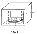
- a substrate 3 coated with a layer 4 of the crystal material is enclosed therein.
- a thin layer is of such thickness that the deformations parallel to the surface of the substrate 3 are integrally communicated to said layer over its entire thickness.
- the substrate 3 and the layer 4 are heated at a uniform temperature for a period allowing the internal stresses of the latter to be relaxed, since these internal stresses would disturb the implementation of the method and they are generally high. following the processes of usual deposit.
- the applied temperature must however leave the material of the layer 4 solid. It may be about 300 ° C for electrolytic copper deposits on silicon substrates used for the development of integrated circuits, and determined by calculation or by X-ray diffraction measurements.
- a temperature difference defined with respect to the previous temperature, is then applied to the substrate 3 and to the layer 4 at the same time as flexing by the bench 2. Stresses of double origin: bending and thermal expansion, appear. Their effects in the crystalline material of layer 4 will now be explained by the mechanics of continuous media.
- the components ⁇ of the deformations applied are due to the thermal expansions and depend on the corresponding coefficients.
- the thermal expansion of the substrate 3 is neglected in the following calculations, but it can easily be taken into account by a modification of the total deformations, since this thermal expansion of the substrate 3 returns to a boundary condition.
- the components ⁇ ij represent the elastic deformations of the layer 4.
- the components C ij are those of the tensor of the elastic constants of the crystal considered: VS 11 VS 12 VS 12 0 0 0 VS 12 VS 11 VS 12 0 0 0 VS 12 VS 12 VS 11 0 0 0 0 0 VS 44 0 0 0 0 0 0 0 0 VS 44 0 0 0 0 0 0 0 0 0 0 VS 44 0 0 0 0 0 0 0 0 0 VS 44 0 0 0 0 0 0 0 0 VS 44
- the single crystal has an axis [111] parallel to the direction x 2 .
- the tensor of a monoclinic system is given by the system (11): VS 11 VS 12 VS 13 0 VS 15 0 VS 12 VS 22 VS 23 0 VS 25 0 VS 13 VS 23 VS 33 0 VS 35 0 0 0 0 VS 44 0 VS 46 VS 15 VS 25 VS 35 0 VS 55 0 0 0 0 VS 46 0 VS 66
- the device should cover a fairly wide temperature range, typically between ambient and 500 ° C.
- the bending bench 2 would be sized to induce deformations of the order of a few thousandths.
- the oven 1 should be under vacuum or under neutral gas to prevent oxidation of the treated layers.
Landscapes
- Chemical & Material Sciences (AREA)
- Engineering & Computer Science (AREA)
- Materials Engineering (AREA)
- Metallurgy (AREA)
- Organic Chemistry (AREA)
- Chemical Kinetics & Catalysis (AREA)
- Crystallography & Structural Chemistry (AREA)
- Electrochemistry (AREA)
- General Chemical & Material Sciences (AREA)
- Crystals, And After-Treatments Of Crystals (AREA)
- Electrodes Of Semiconductors (AREA)
Description
- L'invention concerne un procédé de cristallisation dont la propriété essentielle est que l'orientation des grains du cristal est maîtrisée.
- L'orientation des grains du cristal se décide pendant sa croissance sous l'effet de phénomènes nombreux et complexes, qui dépendent d'ailleurs du procédé utilisé. Les propriétés des matériaux dépendant en général de l'orientation des grains, il peut être utile de maîtriser cette dernière. Cela concerne notamment les propriétés de conductivité électrique dans les couches minces de cuivre ou d'autres matières conductrices utilisées dans les circuits intégrés. De plus, il est souvent intéressant de maintenir une même orientation cristallographique des grains sur une grande étendue du cristal.
- L'art antérieur comporte un certain nombre de travaux tentant d'élucider les mécanismes influençant l'orientation des cristaux, mais il ne semble pas qu'un procédé simple et général de maîtrise de l'orientation des grains ait été proposé dans le cas particulier de couches minces à la surface d'un substrat.
- P. Besser et al. dans "Microstructural characterization of Inlaid copper Interconnect lines", J. of Electr. Mat., Vol 30 (2001) 320-330 décrit la recristallisation sous contrainte de ligne de cuivre pendant un recruit.
- L'objet fondamental de l'invention est de combler cette lacune. Elle concerne un procédé de cristallisation conforme à la revendication.
- L'invention sera décrite maintenant au moyen de la figure, qui représente le dispositif utilisé pour la mise en oeuvre du procédé. Il s'agit d'un four 1 incluant un banc de flexion 2. Un substrat 3 revêtu d'une couche 4 de la matière du cristal y est renfermé. Au sens de l' invention, une couche mince est d'épaisseur telle que les déformations parallèles à la surface du substrat 3 sont intégralement communiquées à ladite couche sur toute son épaisseur. Dans une première étape, le substrat 3 et la couche 4 sont chauffés à une température uniforme pendant une durée permettant de relâcher les contraintes internes de celle-ci, puisque ces contraintes internes perturberaient la mise en oeuvre du procédé et qu'elles sont généralement élevées à la suite des procédés de dépôt usuels. La température appliquée doit cependant laisser la matière de la couche 4 solide. Elle peut être d'environ 300°C pour les dépôts de cuivre électrolytique sur les substrats de silicium utilisés pour l'élaboration de circuits intégrés, et déterminée par calcul ou par des mesures par diffraction de rayons X.
- Un écart de température, défini par rapport à la température précédente, est ensuite appliqué au substrat 3 et à la couche 4 en même temps qu'une flexion par le banc 2. Des contraintes d'origine double: flexion et dilatation thermique, apparaissent. Leurs effets dans la matière cristalline de la couche 4 vont maintenant être explicités au moyen de la mécanique des milieux continus.
- On part de la relation (1) ε total = ε appliqué + ε élastique, qui exprime que, dans la couche 4, les déformations totales sont la somme des déformations appliquées par le milieu extérieur et de déformations élastiques internes. On obtient dans le cas d'un cristal cubique le système d'équations (2):
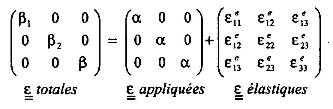
dans le repère principal défini par les vecteurs x1, x2 et x3, où x1 est dans la longueur du substrat 3 (le long de la courbure appliquée), x2 dans la largeur et x3 est normal à la surface sur laquelle la couche 4 a été déposée. Les déformations totales comprennent trois composantes, dont les deux premières sont définies par les déformations sur la face supérieure du substrat 3 puisque le substrat 3, très épais par rapport à la couche 4, lui impose ses déformations, et sont reliés par l'équation:
Les composantes α des déformations appliquées sont dues aux dilatations thermiques et dépendent des coefficients correspondants. La dilatation thermique du substrat 3 est négligée dans les calculs suivants, mais elle peut facilement être prise en compte par une modification des déformations totales, puisque cette dilatation thermique du substrat 3 revient à une condition aux limites. Par ailleurs, les composantes εij représentent les déformations élastiques de la couche 4. - On introduit maintenant un nouveau repère lié au cristal, formé de vecteurs y1, y2 et y3, et des vecteurs q', q" et q qui sont des vecteurs unitaires identiques aux vecteurs x1, x2 et x3, mais qui sont définis du point de vue de la couche 4. Les coordonnées des directions q, q' et q" dans le repère (y1, y2 y3) sont notées q1, q2 et q3; q'1, q'2 et q'3; q"1, q"2, et q"3 respectivement.
- Dans le repère (y1, y2, y3), les composantes εe 11, εe 22, εe 33, εe 33, εe 23, εe 13 et εe 12 de (2), exprimées en notation matricielle e1 à e6, valent :

avec
- La loi de Hooke σ = Cε, générale et valide dans le domaine élastique des déformations, permet de déterminer le tenseur des contraintes et notamment le vecteur de contraintes σ (q) qui s'applique sur la surface libre de la couche 4. Cela donne le système de composantes(5) exprimé dans le repère lié au cristal :

- Les composantes Cij sont celles du tenseur des constantes élastiques du cristal considéré:

- Or les composantes du système (5) doivent toutes être nulles puisque la contrainte s'appliquant sur une surface libre l'est aussi. En ajoutant membre à membre ces composantes et en remarquant que les relations (7) :

s'appliquent, les vecteurs q, q' et q" étant normaux, on obtient finalement la relation (8):
entre α, β1 et β, qui est indépendante du choix de q, q' et q". - En utilisant cette relation dans le repère lié au cristal, le système (5) de composantes devient le système (9):

pour exprimer la contrainte s'appliquant sur la surface libre de la couche 4 avec A = C 11 -C 12 -2C 44. - La condition de surface libre σ (q)=0 est forcément respectée si le cristal est isotrope, puisque alors A=0. Les matériaux usuels cristallins possèdent cependant en pratique un degré d'anisotropie, de sorte que ce sont les quantités entre crochets du système (9) qui doivent être nulles.
- L'utilisation des relations (7) permet de simplifier le système (9) et d'obtenir le système d'équations (10):

- Il n'admet de solution que pour certaines valeurs de q et q' en raison des contraintes d'orthogonalité et de normalité des vecteurs. En d'autres termes, l'application d'une déformation de flexion au substrat 3 combinée à une déformation d'origine thermique de la couche 4 permet d'une part de limiter les orientations possibles du cristal et d'autre part de l'orienter en azimut puisque l'expression des coordonnées de q' est déterminée par celle de q.
- Certains cas particuliers peuvent être discernés. Si q est parallèle à la direction [111], Q1=Q2=Q3=1/3, et on en déduit Q'1=Q'2=Q'3=1/3, c'est-à-dire que q' est aussi parallèle à [111] et donc confondu avec q, ce qui est impossible. On en déduit qu'un monocristal anisotrope du point de vue élastique ne peut pas adopter une direction de croissance de direction [111] dès lors qu'on fléchit le substrat 3. Ce résultat est valable quand le système de composantes (6) est utilisable, c'est-à-dire pour les cristaux à symétrie cubique ; il faut remarquer qu'en l'absence de flexion, la direction de croissance [111] est possible, de même que les directions de croissance [110] et [100].
- Dans un deuxième cas particulier, on choisit β1 et α de manière que β=β2 Le système (10) donne comme solution Q'1=Q'2=Q'3=1/3, et q est indéterminé. q' est donc de direction [111]. Le monocristal a un axe [111] parallèle à la direction x1.
- Dans un troisième cas, β1 et α sont choisis de manière que β = β1, on a réciproquement Q"1=Q"2=Q"3=1/3, et q encore indéterminé. q" est donc de direction [111]. Le monocristal a un axe [111] parallèle à la direction x2. Ces deux derniers exemples montrent que les cristaux peuvent être orientés en azimut autour de la direction x3 orthogonale à la couche 4 d'après les choix de β1 et α.
- Dans le cas d'une couche de cuivre ayant un coefficient de Poisson ν =0,33, des constantes élastiques C11 - 169 GPa, C12 = 122 GPa, C44 = 76 GPa et un coefficient de dilatation thermique égal à 16.10-6 K-1, si on fléchit le substrat de manière que β1 =3.10-3, la condition β =β1, du troisième cas particulier s'obtient pour α=2,16.10-3 soit ΔT = +135 °c et la condition β2 du deuxième cas particulier pour α =-0,156.10-3 soit ΔT =-10°C.
- D'autres orientations en azimut peuvent être obtenues avec d'autres variations de température. Les résultats précédents ont été obtenus pour des situations où q1, q2 et q3 sont tous les trois non nuls. Le vecteur q pourrait avoir une ou deux composantes nulles, et des résultats similaires seraient encore obtenus. Si par exemple q3=0 et q1 ≠ q2, si on choisit β1 et α de manière que β=β2, q' est la direction [001] et q (1 q') est indifférent. L'axe [001] des cristaux est alors orienté dans la direction x1 . De même, si β = β1, q" est de direction [001] et l'axe correspondant du cristal est dans la direction x2.
- Les résultats précédents peuvent être extrapolés à d'autres cristaux, les systèmes étant seulement plus compliqués puisque le tenseur d'élasticité a alors moins de composantes Cij nulles que le système (6). Par exemple, le tenseur d'un système monoclinique est donné par le système (11) :

- Dans tous les cas, il est possible d'orienter le réseau du cristal en azimut autour de la direction orthogonale à la couche cristalline d'après la température et la flexion correspondantes.
- Le dispositif devrait couvrir une gamme de température assez large, typiquement entre l'ambiante et 500°C. Le banc de flexion 2 serait dimensionné pour induire des déformations de l'ordre de quelques millièmes. Le four 1 devrait être sous vide ou sous gaz neutre afin d'éviter l'oxydation des couches traitées.
Claims (1)
- Procédé de cristallisation consistant à déposer au moins partiellement la matière du cristal sur un substrat en une couche (4) mince telle que des déformations parallèles à une surface d'un substrat (3) sur laquelle la couche (4) est déposée sont intégralement communiquées à ladite couche sur toute son épaisseur, à porter le substrat et la matière déposée sur le substrat (3) à une première température pendant une durée permettant de relâcher des contraintes internes présentes dans la matière déposée, puis à soumettre le substrat et ladite matière déposée à une seconde température et à une flexion uniforme en plaçant le substrat sur un banc (2) de flexion, une quantité de flexion et une différence entre la première et la seconde température ayant des valeurs déterminées à partir de relations faisant intervenir des constantes élastiques (Cij ) de flexion, des déformations thermiques (x) et des coefficients de dilatation thermique pour favoriser une orientation cristallographique particulière de la matière déposée selon une direction d'azimut par rapport à une direction normale au substrat définie par le système

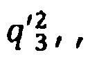
où β1, β2 et β sont des déformations totales subies par la couche (4) dans des directions de longueur, correspondant à une courbure associée à la flexion, de largeur et d'épaisseur de la couche (4), et Q1, Q2, Q3, Q'1, Q'2 et Q'3 sont égaux
Applications Claiming Priority (1)
| Application Number | Priority Date | Filing Date | Title |
|---|---|---|---|
| FR0950892A FR2941968B1 (fr) | 2009-02-12 | 2009-02-12 | Procede de cristallisation avec maitrise de l'orientation des grains du cristal |
Publications (2)
| Publication Number | Publication Date |
|---|---|
| EP2218805A1 EP2218805A1 (fr) | 2010-08-18 |
| EP2218805B1 true EP2218805B1 (fr) | 2012-03-14 |
Family
ID=41110538
Family Applications (1)
| Application Number | Title | Priority Date | Filing Date |
|---|---|---|---|
| EP10152945A Not-in-force EP2218805B1 (fr) | 2009-02-12 | 2010-02-08 | Procédé de cristallisation avec maîtrise de l'orientation des grains du cristal |
Country Status (5)
| Country | Link |
|---|---|
| US (1) | US8586127B2 (fr) |
| EP (1) | EP2218805B1 (fr) |
| JP (1) | JP2010189257A (fr) |
| AT (1) | ATE549436T1 (fr) |
| FR (1) | FR2941968B1 (fr) |
Families Citing this family (2)
| Publication number | Priority date | Publication date | Assignee | Title |
|---|---|---|---|---|
| JP7519171B2 (ja) * | 2019-06-17 | 2024-07-19 | 日本特殊陶業株式会社 | 静電チャックおよびその運転方法 |
| CN114823285B (zh) * | 2022-04-07 | 2025-02-18 | 浙江清华柔性电子技术研究院 | 超薄芯片及其平整化方法和应用 |
Family Cites Families (5)
| Publication number | Priority date | Publication date | Assignee | Title |
|---|---|---|---|---|
| SU966122A1 (ru) * | 1980-08-20 | 1982-10-15 | Тамбовский институт химического машиностроения | Способ залечивани трещин в щелочно-галоидных кристаллах |
| JPH02239198A (ja) * | 1989-03-08 | 1990-09-21 | Nec Corp | 転位制御方法 |
| US6479625B1 (en) * | 2002-05-28 | 2002-11-12 | Agri-Nutrients Technology Group, Inc. | Mechanical stress crystallization of thermoplastic polymers |
| JP2007242826A (ja) * | 2006-03-08 | 2007-09-20 | Mitsubishi Heavy Ind Ltd | 成膜装置及び成膜方法 |
| FR2911130B1 (fr) * | 2007-01-05 | 2009-11-27 | Saint Gobain | Procede de depot de couche mince et produit obtenu |
-
2009
- 2009-02-12 FR FR0950892A patent/FR2941968B1/fr not_active Expired - Fee Related
-
2010
- 2010-01-20 US US12/690,414 patent/US8586127B2/en not_active Expired - Fee Related
- 2010-02-08 EP EP10152945A patent/EP2218805B1/fr not_active Not-in-force
- 2010-02-08 AT AT10152945T patent/ATE549436T1/de active
- 2010-02-10 JP JP2010027842A patent/JP2010189257A/ja active Pending
Also Published As
| Publication number | Publication date |
|---|---|
| ATE549436T1 (de) | 2012-03-15 |
| EP2218805A1 (fr) | 2010-08-18 |
| FR2941968A1 (fr) | 2010-08-13 |
| US8586127B2 (en) | 2013-11-19 |
| US20100203233A1 (en) | 2010-08-12 |
| FR2941968B1 (fr) | 2012-01-06 |
| JP2010189257A (ja) | 2010-09-02 |
Similar Documents
| Publication | Publication Date | Title |
|---|---|---|
| Bartolomeo et al. | Graphene field effect transistors with niobium contacts and asymmetric transfer characteristics | |
| Liaw et al. | The characterization of sputtered polycrystalline aluminum nitride on silicon by surface acoustic wave measurements | |
| Mondal et al. | Unprecedented enhancement of piezoelectricity of wurtzite nitride semiconductors via thermal annealing | |
| Sidorov et al. | Density of dislocations in CdHgTe heteroepitaxial structures on GaAs (013) and Si (013) substrates | |
| Xie et al. | Effect of Mg doping on the structural and free-charge carrier properties of InN films | |
| EP2218805A1 (fr) | Procédé de cristallisation avec maîtrise de l'orientation des grains du cristal | |
| Jinno et al. | Strain Relaxation of Al‐Rich α‐(AlGa) 2O3 and α‐Al2O3/Ga2O3 Superlattice on m‐Plane Sapphire Substrates by Plasma‐Assisted Molecular Beam Epitaxy | |
| Liu et al. | Epitaxial strain and its relaxation at the LaAlO3/SrTiO3 interface | |
| Dutheil et al. | AlN, ZnO thin films and AlN/ZnO or ZnO/AlN multilayer structures deposited by PLD for surface acoustic wave applications | |
| Kaneko et al. | Large constriction of lattice constant in epitaxial magnesium oxide thin film: Effect of point defects on lattice constant | |
| Riobóo et al. | Hypersonic characterization of sound propagation velocity in Al x Ga 1− x N thin films | |
| Chauveau et al. | Anisotropic strain effects on the photoluminescence emission from heteroepitaxial and homoepitaxial nonpolar (Zn, Mg) O/ZnO quantum wells | |
| Chakraborty et al. | A full-field crystal plasticity study on how texture and grain structure influences hydrostatic stress in thermally strained β-Sn films | |
| Yamada et al. | Strong growth orientation dependence of strain relaxation in epitaxial (Ba, Sr) TiO3 films and the resulting dielectric properties | |
| WO2024200842A1 (fr) | Procédé de fabrication d'une association de matériaux piézoélectrique et magnétostrictif pour l' obtention d' un matériau composite magnétoélectrique exhibant un comportement auto-polarisé | |
| Hayashi et al. | Thermal strain analysis considering in-plane anisotropy for sputtered AlN on c-and a-plane sapphire under high-temperature annealing | |
| Banal et al. | Nanometer‐thin ALD‐Al2O3 for the improvement of the structural quality of AlN grown on sapphire substrate by MOVPE | |
| Polat et al. | Identifying threading dislocations in CdTe films by reciprocal space mapping and defect decoration etching | |
| Kyutt et al. | X‐ray diffraction study of strain and defect structure of nonpolar a‐plane GaN‐layers grown on r‐plane sapphire | |
| Azrak et al. | Aluminium-nitride thin-films on polymer substrates obtained by adhesive bonding | |
| Grabov et al. | The use of the method of zone recrystallization under a coating for preparing single-crystal films of bismuth-antimony solid solution | |
| Grabov et al. | Atomic-force microscopy of bismuth film defects decorated by oxidation | |
| Shaldin et al. | Pyroelectric properties of real LiNbO3 single crystals grown from a congruent melt | |
| Singh et al. | Reversal of strain state in a Mott insulator thin film by controlling substrate morphology | |
| US7348201B2 (en) | Creation of anisotropic strain in semiconductor quantum well |
Legal Events
| Date | Code | Title | Description |
|---|---|---|---|
| PUAI | Public reference made under article 153(3) epc to a published international application that has entered the european phase |
Free format text: ORIGINAL CODE: 0009012 |
|
| AK | Designated contracting states |
Kind code of ref document: A1 Designated state(s): AT BE BG CH CY CZ DE DK EE ES FI FR GB GR HR HU IE IS IT LI LT LU LV MC MK MT NL NO PL PT RO SE SI SK SM TR |
|
| 17P | Request for examination filed |
Effective date: 20110216 |
|
| 17Q | First examination report despatched |
Effective date: 20110328 |
|
| RIC1 | Information provided on ipc code assigned before grant |
Ipc: C30B 33/02 20060101ALI20110803BHEP Ipc: C30B 33/00 20060101ALI20110803BHEP Ipc: C25D 5/50 20060101AFI20110803BHEP Ipc: C30B 29/02 20060101ALI20110803BHEP |
|
| GRAP | Despatch of communication of intention to grant a patent |
Free format text: ORIGINAL CODE: EPIDOSNIGR1 |
|
| GRAS | Grant fee paid |
Free format text: ORIGINAL CODE: EPIDOSNIGR3 |
|
| GRAA | (expected) grant |
Free format text: ORIGINAL CODE: 0009210 |
|
| AK | Designated contracting states |
Kind code of ref document: B1 Designated state(s): AT BE BG CH CY CZ DE DK EE ES FI FR GB GR HR HU IE IS IT LI LT LU LV MC MK MT NL NO PL PT RO SE SI SK SM TR |
|
| REG | Reference to a national code |
Ref country code: GB Ref legal event code: FG4D Free format text: NOT ENGLISH |
|
| REG | Reference to a national code |
Ref country code: AT Ref legal event code: REF Ref document number: 549436 Country of ref document: AT Kind code of ref document: T Effective date: 20120315 Ref country code: CH Ref legal event code: EP |
|
| REG | Reference to a national code |
Ref country code: IE Ref legal event code: FG4D Free format text: LANGUAGE OF EP DOCUMENT: FRENCH |
|
| REG | Reference to a national code |
Ref country code: DE Ref legal event code: R096 Ref document number: 602010000979 Country of ref document: DE Effective date: 20120510 |
|
| REG | Reference to a national code |
Ref country code: NL Ref legal event code: T3 |
|
| PG25 | Lapsed in a contracting state [announced via postgrant information from national office to epo] |
Ref country code: LT Free format text: LAPSE BECAUSE OF FAILURE TO SUBMIT A TRANSLATION OF THE DESCRIPTION OR TO PAY THE FEE WITHIN THE PRESCRIBED TIME-LIMIT Effective date: 20120314 Ref country code: NO Free format text: LAPSE BECAUSE OF FAILURE TO SUBMIT A TRANSLATION OF THE DESCRIPTION OR TO PAY THE FEE WITHIN THE PRESCRIBED TIME-LIMIT Effective date: 20120614 Ref country code: HR Free format text: LAPSE BECAUSE OF FAILURE TO SUBMIT A TRANSLATION OF THE DESCRIPTION OR TO PAY THE FEE WITHIN THE PRESCRIBED TIME-LIMIT Effective date: 20120314 |
|
| LTIE | Lt: invalidation of european patent or patent extension |
Effective date: 20120314 |
|
| PG25 | Lapsed in a contracting state [announced via postgrant information from national office to epo] |
Ref country code: FI Free format text: LAPSE BECAUSE OF FAILURE TO SUBMIT A TRANSLATION OF THE DESCRIPTION OR TO PAY THE FEE WITHIN THE PRESCRIBED TIME-LIMIT Effective date: 20120314 Ref country code: LV Free format text: LAPSE BECAUSE OF FAILURE TO SUBMIT A TRANSLATION OF THE DESCRIPTION OR TO PAY THE FEE WITHIN THE PRESCRIBED TIME-LIMIT Effective date: 20120314 Ref country code: GR Free format text: LAPSE BECAUSE OF FAILURE TO SUBMIT A TRANSLATION OF THE DESCRIPTION OR TO PAY THE FEE WITHIN THE PRESCRIBED TIME-LIMIT Effective date: 20120615 |
|
| REG | Reference to a national code |
Ref country code: AT Ref legal event code: MK05 Ref document number: 549436 Country of ref document: AT Kind code of ref document: T Effective date: 20120314 |
|
| PG25 | Lapsed in a contracting state [announced via postgrant information from national office to epo] |
Ref country code: CY Free format text: LAPSE BECAUSE OF FAILURE TO SUBMIT A TRANSLATION OF THE DESCRIPTION OR TO PAY THE FEE WITHIN THE PRESCRIBED TIME-LIMIT Effective date: 20120314 |
|
| PG25 | Lapsed in a contracting state [announced via postgrant information from national office to epo] |
Ref country code: PL Free format text: LAPSE BECAUSE OF FAILURE TO SUBMIT A TRANSLATION OF THE DESCRIPTION OR TO PAY THE FEE WITHIN THE PRESCRIBED TIME-LIMIT Effective date: 20120314 Ref country code: SE Free format text: LAPSE BECAUSE OF FAILURE TO SUBMIT A TRANSLATION OF THE DESCRIPTION OR TO PAY THE FEE WITHIN THE PRESCRIBED TIME-LIMIT Effective date: 20120314 Ref country code: RO Free format text: LAPSE BECAUSE OF FAILURE TO SUBMIT A TRANSLATION OF THE DESCRIPTION OR TO PAY THE FEE WITHIN THE PRESCRIBED TIME-LIMIT Effective date: 20120314 Ref country code: IS Free format text: LAPSE BECAUSE OF FAILURE TO SUBMIT A TRANSLATION OF THE DESCRIPTION OR TO PAY THE FEE WITHIN THE PRESCRIBED TIME-LIMIT Effective date: 20120714 Ref country code: EE Free format text: LAPSE BECAUSE OF FAILURE TO SUBMIT A TRANSLATION OF THE DESCRIPTION OR TO PAY THE FEE WITHIN THE PRESCRIBED TIME-LIMIT Effective date: 20120314 Ref country code: CZ Free format text: LAPSE BECAUSE OF FAILURE TO SUBMIT A TRANSLATION OF THE DESCRIPTION OR TO PAY THE FEE WITHIN THE PRESCRIBED TIME-LIMIT Effective date: 20120314 Ref country code: SI Free format text: LAPSE BECAUSE OF FAILURE TO SUBMIT A TRANSLATION OF THE DESCRIPTION OR TO PAY THE FEE WITHIN THE PRESCRIBED TIME-LIMIT Effective date: 20120314 |
|
| PG25 | Lapsed in a contracting state [announced via postgrant information from national office to epo] |
Ref country code: SK Free format text: LAPSE BECAUSE OF FAILURE TO SUBMIT A TRANSLATION OF THE DESCRIPTION OR TO PAY THE FEE WITHIN THE PRESCRIBED TIME-LIMIT Effective date: 20120314 Ref country code: PT Free format text: LAPSE BECAUSE OF FAILURE TO SUBMIT A TRANSLATION OF THE DESCRIPTION OR TO PAY THE FEE WITHIN THE PRESCRIBED TIME-LIMIT Effective date: 20120716 |
|
| PLBE | No opposition filed within time limit |
Free format text: ORIGINAL CODE: 0009261 |
|
| STAA | Information on the status of an ep patent application or granted ep patent |
Free format text: STATUS: NO OPPOSITION FILED WITHIN TIME LIMIT |
|
| PG25 | Lapsed in a contracting state [announced via postgrant information from national office to epo] |
Ref country code: DK Free format text: LAPSE BECAUSE OF FAILURE TO SUBMIT A TRANSLATION OF THE DESCRIPTION OR TO PAY THE FEE WITHIN THE PRESCRIBED TIME-LIMIT Effective date: 20120314 Ref country code: AT Free format text: LAPSE BECAUSE OF FAILURE TO SUBMIT A TRANSLATION OF THE DESCRIPTION OR TO PAY THE FEE WITHIN THE PRESCRIBED TIME-LIMIT Effective date: 20120314 |
|
| 26N | No opposition filed |
Effective date: 20121217 |
|
| PG25 | Lapsed in a contracting state [announced via postgrant information from national office to epo] |
Ref country code: IT Free format text: LAPSE BECAUSE OF FAILURE TO SUBMIT A TRANSLATION OF THE DESCRIPTION OR TO PAY THE FEE WITHIN THE PRESCRIBED TIME-LIMIT Effective date: 20120314 |
|
| REG | Reference to a national code |
Ref country code: DE Ref legal event code: R097 Ref document number: 602010000979 Country of ref document: DE Effective date: 20121217 |
|
| PG25 | Lapsed in a contracting state [announced via postgrant information from national office to epo] |
Ref country code: ES Free format text: LAPSE BECAUSE OF FAILURE TO SUBMIT A TRANSLATION OF THE DESCRIPTION OR TO PAY THE FEE WITHIN THE PRESCRIBED TIME-LIMIT Effective date: 20120625 |
|
| PGFP | Annual fee paid to national office [announced via postgrant information from national office to epo] |
Ref country code: NL Payment date: 20130115 Year of fee payment: 4 |
|
| PG25 | Lapsed in a contracting state [announced via postgrant information from national office to epo] |
Ref country code: BG Free format text: LAPSE BECAUSE OF FAILURE TO SUBMIT A TRANSLATION OF THE DESCRIPTION OR TO PAY THE FEE WITHIN THE PRESCRIBED TIME-LIMIT Effective date: 20120614 |
|
| BERE | Be: lapsed |
Owner name: COMMISSARIAT A L'ENERGIE ATOMIQUE ET AUX ENERGIES Effective date: 20130228 |
|
| PG25 | Lapsed in a contracting state [announced via postgrant information from national office to epo] |
Ref country code: MC Free format text: LAPSE BECAUSE OF NON-PAYMENT OF DUE FEES Effective date: 20130228 |
|
| REG | Reference to a national code |
Ref country code: IE Ref legal event code: MM4A |
|
| PG25 | Lapsed in a contracting state [announced via postgrant information from national office to epo] |
Ref country code: BE Free format text: LAPSE BECAUSE OF NON-PAYMENT OF DUE FEES Effective date: 20130228 Ref country code: IE Free format text: LAPSE BECAUSE OF NON-PAYMENT OF DUE FEES Effective date: 20130208 |
|
| PGFP | Annual fee paid to national office [announced via postgrant information from national office to epo] |
Ref country code: DE Payment date: 20140211 Year of fee payment: 5 |
|
| PGFP | Annual fee paid to national office [announced via postgrant information from national office to epo] |
Ref country code: FR Payment date: 20140228 Year of fee payment: 5 |
|
| PG25 | Lapsed in a contracting state [announced via postgrant information from national office to epo] |
Ref country code: MT Free format text: LAPSE BECAUSE OF FAILURE TO SUBMIT A TRANSLATION OF THE DESCRIPTION OR TO PAY THE FEE WITHIN THE PRESCRIBED TIME-LIMIT Effective date: 20120314 |
|
| PGFP | Annual fee paid to national office [announced via postgrant information from national office to epo] |
Ref country code: GB Payment date: 20140219 Year of fee payment: 5 |
|
| REG | Reference to a national code |
Ref country code: NL Ref legal event code: V1 Effective date: 20140901 |
|
| REG | Reference to a national code |
Ref country code: CH Ref legal event code: PL |
|
| PG25 | Lapsed in a contracting state [announced via postgrant information from national office to epo] |
Ref country code: CH Free format text: LAPSE BECAUSE OF NON-PAYMENT OF DUE FEES Effective date: 20140228 Ref country code: LI Free format text: LAPSE BECAUSE OF NON-PAYMENT OF DUE FEES Effective date: 20140228 Ref country code: NL Free format text: LAPSE BECAUSE OF NON-PAYMENT OF DUE FEES Effective date: 20140901 |
|
| PG25 | Lapsed in a contracting state [announced via postgrant information from national office to epo] |
Ref country code: SM Free format text: LAPSE BECAUSE OF FAILURE TO SUBMIT A TRANSLATION OF THE DESCRIPTION OR TO PAY THE FEE WITHIN THE PRESCRIBED TIME-LIMIT Effective date: 20120314 |
|
| PG25 | Lapsed in a contracting state [announced via postgrant information from national office to epo] |
Ref country code: TR Free format text: LAPSE BECAUSE OF FAILURE TO SUBMIT A TRANSLATION OF THE DESCRIPTION OR TO PAY THE FEE WITHIN THE PRESCRIBED TIME-LIMIT Effective date: 20120314 |
|
| PG25 | Lapsed in a contracting state [announced via postgrant information from national office to epo] |
Ref country code: MK Free format text: LAPSE BECAUSE OF FAILURE TO SUBMIT A TRANSLATION OF THE DESCRIPTION OR TO PAY THE FEE WITHIN THE PRESCRIBED TIME-LIMIT Effective date: 20120314 Ref country code: LU Free format text: LAPSE BECAUSE OF NON-PAYMENT OF DUE FEES Effective date: 20130208 Ref country code: HU Free format text: LAPSE BECAUSE OF FAILURE TO SUBMIT A TRANSLATION OF THE DESCRIPTION OR TO PAY THE FEE WITHIN THE PRESCRIBED TIME-LIMIT; INVALID AB INITIO Effective date: 20100208 |
|
| REG | Reference to a national code |
Ref country code: DE Ref legal event code: R119 Ref document number: 602010000979 Country of ref document: DE |
|
| GBPC | Gb: european patent ceased through non-payment of renewal fee |
Effective date: 20150208 |
|
| REG | Reference to a national code |
Ref country code: FR Ref legal event code: ST Effective date: 20151030 |
|
| PG25 | Lapsed in a contracting state [announced via postgrant information from national office to epo] |
Ref country code: DE Free format text: LAPSE BECAUSE OF NON-PAYMENT OF DUE FEES Effective date: 20150901 Ref country code: GB Free format text: LAPSE BECAUSE OF NON-PAYMENT OF DUE FEES Effective date: 20150208 |
|
| PG25 | Lapsed in a contracting state [announced via postgrant information from national office to epo] |
Ref country code: FR Free format text: LAPSE BECAUSE OF NON-PAYMENT OF DUE FEES Effective date: 20150302 |