EP2216803A1 - Manufacturing method for laminated substrate - Google Patents
Manufacturing method for laminated substrate Download PDFInfo
- Publication number
- EP2216803A1 EP2216803A1 EP08853796A EP08853796A EP2216803A1 EP 2216803 A1 EP2216803 A1 EP 2216803A1 EP 08853796 A EP08853796 A EP 08853796A EP 08853796 A EP08853796 A EP 08853796A EP 2216803 A1 EP2216803 A1 EP 2216803A1
- Authority
- EP
- European Patent Office
- Prior art keywords
- film
- donor wafer
- substrate
- bonded
- wafer
- Prior art date
- Legal status (The legal status is an assumption and is not a legal conclusion. Google has not performed a legal analysis and makes no representation as to the accuracy of the status listed.)
- Granted
Links
Images
Classifications
-
- H—ELECTRICITY
- H10—SEMICONDUCTOR DEVICES; ELECTRIC SOLID-STATE DEVICES NOT OTHERWISE PROVIDED FOR
- H10D—INORGANIC ELECTRIC SEMICONDUCTOR DEVICES
- H10D86/00—Integrated devices formed in or on insulating or conducting substrates, e.g. formed in silicon-on-insulator [SOI] substrates or on stainless steel or glass substrates
- H10D86/201—Integrated devices formed in or on insulating or conducting substrates, e.g. formed in silicon-on-insulator [SOI] substrates or on stainless steel or glass substrates the substrates comprising an insulating layer on a semiconductor body, e.g. SOI
-
- H—ELECTRICITY
- H10—SEMICONDUCTOR DEVICES; ELECTRIC SOLID-STATE DEVICES NOT OTHERWISE PROVIDED FOR
- H10P—GENERIC PROCESSES OR APPARATUS FOR THE MANUFACTURE OR TREATMENT OF DEVICES COVERED BY CLASS H10
- H10P10/00—Bonding of wafers, substrates or parts of devices
- H10P10/12—Bonding of semiconductor wafers or semiconductor substrates to semiconductor wafers or semiconductor substrates
- H10P10/128—Bonding of semiconductor wafers or semiconductor substrates to semiconductor wafers or semiconductor substrates by direct semiconductor to semiconductor bonding
-
- H—ELECTRICITY
- H10—SEMICONDUCTOR DEVICES; ELECTRIC SOLID-STATE DEVICES NOT OTHERWISE PROVIDED FOR
- H10P—GENERIC PROCESSES OR APPARATUS FOR THE MANUFACTURE OR TREATMENT OF DEVICES COVERED BY CLASS H10
- H10P90/00—Preparation of wafers not covered by a single main group of this subclass, e.g. wafer reinforcement
- H10P90/19—Preparing inhomogeneous wafers
- H10P90/1904—Preparing vertically inhomogeneous wafers
- H10P90/1906—Preparing SOI wafers
- H10P90/1914—Preparing SOI wafers using bonding
- H10P90/1916—Preparing SOI wafers using bonding with separation or delamination along an ion implanted layer, e.g. Smart-cut
-
- H—ELECTRICITY
- H10—SEMICONDUCTOR DEVICES; ELECTRIC SOLID-STATE DEVICES NOT OTHERWISE PROVIDED FOR
- H10W—GENERIC PACKAGES, INTERCONNECTIONS, CONNECTORS OR OTHER CONSTRUCTIONAL DETAILS OF DEVICES COVERED BY CLASS H10
- H10W10/00—Isolation regions in semiconductor bodies between components of integrated devices
- H10W10/10—Isolation regions comprising dielectric materials
- H10W10/181—Semiconductor-on-insulator [SOI] isolation regions, e.g. buried oxide regions of SOI wafers
-
- H—ELECTRICITY
- H10—SEMICONDUCTOR DEVICES; ELECTRIC SOLID-STATE DEVICES NOT OTHERWISE PROVIDED FOR
- H10D—INORGANIC ELECTRIC SEMICONDUCTOR DEVICES
- H10D30/00—Field-effect transistors [FET]
- H10D30/60—Insulated-gate field-effect transistors [IGFET]
- H10D30/751—Insulated-gate field-effect transistors [IGFET] having composition variations in the channel regions
Definitions
- the present invention relates to a method for producing a bonded substrate.
- the present invention relates to a method for producing a bonded substrate comprising a Si 1-x Ge x (wherein x is a number satisfying O ⁇ x ⁇ 51) film in which a biaxial strain has been introduced.
- a strained silicon substrate in which a strain is induced in a silicon layer has been proposed in addition to a conventional bulk silicon wafer and silicon-on-insulator (SOI).
- SOI silicon-on-insulator
- a SiGe layer containing 15% to 20% germanium (molar concentration) is epitaxially grown on a silicon wafer, and silicon is epitaxially grown on the SiGe layer to obtain a strained silicon layer (see, for example, Non-Patent Reference 1).
- the method is characterized in that, since the lattice constant of the SiGe layer is larger than the lattice constant of the silicon layer, a biaxial strain is laterally introduced in the silicon layer epitaxially grown on the SiGe layer. Accordingly, the mobility of electrons is increased.
- the present invention provides a method for producing a bonded substrate, the method being able to easily produce a bonded substrate comprising a SiGe film or Ge film (hereinafter, may also be referred to as a Si 1-x Ge x film (wherein x is a number satisfying 0 ⁇ x ⁇ 1)) in which a larger biaxial strain has been introduced than ever.
- a SiGe film or Ge film hereinafter, may also be referred to as a Si 1-x Ge x film (wherein x is a number satisfying 0 ⁇ x ⁇ 1)
- the present invention provides a method for producing a bonded substrate, comprising at least the steps of: providing a donor wafer and a handle wafer having a thermal expansion coefficient lower than the donor wafer, implanting ions of any one or both of hydrogen and a noble gas into the donor wafer to form an ion-implanted layer, performing a surface activation treatment on at least one of bonding surfaces of the donor wafer and the handle wafer, bonding the donor wafer to the handle wafer, thinning the donor wafer by splitting the donor wafer through application of a mechanical impact to the ion-implanted layer of the donor wafer, performing a surface treatment on a split surface of the thinned donor wafer, and epitaxially growing a Si 1-x Ge x (0 ⁇ x ⁇ 1) film on the split surface to form a strained Si 1-x Ge x (0 ⁇ x ⁇ 1) film on the bonded wafers.
- the production method of the present invention are characterized in that: the ion-implanted donor wafer is bonded to the handle wafer having a thermal expansion coefficient lower than the donor wafer, the surface activation treatment is performed to increase the bonding strength and then the wafers are bonded together, the donor wafer is thinned by splitting the donor wafer along the ion-implanted layer through the application of a mechanical impact, the surface treatment is performed on the split surface of the thinned donor wafer, and thereafter the Si 1-x Ge x (0 ⁇ x ⁇ 1) film is epitaxially grown on the split surface.
- the Si 1-x Ge x (0 ⁇ x ⁇ 1) film is epitaxially grown, the bonded wafers are heated.
- the donor wafer tries to expand more than the handle wafer because the donor wafer has a thermal expansion coefficient higher than the handle wafer.
- the donor wafer is not allowed to expand in such a manner that the donor wafer is pulled by the handle wafer.
- the biaxial strain in the Si 1-x Ge x (0 ⁇ x ⁇ 1) film formed on the donor wafer is relaxed at the temperature during the epitaxial growth, and the Si 1-x Ge x (0 ⁇ x ⁇ 1) film tries to contract when cooled after the epitaxial growth.
- the handle wafer has a thermal expansion coefficient lower than the donor wafer, the handle wafer hardly contracts.
- the sufficiently high bonding strength as described above does not allow the Si 1-x Ge x (0 ⁇ x ⁇ 1) film to contract in such a way that the Si 1-x Ge x (0 ⁇ x ⁇ 1) film follows the manner of the handle wafer. In this way, a large biaxial strain is introduced in the epitaxially grown Si 1-x Ge x (0 ⁇ x ⁇ 1) film. Hence, it is possible to obtain a bonded substrate comprising a Si 1-x Ge x (0 ⁇ x ⁇ 1) film in which a large biaxial strain has been introduced.
- the strained Si 1-x Ge x , (0 ⁇ x ⁇ 1) film can be formed on a newly provided silicon substrate or a newly provided silicon substrate with an oxide film thereon as follows. Specifically, a bonded substrate produced by the above method is bonded to the newly provided silicon substrate or the newly provided silicon substrate with an oxide film thereon. Then, the strained Si 1-x Ge x (0 ⁇ x ⁇ 1) film is transferred to the newly provided silicon substrate or newly provided silicon substrate with an oxide film thereon. In this manner, it is possible to obtain a bonded substrate comprising a strained Si 1-x Ge x (0 ⁇ x ⁇ 1) film on a silicon substrate, the strained Si 1-x Ge x (0 ⁇ x ⁇ 1) film having a large biaxial strain introduced therein.
- a large biaxial strain can be introduced in a Si 1-x Ge x (0 ⁇ x ⁇ 1) film more easily in comparison with a conventional method. This makes it possible to produce a bonded substrate comprising the Si 1-x Ge x (0 ⁇ x ⁇ 1) film in which the large biaxial strain has been introduced.
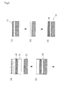
- FIG. 1 shows process drawings illustrating one example of steps in a method for producing a bonded substrate of the present invention.
- the present inventors have earnestly studied a method for producing a bonded substrate in which a larger biaxial strain has been efficiently introduced in comparison with a conventional strained Si 1-x Ge x (0 ⁇ x ⁇ 1) film.
- a large biaxial strain is introduced in a Si 1-x Ge x (0 ⁇ x ⁇ 1) film epitaxially grown on a donor wafer after the donor wafer is bonded to a handle wafer made of a material having a thermal expansion coefficient lower than the donor wafer.
- the bonded substrate of the present invention comprises at least a quartz substrate, a silicon film and a Si 1-x Ge x (0 ⁇ x ⁇ 1) film.
- the silicon film is a film thinned by splitting after the quartz substrate is bonded thereto.
- the strained Si 1-x Ge x (0 ⁇ x ⁇ 1) film is epitaxially grown on the silicon film.
- Such a bonded substrate is obtained by the method for producing a bonded substrate in the present invention described below, using the quartz substrate as the handle wafer and using a silicon substrate as the donor wafer.
- Fig. 1 shows process drawings illustrating one example of steps in the method for producing a bonded substrate of the present invention.
- Step a providing donor and handle wafers, implanting ions into donor wafer
- ions of any one or both of hydrogen and a noble gas are implanted into one surface of the donor wafer 11 to form an ion-implanted layer 13.
- a silicon substrate or a silicon substrate with an oxide film thereon can preferably be used as the donor wafer 11.
- the preferable thickness of the donor wafer is not particularly limited but is desirably approximate to the thickness of a silicon wafer standardized by SEMI or the like. This is because semiconductor devices are often designed to use a wafer of this thickness. From this viewpoint, the thickness is preferably 300 to 900 ⁇ m.
- the silicon oxide film of the silicon substrate with an oxide film thereon preferably has a thickness of 50 to 500 nm.
- the silicon oxide film can be formed by a generally-accepted thermal oxidation method. However, if the silicon oxide film is too thin, it is difficult to control the thickness of the oxide film.
- the thickness is too thick, it takes a longer time to form such a silicon oxide film.
- an effect of suppressing channeling of the implanted ions is obtained.
- the silicon substrate or the silicon substrate with an oxide film thereon as described above is used as the donor wafer, a Si 1-x Ge x (0 ⁇ x ⁇ 1) film can be epitaxially grown on the surface of silicon having a lattice constant smaller than Si 1-x Ge x (0 ⁇ x ⁇ 1) has. Accordingly, a larger biaxial strain can be easily introduced in the Si 1-x Ge x (0 ⁇ x ⁇ 1) film during the substrate cooling after the epitaxial growth.
- a quartz substrate can preferably be used as the handle wafer 12.
- quartz having a thermal expansion coefficient (5x10 -7 /K) lower than silicon and germanium have is used as the handle wafer in this manner, a larger biaxial strain can be introduced in the Si 1-x Ge x (0 ⁇ x ⁇ 1) film, Moreover, quartz has an advantage that impurities are hardly introduced in the Si 1-x Ge x layer.
- a material having a thermal expansion coefficient of 1.3 ⁇ 10 -6 (/K) or lower can preferably be used as the handle wafer 12, Thermal expansion coefficient can be measured based on Japanese Industrial Standards (JIS) R 1618.
- JIS Japanese Industrial Standards
- a larger biaxial strain can be introduced into the Si 1-x Ge x (0 ⁇ x ⁇ 1) film.
- the implantation energy, implantation dose, implantation temperature and other ion implantation conditions can also be appropriately selected so as to obtain the film having a predetermined thickness.
- the temperature of the substrate during the implantation may be 250°C to 400°C
- the ion implantation depth may be 0.5 ⁇ m
- the implantation energy may be 20 to 100 keV
- the implantation dose may be 1 ⁇ 10 16 to 1 ⁇ 10 17 /cm 2 .
- the ion implantation conditions are not limited thereto.
- Step b performing surface activation treatment, bonding wafers
- At least one of bonding surfaces of the donor wafer 11 and the handle wafer 12 is subjected to, for example, a plasma activation treatment or an ozone treatment as a surface activation treatment. Then, the bonding surface of the donor wafer 11 is closely adhered to the bonding surface of the handle wafer 12 for bonding In this event, since at least one of the bonding surfaces of the donor wafer 11 and the handle wafer 12 has been subjected to the surface activation treatment, the bonding strength at a bonded surface 14 therebetween is sufficiently high.
- a plasma treatment can be performed as the surface activation treatment.
- the plasma treatment is performed as the surface activation treatment in the above manner, the surface of the substrate subjected to the surface activation treatment is activated, for example, in a way that the number of OH groups on the surface is increased. Accordingly, when the handle wafer 12 is closely adhered to the ion-implanted surface of the donor wafer 11 in this state, the wafers can be strongly bonded together with a hydrogen bond and so forth.
- an ozone treatment or the like can be performed as the surface activation treatment, or several types of treatments may be performed in combination.
- the plasma treatment is preferably performed as follows. Specifically, a substrate cleaned by RCA cleaning or the like is placed in a vacuum chamber. After a plasma gas is introduced therein, the substrate is exposed to a high-frequency plasma of preferably approximately 100 W for approximately 5 to 30 seconds. Thus, the surface of the substrate is subjected to the plasma treatment.
- the plasma gas can include an oxygen gas plasma for treating a silicon substrate with an oxide film thereon; and a hydrogen gas, an argon gas, a mixed gas of a hydrogen gas and an argon gas, or a mixed gas of a hydrogen gas and a helium gas for treating a silicon substrate. Meanwhile, a nitrogen gas that is an inert gas may be used.
- the ozone treatment is preferably performed as follows. Specifically, a substrate cleaned by RCA cleaning or the like is placed in a chamber in which an air has been introduced. After a plasma gas such as a nitrogen gas or an argon gas is introduced therein, a high-frequency plasma is generated to convert oxygen in the air into ozone. Thus, the surface of the substrate is subjected to the ozone treatment.
- a plasma gas such as a nitrogen gas or an argon gas
- the substrates can be strongly bonded together without high temperature treatment when the surface subjected to the surface activation treatment as described above is used as the bonding surface and the substrates are closely adhered together, for example, under a reduced pressure or normal pressure at room temperature.
- a heat treatment in a temperature range of 100°C to 350°C can be preferably performed on the bonded wafers.
- a higher strength of bonding between the donor wafer and the handle wafer can be achieved.
- this can further reduce the possibility that a bonding defect occurs between the bonded wafers in the subsequent steps such as a step of splitting and a step of epitaxially growing the Si 1-x Ge x (0 ⁇ x ⁇ 1) film.
- the donor wafer 11 is thinned by splitting the donor wafer 11 along the ion-implanted layer 13 preferably through application of a mechanical impact to the ion-implanted layer 13.
- the thickness of the thinned donor wafer is preferably 300 to 500 nm, and further preferably approximately 400 nm, although depending on the depth to the ion-implanted layer from the wafer surface from which the ions are implanted.
- the thickness of the ion-implanted layer is favorably a thickness which easily allows the splitting by the mechanical impact.
- the thickness is preferably 200 to 400 nm, and further preferably approximately 300 nm,
- Step d performing surface treatment
- a surface treatment is performed on a split surface 15 of the thinned donor wafer. Thereby, an ion-implanted damaged layer remained in the split surface 15 is removed,
- At least one treatment of a polishing treatment, a heat treatment and an etching treatment can preferably be performed as the surface treatment.
- the heat treatment and the etching treatment is performed as the surface treatment, the ion-implanted damaged layer which is present in the split surface of the donor wafer can be surely removed.
- a Si 1-x Ge x (0 ⁇ x ⁇ 1) film with a higher crystallinity can be epitaxially grown. The crystallinity of the Si 1-x Ge x (0 ⁇ x ⁇ 1) film can be further improved in the subsequent step.
- Step e epitaxial growing Si 1-x Ge x (0 ⁇ x ⁇ 1 film)
- a Si 1-x Ge x , (0 ⁇ x ⁇ 1) film is epitaxially grown on the split surface of the donor wafer 11 which the surface has been subjected to the surface treatment after thinning.
- a strained Si 1-x Ge x , (0 ⁇ x ⁇ 1) film 16 is formed to produce a bonded substrate 10.
- the preferable thickness of the strained Si 1-x Ge x (0 ⁇ x ⁇ 1) film is variable depending on the size of the strain, it is preferably 50 to 500 nm.
- a chemical vapor deposition method such as LPCVD (Low Pressure Chemical Vapor Deposition) and UHVCVD (Ultra High Vacuum CVD) can be employed.
- LPCVD Low Pressure Chemical Vapor Deposition
- UHVCVD Ultra High Vacuum CVD
- Si 1-x Ge x (0 ⁇ x ⁇ 1) is grown on the split surface of the donor wafer which the surface has been subjected to the surface treatment.
- a mixed gas of SiH 4 or SiH 2 Cl 2 and GeH 4 can preferably be used as a raw-material gas
- H 2 can preferably be used as a carrier gas
- 10 -5 to 10 -7 Torr can preferably be used as the pressure condition
- the epitaxial growth temperature can preferably be 500°C or higher.
- the amount of biaxial strain introduced during cooling after the epitaxial growth of the Si 1-x Ge x (0 ⁇ x ⁇ 1) film can be further increased.
- the upper limit of the epitaxial growth temperature is variable depending on the composition, it is preferably the melting point of Ge (926°C), more preferably approximately 900°C.
- x in the strained Si 1-x Ge x (0 ⁇ x ⁇ 1) film, x can preferably be made 0.1 or greater. If the proportion of germanium in the strained Si 1-x Ge x (0 ⁇ x ⁇ 1 film is increased by keeping x ⁇ 0.1, the size of the biaxial strain induced in the Si 1-x Ge x film can be further increased, for example, when a silicon substrate is used as the donor wafer.
- the biaxial strain in the Si 1-x Ge x (0 ⁇ x ⁇ 1) film formed on the donor wafer is relaxed at the temperature during the epitaxial growth.
- the Si 1-x Ge x (0 ⁇ x ⁇ 1) film tries to contract when cooled after the epitaxial growth.
- the handle wafer hardly contracts because the handle wafer has a thermal expansion coefficient lower than the donor wafer has. Since the bonding strength is sufficiently high, the Si 1-x Ge x (0 ⁇ x ⁇ 1) film is not allowed to contract in such a way that the Si 1-x Ge, (0 ⁇ x ⁇ 1) film follows the manner of the handle wafer. Consequently, a large biaxial strain is introduced in the Si 1-x Ge x (0 ⁇ x ⁇ 1) film.
- a bonded substrate comprising the Si 1-x Ge x (0 ⁇ x ⁇ 1) film in which such a larger biaxial strain has been introduced can be produced.
- one of preferred embodiments of the present invention provides a bonded substrate comprising at least a quartz substrate, a silicon film on the quartz substrate, and a strained Si 1-x Ge x (0 ⁇ x ⁇ 1) film on the silicon film, wherein the silicon film is formed by splitting a silicon substrate after the quartz substrate is bonded to the silicon substrate, and the strained Sil 1-x Ge x , (0 ⁇ x ⁇ 1) film is epitaxially grown on the silicon film.
- the bonded substrate according to the one of preferred embodiments of the present invention comprises the quartz substrate, the split silicon film on the quartz substrate, and the strained Si 1-x Ge x (0 ⁇ x ⁇ 1) film epitaxially grown on the silicon film.
- the biaxial strain in the Si 1-x Ge x (0 ⁇ x ⁇ 1) film formed on the silicon substrate is relaxed at the temperature during the epitaxial growth.
- the Si 1-x Ge x (0 ⁇ x ⁇ 1) film tries to contract when cooled after the epitaxial growth; however, the quartz substrate having a low thermal expansion coefficient hardly contracts.
- the Si 1-x Ge x (0 ⁇ x ⁇ 1) film therefore is not allowed to contract in such a way that the Si 1-x Ge x (0 ⁇ x ⁇ 1) film follows the manner of the quartz substrate. In this way, a large biaxial strain is introduced in the Si 1-x Ge x (0 ⁇ x ⁇ 1) film.
- the bonded substrate comprising such a film can be formed.
- the strained St 1-x Ge x (0 ⁇ x ⁇ 1) film obtained by the above-described production method can be transferred after the bonded substrate comprising the strained Si 1-x Ge x (0 ⁇ x ⁇ 1) film is bonded to a newly provided silicon substrate or a newly provided silicon substrate with an oxide film thereon.
- the Si 1-x Ge x (0 ⁇ x ⁇ 1) film can be transferred to a silicon substrate or a silicon substrate with an oxide film thereon by, for example, implanting ions of H + or H 2 + into the Si 1-x Ge x (0 ⁇ x ⁇ 1) film, performing a surface activation treatment on one or both of the substrates, then optionally performing a heat treatment thereon at a low temperature of 350°C or lower, and applying a mechanical impact to the ion-implanted interface.
- the dose amount of H + is preferably in a range of 3.0 ⁇ 10 16 to 1.0 ⁇ 10 17 atoms/cm 2 .
- the dose amount of H 2 + is preferably in a range of 1.5 ⁇ 10 16 to 5.0 ⁇ 10 16 atoms/cm 2 .
- a silicon substrate as a donor wafer and a quartz substrate as a handle wafer.
- hydrogen ions were implanted into one surface of the donor wafer to form a hydrogen-ion-implanted layer therein.
- the implantation energy was 35 keV
- the implantation dose was 9 ⁇ 10 16 /cm 2
- the implantation depth was 0.3 ⁇ m.
- the ion-implanted silicon substrate was placed in a plasma treatment apparatus. After nitrogen is introduced as a plasma gas therein, a high-frequency plasma treatment was performed for 10 seconds on the ion-implanted surface by applying a high frequency of 13.56 MHz between parallel plate electrodes each having a diameter of 300 mm under a reduced pressure condition of 2 Torr (270 Pa) and a high-frequency power condition of 50 W. In this manner, a surface activation treatment was performed on the ion-implanted surface of the silicon substrate. Meanwhile, the quartz substrate was placed in a plasma treatment apparatus. After nitrogen gas was introduced as a plasma gas in a narrow space between electrodes, a high frequency was applied between the electrodes to generate plasma. Thereby, a high-frequency plasma treatment was performer for 10 seconds. In this manner, a surface activation treatment was also performed on the bonding surface of the quartz substrate which was to be bonded in the subsequent bonding step.
- the silicon substrate and the quartz substrate which had been subjected to the surface activation treatments as described above were closely adhered together at room temperature while using the surfaces thus subjected to the surface activation treatments as the bonding surfaces. Then, the back surfaces of the respective substrates were strongly pushed or pressed against each other in a thickness direction. Next, in order to increase the bonding strength, a substrate resulting from the bonding between the silicon substrate and the quartz substrate was subjected to a heat treatment at 300°C for 30 minutes.
- the silicon substrate was consecutively divided along the ion-implanted layer, and thereby a silicon film was formed.
- a polishing treatment was performed as a surface treatment on a split surface of the silicon substrate with a polishing margin of 0.05 ⁇ m.
- a mixed gas of SiH 4 or SiH 2 Cl 2 and GeH 4 was used as a raw-material gas, and H 2 was used as a carrier gas.
- the growth temperature was 600°C, and the pressure was 10 Torr.
- a bonded substrate comprising the silicon film and the strained Si 0.90 Ge 0.10 film on the quartz substrate was produced.
- the amount of strain in the strained Si 0.90 Ge 0.010 film of each of 30 bonded substrates produced in this way was measured.
- An average strain amount was 1.05%.
- the strain amounts were measured by using Raman spectroscopy under the following conditions. Analysis method : backscatter Raman spectrum measurement Apparatus : Super Labram produced by Dilor Co.
Landscapes
- Recrystallisation Techniques (AREA)
Abstract
Description
- The present invention relates to a method for producing a bonded substrate. Particularly, the present invention relates to a method for producing a bonded substrate comprising a Si1-xGex (wherein x is a number satisfying O<x≤51) film in which a biaxial strain has been introduced.
- A strained silicon substrate in which a strain is induced in a silicon layer has been proposed in addition to a conventional bulk silicon wafer and silicon-on-insulator (SOI). The strained silicon substrate is one of means for increasing the carrier mobility in a semiconductor device.
- In a typical method for producing the strained silicon substrate, a SiGe layer containing 15% to 20% germanium (molar concentration) is epitaxially grown on a silicon wafer, and silicon is epitaxially grown on the SiGe layer to obtain a strained silicon layer (see, for example, Non-Patent Reference 1).
The method is characterized in that, since the lattice constant of the SiGe layer is larger than the lattice constant of the silicon layer, a biaxial strain is laterally introduced in the silicon layer epitaxially grown on the SiGe layer. Accordingly, the mobility of electrons is increased. - There is also a report that, by inducing a biaxial strain in a Ge film, the absorption coefficient at 1.55 µm in a wavelength band for optical communications is increased (see, for example, Non-Patent References 2, 3).
In this method, Ge is directly epitaxially grown on a silicon wafer at 500°C to 800°C. In the cooling process, a biaxial strain is introduced in the Ge film due to the difference in expansion coefficient between Si and Ge (the expansion coefficient of Si is 2.×10-6/K, while the expansion coefficient of Ge is 5.9×10⁻⁶/K).
The strained Ge film is possibly used as a light receiving element or the like in, for example, an optical integrated circuit in the future, which can be regarded as one of the important applications thereof. -
- Non-Patent Reference 1: R. People, "Physics and applications of GexSi1-x/Si strained layer structures," IEEE Journal of Quantum Electronics, QE-22, 1696 (1986)
- Non-Patent Reference 2: D.D. Cannon, J.F, Liu, Y. Ishikawa, K. Wada, D.T. Danielson, S. Jongthammanurak, J. Michel and L.C. Kimerling: Appl. Phys. Lett. 84, 906(2004)
- Non-Patent Reference 3: Y. Ishikawa, K. Wada, D.D. Cannon, J,F. Liu, H.C. Luan, and L.C. Kimerling: Appl. Phys. Lett. 82, 2044 (2003)
- The present invention provides a method for producing a bonded substrate, the method being able to easily produce a bonded substrate comprising a SiGe film or Ge film (hereinafter, may also be referred to as a Si1-xGex film (wherein x is a number satisfying 0<x≤1)) in which a larger biaxial strain has been introduced than ever.
- In order to solve the above problem, the present invention provides a method for producing a bonded substrate, comprising at least the steps of: providing a donor wafer and a handle wafer having a thermal expansion coefficient lower than the donor wafer, implanting ions of any one or both of hydrogen and a noble gas into the donor wafer to form an ion-implanted layer, performing a surface activation treatment on at least one of bonding surfaces of the donor wafer and the handle wafer, bonding the donor wafer to the handle wafer, thinning the donor wafer by splitting the donor wafer through application of a mechanical impact to the ion-implanted layer of the donor wafer, performing a surface treatment on a split surface of the thinned donor wafer, and epitaxially growing a Si1-xGex (0<x≤1) film on the split surface to form a strained Si1-xGex (0<x≤1) film on the bonded wafers.
- As described above, the production method of the present invention are characterized in that: the ion-implanted donor wafer is bonded to the handle wafer having a thermal expansion coefficient lower than the donor wafer, the surface activation treatment is performed to increase the bonding strength and then the wafers are bonded together, the donor wafer is thinned by splitting the donor wafer along the ion-implanted layer through the application of a mechanical impact, the surface treatment is performed on the split surface of the thinned donor wafer, and thereafter the Si1-xGex (0<x≤1) film is epitaxially grown on the split surface.
Here, when the Si1-xGex (0<x≤1) film is epitaxially grown, the bonded wafers are heated. During the epitaxial growth, the donor wafer tries to expand more than the handle wafer because the donor wafer has a thermal expansion coefficient higher than the handle wafer. However, since the strength of bonding between the donor and handle wafers is sufficiently high, the donor wafer is not allowed to expand in such a manner that the donor wafer is pulled by the handle wafer. Moreover, the biaxial strain in the Si1-xGex (0<x≤1) film formed on the donor wafer is relaxed at the temperature during the epitaxial growth, and the Si1-xGex (0<x≤1) film tries to contract when cooled after the epitaxial growth. However, since the handle wafer has a thermal expansion coefficient lower than the donor wafer, the handle wafer hardly contracts. The sufficiently high bonding strength as described above does not allow the Si1-xGex (0<x≤1) film to contract in such a way that the Si1-xGex (0<x≤1) film follows the manner of the handle wafer. In this way, a large biaxial strain is introduced in the epitaxially grown Si1-xGex (0<x≤1) film. Hence, it is possible to obtain a bonded substrate comprising a Si1-xGex (0<x≤1) film in which a large biaxial strain has been introduced. - Furthermore, the strained Si1-xGex, (0<x≤1) film can be formed on a newly provided silicon substrate or a newly provided silicon substrate with an oxide film thereon as follows. Specifically, a bonded substrate produced by the above method is bonded to the newly provided silicon substrate or the newly provided silicon substrate with an oxide film thereon. Then, the strained Si1-xGex (0<x≤1) film is transferred to the newly provided silicon substrate or newly provided silicon substrate with an oxide film thereon.
In this manner, it is possible to obtain a bonded substrate comprising a strained Si1-xGex (0<x≤1) film on a silicon substrate, the strained Si1-xGex (0<x≤1) film having a large biaxial strain introduced therein. - As described above, according to the method for producing a bonded substrate of the present invention, a large biaxial strain can be introduced in a Si1-xGex (0<x≤1) film more easily in comparison with a conventional method. This makes it possible to produce a bonded substrate comprising the Si1-xGex (0<x≤1) film in which the large biaxial strain has been introduced.
- [
Fig. 1] Fig. 1 shows process drawings illustrating one example of steps in a method for producing a bonded substrate of the present invention. -
- 10
- bonded substrate
- 11
- donor wafer
- 12
- handle wafer
- 13
- ion-implanted layer
- 14
- bonded surface
- 15
- split surface
- 16
- strained Si1-xGex film
- Hereinafter, the present invention will be described more specifically.
The present inventors have earnestly studied a method for producing a bonded substrate in which a larger biaxial strain has been efficiently introduced in comparison with a conventional strained Si1-xGex (0<x≤1) film. - As a result, the present inventors have found the following fact and achieved the completion of the present invention. Specifically, a large biaxial strain is introduced in a Si1-xGex (0<x≤1) film epitaxially grown on a donor wafer after the donor wafer is bonded to a handle wafer made of a material having a thermal expansion coefficient lower than the donor wafer.
- Although the bonded substrate of the present invention will be described below, the present invention is not limited thereto.
In one of preferred embodiments of the present invention, the bonded substrate comprises at least a quartz substrate, a silicon film and a Si1-xGex (0<x≤1) film. The silicon film is a film thinned by splitting after the quartz substrate is bonded thereto. The strained Si1-xGex (0<x≤1) film is epitaxially grown on the silicon film.
Such a bonded substrate is obtained by the method for producing a bonded substrate in the present invention described below, using the quartz substrate as the handle wafer and using a silicon substrate as the donor wafer. - Hereinafter, the method for producing a bonded substrate of the present invention will be described with reference to
Fig. 1 . However, the present invention is not limited thereto.
Fig. 1 shows process drawings illustrating one example of steps in the method for producing a bonded substrate of the present invention. - First, as shown in
Fig. 1 (a) , provided are adonor wafer 11 and ahandle wafer 12 made of a material having a thermal expansion coefficient lower than the donor wafer.
Next, ions of any one or both of hydrogen and a noble gas are implanted into one surface of thedonor wafer 11 to form an ion-implantedlayer 13. - Here, a silicon substrate or a silicon substrate with an oxide film thereon can preferably be used as the
donor wafer 11.
The preferable thickness of the donor wafer is not particularly limited but is desirably approximate to the thickness of a silicon wafer standardized by SEMI or the like. This is because semiconductor devices are often designed to use a wafer of this thickness. From this viewpoint, the thickness is preferably 300 to 900 µm. The silicon oxide film of the silicon substrate with an oxide film thereon preferably has a thickness of 50 to 500 nm. The silicon oxide film can be formed by a generally-accepted thermal oxidation method. However, if the silicon oxide film is too thin, it is difficult to control the thickness of the oxide film. If the thickness is too thick, it takes a longer time to form such a silicon oxide film. By implanting hydrogen ions through the silicon oxide film, an effect of suppressing channeling of the implanted ions is obtained.
When the silicon substrate or the silicon substrate with an oxide film thereon as described above is used as the donor wafer, a Si1-xGex (0<x≤1) film can be epitaxially grown on the surface of silicon having a lattice constant smaller than Si1-xGex (0<x≤1) has. Accordingly, a larger biaxial strain can be easily introduced in the Si1-xGex (0<x≤1) film during the substrate cooling after the epitaxial growth. - Meanwhile, a quartz substrate can preferably be used as the
handle wafer 12.
When quartz having a thermal expansion coefficient (5x10⁻⁷/K) lower than silicon and germanium have is used as the handle wafer in this manner, a larger biaxial strain can be introduced in the Si1-xGex (0<x≤1) film, Moreover, quartz has an advantage that impurities are hardly introduced in the Si1-xGex layer. - Moreover, a material having a thermal expansion coefficient of 1.3×10⁻⁶ (/K) or lower can preferably be used as the
handle wafer 12, Thermal expansion coefficient can be measured based on Japanese Industrial Standards (JIS) R 1618.
When the material having a thermal expansion coefficient of 1.3×10⁻⁶ (/K) or lower as described above is provided as the handle wafer, a larger biaxial strain can be introduced into the Si1-xGex (0<x≤1) film. - In the method for forming the ion-implanted
layer 13 in thedonor wafer 11 by implanting the ions of any one or both of hydrogen and a noble gas, the implantation energy, implantation dose, implantation temperature and other ion implantation conditions can also be appropriately selected so as to obtain the film having a predetermined thickness. As the specific examples, the temperature of the substrate during the implantation may be 250°C to 400°C, the ion implantation depth may be 0.5 µm, the implantation energy may be 20 to 100 keV, and the implantation dose may be 1×10¹⁶ to 1×10¹⁷/cm2. However, the ion implantation conditions are not limited thereto. - Next, as shown in
Fig. 1(b) , at least one of bonding surfaces of thedonor wafer 11 and thehandle wafer 12 is subjected to, for example, a plasma activation treatment or an ozone treatment as a surface activation treatment.
Then, the bonding surface of thedonor wafer 11 is closely adhered to the bonding surface of thehandle wafer 12 for bonding
In this event, since at least one of the bonding surfaces of thedonor wafer 11 and thehandle wafer 12 has been subjected to the surface activation treatment, the bonding strength at a bondedsurface 14 therebetween is sufficiently high. - Here, a plasma treatment can be performed as the surface activation treatment. When the plasma treatment is performed as the surface activation treatment in the above manner, the surface of the substrate subjected to the surface activation treatment is activated, for example, in a way that the number of OH groups on the surface is increased. Accordingly, when the
handle wafer 12 is closely adhered to the ion-implanted surface of thedonor wafer 11 in this state, the wafers can be strongly bonded together with a hydrogen bond and so forth. Alternatively, an ozone treatment or the like can be performed as the surface activation treatment, or several types of treatments may be performed in combination. - The plasma treatment is preferably performed as follows. Specifically, a substrate cleaned by RCA cleaning or the like is placed in a vacuum chamber. After a plasma gas is introduced therein, the substrate is exposed to a high-frequency plasma of preferably approximately 100 W for approximately 5 to 30 seconds. Thus, the surface of the substrate is subjected to the plasma treatment. The plasma gas can include an oxygen gas plasma for treating a silicon substrate with an oxide film thereon; and a hydrogen gas, an argon gas, a mixed gas of a hydrogen gas and an argon gas, or a mixed gas of a hydrogen gas and a helium gas for treating a silicon substrate. Meanwhile, a nitrogen gas that is an inert gas may be used.
- The ozone treatment is preferably performed as follows. Specifically, a substrate cleaned by RCA cleaning or the like is placed in a chamber in which an air has been introduced. After a plasma gas such as a nitrogen gas or an argon gas is introduced therein, a high-frequency plasma is generated to convert oxygen in the air into ozone. Thus, the surface of the substrate is subjected to the ozone treatment.
- The substrates can be strongly bonded together without high temperature treatment when the surface subjected to the surface activation treatment as described above is used as the bonding surface and the substrates are closely adhered together, for example, under a reduced pressure or normal pressure at room temperature.
- Here, after the step of bonding the donor wafer to the handle wafer, but before a step of thinning the donor wafer, a heat treatment in a temperature range of 100°C to 350°C can be preferably performed on the bonded wafers.
When the heat treatment in the temperature range of 100°C to 350°C is performed on the bonded wafers, a higher strength of bonding between the donor wafer and the handle wafer can be achieved. Moreover, this can further reduce the possibility that a bonding defect occurs between the bonded wafers in the subsequent steps such as a step of splitting and a step of epitaxially growing the Si1-xGex (0<x≤1) film. - Next, as shown in
Fig. 1(c) , thedonor wafer 11 is thinned by splitting thedonor wafer 11 along the ion-implantedlayer 13 preferably through application of a mechanical impact to the ion-implantedlayer 13. The thickness of the thinned donor wafer is preferably 300 to 500 nm, and further preferably approximately 400 nm, although depending on the depth to the ion-implanted layer from the wafer surface from which the ions are implanted. Moreover, the thickness of the ion-implanted layer is favorably a thickness which easily allows the splitting by the mechanical impact. The thickness is preferably 200 to 400 nm, and further preferably approximately 300 nm, - Next, as shown in
Fig. 1(d) , a surface treatment is performed on asplit surface 15 of the thinned donor wafer. Thereby, an ion-implanted damaged layer remained in thesplit surface 15 is removed, - Here, at least one treatment of a polishing treatment, a heat treatment and an etching treatment can preferably be performed as the surface treatment.
When at least one treatment of the polishing treatment, the heat treatment and the etching treatment is performed as the surface treatment, the ion-implanted damaged layer which is present in the split surface of the donor wafer can be surely removed. Thus, in the subsequent step, a Si1-xGex (0<x≤1) film with a higher crystallinity can be epitaxially grown. The crystallinity of the Si1-xGex (0<x≤1) film can be further improved in the subsequent step. - Next, as shown in
Fig. 1(e) , a Si1-xGex, (0<x≤1) film is epitaxially grown on the split surface of thedonor wafer 11 which the surface has been subjected to the surface treatment after thinning. Thus, a strained Si1-xGex, (0<x≤1)film 16 is formed to produce a bondedsubstrate 10. Although the preferable thickness of the strained Si1-xGex (0<x≤1) film is variable depending on the size of the strain, it is preferably 50 to 500 nm.
As the epitaxial growth method for the growth of the Si1-xGex (0<x≤1) film, a chemical vapor deposition method such as LPCVD (Low Pressure Chemical Vapor Deposition) and UHVCVD (Ultra High Vacuum CVD) can be employed.
For example, by using the LPCVD method, Si1-xGex (0<x≤1) is grown on the split surface of the donor wafer which the surface has been subjected to the surface treatment. In this epitaxial growth, for example, a mixed gas of SiH4 or SiH2Cl2 and GeH4 can preferably be used as a raw-material gas, H2 can preferably be used as a carrier gas, and 10-5 to 10-7 Torr can preferably be used as the pressure condition, - Here, in the step of epitaxially growing the Si1-xGex, (0<x≤1) film, the epitaxial growth temperature can preferably be 500°C or higher.
When the epitaxial growth temperature is 500°C or higher, the amount of biaxial strain introduced during cooling after the epitaxial growth of the Si1-xGex (0<x≤1) film can be further increased. Although the upper limit of the epitaxial growth temperature is variable depending on the composition, it is preferably the melting point of Ge (926°C), more preferably approximately 900°C. - Moreover, in the strained Si1-xGex (0<x≤1) film, x can preferably be made 0.1 or greater.
If the proportion of germanium in the strained Si1-xGex (0<x≤1 film is increased by keeping x≥0.1, the size of the biaxial strain induced in the Si1-xGex film can be further increased, for example, when a silicon substrate is used as the donor wafer. - According to the method for producing a bonded substrate of the present invention as described above, the biaxial strain in the Si1-xGex (0<x≤1) film formed on the donor wafer is relaxed at the temperature during the epitaxial growth. The Si1-xGex (0<x≤1) film tries to contract when cooled after the epitaxial growth. In contrast, the handle wafer hardly contracts because the handle wafer has a thermal expansion coefficient lower than the donor wafer has. Since the bonding strength is sufficiently high, the Si1-xGex (0<x≤1) film is not allowed to contract in such a way that the Si1-xGe, (0<x<1) film follows the manner of the handle wafer. Consequently, a large biaxial strain is introduced in the Si1-xGex (0<x≤1) film. Hence, a bonded substrate comprising the Si1-xGex (0<x≤1) film in which such a larger biaxial strain has been introduced can be produced.
- Moreover, one of preferred embodiments of the present invention provides a bonded substrate comprising at least a quartz substrate, a silicon film on the quartz substrate, and a strained Si1-xGex (0<x≤1) film on the silicon film, wherein the silicon film is formed by splitting a silicon substrate after the quartz substrate is bonded to the silicon substrate, and the strained Sil1-xGex, (0<x≤1) film is epitaxially grown on the silicon film.
- As described above, the bonded substrate according to the one of preferred embodiments of the present invention comprises the quartz substrate, the split silicon film on the quartz substrate, and the strained Si1-xGex (0<x≤1) film epitaxially grown on the silicon film. Here, the biaxial strain in the Si1-xGex (0<x≤1) film formed on the silicon substrate is relaxed at the temperature during the epitaxial growth. The Si1-xGex (0<x≤1) film tries to contract when cooled after the epitaxial growth; however, the quartz substrate having a low thermal expansion coefficient hardly contracts. The Si1-xGex (0<x≤1) film therefore is not allowed to contract in such a way that the Si1-xGex (0<x≤1) film follows the manner of the quartz substrate. In this way, a large biaxial strain is introduced in the Si1-xGex (0<x≤1) film. Hence, the bonded substrate comprising such a film can be formed.
- Furthermore, the strained St1-xGex (0<x≤1) film obtained by the above-described production method can be transferred after the bonded substrate comprising the strained Si1-xGex (0<x≤1) film is bonded to a newly provided silicon substrate or a newly provided silicon substrate with an oxide film thereon. Specifically, the Si1-xGex (0<x≤1) film can be transferred to a silicon substrate or a silicon substrate with an oxide film thereon by, for example, implanting ions of H+ or H2 + into the Si1-xGex (0<x≤1) film, performing a surface activation treatment on one or both of the substrates, then optionally performing a heat treatment thereon at a low temperature of 350°C or lower, and applying a mechanical impact to the ion-implanted interface. The dose amount of H+ is preferably in a range of 3.0×10¹⁶ to 1.0×10¹⁷ atoms/cm2. The dose amount of H2 + is preferably in a range of 1.5×10¹⁶ to 5.0×10¹⁶ atoms/cm2 .
- Hereinafter, the method for producing a bonded substrate of the present invention will be described in more specifically on the basis of Example.
- Thirty bonded substrates were produced as shown in
Fig. 1 according to the method for producing a bonded substrate as follows. - First, provided were a silicon substrate as a donor wafer and a quartz substrate as a handle wafer. Next, hydrogen ions were implanted into one surface of the donor wafer to form a hydrogen-ion-implanted layer therein. As the ion implantation conditions, the implantation energy was 35 keV, the implantation dose was 9×10¹⁶/cm2, and the implantation depth was 0.3 µm.
- Next, the ion-implanted silicon substrate was placed in a plasma treatment apparatus. After nitrogen is introduced as a plasma gas therein, a high-frequency plasma treatment was performed for 10 seconds on the ion-implanted surface by applying a high frequency of 13.56 MHz between parallel plate electrodes each having a diameter of 300 mm under a reduced pressure condition of 2 Torr (270 Pa) and a high-frequency power condition of 50 W. In this manner, a surface activation treatment was performed on the ion-implanted surface of the silicon substrate.
Meanwhile, the quartz substrate was placed in a plasma treatment apparatus. After nitrogen gas was introduced as a plasma gas in a narrow space between electrodes, a high frequency was applied between the electrodes to generate plasma. Thereby, a high-frequency plasma treatment was performer for 10 seconds. In this manner, a surface activation treatment was also performed on the bonding surface of the quartz substrate which was to be bonded in the subsequent bonding step. - The silicon substrate and the quartz substrate which had been subjected to the surface activation treatments as described above were closely adhered together at room temperature while using the surfaces thus subjected to the surface activation treatments as the bonding surfaces. Then, the back surfaces of the respective substrates were strongly pushed or pressed against each other in a thickness direction.
Next, in order to increase the bonding strength, a substrate resulting from the bonding between the silicon substrate and the quartz substrate was subjected to a heat treatment at 300°C for 30 minutes. - Next, an external impact was applied to the ion-implanted layer of the silicon substrate. The silicon substrate was consecutively divided along the ion-implanted layer, and thereby a silicon film was formed.
- Subsequently, a polishing treatment was performed as a surface treatment on a split surface of the silicon substrate with a polishing margin of 0.05 µm.
Thereafter, by using the LPCVD method, a Si0.90Ge0.10 layer (X=0.1) of approximately 100 nm was grown on the split surface of the silicon substrate which the split surface had been subjected to the surface treatment. As this epitaxial growth conditions, a mixed gas of SiH4 or SiH2Cl2 and GeH4 was used as a raw-material gas, and H2 was used as a carrier gas. The growth temperature was 600°C, and the pressure was 10 Torr. - In this way, a bonded substrate comprising the silicon film and the strained Si0.90Ge0.10 film on the quartz substrate was produced. The amount of strain in the strained Si0.90Ge0.010 film of each of 30 bonded substrates produced in this way was measured. An average strain amount was 1.05%. The strain amounts were measured by using Raman spectroscopy under the following conditions.
Analysis method : backscatter Raman spectrum measurement Apparatus : Super Labram produced by Dilor Co. Slit width : 100 µm Detector : multi channel CCD Light source : He-Ne laser (632.8 nm) Optical system : microscope (objective 100 times magnification) Laser beam diameter : approximately 1 µmφ Light source output : 1.0 mW Integration time : 60 seconds Number of integration : 1 Sample conditions : room temperature, in air - Note that the present invention is not limited to the above-described embodiments. The embodiments are exemplary, and any means having substantially the same configuration as and a similar operation and effect to those of a technological idea described in claims of the present invention are included in the scope of the present invention.
Claims (10)
- A method for producing a bonded substrate, comprising at least the steps of:providing a donor wafer and a handle wafer having a thermal expansion coefficient lower than the donor wafer,implanting ions of any one or both of hydrogen and a noble gas into the donor wafer to form an ion-implanted layer,performing a surface activation treatment on at least one of bonding surfaces of the donor wafer and the handle wafer,bonding the donor wafer to the handle wafer,thinning the donor wafer by splitting the donor wafer through application of a mechanical impact to the ion-implanted layer of the donor wafer,performing a surface treatment on a split surface of the thinned donor wafer,
andepitaxially growing a Si1-xGex (wherein x is a number satisfying 0<x≤1) film on the split surface to form a strained St1-xGex (0<x≤1) film on the bonded wafers. - The method for producing a bonded substrate according to claim 1, wherein said donor wafer is any one of a silicon substrate and a silicon substrate with an oxide film thereon.
- The method for producing a bonded substrate according to claim 1 or claim 2, after said step of bonding the donor wafer to the handle wafer, but before said step of thinning the donor wafer, the bonded wafers are subjected to a heat treatment in a temperature range of 100°C to 350°C.
- The method for producing a bonded substrate according to any one of claims 1 to 3, wherein said surface treatment performed is at least one treatment of a polishing treatment, a heat treatment and an etching treatment.
- The method for producing a bonded substrate according to any one of claims 1 to 4, wherein said handle wafer is of quartz.
- The method for producing a bonded substrate according to any one of claims 1 to 4, wherein said handle wafer is of a material having a thermal expansion coefficient of 1.3×10⁻⁶ (/K) or lower.
- The method for producing a bonded substrate according to any one of claims 1 to 6, in said step of epitaxially growing the St1-xGex (0<x≤1) film, an epitaxial growth temperature is 500°C or higher.
- The method for producing a bonded substrate according to any one of claims 1 to 7, wherein x of said strained Si1-xGex (0<x≤1) film is 0.1 or greater.
- A method for producing a bonded substrate, characterized in that
the bonded substrate produced by the method according to any one of claims 1 to 8 is bonded to a newly provided silicon substrate or a newly provided silicon substrate with an oxide film thereon; and
then said strained Si1-xGex (0<x≤1) film is transferred to the newly provided silicon substrate or the newly provided silicon substrate with an oxide film thereon, thereby forming the strained Si1-xGex (0<x≤1) film on the newly provided silicon substrate or the newly provided silicon substrate with an oxide film thereon. - A bonded substrate comprising at least:a quartz substrate,a silicon film on the quartz substrate, anda strained Si1-xGex, (wherein x is a number satisfying 0<x≤1) film on the silicon film,
wherein the silicon film has been formed by splitting a silicon substrate after the quartz substrate is bonded to the silicon substrate, and the strained Si1-xGex (0<x≤1) film has been epitaxially grown on the silicon film.
Applications Claiming Priority (2)
| Application Number | Priority Date | Filing Date | Title |
|---|---|---|---|
| JP2007306406A JP5465830B2 (en) | 2007-11-27 | 2007-11-27 | Manufacturing method of bonded substrate |
| PCT/JP2008/071573 WO2009069709A1 (en) | 2007-11-27 | 2008-11-27 | Manufacturing method for laminated substrate |
Publications (3)
| Publication Number | Publication Date |
|---|---|
| EP2216803A1 true EP2216803A1 (en) | 2010-08-11 |
| EP2216803A4 EP2216803A4 (en) | 2011-08-10 |
| EP2216803B1 EP2216803B1 (en) | 2014-01-15 |
Family
ID=40678601
Family Applications (1)
| Application Number | Title | Priority Date | Filing Date |
|---|---|---|---|
| EP08853796.4A Active EP2216803B1 (en) | 2007-11-27 | 2008-11-27 | Manufacturing method for laminated substrate |
Country Status (6)
| Country | Link |
|---|---|
| US (1) | US8716106B2 (en) |
| EP (1) | EP2216803B1 (en) |
| JP (1) | JP5465830B2 (en) |
| KR (1) | KR101554754B1 (en) |
| CN (1) | CN101874290B (en) |
| WO (1) | WO2009069709A1 (en) |
Families Citing this family (7)
| Publication number | Priority date | Publication date | Assignee | Title |
|---|---|---|---|---|
| JP2010287817A (en) * | 2009-06-15 | 2010-12-24 | Shin-Etsu Chemical Co Ltd | Manufacturing method of SOI substrate with Ge film and SOI substrate with Ge film |
| KR102353489B1 (en) * | 2011-01-25 | 2022-01-19 | 에베 그룹 에. 탈너 게엠베하 | Method for the permanent bonding of wafers |
| JP5659118B2 (en) | 2011-09-20 | 2015-01-28 | 株式会社東芝 | Semiconductor device and manufacturing method thereof |
| US9048091B2 (en) * | 2013-03-25 | 2015-06-02 | Infineon Technologies Austria Ag | Method and substrate for thick III-N epitaxy |
| FR3009887B1 (en) | 2013-08-20 | 2015-09-25 | Commissariat Energie Atomique | IMPROVED METHOD OF SEPARATION BETWEEN AN ACTIVE ZONE OF A SUBSTRATE AND ITS REAR FACE OR A PORTION OF ITS BACKFACE |
| KR101628197B1 (en) | 2014-08-22 | 2016-06-09 | 삼성전자주식회사 | Method of fabricating the semiconductor device |
| CN105957831A (en) * | 2016-07-06 | 2016-09-21 | 中国科学院上海微系统与信息技术研究所 | Method for manufacturing monocrystal material thin layer structure on supporting substrate |
Family Cites Families (12)
| Publication number | Priority date | Publication date | Assignee | Title |
|---|---|---|---|---|
| US5338942A (en) | 1992-01-16 | 1994-08-16 | Hitachi, Ltd. | Semiconductor projections having layers with different lattice constants |
| JPH06236975A (en) * | 1993-02-08 | 1994-08-23 | Sony Corp | Multilayer substrate for semiconductor device and method for manufacturing semiconductor element |
| JP2000277715A (en) * | 1999-03-25 | 2000-10-06 | Matsushita Electric Ind Co Ltd | Semiconductor substrate, method of manufacturing the same, and semiconductor device |
| US6287941B1 (en) * | 1999-04-21 | 2001-09-11 | Silicon Genesis Corporation | Surface finishing of SOI substrates using an EPI process |
| US6890835B1 (en) * | 2000-10-19 | 2005-05-10 | International Business Machines Corporation | Layer transfer of low defect SiGe using an etch-back process |
| US20020167048A1 (en) * | 2001-05-14 | 2002-11-14 | Tweet Douglas J. | Enhanced mobility NMOS and PMOS transistors using strained Si/SiGe layers on silicon-on-insulator substrates |
| JP2004079912A (en) * | 2002-08-21 | 2004-03-11 | Sharp Corp | Semiconductor substrate reforming method and semiconductor device using this method |
| US20060014363A1 (en) * | 2004-03-05 | 2006-01-19 | Nicolas Daval | Thermal treatment of a semiconductor layer |
| US7235812B2 (en) * | 2004-09-13 | 2007-06-26 | International Business Machines Corporation | Method of creating defect free high Ge content (>25%) SiGe-on-insulator (SGOI) substrates using wafer bonding techniques |
| CN101124657B (en) * | 2005-02-28 | 2010-04-14 | 信越半导体股份有限公司 | Bonded wafer manufacturing method and bonded wafer |
| JP5128761B2 (en) * | 2005-05-19 | 2013-01-23 | 信越化学工業株式会社 | Manufacturing method of SOI wafer |
| JP2007173354A (en) * | 2005-12-20 | 2007-07-05 | Shin Etsu Chem Co Ltd | SOI substrate and method for manufacturing SOI substrate |
-
2007
- 2007-11-27 JP JP2007306406A patent/JP5465830B2/en active Active
-
2008
- 2008-11-27 WO PCT/JP2008/071573 patent/WO2009069709A1/en not_active Ceased
- 2008-11-27 US US12/744,567 patent/US8716106B2/en active Active
- 2008-11-27 EP EP08853796.4A patent/EP2216803B1/en active Active
- 2008-11-27 KR KR1020107009574A patent/KR101554754B1/en not_active Expired - Fee Related
- 2008-11-27 CN CN200880117698.8A patent/CN101874290B/en not_active Expired - Fee Related
Also Published As
| Publication number | Publication date |
|---|---|
| US20100301455A1 (en) | 2010-12-02 |
| JP5465830B2 (en) | 2014-04-09 |
| CN101874290A (en) | 2010-10-27 |
| US8716106B2 (en) | 2014-05-06 |
| WO2009069709A1 (en) | 2009-06-04 |
| JP2009130289A (en) | 2009-06-11 |
| KR101554754B1 (en) | 2015-09-21 |
| CN101874290B (en) | 2013-01-02 |
| KR20100080827A (en) | 2010-07-12 |
| EP2216803A4 (en) | 2011-08-10 |
| EP2216803B1 (en) | 2014-01-15 |
Similar Documents
| Publication | Publication Date | Title |
|---|---|---|
| US11145538B2 (en) | High resistivity silicon-on-insulator structure and method of manufacture thereof | |
| Ghyselen et al. | Engineering strained silicon on insulator wafers with the Smart CutTM technology | |
| US7615471B2 (en) | Method for producing a tensioned layer on a substrate, and a layer structure | |
| US6054363A (en) | Method of manufacturing semiconductor article | |
| TW474012B (en) | Semiconductor substrate and its production method, semiconductor device containing this substrate and its production method | |
| US8716106B2 (en) | Method for producing a bonded substrate | |
| US7416965B2 (en) | Method for producing a strained layer on a substrate and corresponding layer structure | |
| US20040067644A1 (en) | Non-contact etch annealing of strained layers | |
| JP2004014856A (en) | Method for manufacturing semiconductor substrate and method for manufacturing semiconductor device | |
| EP0843346B1 (en) | Method of manufacturing a semiconductor article | |
| KR20070059157A (en) | Method of manufacturing a semiconductor wafer | |
| KR101142138B1 (en) | Multilayer Substrate Cleaning Method, Substrate Bonding Method, And Bonded Wafer Manufacturing Method | |
| US7972937B2 (en) | Method for producing semiconductor substrate | |
| US6869897B2 (en) | Manufacturing method for semiconductor substrate, and semiconductor device having a strained Si layer | |
| JP2009503907A (en) | Strained silicon on insulator (SSOI) structure with strained silicon layer with improved crystallinity | |
| US7959731B2 (en) | Method for producing semiconductor wafer | |
| US20060185581A1 (en) | Method for producing a semiconductor wafer | |
| CN1528010A (en) | Method for producing silicon insulator material | |
| US6838395B1 (en) | Method for fabricating a semiconductor crystal | |
| WO2010147081A1 (en) | Method for manufacturing ge film-provided soi substrate, and ge film-rpovided soi substrate |
Legal Events
| Date | Code | Title | Description |
|---|---|---|---|
| PUAI | Public reference made under article 153(3) epc to a published international application that has entered the european phase |
Free format text: ORIGINAL CODE: 0009012 |
|
| 17P | Request for examination filed |
Effective date: 20100507 |
|
| AK | Designated contracting states |
Kind code of ref document: A1 Designated state(s): AT BE BG CH CY CZ DE DK EE ES FI FR GB GR HR HU IE IS IT LI LT LU LV MC MT NL NO PL PT RO SE SI SK TR |
|
| AX | Request for extension of the european patent |
Extension state: AL BA MK RS |
|
| DAX | Request for extension of the european patent (deleted) | ||
| A4 | Supplementary search report drawn up and despatched |
Effective date: 20110712 |
|
| RIC1 | Information provided on ipc code assigned before grant |
Ipc: H01L 21/20 20060101AFI20110706BHEP Ipc: H01L 27/12 20060101ALI20110706BHEP Ipc: H01L 21/02 20060101ALI20110706BHEP |
|
| 17Q | First examination report despatched |
Effective date: 20120704 |
|
| GRAP | Despatch of communication of intention to grant a patent |
Free format text: ORIGINAL CODE: EPIDOSNIGR1 |
|
| GRAS | Grant fee paid |
Free format text: ORIGINAL CODE: EPIDOSNIGR3 |
|
| GRAP | Despatch of communication of intention to grant a patent |
Free format text: ORIGINAL CODE: EPIDOSNIGR1 |
|
| INTG | Intention to grant announced |
Effective date: 20130809 |
|
| GRAA | (expected) grant |
Free format text: ORIGINAL CODE: 0009210 |
|
| AK | Designated contracting states |
Kind code of ref document: B1 Designated state(s): AT BE BG CH CY CZ DE DK EE ES FI FR GB GR HR HU IE IS IT LI LT LU LV MC MT NL NO PL PT RO SE SI SK TR |
|
| REG | Reference to a national code |
Ref country code: GB Ref legal event code: FG4D Ref country code: CH Ref legal event code: EP |
|
| REG | Reference to a national code |
Ref country code: AT Ref legal event code: REF Ref document number: 650151 Country of ref document: AT Kind code of ref document: T Effective date: 20140215 |
|
| REG | Reference to a national code |
Ref country code: IE Ref legal event code: FG4D |
|
| REG | Reference to a national code |
Ref country code: DE Ref legal event code: R096 Ref document number: 602008029993 Country of ref document: DE Effective date: 20140227 |
|
| REG | Reference to a national code |
Ref country code: NL Ref legal event code: VDEP Effective date: 20140115 |
|
| REG | Reference to a national code |
Ref country code: AT Ref legal event code: MK05 Ref document number: 650151 Country of ref document: AT Kind code of ref document: T Effective date: 20140115 |
|
| REG | Reference to a national code |
Ref country code: LT Ref legal event code: MG4D |
|
| PG25 | Lapsed in a contracting state [announced via postgrant information from national office to epo] |
Ref country code: LT Free format text: LAPSE BECAUSE OF FAILURE TO SUBMIT A TRANSLATION OF THE DESCRIPTION OR TO PAY THE FEE WITHIN THE PRESCRIBED TIME-LIMIT Effective date: 20140115 Ref country code: IS Free format text: LAPSE BECAUSE OF FAILURE TO SUBMIT A TRANSLATION OF THE DESCRIPTION OR TO PAY THE FEE WITHIN THE PRESCRIBED TIME-LIMIT Effective date: 20140515 Ref country code: NO Free format text: LAPSE BECAUSE OF FAILURE TO SUBMIT A TRANSLATION OF THE DESCRIPTION OR TO PAY THE FEE WITHIN THE PRESCRIBED TIME-LIMIT Effective date: 20140415 |
|
| PG25 | Lapsed in a contracting state [announced via postgrant information from national office to epo] |
Ref country code: AT Free format text: LAPSE BECAUSE OF FAILURE TO SUBMIT A TRANSLATION OF THE DESCRIPTION OR TO PAY THE FEE WITHIN THE PRESCRIBED TIME-LIMIT Effective date: 20140115 Ref country code: SE Free format text: LAPSE BECAUSE OF FAILURE TO SUBMIT A TRANSLATION OF THE DESCRIPTION OR TO PAY THE FEE WITHIN THE PRESCRIBED TIME-LIMIT Effective date: 20140115 Ref country code: ES Free format text: LAPSE BECAUSE OF FAILURE TO SUBMIT A TRANSLATION OF THE DESCRIPTION OR TO PAY THE FEE WITHIN THE PRESCRIBED TIME-LIMIT Effective date: 20140115 Ref country code: NL Free format text: LAPSE BECAUSE OF FAILURE TO SUBMIT A TRANSLATION OF THE DESCRIPTION OR TO PAY THE FEE WITHIN THE PRESCRIBED TIME-LIMIT Effective date: 20140115 Ref country code: FI Free format text: LAPSE BECAUSE OF FAILURE TO SUBMIT A TRANSLATION OF THE DESCRIPTION OR TO PAY THE FEE WITHIN THE PRESCRIBED TIME-LIMIT Effective date: 20140115 Ref country code: CY Free format text: LAPSE BECAUSE OF FAILURE TO SUBMIT A TRANSLATION OF THE DESCRIPTION OR TO PAY THE FEE WITHIN THE PRESCRIBED TIME-LIMIT Effective date: 20140115 Ref country code: PT Free format text: LAPSE BECAUSE OF FAILURE TO SUBMIT A TRANSLATION OF THE DESCRIPTION OR TO PAY THE FEE WITHIN THE PRESCRIBED TIME-LIMIT Effective date: 20140515 |
|
| PG25 | Lapsed in a contracting state [announced via postgrant information from national office to epo] |
Ref country code: HR Free format text: LAPSE BECAUSE OF FAILURE TO SUBMIT A TRANSLATION OF THE DESCRIPTION OR TO PAY THE FEE WITHIN THE PRESCRIBED TIME-LIMIT Effective date: 20140115 Ref country code: LV Free format text: LAPSE BECAUSE OF FAILURE TO SUBMIT A TRANSLATION OF THE DESCRIPTION OR TO PAY THE FEE WITHIN THE PRESCRIBED TIME-LIMIT Effective date: 20140115 |
|
| REG | Reference to a national code |
Ref country code: DE Ref legal event code: R097 Ref document number: 602008029993 Country of ref document: DE |
|
| PG25 | Lapsed in a contracting state [announced via postgrant information from national office to epo] |
Ref country code: CZ Free format text: LAPSE BECAUSE OF FAILURE TO SUBMIT A TRANSLATION OF THE DESCRIPTION OR TO PAY THE FEE WITHIN THE PRESCRIBED TIME-LIMIT Effective date: 20140115 Ref country code: RO Free format text: LAPSE BECAUSE OF FAILURE TO SUBMIT A TRANSLATION OF THE DESCRIPTION OR TO PAY THE FEE WITHIN THE PRESCRIBED TIME-LIMIT Effective date: 20140115 Ref country code: EE Free format text: LAPSE BECAUSE OF FAILURE TO SUBMIT A TRANSLATION OF THE DESCRIPTION OR TO PAY THE FEE WITHIN THE PRESCRIBED TIME-LIMIT Effective date: 20140115 Ref country code: DK Free format text: LAPSE BECAUSE OF FAILURE TO SUBMIT A TRANSLATION OF THE DESCRIPTION OR TO PAY THE FEE WITHIN THE PRESCRIBED TIME-LIMIT Effective date: 20140115 |
|
| PLBE | No opposition filed within time limit |
Free format text: ORIGINAL CODE: 0009261 |
|
| STAA | Information on the status of an ep patent application or granted ep patent |
Free format text: STATUS: NO OPPOSITION FILED WITHIN TIME LIMIT |
|
| PG25 | Lapsed in a contracting state [announced via postgrant information from national office to epo] |
Ref country code: PL Free format text: LAPSE BECAUSE OF FAILURE TO SUBMIT A TRANSLATION OF THE DESCRIPTION OR TO PAY THE FEE WITHIN THE PRESCRIBED TIME-LIMIT Effective date: 20140115 Ref country code: SK Free format text: LAPSE BECAUSE OF FAILURE TO SUBMIT A TRANSLATION OF THE DESCRIPTION OR TO PAY THE FEE WITHIN THE PRESCRIBED TIME-LIMIT Effective date: 20140115 |
|
| 26N | No opposition filed |
Effective date: 20141016 |
|
| REG | Reference to a national code |
Ref country code: DE Ref legal event code: R097 Ref document number: 602008029993 Country of ref document: DE Effective date: 20141016 |
|
| PGFP | Annual fee paid to national office [announced via postgrant information from national office to epo] |
Ref country code: BE Payment date: 20141111 Year of fee payment: 7 |
|
| PG25 | Lapsed in a contracting state [announced via postgrant information from national office to epo] |
Ref country code: SI Free format text: LAPSE BECAUSE OF FAILURE TO SUBMIT A TRANSLATION OF THE DESCRIPTION OR TO PAY THE FEE WITHIN THE PRESCRIBED TIME-LIMIT Effective date: 20140115 |
|
| PG25 | Lapsed in a contracting state [announced via postgrant information from national office to epo] |
Ref country code: MC Free format text: LAPSE BECAUSE OF FAILURE TO SUBMIT A TRANSLATION OF THE DESCRIPTION OR TO PAY THE FEE WITHIN THE PRESCRIBED TIME-LIMIT Effective date: 20140115 Ref country code: LU Free format text: LAPSE BECAUSE OF FAILURE TO SUBMIT A TRANSLATION OF THE DESCRIPTION OR TO PAY THE FEE WITHIN THE PRESCRIBED TIME-LIMIT Effective date: 20141127 |
|
| REG | Reference to a national code |
Ref country code: CH Ref legal event code: PL |
|
| PG25 | Lapsed in a contracting state [announced via postgrant information from national office to epo] |
Ref country code: LI Free format text: LAPSE BECAUSE OF NON-PAYMENT OF DUE FEES Effective date: 20141130 Ref country code: CH Free format text: LAPSE BECAUSE OF NON-PAYMENT OF DUE FEES Effective date: 20141130 |
|
| REG | Reference to a national code |
Ref country code: IE Ref legal event code: MM4A |
|
| REG | Reference to a national code |
Ref country code: FR Ref legal event code: PLFP Year of fee payment: 8 |
|
| PG25 | Lapsed in a contracting state [announced via postgrant information from national office to epo] |
Ref country code: IE Free format text: LAPSE BECAUSE OF NON-PAYMENT OF DUE FEES Effective date: 20141127 |
|
| PG25 | Lapsed in a contracting state [announced via postgrant information from national office to epo] |
Ref country code: BG Free format text: LAPSE BECAUSE OF FAILURE TO SUBMIT A TRANSLATION OF THE DESCRIPTION OR TO PAY THE FEE WITHIN THE PRESCRIBED TIME-LIMIT Effective date: 20140115 |
|
| PG25 | Lapsed in a contracting state [announced via postgrant information from national office to epo] |
Ref country code: GR Free format text: LAPSE BECAUSE OF FAILURE TO SUBMIT A TRANSLATION OF THE DESCRIPTION OR TO PAY THE FEE WITHIN THE PRESCRIBED TIME-LIMIT Effective date: 20140416 Ref country code: IT Free format text: LAPSE BECAUSE OF FAILURE TO SUBMIT A TRANSLATION OF THE DESCRIPTION OR TO PAY THE FEE WITHIN THE PRESCRIBED TIME-LIMIT Effective date: 20140115 |
|
| PG25 | Lapsed in a contracting state [announced via postgrant information from national office to epo] |
Ref country code: HU Free format text: LAPSE BECAUSE OF FAILURE TO SUBMIT A TRANSLATION OF THE DESCRIPTION OR TO PAY THE FEE WITHIN THE PRESCRIBED TIME-LIMIT; INVALID AB INITIO Effective date: 20081127 Ref country code: MT Free format text: LAPSE BECAUSE OF FAILURE TO SUBMIT A TRANSLATION OF THE DESCRIPTION OR TO PAY THE FEE WITHIN THE PRESCRIBED TIME-LIMIT Effective date: 20140115 Ref country code: TR Free format text: LAPSE BECAUSE OF FAILURE TO SUBMIT A TRANSLATION OF THE DESCRIPTION OR TO PAY THE FEE WITHIN THE PRESCRIBED TIME-LIMIT Effective date: 20140115 |
|
| REG | Reference to a national code |
Ref country code: FR Ref legal event code: PLFP Year of fee payment: 9 |
|
| PG25 | Lapsed in a contracting state [announced via postgrant information from national office to epo] |
Ref country code: BE Free format text: LAPSE BECAUSE OF NON-PAYMENT OF DUE FEES Effective date: 20151130 |
|
| REG | Reference to a national code |
Ref country code: FR Ref legal event code: PLFP Year of fee payment: 10 |
|
| REG | Reference to a national code |
Ref country code: FR Ref legal event code: PLFP Year of fee payment: 11 |
|
| PGFP | Annual fee paid to national office [announced via postgrant information from national office to epo] |
Ref country code: GB Payment date: 20201118 Year of fee payment: 13 |
|
| GBPC | Gb: european patent ceased through non-payment of renewal fee |
Effective date: 20211127 |
|
| PG25 | Lapsed in a contracting state [announced via postgrant information from national office to epo] |
Ref country code: GB Free format text: LAPSE BECAUSE OF NON-PAYMENT OF DUE FEES Effective date: 20211127 |
|
| PGFP | Annual fee paid to national office [announced via postgrant information from national office to epo] |
Ref country code: FR Payment date: 20250930 Year of fee payment: 18 |
|
| REG | Reference to a national code |
Ref country code: DE Ref legal event code: R079 Ref document number: 602008029993 Country of ref document: DE Free format text: PREVIOUS MAIN CLASS: H01L0021200000 Ipc: H10P0014200000 |
|
| PGFP | Annual fee paid to national office [announced via postgrant information from national office to epo] |
Ref country code: DE Payment date: 20250930 Year of fee payment: 18 |