EP2216797A1 - Electron emitting source and manufacturing method of electron emitting source - Google Patents
Electron emitting source and manufacturing method of electron emitting source Download PDFInfo
- Publication number
- EP2216797A1 EP2216797A1 EP08778105A EP08778105A EP2216797A1 EP 2216797 A1 EP2216797 A1 EP 2216797A1 EP 08778105 A EP08778105 A EP 08778105A EP 08778105 A EP08778105 A EP 08778105A EP 2216797 A1 EP2216797 A1 EP 2216797A1
- Authority
- EP
- European Patent Office
- Prior art keywords
- electron emitting
- emitting source
- tip
- electrically conductive
- heater
- Prior art date
- Legal status (The legal status is an assumption and is not a legal conclusion. Google has not performed a legal analysis and makes no representation as to the accuracy of the status listed.)
- Withdrawn
Links
- 238000004519 manufacturing process Methods 0.000 title claims abstract description 12
- 239000000126 substance Substances 0.000 claims abstract description 29
- 229910052761 rare earth metal Inorganic materials 0.000 claims abstract description 11
- 150000002910 rare earth metals Chemical class 0.000 claims abstract description 11
- 238000010438 heat treatment Methods 0.000 claims abstract description 8
- OKTJSMMVPCPJKN-UHFFFAOYSA-N Carbon Chemical compound [C] OKTJSMMVPCPJKN-UHFFFAOYSA-N 0.000 claims description 20
- 229910052799 carbon Inorganic materials 0.000 claims description 18
- WUAPFZMCVAUBPE-UHFFFAOYSA-N rhenium atom Chemical compound [Re] WUAPFZMCVAUBPE-UHFFFAOYSA-N 0.000 claims description 11
- 229910052702 rhenium Inorganic materials 0.000 claims description 9
- 229910052580 B4C Inorganic materials 0.000 claims description 3
- QCWXUUIWCKQGHC-UHFFFAOYSA-N Zirconium Chemical compound [Zr] QCWXUUIWCKQGHC-UHFFFAOYSA-N 0.000 claims description 3
- INAHAJYZKVIDIZ-UHFFFAOYSA-N boron carbide Chemical compound B12B3B4C32B41 INAHAJYZKVIDIZ-UHFFFAOYSA-N 0.000 claims description 3
- 229910052726 zirconium Inorganic materials 0.000 claims description 3
- 229910025794 LaB6 Inorganic materials 0.000 description 7
- 230000000052 comparative effect Effects 0.000 description 6
- 239000012212 insulator Substances 0.000 description 5
- 230000000694 effects Effects 0.000 description 4
- 239000007792 gaseous phase Substances 0.000 description 4
- 239000000047 product Substances 0.000 description 4
- 238000006243 chemical reaction Methods 0.000 description 3
- 239000007795 chemical reaction product Substances 0.000 description 3
- 229910002804 graphite Inorganic materials 0.000 description 3
- 239000010439 graphite Substances 0.000 description 3
- 239000007787 solid Substances 0.000 description 3
- 238000010894 electron beam technology Methods 0.000 description 2
- 238000000609 electron-beam lithography Methods 0.000 description 2
- 239000011888 foil Substances 0.000 description 2
- 230000007062 hydrolysis Effects 0.000 description 2
- 238000006460 hydrolysis reaction Methods 0.000 description 2
- 239000000463 material Substances 0.000 description 2
- 238000005259 measurement Methods 0.000 description 2
- 238000003860 storage Methods 0.000 description 2
- 229910052684 Cerium Inorganic materials 0.000 description 1
- 238000004458 analytical method Methods 0.000 description 1
- 150000001639 boron compounds Chemical class 0.000 description 1
- 150000001721 carbon Chemical class 0.000 description 1
- 239000003575 carbonaceous material Substances 0.000 description 1
- GWXLDORMOJMVQZ-UHFFFAOYSA-N cerium Chemical compound [Ce] GWXLDORMOJMVQZ-UHFFFAOYSA-N 0.000 description 1
- 239000013078 crystal Substances 0.000 description 1
- 238000010586 diagram Methods 0.000 description 1
- 230000005684 electric field Effects 0.000 description 1
- 230000005611 electricity Effects 0.000 description 1
- 239000007849 furan resin Substances 0.000 description 1
- 238000007731 hot pressing Methods 0.000 description 1
- 238000009413 insulation Methods 0.000 description 1
- 229910052746 lanthanum Inorganic materials 0.000 description 1
- FZLIPJUXYLNCLC-UHFFFAOYSA-N lanthanum atom Chemical compound [La] FZLIPJUXYLNCLC-UHFFFAOYSA-N 0.000 description 1
- 238000002844 melting Methods 0.000 description 1
- 230000008018 melting Effects 0.000 description 1
- 229910052751 metal Inorganic materials 0.000 description 1
- 239000002184 metal Substances 0.000 description 1
- 150000002739 metals Chemical class 0.000 description 1
- 239000002245 particle Substances 0.000 description 1
- -1 rhenium Chemical class 0.000 description 1
Images

Classifications
-
- H—ELECTRICITY
- H01—ELECTRIC ELEMENTS
- H01J—ELECTRIC DISCHARGE TUBES OR DISCHARGE LAMPS
- H01J37/00—Discharge tubes with provision for introducing objects or material to be exposed to the discharge, e.g. for the purpose of examination or processing thereof
- H01J37/02—Details
- H01J37/04—Arrangements of electrodes and associated parts for generating or controlling the discharge, e.g. electron-optical arrangement or ion-optical arrangement
- H01J37/06—Electron sources; Electron guns
-
- H—ELECTRICITY
- H01—ELECTRIC ELEMENTS
- H01J—ELECTRIC DISCHARGE TUBES OR DISCHARGE LAMPS
- H01J37/00—Discharge tubes with provision for introducing objects or material to be exposed to the discharge, e.g. for the purpose of examination or processing thereof
- H01J37/02—Details
- H01J37/04—Arrangements of electrodes and associated parts for generating or controlling the discharge, e.g. electron-optical arrangement or ion-optical arrangement
- H01J37/06—Electron sources; Electron guns
- H01J37/065—Construction of guns or parts thereof
-
- H—ELECTRICITY
- H01—ELECTRIC ELEMENTS
- H01J—ELECTRIC DISCHARGE TUBES OR DISCHARGE LAMPS
- H01J2237/00—Discharge tubes exposing object to beam, e.g. for analysis treatment, etching, imaging
- H01J2237/06—Sources
- H01J2237/063—Electron sources
- H01J2237/06308—Thermionic sources
-
- H—ELECTRICITY
- H01—ELECTRIC ELEMENTS
- H01J—ELECTRIC DISCHARGE TUBES OR DISCHARGE LAMPS
- H01J2237/00—Discharge tubes exposing object to beam, e.g. for analysis treatment, etching, imaging
- H01J2237/06—Sources
- H01J2237/063—Electron sources
- H01J2237/06375—Arrangement of electrodes
Definitions
- the present invention relates to an electron emitting source such as a thermionic cathode using lanthanum hexaboride or cerium hexaboride monocrystals used in electron microscopes, critical dimension scanning electron microscopes and electron beam exposure apparatus, and a method of manufacturing such an electron emitting source.
- an electron emitting source such as a thermionic cathode using lanthanum hexaboride or cerium hexaboride monocrystals used in electron microscopes, critical dimension scanning electron microscopes and electron beam exposure apparatus, and a method of manufacturing such an electron emitting source.
- An example of an electron emitting source used in equipment applying electron beams such as electron beam lithography apparatus and electron microscopes is one using an element functioning as an electrically heatable heater of highly crystalline carbon or the like, an electron emitting source tip (hereinafter referred to simply as a "tip") composed of a rare earth hexaboride that radiates electrons sandwiched by the aforementioned heater, and an electrically conductive support holding the aforementioned tip together with the heater (see Patent Document 1).
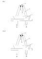
- terminals (2a and 2b) and electrically conductive supports 3 are attached to an insulator 1, at the ends thereof, the support 3 sandwich a tip 4 for emitting electrons and heaters 5 in the form of rectangular solids positioned at both side surfaces of the tip 4, and thereby hold the tip 4 and heaters 5.
- LaB 6 or the like can be used as the material of the electron emitting source tip 4.
- the heater may be an element of a carbonaceous material such as so-called hot press carbon (see Patent Document 1) which is obtained by hot-pressing a furan resin or the like, or a thermolytic carbon (see Patent Document 2).
- the above elements have anisotropic volume resistivity, and are usually shaped in the form of a rectangular solid, which is sandwiched by the electrically conductive supports 3 such as to allow passage of electricity in the direction of high volume resistivity.
- Patent Document 1 JP-B S60-23456
- Patent Document 2 JP-A S45-13831
- the tip 4 can be heated to a predetermined temperature by the heaters 5, and by further placing the tip 4 in an electric field, electrons can be extracted from the tip 4, enabling it to be used as an electron emitting source in electron beam lithography apparatus or electron microscopes.
- electron emitting sources are usually used by heating them, but when using a rare earth hexaboride such as LaB 6 as the electron emitting tip 4 and using a carbonaceous element as the heater, the resistance between the terminals (2a and 2b) can rise considerably depending on the storage time and conditions before use, as a result of which they can become impossible to electrically heat at the time of use. The reason for this seems to be that an insulating substance is formed as a product of hydrolysis of the electron emitting source tip 4 between the tip 4 and the heater 5.
- the purpose of the present invention is to suppress increases in inter-terminal resistance as described above, to offer a stable and electrically heatable charged particle source.
- the electron emitting source of the present invention is an electron emitting source comprising an electron emitting source tip composed of a rare earth hexaboride; and a heater composed of a carbonaceous member for holding and heating the electron emitting source tip, characterized in that an electrically conductive substance is provided between the electron emitting source tip and the heater.
- an electrically conductive substance is provided between the electron emitting source tip and the heater composed of a carbonaceous member, thereby suppressing reaction products generated by hydrolysis between the electron emitting source tip and the moisture in the gaseous phase, and preventing the increases in inter-terminal resistance occurring in conventionally known electron emitting sources.
- the electron emitting source of the present invention is capable of preventing the increases in inter-terminal resistance occurring in conventionally known electron emitting sources.
- FIG.1 A schematic view of a conventionally known electron emitting source.
- the present inventors performed various analyses in view of the situation in the conventional art, as a result of which they discovered that the above problems can be solved by, between the hexaboride and the heater composed of a carbonaceous member, covering the surface on the electron emitting source tip side with an electrically conductive substance, thereby resulting in the present invention.
- a carbon paste 6 is applied so as to fill the gap between the electron emitting source tip 4 and the heater 5.
- Colloidal graphite aqueous colloidal graphite was chosen for use as this carbon paste 6.
- the electron emitting source of the present invention as shown in Fig. 2 , it is preferable to use a carbon paste as the main component of the substance for filling the gap, since it is easy to apply to the surface of the electron emitting source tip.
- a carbon paste as the main component of the substance for filling the gap, since it is easy to apply to the surface of the electron emitting source tip.
- the substance there are no limitations on the substance, as long as the substance is not susceptible to reactions with an electron emitting source tip composed of a rare earth hexaboride and is capable of filling the gap between the electron emitting source tip and the heater 5.
- the portions of contact between the electron emitting source tip 4 composed of a rare earth hexaboride such as LaB 6 and the gaseous phase can be eliminated, thereby suppressing the generation of reaction products at the boundary between the electron emitting source tip 4 and the heater 5 as seen in conventional electron emitting sources.
- a rhenium layer 7 is provided between the electron emitting source tip 4 and the heater 5.
- the example of the electron emitting source of the present invention shown in Fig. 3 has a rhenium layer 7 in the form of a foil on the surface of the electron emitting tip 4 side.
- the electrically conductive substance may be in the form of a foil as long as the substance is not susceptible to reactions with the electron emitting source tip and the surface of the electron emitting source tip 4 side of the gap between the electron emitting source tip 4 and the heater 5 is isolated from the gaseous phase.
- the rhenium layer 7 is in the shape of a square U (or a U-shaped trough). However, it is not limited to this structure, as long as the surface on the electron emitting source tip 4 side of the gap between the electron emitting source tip 4 and the heater 5 is covered by the rhenium layer 7.
- the thickness of the rhenium layer 7 should be from 5 microns to 0.1 mm or less, due to spatial restrictions and power consumption when heating the electron emitting source tip 4.
- the portions of contact between the electron emitting source tip 4 composed of a rare earth hexaboride such as LaB 6 and the gaseous phase can be eliminated, thereby suppressing the generation of reaction products at the boundary between the electron emitting source tip 4 and the heater 5 as seen in conventional electron emitting sources.
- the electron emitting sources of Embodiments 1 and 2 are electron emitting sources comprising an electron emitting source tip 4 composed of a rare earth hexaboride and a heater 5 composed of a carbonaceous member for holding and heating the electron emitting source tip 4, wherein an electrically conductive substance (reference number 6 in Fig. 2 and reference number 7 in Fig. 3 ) is provided in the gap between the electron emitting tip source 4 and the heater 5.
- an electrically conductive substance reference number 6 in Fig. 2 and reference number 7 in Fig. 3
- the above-described electron emitting source can prevent increases in inter-terminal resistance which occur in conventionally known electron emitting sources.
- the electrically conductive substance may be an electrically conductive substance comprising one or more substances chosen from the group consisting of carbon, boron carbide and zirconium boride. This enables the electron emitting source to be obtained at low cost.
- the main component of the electrically conductive substance may be carbon. As a result, an electron emitting source of stable quality can be obtained.
- the electrically conductive substance may be an electrically conductive substance containing rhenium. As a result, an electron emitting source that suppresses increases in inter-terminal resistance can be obtained.
- the electron emitting sources of Embodiments 1 and 2 can be obtained by a method of manufacturing an electron emitting source comprising an electron emitting source tip 4 composed of a rare earth hexaboride and a heater composed of a carbonaceous member for holding and heating the electron emitting source tip 4, the method of manufacturing an electron emitting source being characterized by comprising a step of providing an electrically conductive substance in the gap between the electron emitting source tip 4 and the heater 5.
- the step of providing an electrically conductive substance in the gap between the electron emitting source tip 4 and the heater 5 may include a step of applying a carbon paste to the surface of the electron emitting source tip 4. Due to this manufacturing method, an electron emitting source of stable quality can be obtained at a lower cost.
- LaB 6 monocrystals were cut in the form of a rectangular column with dimensions of 0.6 mm ⁇ 0.75 mm ⁇ 2 mm, with the longest direction aligned with the ⁇ 100> crystal orientation, and one end with a 0.6 mm ⁇ 0.75 mm surface was shaped into a 90° cone, with the vertex of the cone being shaped into a sphere having a radius of 15 microns.
- thermolytic carbon was cut out to a size of 0.75 mm ⁇ 0.75 mm ⁇ 0.68 mm.
- Example 1 a carbon paste 6 (Oukenshoji Co., Ltd; product name "Colloidal Graphite”) was applied to the electron emitting source tip 4 as shown in Fig. 2 .
- the area of application of the carbon paste 6 was at least about the same as the contact area of the heaters 5.
- the terminals (2a and 2b) and the electrically conductive supports 3 were attached to the insulator 1, an electron emitting source tip 4 to which a carbon paste 6 has been applied and heaters 5 were sandwiched between the ends of the supports 3, so as to hold the electron emitting tip 4 and heaters 5, thereby resulting in an electron emitting source.
- Example 2 as shown in Fig. 3 , a rhenium foil (product of The Nilaco Corporation) with a thickness of 25 microns and a width of 0.75 mm was folded into the shape of a square U, and placed between the electron emitting source tip 4 and the heaters 5 positioned on the side surfaces thereof. Then, the terminals (2a and 2b) and the electrically conductive supports 3 were attached to the insulator 1, an electron emitting source tip 4 intermediated by a rhenium foil 7 and heaters 5 were sandwiched between the ends of the supports 3, so as to hold the electron emitting tip 4 and heaters 5, thereby resulting in an electron emitting source.
- a rhenium foil product of The Nilaco Corporation
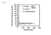
- the inter-terminal resistances at room temperature of the electron emitting sources according to Examples 1, 2 and the Comparative Example were measured with a tester (product of Hioki E. E. Corporation) having a measurement precision of 0.01 ohms, then they were placed in an isothermic isobaric tank set to a temperature of 80 °C and a high humidity of 80% relative humidity in order to accelerate the insulation forming reaction.
- the electron emitting sources of the examples and the comparative example were extracted from the isothermic isobaric tank after the passage of some time, to measure the inter-terminal resistance. This operation was repeated.
- the rate of increase after about 500 hours was less than 30%.
- the rate of increase suddenly increased, reaching more than 200%.
- the electron emitting source of the present invention is such that the inter-terminal resistance is not susceptible to increases even in high-temperature, high-humidity environments.
- the electron emitting source of the present invention has the effect of being capable of suppressing increases in inter-terminal resistance that occur depending on the storage time and conditions before use, thus being effective in improving the quality of electron emitting sources, which is extremely useful to industry.
Landscapes
- Chemical & Material Sciences (AREA)
- Analytical Chemistry (AREA)
- Electron Sources, Ion Sources (AREA)
- Solid Thermionic Cathode (AREA)
- Cold Cathode And The Manufacture (AREA)
Abstract
Description
- The present invention relates to an electron emitting source such as a thermionic cathode using lanthanum hexaboride or cerium hexaboride monocrystals used in electron microscopes, critical dimension scanning electron microscopes and electron beam exposure apparatus, and a method of manufacturing such an electron emitting source.
- An example of an electron emitting source used in equipment applying electron beams such as electron beam lithography apparatus and electron microscopes is one using an element functioning as an electrically heatable heater of highly crystalline carbon or the like, an electron emitting source tip (hereinafter referred to simply as a "tip") composed of a rare earth hexaboride that radiates electrons sandwiched by the aforementioned heater, and an electrically conductive support holding the aforementioned tip together with the heater (see Patent Document 1).
- More specifically, as shown for example in
Fig. 1 , terminals (2a and 2b) and electricallyconductive supports 3 are attached to aninsulator 1, at the ends thereof, thesupport 3 sandwich atip 4 for emitting electrons andheaters 5 in the form of rectangular solids positioned at both side surfaces of thetip 4, and thereby hold thetip 4 andheaters 5. LaB6 or the like can be used as the material of the electronemitting source tip 4. - The heater may be an element of a carbonaceous material such as so-called hot press carbon (see Patent Document 1) which is obtained by hot-pressing a furan resin or the like, or a thermolytic carbon (see Patent Document 2). The above elements have anisotropic volume resistivity, and are usually shaped in the form of a rectangular solid, which is sandwiched by the electrically
conductive supports 3 such as to allow passage of electricity in the direction of high volume resistivity.
Patent Document 1:JP-B S60-23456
Patent Document 2:JP-A S45-13831 - With the electron emitting source shown in
Fig.1 , by passing a DC current through the terminals (2a and 2b) in a high vacuum, thetip 4 can be heated to a predetermined temperature by theheaters 5, and by further placing thetip 4 in an electric field, electrons can be extracted from thetip 4, enabling it to be used as an electron emitting source in electron beam lithography apparatus or electron microscopes. - Normally, when using LaB6 or the like as the electron
emitting source tip 4, it is heated to 1400-1500 °C. - As described above, electron emitting sources are usually used by heating them, but when using a rare earth hexaboride such as LaB6 as the
electron emitting tip 4 and using a carbonaceous element as the heater, the resistance between the terminals (2a and 2b) can rise considerably depending on the storage time and conditions before use, as a result of which they can become impossible to electrically heat at the time of use. The reason for this seems to be that an insulating substance is formed as a product of hydrolysis of the electronemitting source tip 4 between thetip 4 and theheater 5. - The purpose of the present invention is to suppress increases in inter-terminal resistance as described above, to offer a stable and electrically heatable charged particle source.
- The electron emitting source of the present invention is an electron emitting source comprising an electron emitting source tip composed of a rare earth hexaboride; and a heater composed of a carbonaceous member for holding and heating the electron emitting source tip, characterized in that an electrically conductive substance is provided between the electron emitting source tip and the heater.
- With the electron emitting source having the above-described structure, an electrically conductive substance is provided between the electron emitting source tip and the heater composed of a carbonaceous member, thereby suppressing reaction products generated by hydrolysis between the electron emitting source tip and the moisture in the gaseous phase, and preventing the increases in inter-terminal resistance occurring in conventionally known electron emitting sources.
- The electron emitting source of the present invention is capable of preventing the increases in inter-terminal resistance occurring in conventionally known electron emitting sources.
- [
Fig.1 ] A schematic view of a conventionally known electron emitting source. - [
Fig. 2 ] A schematic view of an electron emitting source according toEmbodiment 1 of the present invention. - [
Fig. 3 ] A schematic view of an electron emitting source according toEmbodiment 2 of the present invention. - [
Fig. 4 ] A diagram showing the change in increase in inter-terminal resistance over elapsed time forEmbodiment 1,Embodiment 2 and a Comparative Example. -
- 1
- insulator
- 2a, 2b
- terminal
- 3
- electrically conductive support
- 4
- electron emitting source tip
- 5
- heater
- 6
- carbon paste
- 7
- rhenium layer
- The present inventors performed various analyses in view of the situation in the conventional art, as a result of which they discovered that the above problems can be solved by, between the hexaboride and the heater composed of a carbonaceous member, covering the surface on the electron emitting source tip side with an electrically conductive substance, thereby resulting in the present invention.
- Herebelow, examples of the present invention shall be explained with reference to
Fig. 2 and Fig. 3 , asEmbodiment 1 andEmbodiment 2. - In the example of the present invention shown in
Fig. 2 , acarbon paste 6 is applied so as to fill the gap between the electronemitting source tip 4 and theheater 5. Colloidal graphite (aqueous colloidal graphite) was chosen for use as thiscarbon paste 6. - By using such a electrically conductive paste, it can be easily applied to the surface of the electron emitting source tip.
- In the electron emitting source of the present invention as shown in
Fig. 2 , it is preferable to use a carbon paste as the main component of the substance for filling the gap, since it is easy to apply to the surface of the electron emitting source tip. However, there are no limitations on the substance, as long as the substance is not susceptible to reactions with an electron emitting source tip composed of a rare earth hexaboride and is capable of filling the gap between the electron emitting source tip and theheater 5. - Due to the above structure, the portions of contact between the electron
emitting source tip 4 composed of a rare earth hexaboride such as LaB6 and the gaseous phase can be eliminated, thereby suppressing the generation of reaction products at the boundary between the electronemitting source tip 4 and theheater 5 as seen in conventional electron emitting sources. - As substances that can be used aside from carbon, there are high melting point metals such as rhenium, as well as boron carbide, zirconium boride and the like, which are desirable for being boron compounds like LaB6.
- In the example of the present invention shown in
Fig. 3 , arhenium layer 7 is provided between the electronemitting source tip 4 and theheater 5. - The example of the electron emitting source of the present invention shown in
Fig. 3 has arhenium layer 7 in the form of a foil on the surface of theelectron emitting tip 4 side. In other words, the electrically conductive substance may be in the form of a foil as long as the substance is not susceptible to reactions with the electron emitting source tip and the surface of the electronemitting source tip 4 side of the gap between the electronemitting source tip 4 and theheater 5 is isolated from the gaseous phase. - As shown in
Fig. 3 , in the electron emitting source of the present invention, therhenium layer 7 is in the shape of a square U (or a U-shaped trough). However, it is not limited to this structure, as long as the surface on the electronemitting source tip 4 side of the gap between the electronemitting source tip 4 and theheater 5 is covered by therhenium layer 7. - The thickness of the
rhenium layer 7 should be from 5 microns to 0.1 mm or less, due to spatial restrictions and power consumption when heating the electronemitting source tip 4. - Due to the above structure, the portions of contact between the electron
emitting source tip 4 composed of a rare earth hexaboride such as LaB6 and the gaseous phase can be eliminated, thereby suppressing the generation of reaction products at the boundary between the electronemitting source tip 4 and theheater 5 as seen in conventional electron emitting sources. - Herebelow, the functions and effects of the electron emitting sources according to the above-described
Embodiments - The electron emitting sources of
Embodiments emitting source tip 4 composed of a rare earth hexaboride and aheater 5 composed of a carbonaceous member for holding and heating the electronemitting source tip 4, wherein an electrically conductive substance (reference number 6 inFig. 2 andreference number 7 inFig. 3 ) is provided in the gap between the electron emittingtip source 4 and theheater 5. - The above-described electron emitting source can prevent increases in inter-terminal resistance which occur in conventionally known electron emitting sources.
- The electrically conductive substance may be an electrically conductive substance comprising one or more substances chosen from the group consisting of carbon, boron carbide and zirconium boride. This enables the electron emitting source to be obtained at low cost.
- Additionally, the main component of the electrically conductive substance may be carbon. As a result, an electron emitting source of stable quality can be obtained.
- Additionally, the electrically conductive substance may be an electrically conductive substance containing rhenium. As a result, an electron emitting source that suppresses increases in inter-terminal resistance can be obtained.
- The electron emitting sources of
Embodiments source tip 4 composed of a rare earth hexaboride and a heater composed of a carbonaceous member for holding and heating the electron emittingsource tip 4, the method of manufacturing an electron emitting source being characterized by comprising a step of providing an electrically conductive substance in the gap between the electron emittingsource tip 4 and theheater 5. - Due to this manufacturing method, it is possible to obtain an electron emitting source capable of preventing increases in inter-terminal resistance.
- The step of providing an electrically conductive substance in the gap between the electron emitting
source tip 4 and theheater 5 may include a step of applying a carbon paste to the surface of the electron emittingsource tip 4. Due to this manufacturing method, an electron emitting source of stable quality can be obtained at a lower cost. - While the electron emitting source and electron emitting source manufacturing method of the present invention were explained by providing the examples of
Embodiment 1 andEmbodiment 2, the present invention is not limited to the above. Examples - Herebelow, the electron emitting source and electron emitting source manufacturing method of the present invention shall be explained in further detail by providing working examples and comparative examples, but these are not to be construed as limiting the present invention.
- First, as the material of the
electron emitting tip 4, LaB6 monocrystals were cut in the form of a rectangular column with dimensions of 0.6 mm × 0.75 mm × 2 mm, with the longest direction aligned with the <100> crystal orientation, and one end with a 0.6 mm × 0.75 mm surface was shaped into a 90° cone, with the vertex of the cone being shaped into a sphere having a radius of 15 microns. - Additionally, as the
heater 5, a thermolytic carbon was cut out to a size of 0.75 mm × 0.75 mm × 0.68 mm. - Additionally, in Example 1, a carbon paste 6 (Oukenshoji Co., Ltd; product name "Colloidal Graphite") was applied to the electron emitting
source tip 4 as shown inFig. 2 . In this case, the area of application of thecarbon paste 6 was at least about the same as the contact area of theheaters 5. Then, the terminals (2a and 2b) and the electricallyconductive supports 3 were attached to theinsulator 1, an electron emittingsource tip 4 to which acarbon paste 6 has been applied andheaters 5 were sandwiched between the ends of thesupports 3, so as to hold theelectron emitting tip 4 andheaters 5, thereby resulting in an electron emitting source. - In Example 2, as shown in
Fig. 3 , a rhenium foil (product of The Nilaco Corporation) with a thickness of 25 microns and a width of 0.75 mm was folded into the shape of a square U, and placed between the electron emittingsource tip 4 and theheaters 5 positioned on the side surfaces thereof. Then, the terminals (2a and 2b) and the electricallyconductive supports 3 were attached to theinsulator 1, an electron emittingsource tip 4 intermediated by arhenium foil 7 andheaters 5 were sandwiched between the ends of thesupports 3, so as to hold theelectron emitting tip 4 andheaters 5, thereby resulting in an electron emitting source. - In the Comparative Example, as shown in
Fig. 1 , the terminals (2a and 2b) and the electricallyconductive supports 3 were attached to theinsulator 1, an electron emittingsource tip 4 andheaters 5 in the form of rectangular solids provided on both side surfaces of thetip 4 were sandwiched between the ends of thesupports 3, so as to hold theelectron emitting tip 4 andheaters 5, thereby resulting in an electron emitting source. - The inter-terminal resistances at room temperature of the electron emitting sources according to Examples 1, 2 and the Comparative Example were measured with a tester (product of Hioki E. E. Corporation) having a measurement precision of 0.01 ohms, then they were placed in an isothermic isobaric tank set to a temperature of 80 °C and a high humidity of 80% relative humidity in order to accelerate the insulation forming reaction.
- After placement in the isothermic isobaric tank, the electron emitting sources of the examples and the comparative example were extracted from the isothermic isobaric tank after the passage of some time, to measure the inter-terminal resistance. This operation was repeated.
- Then, the rate of increase in inter-terminal resistance with the elapsed time was determined using the inter-terminal resistance before placement in the isothermic isobaric tank as a standard. The results of computation of this rate of increase are shown in
Fig. 4 . - As shown in
Fig. 4 , with the electron emitting sources of Examples 1 and 2, the rate of increase after about 500 hours was less than 30%. On the other hand, with the electron emitting sources, the rate of increase suddenly increased, reaching more than 200%. - Thus, the electron emitting source of the present invention is such that the inter-terminal resistance is not susceptible to increases even in high-temperature, high-humidity environments.
- The electron emitting source of the present invention has the effect of being capable of suppressing increases in inter-terminal resistance that occur depending on the storage time and conditions before use, thus being effective in improving the quality of electron emitting sources, which is extremely useful to industry.
Claims (6)
- An electron emitting source comprising an electron emitting source tip composed of a rare earth hexaboride; and a heater composed of a carbonaceous member for holding and heating said electron emitting source tip, characterized in that an electrically conductive substance is provided in a gap between said electron emitting source tip and the heater.
- An electron emitting source in accordance with claim 1, wherein said electrically conductive substance is an electrically conductive substance comprising at least one substance chosen from the group consisting of carbon, boron carbide and zirconium boride.
- An electron emitting source in accordance with claim 2, wherein the main component of said electrically conductive substance is carbon.
- An electron emitting source in accordance with claim 1, wherein said electrically conductive substance is an electrically conductive substance comprising rhenium.
- A method of manufacturing an electron emitting source comprising an electron emitting source tip composed of a rare earth hexaboride and a heater composed of a carbonaceous member for holding and heating said electron emitting source tip, the method of manufacturing an electron emitting source being characterized by comprising a step of providing an electrically conductive substance in a gap between said electron emitting source tip and the heater.
- A method of manufacturing an electron emitting source in accordance with claim 5, wherein the step of providing an electrically conductive substance in the gap between said electron emitting source tip and the heater comprises a step of applying a carbon paste to the surface of said electron emitting source tip.
Applications Claiming Priority (2)
| Application Number | Priority Date | Filing Date | Title |
|---|---|---|---|
| JP2007309726A JP4951477B2 (en) | 2006-12-04 | 2007-11-30 | Electron emission source |
| PCT/JP2008/062590 WO2009069335A1 (en) | 2007-11-30 | 2008-07-11 | Electron emitting source and manufacturing method of electron emitting source |
Publications (2)
| Publication Number | Publication Date |
|---|---|
| EP2216797A1 true EP2216797A1 (en) | 2010-08-11 |
| EP2216797A4 EP2216797A4 (en) | 2012-01-04 |
Family
ID=39695423
Family Applications (1)
| Application Number | Title | Priority Date | Filing Date |
|---|---|---|---|
| EP08778105A Withdrawn EP2216797A4 (en) | 2007-11-30 | 2008-07-11 | ELECTRON EMITTING SOURCE AND METHOD FOR MANUFACTURING ELECTRON EMITTING SOURCE |
Country Status (4)
| Country | Link |
|---|---|
| US (1) | US8456076B2 (en) |
| EP (1) | EP2216797A4 (en) |
| JP (1) | JP4951477B2 (en) |
| WO (1) | WO2009069335A1 (en) |
Families Citing this family (15)
| Publication number | Priority date | Publication date | Assignee | Title |
|---|---|---|---|---|
| JP5586013B2 (en) * | 2009-06-01 | 2014-09-10 | 独立行政法人物質・材料研究機構 | Refractory electron emission source |
| US8581481B1 (en) | 2011-02-25 | 2013-11-12 | Applied Physics Technologies, Inc. | Pre-aligned thermionic emission assembly |
| JP6043476B2 (en) * | 2011-10-12 | 2016-12-14 | 株式会社日立ハイテクノロジーズ | Ion source and ion beam apparatus using the same |
| US9165737B2 (en) * | 2012-10-04 | 2015-10-20 | Nuflare Technology, Inc. | High-brightness, long life thermionic cathode and methods of its fabrication |
| JP2014102929A (en) * | 2012-11-19 | 2014-06-05 | Nuflare Technology Inc | Cathode and method for manufacturing cathode |
| JP6529920B2 (en) * | 2016-03-01 | 2019-06-12 | 株式会社日立ハイテクノロジーズ | Field emission electron source, method of manufacturing the same, and electron beam apparatus |
| JP6938498B2 (en) * | 2016-07-19 | 2021-09-22 | デンカ株式会社 | Electron source and its manufacturing method |
| JP2019153563A (en) * | 2018-03-06 | 2019-09-12 | 株式会社Param | Electron gun |
| JP6548179B1 (en) * | 2018-03-19 | 2019-07-24 | 株式会社Param | Electron gun |
| US11380511B2 (en) * | 2020-03-24 | 2022-07-05 | Fei Company | Charged particle beam source |
| US20230298846A1 (en) * | 2020-08-17 | 2023-09-21 | Denka Company Limited | Emitter and device provided with same |
| JP7680935B2 (en) * | 2021-10-26 | 2025-05-21 | 株式会社ニューフレアテクノロジー | Electron gun cathode mechanism and method for manufacturing the same |
| CN118922907A (en) | 2022-03-29 | 2024-11-08 | 电化株式会社 | Transmitter and device provided with same |
| JP2025536684A (en) | 2022-11-16 | 2025-11-07 | キンボール・フィジックス・インコーポレーテッド | Pincer Mount Cathode |
| JP2025144131A (en) * | 2024-03-19 | 2025-10-02 | デンカ株式会社 | Electron source, manufacturing method thereof, and electron beam device |
Family Cites Families (30)
| Publication number | Priority date | Publication date | Assignee | Title |
|---|---|---|---|---|
| US3312856A (en) * | 1963-03-26 | 1967-04-04 | Gen Electric | Rhenium supported metallic boride cathode emitters |
| JPS4513831Y1 (en) | 1965-04-14 | 1970-06-12 | ||
| US3532923A (en) * | 1969-03-17 | 1970-10-06 | Ibm | Pyrolytic graphite support for lanthanum hexaboride cathode emitter |
| NL167796C (en) * | 1972-05-30 | 1982-01-18 | Philips Nv | METHOD FOR MANUFACTURING A LANTHANE HEXABORIDE-ACTIVATED CATHOD FOR AN ELECTRIC DISCHARGE TUBE |
| JPS6023456B2 (en) * | 1978-11-01 | 1985-06-07 | 電気化学工業株式会社 | Thermionic cathode device |
| JPS5618335A (en) * | 1979-07-20 | 1981-02-21 | Jeol Ltd | Electron gun |
| JPS5763744A (en) * | 1980-10-02 | 1982-04-17 | Fujitsu Ltd | Electron gun |
| JPS57196443A (en) * | 1981-05-29 | 1982-12-02 | Denki Kagaku Kogyo Kk | Manufacture of hot cathode |
| US4528474A (en) * | 1982-03-05 | 1985-07-09 | Kim Jason J | Method and apparatus for producing an electron beam from a thermionic cathode |
| US4760306A (en) * | 1983-06-10 | 1988-07-26 | The United States Of America As Represented By The United States Department Of Energy | Electron emitting filaments for electron discharge devices |
| JPS6023456A (en) | 1983-07-18 | 1985-02-06 | Tetsuhiko Inoue | Non-toxic mildew-proofing paint |
| JPS62140331A (en) * | 1985-12-16 | 1987-06-23 | Hitachi Ltd | thermionic emission cathode |
| JPH0810578B2 (en) | 1986-06-23 | 1996-01-31 | 株式会社日立製作所 | Lanthanum hexaboride hot cathode |
| GB2192751B (en) * | 1986-07-14 | 1991-02-13 | Denki Kagaku Kogyo Kk | Method of making a thermionic cathode structure. |
| CH672860A5 (en) * | 1986-09-29 | 1989-12-29 | Balzers Hochvakuum | |
| NL8800539A (en) * | 1988-03-03 | 1989-10-02 | Philips Nv | ELECTRON BUNDLE DEVICE. |
| JPH01154424A (en) * | 1988-10-25 | 1989-06-16 | Denki Kagaku Kogyo Kk | Thermionic emission cathode |
| EP0417340A1 (en) | 1989-09-12 | 1991-03-20 | Siemens Aktiengesellschaft | Electron source |
| JPH0676730A (en) | 1992-08-24 | 1994-03-18 | Denki Kagaku Kogyo Kk | Thermonic emission cathode |
| JPH06231708A (en) * | 1993-02-04 | 1994-08-19 | Mitsubishi Heavy Ind Ltd | Long electron beam generator |
| JPH0737484A (en) * | 1993-07-23 | 1995-02-07 | Denki Kagaku Kogyo Kk | Thermionic radiation negative electrode |
| JPH07335161A (en) * | 1994-06-03 | 1995-12-22 | Hitachi Medical Corp | Electron gun |
| US5988014A (en) | 1996-06-21 | 1999-11-23 | Trw Automotive Safety Systems Gmbh | Sheet-metal steering wheel |
| JP2000058448A (en) * | 1998-06-05 | 2000-02-25 | Nikon Corp | Electron beam transfer apparatus and semiconductor device manufacturing method |
| DE20005531U1 (en) * | 2000-03-29 | 2000-06-21 | Patent-Treuhand-Gesellschaft für elektrische Glühlampen mbH, 81543 München | Short arc lamp |
| JP2001325910A (en) * | 2000-05-16 | 2001-11-22 | Denki Kagaku Kogyo Kk | Electron gun and how to use it |
| JP4648527B2 (en) * | 2000-08-31 | 2011-03-09 | 新日本無線株式会社 | Method for manufacturing cathode |
| JP2005190758A (en) * | 2003-12-25 | 2005-07-14 | Denki Kagaku Kogyo Kk | Electron source |
| JP4725911B2 (en) | 2005-08-04 | 2011-07-13 | タカタ株式会社 | Seat belt retractor and seat belt device provided with the same |
| JP5065903B2 (en) * | 2005-11-08 | 2012-11-07 | 株式会社アドバンテスト | Exposure method |
-
2007
- 2007-11-30 JP JP2007309726A patent/JP4951477B2/en not_active Expired - Fee Related
-
2008
- 2008-07-11 WO PCT/JP2008/062590 patent/WO2009069335A1/en not_active Ceased
- 2008-07-11 EP EP08778105A patent/EP2216797A4/en not_active Withdrawn
- 2008-07-11 US US12/745,316 patent/US8456076B2/en not_active Expired - Fee Related
Also Published As
| Publication number | Publication date |
|---|---|
| WO2009069335A1 (en) | 2009-06-04 |
| JP4951477B2 (en) | 2012-06-13 |
| US20100301736A1 (en) | 2010-12-02 |
| EP2216797A4 (en) | 2012-01-04 |
| US8456076B2 (en) | 2013-06-04 |
| JP2008166265A (en) | 2008-07-17 |
Similar Documents
| Publication | Publication Date | Title |
|---|---|---|
| US8456076B2 (en) | Electron emitting source and manufacturing method of electron emitting source | |
| JP5117146B2 (en) | Heating device | |
| EP2833396B1 (en) | Flow channel member, heat exchanger provided with flow channel member, and semiconductor manufacturing apparatus provided with flow channel member | |
| US5997998A (en) | Resistance element | |
| TWI768045B (en) | Magnesium-based thermoelectric conversion material, magnesium-based thermoelectric conversion element, and method for producing magnesium-based thermoelectric conversion material | |
| US20200154524A1 (en) | Electrical resistor, honeycomb structure and electrically heated catalyst device | |
| CN110352182B (en) | Heater for semiconductor manufacturing device | |
| JP6798640B2 (en) | Manufacturing method of electrostatic chuck device and electrostatic chuck device | |
| JP5780620B2 (en) | PTC thermistor member | |
| EP3767689A1 (en) | Thermoelectric conversion element | |
| US12284918B2 (en) | Thermoelectric conversion element, thermoelectric conversion module, and method of producing thermoelectric conversion element | |
| EP4191636B1 (en) | Electron emitter | |
| JPH0676730A (en) | Thermonic emission cathode | |
| JPH09245946A (en) | Ceramic heater | |
| JP5047062B2 (en) | Thermionic emission cathode | |
| JP2014099431A (en) | Composite ptc thermistor member | |
| Itou et al. | Collapse of the charge order in (DI-DCNQI) 2 Ag by dimensional crossover | |
| TW201338633A (en) | Microwave heating device and microwave heating method | |
| EP2862224B1 (en) | Fuel cell component with embedded power connector | |
| KR20100111627A (en) | Electrostatic chuck | |
| JP7590543B2 (en) | heater | |
| JP2010015815A (en) | Cathode structure for electron tube | |
| JP2006012496A (en) | Electron source | |
| KR20230148735A (en) | Power feeding part for electrostatic chuck, and electrostatic chuck | |
| Novokhatska et al. | Role of Excess Manganese in Formation of the Structure and Transport Properties of Manganite [([Nd. sub. 0.67][Sr. sub. 0.33]). sub. 1-x][Mn. sub. 1+ x][O. sub. 3](x= 0, 0.2) Sintered at 1273-1473 K |
Legal Events
| Date | Code | Title | Description |
|---|---|---|---|
| PUAI | Public reference made under article 153(3) epc to a published international application that has entered the european phase |
Free format text: ORIGINAL CODE: 0009012 |
|
| 17P | Request for examination filed |
Effective date: 20100528 |
|
| AK | Designated contracting states |
Kind code of ref document: A1 Designated state(s): AT BE BG CH CY CZ DE DK EE ES FI FR GB GR HR HU IE IS IT LI LT LU LV MC MT NL NO PL PT RO SE SI SK TR |
|
| AX | Request for extension of the european patent |
Extension state: AL BA MK RS |
|
| DAX | Request for extension of the european patent (deleted) | ||
| A4 | Supplementary search report drawn up and despatched |
Effective date: 20111206 |
|
| RIC1 | Information provided on ipc code assigned before grant |
Ipc: H01J 37/06 20060101ALI20111130BHEP Ipc: H01J 37/065 20060101ALI20111130BHEP Ipc: H01J 1/15 20060101AFI20111130BHEP |
|
| 17Q | First examination report despatched |
Effective date: 20140925 |
|
| RAP1 | Party data changed (applicant data changed or rights of an application transferred) |
Owner name: DENKA COMPANY LIMITED |
|
| STAA | Information on the status of an ep patent application or granted ep patent |
Free format text: STATUS: THE APPLICATION IS DEEMED TO BE WITHDRAWN |
|
| 18D | Application deemed to be withdrawn |
Effective date: 20160415 |