EP2211393A2 - Light emitting device - Google Patents
Light emitting device Download PDFInfo
- Publication number
- EP2211393A2 EP2211393A2 EP09014533A EP09014533A EP2211393A2 EP 2211393 A2 EP2211393 A2 EP 2211393A2 EP 09014533 A EP09014533 A EP 09014533A EP 09014533 A EP09014533 A EP 09014533A EP 2211393 A2 EP2211393 A2 EP 2211393A2
- Authority
- EP
- European Patent Office
- Prior art keywords
- layer
- light emitting
- emitting device
- conductive semiconductor
- semiconductor layer
- Prior art date
- Legal status (The legal status is an assumption and is not a legal conclusion. Google has not performed a legal analysis and makes no representation as to the accuracy of the status listed.)
- Granted
Links
Images


Classifications
-
- H—ELECTRICITY
- H10—SEMICONDUCTOR DEVICES; ELECTRIC SOLID-STATE DEVICES NOT OTHERWISE PROVIDED FOR
- H10H—INORGANIC LIGHT-EMITTING SEMICONDUCTOR DEVICES HAVING POTENTIAL BARRIERS
- H10H20/00—Individual inorganic light-emitting semiconductor devices having potential barriers, e.g. light-emitting diodes [LED]
- H10H20/80—Constructional details
- H10H20/83—Electrodes
- H10H20/831—Electrodes characterised by their shape
- H10H20/8312—Electrodes characterised by their shape extending at least partially through the bodies
-
- H—ELECTRICITY
- H10—SEMICONDUCTOR DEVICES; ELECTRIC SOLID-STATE DEVICES NOT OTHERWISE PROVIDED FOR
- H10H—INORGANIC LIGHT-EMITTING SEMICONDUCTOR DEVICES HAVING POTENTIAL BARRIERS
- H10H20/00—Individual inorganic light-emitting semiconductor devices having potential barriers, e.g. light-emitting diodes [LED]
- H10H20/80—Constructional details
- H10H20/872—Periodic patterns for optical field-shaping, e.g. photonic bandgap structures
Definitions
- the disclosure relates to a light emitting device for converting a current into light.
- a light emitting diode is a semiconductor light emitting device used to convert a current into light.
- the wavelength of light emitted from the LED depends on a semiconductor material used to manufacture the LED. This is because the wavelength of the emitted light depends on a band-gap of the semiconductor material representing an energy difference between electrons of a valence band and electrons of a conduction band.
- the brightness of the conventional LED has increased, so that the conventional LED has been employed as a light source for a display device, a vehicle, or an illumination device.
- the conventional LED can represent a white color having superior light efficiency by employing phosphors or combining LEDs having various colors.
- the brightness of the conventional LED is changed according to various conditions such as an active-layer structure, a light extraction structure for extracting light to the outside, a chip size, and the type of molding materials surrounding the LED.
- An embodiment of the invention provides a light emitting device employing an improved structure.
- the embodiment provides a light emitting device having improved light extraction efficiency.
- a light emitting device that includes a first photonic crystal structure including a reflective layer and non-metal pattern elements on the reflective layer, a second conductive semiconductor layer on both the reflective layer and the non-metal pattern elements, an active layer on the second conductive semiconductor layer, and a first conductive semiconductor layer on the active layer.
- a light emitting device that includes a reflective layer, a transparent electrode layer including protrusion pattern elements protruding in an arrangement direction of the reflective layer on the reflective layer, a second conductive semiconductor layer on the transparent electrode layer, an active layer on the second conductive semiconductor layer, and a first conductive semiconductor layer on the active layer.
- a light emitting device includes a first photonic crystal structure including a transparent electrode layer and reflective pattern elements on the transparent electrode layer, a second conductive semiconductor layer on both the transparent electrode layer and the reflective pattern elements, an active layer on the second conductive semiconductor layer, and a first conductive semiconductor layer on the active layer.
- each layer shown in the drawings can be exaggerated, omitted or schematically drawn for the purpose of convenience or clarity.
- the size of elements does not utterly reflect an actual size.
- FIG. 1 is a view showing a light emitting device according to a first embodiment.
- the light emitting device includes a second electrode layer 10, a reflective layer 20 formed on the second electrode layer 10, a non-metal pattern layer 80 formed on the reflective layer 20, a second conductive semiconductor layer 30 formed on both the non-metal pattern layer 80 and the reflective layer 20, an active layer 40 formed on the second conductive semiconductor layer 30, a first conductive semiconductor layer 50 formed on the active layer 40, and a first electrode layer 70 formed on the first conductive semiconductor layer 50.
- a non-conductive semiconductor layer 60 may be selectively formed on the first conductive semiconductor layer 50.
- the second electrode layer 10 may include at least one of copper (Cu), titanium (Ti), chromium (Cr), nickel (Ni), aluminum (Al), platinum (Pt), gold (Au), tungsten (W), and a semiconductor substrate doped with impurities.
- the second electrode layer 10 supplies power to the active layer 40 in cooperation with the first electrode layer 70.
- the reflective layer 20 may include at least one of silver (Ag), alloy including Ag, Al, and alloy including Al which have a high reflective index.
- an adhesion metal layer including nickel (Ni) or titanium (Ti) may be formed between the second electrode layer 10 and the reflective layer 20 such that an interfacial adhesion strength can be enhanced between the second electrode layer 10 and the reflective layer 20.
- the non-metal pattern layer 80 that is formed on the reflective layer 20 faces the second conductive semiconductor layer 30. At least a portion of a side surface of the non-metal pattern layer 80 may be surrounded by the reflective layer 20.
- the non-metal pattern layer 80 and the reflective layer 20 form a first photonic crystal structure 90.
- the non-metal pattern layer 80 includes a non-metal material, and has a refractive index greater than that of air and smaller than that of the second conductive semiconductor layer 30.
- the non-metal pattern layer 80 may be formed by patterning a non-metal layer after forming the non-metal layer on the second conductive semiconductor layer 30 in the manufacturing process of the light emitting device. Thereafter, the reflective layer 20 may be formed on the resultant structure. As shown in FIG. 1 , the light emitting device is formed with the second electrode layer 10, the reflective layer 20 is provided on a side surface or a lower surface of the non-metal pattern layer 80. In addition, the second electrode layer 10 is provided on a lower surface of the reflective layer 20.
- the non-metal pattern layer 80 may include a transparent electrode, for example, at least one of tin-doped indium oxide (ITO), zinc oxide (ZnO), gallium-doped zinc oxide (GZO), ruthenium oxide (RuO x ), and iron oxide (IrO x ).
- a transparent electrode for example, at least one of tin-doped indium oxide (ITO), zinc oxide (ZnO), gallium-doped zinc oxide (GZO), ruthenium oxide (RuO x ), and iron oxide (IrO x ).
- the non-metal pattern layer 80 may include a dielectric substance.
- the non-metal pattern layer 80 may include at least one of silicon oxide (SiO 2 ), magnesium fluoride (MgF 2 ), titanium dioxide (TiO 2 ), aluminum oxide (Al 2 O 3 ), spin on glass (SOG), and silicon nitride (Si 3 N 4 ).
- SiO 2 silicon oxide
- MgF 2 magnesium fluoride
- TiO 2 titanium dioxide
- Al 2 O 3 aluminum oxide
- SOG spin on glass
- Si 3 N 4 silicon nitride
- the reflective layer 20 may have pattern elements spaced apart from each other by a predetermined interval on the same horizontal plane as that of the non-metal pattern layer 80.
- an ohmic-contact layer can be formed between the reflective layer 20 and the second conductive semiconductor layer 30.
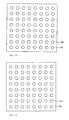
- FIGS. 12 and 13 are plan views showing the first photonic crystal structure 90.
- the non-metal pattern layer 80 may have pattern elements spaced apart from each other on the reflective layer 20.
- the reflective layer 20 may have pattern elements spaced apart from each other on the non-metal pattern layer 80.
- the reflective layer 20 and the non-metal pattern layer 80 that form the first photonic crystal structure 90 allow light to be effectively transmitted from the light emitting device.
- the light extraction efficiency of the first photonic crystal structure 90 can be determined according to a refractive index contrast.
- the non-metal pattern layer 80 is formed of using a transparent electrode or a dielectric substance
- the reflective layer 20 is formed of a metal mirror below or beside the non-metal pattern layer 80, a greater diffraction effect is generated as compared with the diffraction effect caused by the refractive index contrast.
- the second conductive semiconductor layer 30 may be formed as a GaN-based semiconductor layer doped with P-type impurities
- the first conductive semiconductor layer 50 may be formed as a GaN-based semiconductor layer doped with N-type impurities.
- the active layer 40 may have at least one of a single quantum well structure, a multi-quantum well structure, a quantum-wire structure, and a quantum dot structure.
- the non-conductive semiconductor layer 60 may be selectively formed, and has electrical conductivity significantly lower than those of the first conductive semiconductor layer 50 and the second conductive semiconductor layer 30.
- the non-conductive semiconductor layer 60 may be an un-doped GaN layer.
- the first electrode layer 70 is aligned perpendicularly to the second electrode layer 10 and the non-metal pattern layer 80, including a transparent electrode or a dielectric substance, is formed between the second conductive semiconductor layer 30 and the reflective layer 20, so that the first photonic crystal structure 90 (including the reflective layer 20 that is in contact with the lower surface and side surfaces of the non-metal pattern layer 80) can be obtained.
- the first photonic crystal structure 90 includes the non-metal pattern layer 80 formed of a transparent electrode or a dielectric substance and the reflective layer 20 includes metal having a refractive index represented in a complex number, such that a strong diffraction effect can be represented. Accordingly, the light extraction effect can be improved.
- FIG. 2 is a view showing a light emitting device according to a second embodiment.
- details identical to those of the first embodiment will be omitted in order to avoid redundancy.
- the light emitting device includes the second electrode layer 10, the reflective layer 20 formed on the second electrode layer 10, a transparent electrode layer 81 having a protrusion pattern layer 82 on the reflective layer 20, the second conductive semiconductor layer 30 formed on the transparent electrode layer 81, the active layer 40 formed on the second conductive semiconductor layer 30, the first conductive semiconductor layer 50 formed on the active layer 40, and the first electrode layer 70 formed on the first conductive semiconductor layer 50.
- the non-conductive semiconductor layer 60 may be selectively formed on the first conductive semiconductor layer 50.
- the protrusion pattern layer 82 of the transparent electrode layer 81 and the reflective layer 20 form the first photonic crystal structure 90.
- the protrusion pattern layer 82 protrudes towards the reflective layer 20.
- the protrusion pattern layer 82 may have pattern elements spaced apart from each other by a predetermined interval. In other words, lower surfaces and side surfaces of the pattern elements of the protrusion pattern layer 82 are surrounded by the reflective layer 20.
- the protrusion pattern layer 82 may be formed by selectively etching or depositing the transparent electrode layer 81 after forming the transparent electrode layer 81 on the second conductive semiconductor layer 30.
- the transparent electrode layer 81 may include at least one of ITO, ZnO, GZO, RuOx, and IrO x .
- the pattern elements of the protrusion pattern layer 82 are spaced apart from each other by a predetermined interval.
- the transparent electrode layer 81 may have a roughness on a surface facing the reflective layer 20.
- the first photonic crystal structure 90 includes the protrusion pattern layer 82 of the transparent electrode layer 81 and the reflective layer 20, which is formed as a metal mirror, in the contact with the protrusion pattern layer 82 so that a desirable diffraction effect can be represented.
- the light extraction efficiency of the light emitting device can be improved.
- FIG. 3 is a view showing a light emitting device according to a third embodiment.
- details identical to that of the first embodiment will be omitted in order to avoid redundancy.
- the light emitting device includes the second electrode layer 10, the reflective layer 20 formed on the second electrode layer 10, the second conductive semiconductor layer 30 including protrusion pattern layer 31 on the reflective layer 20, the active layer 40 formed on the second conductive semiconductor layer 30, the first conductive semiconductor layer 50 formed on the active layer 40, and the first electrode layer 70 formed on the first conductive semiconductor layer 50.
- the non-conductive semiconductor layer 60 may be selectively formed on the first conductive semiconductor layer 50.
- the protrusion pattern layer 31 of the second conductive semiconductor layer 30 and the reflective layer 20 form the first photonic crystal structure 90.
- the protrusion pattern layer 31 protrudes toward the reflective layer 20, and may have pattern elements spaced apart from each other by a predetermined interval. Lower surfaces and side surfaces of pattern elements of the protrusion pattern layer 31 are surrounded by the reflective layer 20.
- the protrusion pattern layer 31 may be formed by selectively etching the second conductive semiconductor layer 30 after forming the second conductive semiconductor layer 30 or by forming roughness on the surface of the second conductive semiconductor layer 30 through the adjustment of a growth condition of the second conductive semiconductor layer 30. Since the protrusion pattern layer 31 may include a GaN-based semiconductor layer, the protrusion pattern layer 31 may be one kind of a non-metal pattern layer.
- the pattern elements of the protrusion pattern layer 31 are spaced apart from each other by a predetermined interval.
- the second conductive semiconductor layer 30 may have a roughness at a surface facing the reflective layer 20.
- the first photonic crystal structure 90 includes the protrusion pattern layer 31 of the second conductive semiconductor layer 30, which is formed by using the GaN-based semiconductor layer, and the reflective layer 20, which is formed as a metal mirror, in contact with the protrusion pattern layer 31, so that a desirable diffraction effect can be represented.
- the light extraction efficiency of the light emitting device can be improved.
- FIG. 4 is a view showing a light emitting device according to a fourth embodiment.
- details identical to that of the first embodiment will be omitted in order to avoid redundancy.
- the light emitting device includes the second electrode layer 10, a reflective layer 22 formed on the second electrode layer 10, the transparent electrode layer 81 formed on the reflective layer 22, a reflective pattern layer 23 formed on the transparent electrode layer 81, the second conductive semiconductor layer 30 formed on both the transparent electrode layer 81 and the reflective pattern layer 23, the active layer 40 formed on the second conductive semiconductor layer 30, the first conductive semiconductor layer 50 formed on the active layer 40, and the first electrode layer 70 formed on the first conductive semiconductor layer 50.
- non-conductive semiconductor layer 60 may be selectively formed on the first conductive semiconductor layer 50.
- the transparent electrode layer 81 and the reflective pattern layer 23 form the first photonic crystal structure 90.
- the reflective pattern layer 23 may have pattern elements spaced apart from each other by a predetermined interval. In other words, lower surfaces and side surfaces of the pattern elements of the reflective pattern layer 23 are surrounded by the transparent electrode layer 81.
- the reflective pattern layer 23 may be formed by selectively etching or depositing a reflective material layer after forming the reflective material layer on the second conductive semiconductor layer 30.
- the transparent electrode layer 81 may include at least one of ITO, ZnO, GZO, RuO x , and IrO x .
- the first photonic crystal structure 90 includes the transparent electrode layer 81 and the reflective pattern layer 23, so that a desirable diffraction effect can be represented.
- the reflective layer 22 is provided under the transparent electrode layer 81 such that light generated from the active layer 40 can be reflected upward. If the second electrode layer 10 includes a material having high reflectivity, the reflective layer 22 can be omitted.
- the light extraction efficiency of the light emitting device can be improved.
- FIG. 5 is a view showing a light emitting device according to a fifth embodiment.
- details identical to that of the first embodiment will be omitted in order to avoid redundancy.
- the light emitting device includes the second electrode layer 10, the reflective layer 20 formed on the second electrode layer 10, the non-metal pattern layer 80 formed on the reflective layer 20, the second conductive semiconductor layer 30 formed on both the non-metal pattern layer 80 and the reflective layer 20, the active layer 40 formed on the second conductive semiconductor layer 30, the first conductive semiconductor layer 50 formed on the active layer 40, the first electrode layer 70 formed on the first conductive semiconductor layer 50, and the non-conductive semiconductor layer 60 formed on the first conductive semiconductor layer 50.
- a second photonic crystal structure 100 having a column shape or a hole shape is formed from the non-conductive semiconductor layer 60.
- the second photonic crystal structure 100 includes a patterned structure 61.
- the patterned structure may include holes or columns.
- the columns or holes 61 may be aligned with a predetermined interval or randomly. This improves the light extraction efficiency of the light emitting device.
- the second photonic crystal structure 100 is formed on the non-conductive semiconductor layer 60 according to the fifth embodiment, the second photonic crystal structure 100 is identically applicable to the second to fourth embodiments.
- the second photonic crystal structure 100 may be formed on the first conductive semiconductor layer 50 without the non-conductive semiconductor layer 60. This is identically applicable to the second to third embodiments.
- FIG. 6 is a view showing a simulation structure used to determine the effect of the first photonic crystal structure 90 in a light emitting device according to the embodiments.
- FIG. 7 is a graph showing extraction efficiency as a function of a propagation distance when the first photonic crystal structure 90 is formed in a light emitting device or not.
- a finite different time domain (FDTD) method is utilized to determine the light extraction effect of a first photonic crystal structure. It is assumed that a metal mirror 21 corresponding to the reflective layer includes Ag. A Drude model is employed to precisely depict Ag in a calculation space. ITO is used as a transparent metal for the transparent electrode layer 81. The thickness h of the transparent electrode layer 81 is assumed as 0.1 ⁇ m, and a lattice constant of the transparent electrode layer 81 is about 1 ⁇ m.
- the transparent electrode layer 81 has a refractive index of about 2.0
- a light emitting layer on the transparent electrode layer 81 is a GaN layer 121 having a refractive index of about 2.46
- an epoxy layer 110 having a refractive index of about 1.4 is provided on the GaN layer 121.
- the GaN layer 121 has a thickness of about 3 ⁇ m.
- a multi quantum well 41 is provided in the GaN layer 121.
- the light emitting device having the first photonic crystal structure when comparing a light emitting device employing the first photonic crystal structure with a light emitting device not employing the first photonic crystal structure, the light emitting device having the first photonic crystal structure more increases light extraction efficiency as a propagation distance of light is increased. In contrast, when the light emitting device does not employ the first photonic crystal structure, the light extraction efficiency is not increased after the propagation distance exceeds a predetermined value.
- the non-metal pattern layer 80 or the protrusion pattern layer 31 or 82 is not formed between the second conductive semiconductor layer 30 and the reflective layer 20.
- the light emitting device employing the first photonic crystal structure more increases the light extraction efficiency compared to the light emitting device not employing the first photonic crystal structure.
- FIG. 8 is a graph representing light extraction efficiency according to the lattice constant of the non-metal pattern layer 80 in the first photonic crystal structure of the light emitting device according to the embodiments.
- FIG. 8 is a graph showing a simulation when the non-metal pattern layer 80 has a refractive index of about 2.0, and includes an ITO layer having a pattern thickness of about 0.1 ⁇ m.
- the non-metal pattern layer 80 when the non-metal pattern layer 80 is formed with a lattice constant in the range of about ⁇ /n to about 10 ⁇ /n, the light extraction efficiency can be improved.
- ⁇ refers to the wavelength of light transmitted from the LED.
- blue light from the LED has the wavelength of about 470nm.
- n refers to a refractive index of a material forming a light emitting layer of the light emitting device.
- the refractive index is about 2.46.
- the non-metal pattern layer 80 is formed with a lattice constant in the range of about ⁇ /n to about 10 ⁇ /n, the light extraction efficiency is improved by more than 1.5 times that of the LED not employing the first photonic crystal structure.
- the light emitting device emits light of about 470nm and includes a GaN-based semiconductor layer having a refractive index of about 2.46.
- ⁇ /n is about 0.191 ⁇ m.
- the non-metal pattern layer 80 has a lattice constant about 0.2 ⁇ m, the maximum light extraction efficiency is represented.
- the light extraction efficiency can be improved when the lattice constant of the protrusion pattern layer 31 or 82 and the reflective pattern layer 23 is in the rang of ⁇ /n to about 10 ⁇ /n.
- FIG. 9 is a graph representing light extraction efficiency according to the pattern thickness of the non-metal pattern layer 80 in the first photonic crystal structure of the light emitting device according to the embodiments.
- FIG. 9 is a graph showing a simulation when the non-metal pattern layer 80 has a refractive index of about 2.0, and includes an ITO layer having lattice constants a of about 400nm and about 1200nm.
- the non-metal pattern layer 80 has a thickness in the range of about 10nm to 100nm regardless of the lattice constant of the non-metal pattern layer 80, the light extraction efficiency is improved by more than 1.8 times.
- the non-metal pattern layer 80 has a thickness of about 100nm or more, the light extraction efficiency is more improved compared to that of the light emitting device not employing the first photonic crystal structure.
- the pattern thickness of the non-metal pattern layer 80 need not exceed about 300nm or more.
- the protrusion pattern layer 31 or 82 has a lattice constant in the range of about 200nm to about 700nm and a thickness in the range of about 200nm to about 400nm, the light extraction efficiency of the LED according to the second and third embodiments is improved.
- the protrusion pattern layer 31 or 82 has a lattice constant in the range of about 700nm to about 2000nm and a thickness in the range of about 600nm to about 1200nm, the light extraction efficiency of the light emitting device according to the second and third embodiments is improved.
- FIG. 10 is a graph showing light extraction efficiency when the first photonic crystal structure, the second photonic crystal structure, and both the first and second photonic crystal structures are formed in the light emitting device.
- FIG. 11 is a graph showing light extraction efficiency according to the lattice constant of the non-metal pattern layer of the first photonic crystal structure and a lattice constant of columns or holes of the second photonic crystal structure in the light emitting device according to the embodiment.
- the light extraction efficiency is the maximum when the lattice constant of the non-metal pattern layer 80 forming the first photonic crystal structure is about 0.2 ⁇ m.
- the light extraction efficiency is the maximum when the lattice constant of columns or holes forming the second photonic crystal structure is about 0.6 ⁇ m.
- the lattice constant of the non-metal pattern layer 80 forming the first photonic crystal structure is in the rang of about 200nm to about 600nm, and the lattice constant of columns or holes 61 forming the second photonic crystal structure is in the range of about 600nm to about 1800nm, the light extraction efficiency is improved.
- the patterned structure 61 may be present with any of the previously described embodiments.
Landscapes
- Led Devices (AREA)
Abstract
Description
- The disclosure relates to a light emitting device for converting a current into light.
- A light emitting diode (LED) is a semiconductor light emitting device used to convert a current into light.
- The wavelength of light emitted from the LED depends on a semiconductor material used to manufacture the LED. This is because the wavelength of the emitted light depends on a band-gap of the semiconductor material representing an energy difference between electrons of a valence band and electrons of a conduction band.
- Recently, the brightness of the conventional LED has increased, so that the conventional LED has been employed as a light source for a display device, a vehicle, or an illumination device. In addition, the conventional LED can represent a white color having superior light efficiency by employing phosphors or combining LEDs having various colors.
- Meanwhile, the brightness of the conventional LED is changed according to various conditions such as an active-layer structure, a light extraction structure for extracting light to the outside, a chip size, and the type of molding materials surrounding the LED.
- An embodiment of the invention provides a light emitting device employing an improved structure.
- The embodiment provides a light emitting device having improved light extraction efficiency.
- According to one embodiment, there is a light emitting device that includes a first photonic crystal structure including a reflective layer and non-metal pattern elements on the reflective layer, a second conductive semiconductor layer on both the reflective layer and the non-metal pattern elements, an active layer on the second conductive semiconductor layer, and a first conductive semiconductor layer on the active layer.
- According to another embodiment, there is a light emitting device that includes a reflective layer, a transparent electrode layer including protrusion pattern elements protruding in an arrangement direction of the reflective layer on the reflective layer, a second conductive semiconductor layer on the transparent electrode layer, an active layer on the second conductive semiconductor layer, and a first conductive semiconductor layer on the active layer.
- According to another embodiment, there is a light emitting device includes a first photonic crystal structure including a transparent electrode layer and reflective pattern elements on the transparent electrode layer, a second conductive semiconductor layer on both the transparent electrode layer and the reflective pattern elements, an active layer on the second conductive semiconductor layer, and a first conductive semiconductor layer on the active layer.
- FIG. 1
- is a view showing a light emitting device according to a first embodiment;
- FIG. 2
- is a view showing a light emitting device according to a second embodiment;
- FIG. 3
- is a view showing a light emitting device according to a third embodiment;
- FIG. 4
- is a view showing a light emitting device according to a fourth embodiment;
- FIG. 5
- is a view showing a light emitting device according to a fifth embodiment;
- FIG. 6
- is a view showing a simulation structure used to determine the effect of a first photonic crystal structure in a light emitting device according to the embodiments;
- FIG. 7
- is a graph showing light extraction efficiency as a function of a propagation distance when the first photonic crystal structure is formed in a light emitting device or not;
- FIG. 8
- is a graph representing light extraction efficiency according to a lattice constant of the
non-metal pattern elements 80 in the first photonic crystal structure of the light emitting device according to the embodiments; - FIG. 9
- is a graph representing light extraction efficiency according to the thickness of the
non-metal pattern elements 80 in the first photonic crystal structure of the light emitting device according to the embodiments; - FIG. 10
- is a graph showing light extraction efficiency when the first photonic crystal structure, the second photonic crystal structure, and both of the first and second photonic crystal structures are formed in a light emitting device;
- FIG. 11
- is a graph showing light extraction efficiency according to the lattice constant of the non-metal pattern elements of the first photonic crystal structure and a lattice constant of columns or holes of the second photonic crystal structure in the light emitting device according to the embodiment; and
- FIGS. 12 and 13
- are plan views showing the first photonic crystal structure.
- In the description of an embodiment, it will be understood that, when a layer (or film), a region, a pattern, or a structure is referred to as being "on" or "under" another substrate, another layer (or film), another region, another pad, or another pattern, it can be "directly" or "indirectly" on the other substrate, layer (or film), region, pad, or pattern, or one or more intervening layers may also be present. Further, "on" or "under" of each layer is determined based on the drawing.
- The thickness and size of each layer shown in the drawings can be exaggerated, omitted or schematically drawn for the purpose of convenience or clarity. In addition, the size of elements does not utterly reflect an actual size.
- Hereinafter, a light emitting device according to embodiments will be described in detail with respect to accompanying drawings.
-
FIG. 1 is a view showing a light emitting device according to a first embodiment. - Referring to
FIG. 1 , the light emitting device according to the first embodiment includes asecond electrode layer 10, areflective layer 20 formed on thesecond electrode layer 10, anon-metal pattern layer 80 formed on thereflective layer 20, a secondconductive semiconductor layer 30 formed on both thenon-metal pattern layer 80 and thereflective layer 20, anactive layer 40 formed on the secondconductive semiconductor layer 30, a firstconductive semiconductor layer 50 formed on theactive layer 40, and afirst electrode layer 70 formed on the firstconductive semiconductor layer 50. - A
non-conductive semiconductor layer 60 may be selectively formed on the firstconductive semiconductor layer 50. - In more detail, the
second electrode layer 10 may include at least one of copper (Cu), titanium (Ti), chromium (Cr), nickel (Ni), aluminum (Al), platinum (Pt), gold (Au), tungsten (W), and a semiconductor substrate doped with impurities. Thesecond electrode layer 10 supplies power to theactive layer 40 in cooperation with thefirst electrode layer 70. - The
reflective layer 20 may include at least one of silver (Ag), alloy including Ag, Al, and alloy including Al which have a high reflective index. - Although not shown in
FIG. 1 , an adhesion metal layer including nickel (Ni) or titanium (Ti) may be formed between thesecond electrode layer 10 and thereflective layer 20 such that an interfacial adhesion strength can be enhanced between thesecond electrode layer 10 and thereflective layer 20. - The
non-metal pattern layer 80 that is formed on thereflective layer 20 faces the secondconductive semiconductor layer 30. At least a portion of a side surface of thenon-metal pattern layer 80 may be surrounded by thereflective layer 20. - The
non-metal pattern layer 80 and thereflective layer 20 form a firstphotonic crystal structure 90. - The
non-metal pattern layer 80 includes a non-metal material, and has a refractive index greater than that of air and smaller than that of the secondconductive semiconductor layer 30. - The
non-metal pattern layer 80 may be formed by patterning a non-metal layer after forming the non-metal layer on the secondconductive semiconductor layer 30 in the manufacturing process of the light emitting device. Thereafter, thereflective layer 20 may be formed on the resultant structure. As shown inFIG. 1 , the light emitting device is formed with thesecond electrode layer 10, thereflective layer 20 is provided on a side surface or a lower surface of thenon-metal pattern layer 80. In addition, thesecond electrode layer 10 is provided on a lower surface of thereflective layer 20. - The
non-metal pattern layer 80 may include a transparent electrode, for example, at least one of tin-doped indium oxide (ITO), zinc oxide (ZnO), gallium-doped zinc oxide (GZO), ruthenium oxide (RuOx), and iron oxide (IrOx). - The
non-metal pattern layer 80 may include a dielectric substance. For example, thenon-metal pattern layer 80 may include at least one of silicon oxide (SiO2), magnesium fluoride (MgF2), titanium dioxide (TiO2), aluminum oxide (Al2O3), spin on glass (SOG), and silicon nitride (Si3N4). When thenon-metal pattern layer 80 includes a dielectric substance, since a current does not flow through thenon-metal pattern layer 80, thenon-metal pattern layer 80 has pattern elements spaced apart from each other by a predetermined interval as shown in the sectional view ofFIG. 1 . In this case, the secondconductive semiconductor layer 30 partially faces thereflective layer 20. - The
reflective layer 20 may have pattern elements spaced apart from each other by a predetermined interval on the same horizontal plane as that of thenon-metal pattern layer 80. - Although not shown, an ohmic-contact layer can be formed between the
reflective layer 20 and the secondconductive semiconductor layer 30. -
FIGS. 12 and 13 are plan views showing the firstphotonic crystal structure 90. - As shown in
FIG. 12 , thenon-metal pattern layer 80 may have pattern elements spaced apart from each other on thereflective layer 20. As shown inFIG. 13 , thereflective layer 20 may have pattern elements spaced apart from each other on thenon-metal pattern layer 80. - The
reflective layer 20 and thenon-metal pattern layer 80 that form the firstphotonic crystal structure 90 allow light to be effectively transmitted from the light emitting device. - The light extraction efficiency of the first
photonic crystal structure 90 can be determined according to a refractive index contrast. When thenon-metal pattern layer 80 is formed of using a transparent electrode or a dielectric substance, and thereflective layer 20 is formed of a metal mirror below or beside thenon-metal pattern layer 80, a greater diffraction effect is generated as compared with the diffraction effect caused by the refractive index contrast. - Meanwhile, the second
conductive semiconductor layer 30 may be formed as a GaN-based semiconductor layer doped with P-type impurities, and the firstconductive semiconductor layer 50 may be formed as a GaN-based semiconductor layer doped with N-type impurities. Theactive layer 40 may have at least one of a single quantum well structure, a multi-quantum well structure, a quantum-wire structure, and a quantum dot structure. - The
non-conductive semiconductor layer 60 may be selectively formed, and has electrical conductivity significantly lower than those of the firstconductive semiconductor layer 50 and the secondconductive semiconductor layer 30. For example, thenon-conductive semiconductor layer 60 may be an un-doped GaN layer. - As described above, according to the light emitting device of the first embodiment, the
first electrode layer 70 is aligned perpendicularly to thesecond electrode layer 10 and thenon-metal pattern layer 80, including a transparent electrode or a dielectric substance, is formed between the secondconductive semiconductor layer 30 and thereflective layer 20, so that the first photonic crystal structure 90 (including thereflective layer 20 that is in contact with the lower surface and side surfaces of the non-metal pattern layer 80) can be obtained. - The first
photonic crystal structure 90 includes thenon-metal pattern layer 80 formed of a transparent electrode or a dielectric substance and thereflective layer 20 includes metal having a refractive index represented in a complex number, such that a strong diffraction effect can be represented. Accordingly, the light extraction effect can be improved. -
FIG. 2 is a view showing a light emitting device according to a second embodiment. In the following description, details identical to those of the first embodiment will be omitted in order to avoid redundancy. - Referring to
FIG. 2 , the light emitting device according to the second embodiment includes thesecond electrode layer 10, thereflective layer 20 formed on thesecond electrode layer 10, atransparent electrode layer 81 having aprotrusion pattern layer 82 on thereflective layer 20, the secondconductive semiconductor layer 30 formed on thetransparent electrode layer 81, theactive layer 40 formed on the secondconductive semiconductor layer 30, the firstconductive semiconductor layer 50 formed on theactive layer 40, and thefirst electrode layer 70 formed on the firstconductive semiconductor layer 50. - The
non-conductive semiconductor layer 60 may be selectively formed on the firstconductive semiconductor layer 50. - In the light emitting device according to the second embodiment, the
protrusion pattern layer 82 of thetransparent electrode layer 81 and thereflective layer 20 form the firstphotonic crystal structure 90. - The
protrusion pattern layer 82 protrudes towards thereflective layer 20. Theprotrusion pattern layer 82 may have pattern elements spaced apart from each other by a predetermined interval. In other words, lower surfaces and side surfaces of the pattern elements of theprotrusion pattern layer 82 are surrounded by thereflective layer 20. - The
protrusion pattern layer 82 may be formed by selectively etching or depositing thetransparent electrode layer 81 after forming thetransparent electrode layer 81 on the secondconductive semiconductor layer 30. - The
transparent electrode layer 81 may include at least one of ITO, ZnO, GZO, RuOx, and IrOx. - It is not necessary that the pattern elements of the
protrusion pattern layer 82 are spaced apart from each other by a predetermined interval. For instance, thetransparent electrode layer 81 may have a roughness on a surface facing thereflective layer 20. - The first
photonic crystal structure 90 includes theprotrusion pattern layer 82 of thetransparent electrode layer 81 and thereflective layer 20, which is formed as a metal mirror, in the contact with theprotrusion pattern layer 82 so that a desirable diffraction effect can be represented. - Accordingly, the light extraction efficiency of the light emitting device can be improved.
-
FIG. 3 is a view showing a light emitting device according to a third embodiment. In the following description, details identical to that of the first embodiment will be omitted in order to avoid redundancy. - Referring to
FIG. 3 , the light emitting device according to the third embodiment includes thesecond electrode layer 10, thereflective layer 20 formed on thesecond electrode layer 10, the secondconductive semiconductor layer 30 includingprotrusion pattern layer 31 on thereflective layer 20, theactive layer 40 formed on the secondconductive semiconductor layer 30, the firstconductive semiconductor layer 50 formed on theactive layer 40, and thefirst electrode layer 70 formed on the firstconductive semiconductor layer 50. - The
non-conductive semiconductor layer 60 may be selectively formed on the firstconductive semiconductor layer 50. - In the light emitting device according to the third embodiment, the
protrusion pattern layer 31 of the secondconductive semiconductor layer 30 and thereflective layer 20 form the firstphotonic crystal structure 90. - The
protrusion pattern layer 31 protrudes toward thereflective layer 20, and may have pattern elements spaced apart from each other by a predetermined interval. Lower surfaces and side surfaces of pattern elements of theprotrusion pattern layer 31 are surrounded by thereflective layer 20. - The
protrusion pattern layer 31 may be formed by selectively etching the secondconductive semiconductor layer 30 after forming the secondconductive semiconductor layer 30 or by forming roughness on the surface of the secondconductive semiconductor layer 30 through the adjustment of a growth condition of the secondconductive semiconductor layer 30. Since theprotrusion pattern layer 31 may include a GaN-based semiconductor layer, theprotrusion pattern layer 31 may be one kind of a non-metal pattern layer. - In this case, it is not necessary that the pattern elements of the
protrusion pattern layer 31 are spaced apart from each other by a predetermined interval. For instance, the secondconductive semiconductor layer 30 may have a roughness at a surface facing thereflective layer 20. - The first
photonic crystal structure 90 includes theprotrusion pattern layer 31 of the secondconductive semiconductor layer 30, which is formed by using the GaN-based semiconductor layer, and thereflective layer 20, which is formed as a metal mirror, in contact with theprotrusion pattern layer 31, so that a desirable diffraction effect can be represented. - Accordingly, the light extraction efficiency of the light emitting device can be improved.
-
FIG. 4 is a view showing a light emitting device according to a fourth embodiment. In the following description, details identical to that of the first embodiment will be omitted in order to avoid redundancy. - Referring to
FIG. 4 , the light emitting device according to the fourth embodiment includes thesecond electrode layer 10, areflective layer 22 formed on thesecond electrode layer 10, thetransparent electrode layer 81 formed on thereflective layer 22, areflective pattern layer 23 formed on thetransparent electrode layer 81, the secondconductive semiconductor layer 30 formed on both thetransparent electrode layer 81 and thereflective pattern layer 23, theactive layer 40 formed on the secondconductive semiconductor layer 30, the firstconductive semiconductor layer 50 formed on theactive layer 40, and thefirst electrode layer 70 formed on the firstconductive semiconductor layer 50. - In addition, the
non-conductive semiconductor layer 60 may be selectively formed on the firstconductive semiconductor layer 50. - In the light emitting device according to the fourth embodiment, the
transparent electrode layer 81 and thereflective pattern layer 23 form the firstphotonic crystal structure 90. - The
reflective pattern layer 23 may have pattern elements spaced apart from each other by a predetermined interval. In other words, lower surfaces and side surfaces of the pattern elements of thereflective pattern layer 23 are surrounded by thetransparent electrode layer 81. - The
reflective pattern layer 23 may be formed by selectively etching or depositing a reflective material layer after forming the reflective material layer on the secondconductive semiconductor layer 30. - The
transparent electrode layer 81 may include at least one of ITO, ZnO, GZO, RuOx, and IrOx. - The first
photonic crystal structure 90 includes thetransparent electrode layer 81 and thereflective pattern layer 23, so that a desirable diffraction effect can be represented. - The
reflective layer 22 is provided under thetransparent electrode layer 81 such that light generated from theactive layer 40 can be reflected upward. If thesecond electrode layer 10 includes a material having high reflectivity, thereflective layer 22 can be omitted. - Accordingly, the light extraction efficiency of the light emitting device can be improved.
-
FIG. 5 is a view showing a light emitting device according to a fifth embodiment. In the following description, details identical to that of the first embodiment will be omitted in order to avoid redundancy. - Referring to
FIG. 5 , the light emitting device according to the fifth embodiment includes thesecond electrode layer 10, thereflective layer 20 formed on thesecond electrode layer 10, thenon-metal pattern layer 80 formed on thereflective layer 20, the secondconductive semiconductor layer 30 formed on both thenon-metal pattern layer 80 and thereflective layer 20, theactive layer 40 formed on the secondconductive semiconductor layer 30, the firstconductive semiconductor layer 50 formed on theactive layer 40, thefirst electrode layer 70 formed on the firstconductive semiconductor layer 50, and thenon-conductive semiconductor layer 60 formed on the firstconductive semiconductor layer 50. - A second
photonic crystal structure 100 having a column shape or a hole shape is formed from thenon-conductive semiconductor layer 60. According to the embodiment, the secondphotonic crystal structure 100 includes a patternedstructure 61. The patterned structure may include holes or columns. - The columns or holes 61 may be aligned with a predetermined interval or randomly. This improves the light extraction efficiency of the light emitting device.
- Although the second
photonic crystal structure 100 is formed on thenon-conductive semiconductor layer 60 according to the fifth embodiment, the secondphotonic crystal structure 100 is identically applicable to the second to fourth embodiments. - The second
photonic crystal structure 100 may be formed on the firstconductive semiconductor layer 50 without thenon-conductive semiconductor layer 60. This is identically applicable to the second to third embodiments. -
FIG. 6 is a view showing a simulation structure used to determine the effect of the firstphotonic crystal structure 90 in a light emitting device according to the embodiments.FIG. 7 is a graph showing extraction efficiency as a function of a propagation distance when the firstphotonic crystal structure 90 is formed in a light emitting device or not. - Referring to
FIG. 6 , a finite different time domain (FDTD) method is utilized to determine the light extraction effect of a first photonic crystal structure. It is assumed that ametal mirror 21 corresponding to the reflective layer includes Ag. A Drude model is employed to precisely depict Ag in a calculation space. ITO is used as a transparent metal for thetransparent electrode layer 81. The thickness h of thetransparent electrode layer 81 is assumed as 0.1 µm, and a lattice constant of thetransparent electrode layer 81 is about 1 µm. - It is assumed that the
transparent electrode layer 81 has a refractive index of about 2.0, a light emitting layer on thetransparent electrode layer 81 is aGaN layer 121 having a refractive index of about 2.46, and anepoxy layer 110 having a refractive index of about 1.4 is provided on theGaN layer 121. In addition, it is assumed that theGaN layer 121 has a thickness of about 3 µm. A multi quantum well 41 is provided in theGaN layer 121. - Referring to
FIG. 7 , when comparing a light emitting device employing the first photonic crystal structure with a light emitting device not employing the first photonic crystal structure, the light emitting device having the first photonic crystal structure more increases light extraction efficiency as a propagation distance of light is increased. In contrast, when the light emitting device does not employ the first photonic crystal structure, the light extraction efficiency is not increased after the propagation distance exceeds a predetermined value. - If there is no first photonic crystal structure, it signifies that the
non-metal pattern layer 80 or theprotrusion pattern layer conductive semiconductor layer 30 and thereflective layer 20. - In other words, the light emitting device employing the first photonic crystal structure more increases the light extraction efficiency compared to the light emitting device not employing the first photonic crystal structure.
-
FIG. 8 is a graph representing light extraction efficiency according to the lattice constant of thenon-metal pattern layer 80 in the first photonic crystal structure of the light emitting device according to the embodiments. In particular,FIG. 8 is a graph showing a simulation when thenon-metal pattern layer 80 has a refractive index of about 2.0, and includes an ITO layer having a pattern thickness of about 0.1 µm. - Referring to
FIG. 8 , when thenon-metal pattern layer 80 is formed with a lattice constant in the range of about λ/n to about 10λ/n, the light extraction efficiency can be improved. In this case, λ refers to the wavelength of light transmitted from the LED. For example, blue light from the LED has the wavelength of about 470nm. In addition, n refers to a refractive index of a material forming a light emitting layer of the light emitting device. For example, in the case of a GaN-based semiconductor layer, the refractive index is about 2.46. - Especially, when the
non-metal pattern layer 80 is formed with a lattice constant in the range of about λ/n to about 10λ/n, the light extraction efficiency is improved by more than 1.5 times that of the LED not employing the first photonic crystal structure. - According to the embodiment, the light emitting device emits light of about 470nm and includes a GaN-based semiconductor layer having a refractive index of about 2.46. In this case, λ/n is about 0.191 µm. As shown in
FIG. 8 , when thenon-metal pattern layer 80 has a lattice constant about 0.2 µm, the maximum light extraction efficiency is represented. - Although not shown, in the case of the light emitting device according to the second to fourth embodiments, the light extraction efficiency can be improved when the lattice constant of the
protrusion pattern layer reflective pattern layer 23 is in the rang of λ/n to about 10λ/n. -
FIG. 9 is a graph representing light extraction efficiency according to the pattern thickness of thenon-metal pattern layer 80 in the first photonic crystal structure of the light emitting device according to the embodiments. In particular,FIG. 9 is a graph showing a simulation when thenon-metal pattern layer 80 has a refractive index of about 2.0, and includes an ITO layer having lattice constants a of about 400nm and about 1200nm. - Referring to
FIG. 9 , when thenon-metal pattern layer 80 has a thickness in the range of about 10nm to 100nm regardless of the lattice constant of thenon-metal pattern layer 80, the light extraction efficiency is improved by more than 1.8 times. When thenon-metal pattern layer 80 has a thickness of about 100nm or more, the light extraction efficiency is more improved compared to that of the light emitting device not employing the first photonic crystal structure. The pattern thickness of thenon-metal pattern layer 80 need not exceed about 300nm or more. - Although not shown, when the
protrusion pattern layer protrusion pattern layer -
FIG. 10 is a graph showing light extraction efficiency when the first photonic crystal structure, the second photonic crystal structure, and both the first and second photonic crystal structures are formed in the light emitting device.
FIG. 11 is a graph showing light extraction efficiency according to the lattice constant of the non-metal pattern layer of the first photonic crystal structure and a lattice constant of columns or holes of the second photonic crystal structure in the light emitting device according to the embodiment. - Referring to
FIGS. 10 and11 , in the case that the first photonic crystal structure is formed, the light extraction efficiency is the maximum when the lattice constant of thenon-metal pattern layer 80 forming the first photonic crystal structure is about 0.2 µm. In the case that the second photonic crystal structure is formed, the light extraction efficiency is the maximum when the lattice constant of columns or holes forming the second photonic crystal structure is about 0.6 µm. - In particular, when the first and second photonic crystal structures are formed, the lattice constant of the
non-metal pattern layer 80 forming the first photonic crystal structure is in the rang of about 200nm to about 600nm, and the lattice constant of columns orholes 61 forming the second photonic crystal structure is in the range of about 600nm to about 1800nm, the light extraction efficiency is improved. The patternedstructure 61 may be present with any of the previously described embodiments. - Although the exemplary embodiments of the present invention have been described, it is understood that the present invention should not be limited to these exemplary embodiments but various changes and modifications can be made by one ordinary skilled in the art within the spirit and scope of the present invention as hereinafter claimed.
Claims (15)
- A light emitting device, comprising:a first photonic crystal structure comprising a reflective layer and a plurality of non-metal pattern elements on the reflective layer;a second conductive semiconductor layer on both the reflective layer and the non-metal pattern elements; an active layer on the second conductive semiconductor layer; anda first conductive semiconductor layer on the active layer.
- The light emitting device of claim 1, further comprising:a second electrode layer under the reflective layer; anda first electrode layer on the first conductive semiconductor layer.
- The light emitting device of claim 1, wherein lower and side surfaces of each of the plurality of non-metal pattern elements are surrounded by the reflective layer.
- The light emitting device of claim 1, wherein the reflective layer comprises at least one of silver (Ag), alloy comprising Ag, aluminum (Al), and alloy comprising Al.
- The light emitting device of claim 1, wherein the plurality of non-metal pattern elements comprise a transparent electrode, and wherein the transparent electrode comprises at least one of tin-doped indium oxide (ITO), zinc oxide (ZnO), gallium-doped zinc oxide (GZO), ruthenium oxide (RuOx), and iron oxide (IrOx).
- The light emitting device of claim 1, wherein the plurality of non-metal pattern elements comprise a dielectric substance, and wherein the dielectric substance comprises at least one of silicon oxide (SiO2), magnesium fluoride (MgF2), titanium dioxide (TiO2), aluminum oxide (Al2O3), spin on glass (SOG), and silicon nitride (Si3N4).
- The light emitting device of claim 1, wherein the plurality of non-metal pattern elements are surrounded by the reflective layer and are arranged with a lattice constant in a range of λ/n to 10λ/n, in which λ represents a wavelength of light emitted from the light emitting device, and n represents a refractive index of a material forming a light emitting layer of the light emitting device.
- The light emitting device of claim 1, wherein the reflective layer is surrounded by the non-metal pattern elements so that the reflective layer is arranged with a lattice constant in a range of about λ/n to about 10λ/n, in which λ represents a wavelength of light emitted from the light emitting device, and n represents a refractive index of a material forming a light emitting layer of the light emitting device.
- The light emitting device of claim 1, wherein the non-metal pattern elements are protrusions protruding from the second conductive semiconductor layer toward the reflective layer.
- The light emitting device of claim 1, further comprising:a second photonic crystal structure on the first conductive semiconductor layer.
- The light emitting device of claim 10, wherein the second photonic crystal structure comprises:a non-conductive semiconductor layer on the first conductive semiconductor layer; anda patterned structure on a top surface of the non-conductive semiconductor layer.
- A light emitting device, comprising:a reflective layer;a transparent electrode layer comprising a plurality of protrusion pattern elements protruding from the transparent electrode layer toward the reflective layer;a second conductive semiconductor layer on the transparent electrode layer;an active layer on the second conductive semiconductor layer; anda first conductive semiconductor layer on the active layer.
- The light emitting device of claim 12, wherein lower and side surfaces of each the plurality of protrusion pattern elements is surrounded by the reflective layer.
- The light emitting device of claim 12, wherein each of the plurality of protrusion pattern elements are surrounded by the reflective layer and are arranged with a lattice constant in a range of about λ/n to about 10λ/n, in which λ represents a wavelength of light emitted from the light emitting device, and n represents a refractive index of a material forming a light emitting layer of the light emitting device.
- The light emitting device of claim 12, wherein the reflective layer is surrounded by the protrusion pattern elements so that the reflective layer is provided with a lattice constant in a range of about λ/n to about 10λ/n, in which λ represents a wavelength of light emitted from the light emitting device, and n represents a refractive index of a material forming a light emitting layer of the light emitting device.
Applications Claiming Priority (1)
| Application Number | Priority Date | Filing Date | Title |
|---|---|---|---|
| KR1020090004951A KR101064082B1 (en) | 2009-01-21 | 2009-01-21 | Light emitting element |
Publications (3)
| Publication Number | Publication Date |
|---|---|
| EP2211393A2 true EP2211393A2 (en) | 2010-07-28 |
| EP2211393A3 EP2211393A3 (en) | 2011-03-16 |
| EP2211393B1 EP2211393B1 (en) | 2017-01-04 |
Family
ID=42244988
Family Applications (1)
| Application Number | Title | Priority Date | Filing Date |
|---|---|---|---|
| EP09014533.5A Not-in-force EP2211393B1 (en) | 2009-01-21 | 2009-11-21 | Light emitting device |
Country Status (4)
| Country | Link |
|---|---|
| US (1) | US8115224B2 (en) |
| EP (1) | EP2211393B1 (en) |
| KR (1) | KR101064082B1 (en) |
| CN (1) | CN101783382B (en) |
Cited By (1)
| Publication number | Priority date | Publication date | Assignee | Title |
|---|---|---|---|---|
| EP2360747A3 (en) * | 2010-02-23 | 2014-02-19 | LG Innotek Co., Ltd. | Light emitting device, light emitting device package, method of manufacturing light emitting device, and lighting system |
Families Citing this family (18)
| Publication number | Priority date | Publication date | Assignee | Title |
|---|---|---|---|---|
| KR100921466B1 (en) | 2007-08-30 | 2009-10-13 | 엘지전자 주식회사 | Nitride-based light emitting device and its manufacturing method |
| KR101064082B1 (en) * | 2009-01-21 | 2011-09-08 | 엘지이노텍 주식회사 | Light emitting element |
| KR101210172B1 (en) | 2009-03-02 | 2012-12-07 | 엘지이노텍 주식회사 | Light emitting element |
| KR101034211B1 (en) * | 2009-04-16 | 2011-05-12 | (재)나노소자특화팹센터 | Vertical light emitting device |
| KR101795053B1 (en) * | 2010-08-26 | 2017-11-07 | 엘지이노텍 주식회사 | Light emitting device, light emitting device package, light unit |
| DE102010036269A1 (en) * | 2010-09-03 | 2012-03-08 | Osram Opto Semiconductors Gmbh | LED chip |
| JP2012094630A (en) * | 2010-10-26 | 2012-05-17 | Toshiba Corp | Semiconductor light-emitting element |
| KR20120092325A (en) * | 2011-02-11 | 2012-08-21 | 서울옵토디바이스주식회사 | Light emitting diode having photonic crystal structure and method of fabricating the same |
| FR2985609B1 (en) | 2012-01-05 | 2014-02-07 | Commissariat Energie Atomique | STRUCTURAL SUBSTRATE FOR LEDS WITH HIGH LIGHT EXTRACTION |
| US20140203322A1 (en) * | 2013-01-23 | 2014-07-24 | Epistar Corporation | Transparent Conductive Structure, Device comprising the same, and the Manufacturing Method thereof |
| US9433040B2 (en) | 2013-06-14 | 2016-08-30 | Micron Technology, Inc. | Light-emitting metal-oxide-semiconductor devices and associated systems, devices, and methods |
| JP6259286B2 (en) * | 2013-12-27 | 2018-01-10 | シャープ株式会社 | Nitride semiconductor light emitting device |
| KR101529817B1 (en) * | 2014-02-25 | 2015-06-17 | 성균관대학교산학협력단 | Lighting emitting diode including dual photonic crystal structure |
| JP2016201257A (en) * | 2015-04-10 | 2016-12-01 | 株式会社ジャパンディスプレイ | Method of manufacturing display device |
| CN107507920B (en) * | 2017-09-22 | 2024-05-24 | 京东方科技集团股份有限公司 | Organic electroluminescent diode, display substrate and manufacturing method thereof, and display device |
| KR102753978B1 (en) | 2019-07-17 | 2025-01-13 | 삼성디스플레이 주식회사 | Light emitting element, method for fabricating the same and display device |
| CN115036366A (en) * | 2021-03-05 | 2022-09-09 | 联华电子股份有限公司 | Semiconductor device and method for fabricating the same |
| US20230170447A1 (en) * | 2021-12-01 | 2023-06-01 | Creeled, Inc. | Light-emitting diode chips and manufacturing processes thereof |
Family Cites Families (71)
| Publication number | Priority date | Publication date | Assignee | Title |
|---|---|---|---|---|
| JPH06338630A (en) * | 1993-05-28 | 1994-12-06 | Omron Corp | Semiconductor light-emitting element, and optical detector, optical information processor, optical coupler and light-emitting device using the light-emitting element |
| US6015979A (en) * | 1997-08-29 | 2000-01-18 | Kabushiki Kaisha Toshiba | Nitride-based semiconductor element and method for manufacturing the same |
| JP3925753B2 (en) * | 1997-10-24 | 2007-06-06 | ソニー株式会社 | Semiconductor device, manufacturing method thereof, and semiconductor light emitting device |
| CA2268997C (en) * | 1998-05-05 | 2005-03-22 | National Research Council Of Canada | Quantum dot infrared photodetectors (qdip) and methods of making the same |
| JP3592553B2 (en) * | 1998-10-15 | 2004-11-24 | 株式会社東芝 | Gallium nitride based semiconductor device |
| US6222207B1 (en) * | 1999-05-24 | 2001-04-24 | Lumileds Lighting, U.S. Llc | Diffusion barrier for increased mirror reflectivity in reflective solderable contacts on high power LED chip |
| JP2001176805A (en) * | 1999-12-16 | 2001-06-29 | Sony Corp | Method for producing nitride-based III-V compound crystal, method for producing nitride-based III-V compound crystal substrate, method for producing nitride-based III-V compound crystal film, and device |
| US6475882B1 (en) * | 1999-12-20 | 2002-11-05 | Nitride Semiconductors Co., Ltd. | Method for producing GaN-based compound semiconductor and GaN-based compound semiconductor device |
| US6469320B2 (en) * | 2000-05-25 | 2002-10-22 | Rohm, Co., Ltd. | Semiconductor light emitting device |
| US6667196B2 (en) * | 2001-07-25 | 2003-12-23 | Motorola, Inc. | Method for real-time monitoring and controlling perovskite oxide film growth and semiconductor structure formed using the method |
| US6673667B2 (en) * | 2001-08-15 | 2004-01-06 | Motorola, Inc. | Method for manufacturing a substantially integral monolithic apparatus including a plurality of semiconductor materials |
| US7120338B2 (en) * | 2001-09-10 | 2006-10-10 | California Institute Of Technology | Tuning the index of a waveguide structure |
| TW518771B (en) * | 2001-09-13 | 2003-01-21 | United Epitaxy Co Ltd | LED and the manufacturing method thereof |
| US6784462B2 (en) * | 2001-12-13 | 2004-08-31 | Rensselaer Polytechnic Institute | Light-emitting diode with planar omni-directional reflector |
| TW513820B (en) * | 2001-12-26 | 2002-12-11 | United Epitaxy Co Ltd | Light emitting diode and its manufacturing method |
| TWI278995B (en) * | 2002-01-28 | 2007-04-11 | Nichia Corp | Nitride semiconductor element with a supporting substrate and a method for producing a nitride semiconductor element |
| TW577178B (en) * | 2002-03-04 | 2004-02-21 | United Epitaxy Co Ltd | High efficient reflective metal layer of light emitting diode |
| US6649437B1 (en) * | 2002-08-20 | 2003-11-18 | United Epitaxy Company, Ltd. | Method of manufacturing high-power light emitting diodes |
| US6762069B2 (en) * | 2002-11-19 | 2004-07-13 | United Epitaxy Company, Ltd. | Method for manufacturing light-emitting element on non-transparent substrate |
| US20050205886A1 (en) * | 2002-11-29 | 2005-09-22 | Sanken Electric Co., Ltd. | Gallium-containing light-emitting semiconductor device and method of fabrication |
| US7071494B2 (en) * | 2002-12-11 | 2006-07-04 | Lumileds Lighting U.S. Llc | Light emitting device with enhanced optical scattering |
| US7011983B2 (en) * | 2002-12-20 | 2006-03-14 | General Electric Company | Large organic devices and methods of fabricating large organic devices |
| TW578318B (en) * | 2002-12-31 | 2004-03-01 | United Epitaxy Co Ltd | Light emitting diode and method of making the same |
| TWI226138B (en) * | 2003-01-03 | 2005-01-01 | Super Nova Optoelectronics Cor | GaN-based LED vertical device structure and the manufacturing method thereof |
| JP2004266039A (en) * | 2003-02-28 | 2004-09-24 | Shin Etsu Handotai Co Ltd | Light emitting device and method for manufacturing light emitting device |
| US7211831B2 (en) * | 2003-04-15 | 2007-05-01 | Luminus Devices, Inc. | Light emitting device with patterned surfaces |
| US7244628B2 (en) * | 2003-05-22 | 2007-07-17 | Matsushita Electric Industrial Co., Ltd. | Method for fabricating semiconductor devices |
| US6781160B1 (en) * | 2003-06-24 | 2004-08-24 | United Epitaxy Company, Ltd. | Semiconductor light emitting device and method for manufacturing the same |
| TWI233697B (en) * | 2003-08-28 | 2005-06-01 | Genesis Photonics Inc | AlInGaN light-emitting diode with wide spectrum and solid-state white light device |
| US6979582B2 (en) * | 2003-09-22 | 2005-12-27 | National Chung-Hsing University | Vertical-cavity surface emitting laser diode and method for producing the same |
| US7012279B2 (en) * | 2003-10-21 | 2006-03-14 | Lumileds Lighting U.S., Llc | Photonic crystal light emitting device |
| US7119372B2 (en) * | 2003-10-24 | 2006-10-10 | Gelcore, Llc | Flip-chip light emitting diode |
| JP2005277372A (en) | 2004-02-25 | 2005-10-06 | Sanken Electric Co Ltd | Semiconductor light emitting device and manufacturing method thereof |
| US7148075B2 (en) * | 2004-06-05 | 2006-12-12 | Hui Peng | Vertical semiconductor devices or chips and method of mass production of the same |
| KR100624449B1 (en) * | 2004-12-08 | 2006-09-18 | 삼성전기주식회사 | Light emitting device including an uneven structure and method of manufacturing the same |
| KR100657941B1 (en) * | 2004-12-31 | 2006-12-14 | 삼성전기주식회사 | Light emitting device including an uneven structure and method of manufacturing the same |
| KR100638730B1 (en) * | 2005-04-14 | 2006-10-30 | 삼성전기주식회사 | Manufacturing method of vertical group III nitride light emitting device |
| US7646027B2 (en) * | 2005-05-06 | 2010-01-12 | Showa Denko K.K. | Group III nitride semiconductor stacked structure |
| WO2007004701A1 (en) | 2005-07-04 | 2007-01-11 | Showa Denko K.K. | Gallium nitride-based compound semiconductor lihgt-emitting device |
| KR100682877B1 (en) * | 2005-07-12 | 2007-02-15 | 삼성전기주식회사 | Light emitting diode and manufacturing method |
| US7335924B2 (en) * | 2005-07-12 | 2008-02-26 | Visual Photonics Epitaxy Co., Ltd. | High-brightness light emitting diode having reflective layer |
| US20070096646A1 (en) * | 2005-10-28 | 2007-05-03 | Van Nice Harold L | Electroluminescent displays |
| TWI279595B (en) * | 2005-11-14 | 2007-04-21 | Ind Tech Res Inst | Electromagnetic polarizing structure and polarized electromagnetic device |
| KR100640497B1 (en) * | 2005-11-24 | 2006-11-01 | 삼성전기주식회사 | Vertical structure gallium nitride-based light emitting diode device |
| TWI288979B (en) | 2006-02-23 | 2007-10-21 | Arima Optoelectronics Corp | Light emitting diode bonded with metal diffusion and manufacturing method thereof |
| JP2007234824A (en) * | 2006-02-28 | 2007-09-13 | Canon Inc | Vertical cavity surface emitting laser |
| KR20090018106A (en) * | 2006-05-09 | 2009-02-19 | 더 리전츠 오브 더 유니버시티 오브 캘리포니아 | In-situ defect reduction technology for non-polar and quasi-polar (AL, BA, IN) N |
| US20080042149A1 (en) * | 2006-08-21 | 2008-02-21 | Samsung Electro-Mechanics Co., Ltd. | Vertical nitride semiconductor light emitting diode and method of manufacturing the same |
| US7777240B2 (en) * | 2006-10-17 | 2010-08-17 | Epistar Corporation | Optoelectronic device |
| KR100856251B1 (en) | 2006-11-29 | 2008-09-03 | 삼성전기주식회사 | Vertical structure nitride semiconductor light emitting device manufacturing method |
| US7834373B2 (en) * | 2006-12-12 | 2010-11-16 | Hong Kong Applied Science and Technology Research Institute Company Limited | Semiconductor device having current spreading layer |
| TWI322522B (en) * | 2006-12-18 | 2010-03-21 | Delta Electronics Inc | Electroluminescent device, and fabrication method thereof |
| US8704254B2 (en) * | 2006-12-22 | 2014-04-22 | Philips Lumileds Lighting Company, Llc | Light emitting device including a filter |
| KR101308131B1 (en) | 2006-12-23 | 2013-09-12 | 서울옵토디바이스주식회사 | Vertical light emitting diode having light-transmitting material pattern and method of fabricating the same |
| TWI331411B (en) * | 2006-12-29 | 2010-10-01 | Epistar Corp | High efficiency light-emitting diode and method for manufacturing the same |
| TWI370555B (en) * | 2006-12-29 | 2012-08-11 | Epistar Corp | Light-emitting diode and method for manufacturing the same |
| CN100578828C (en) * | 2006-12-29 | 2010-01-06 | 台达电子工业股份有限公司 | Electroluminescent device and method for manufacturing the same |
| CN101222009A (en) * | 2007-01-12 | 2008-07-16 | 清华大学 | led |
| JP2008182110A (en) | 2007-01-25 | 2008-08-07 | Matsushita Electric Ind Co Ltd | Nitride semiconductor light emitting device |
| CN101276863B (en) * | 2007-03-29 | 2011-02-09 | 晶元光电股份有限公司 | Light-emitting diode and its manufacturing method |
| CN101304058B (en) * | 2007-05-09 | 2010-05-26 | 清华大学 | Light emitting diode |
| KR100902512B1 (en) * | 2007-05-17 | 2009-06-15 | 삼성코닝정밀유리 주식회사 | Method for growing BaN single crystals on silicon substrate, manufacturing method of BaN-based light emitting devices and BaN-based light emitting devices |
| KR100843426B1 (en) | 2007-07-23 | 2008-07-03 | 삼성전기주식회사 | Semiconductor light emitting device |
| JP5070161B2 (en) * | 2007-08-31 | 2012-11-07 | 独立行政法人科学技術振興機構 | Photonic crystal laser |
| KR101501307B1 (en) | 2007-09-21 | 2015-03-10 | 가부시끼가이샤 도시바 | Light-emitting device manufacturing method |
| US7846751B2 (en) * | 2007-11-19 | 2010-12-07 | Wang Nang Wang | LED chip thermal management and fabrication methods |
| KR101519140B1 (en) * | 2008-09-02 | 2015-05-11 | 엘지이노텍 주식회사 | Semiconductor light emitting device and fabrication method thereof |
| KR101040462B1 (en) * | 2008-12-04 | 2011-06-09 | 엘지이노텍 주식회사 | Light emitting device and manufacturing method |
| TWI389355B (en) * | 2009-01-05 | 2013-03-11 | Epistar Corp | Light emitting semiconductor apparatus |
| KR101064082B1 (en) * | 2009-01-21 | 2011-09-08 | 엘지이노텍 주식회사 | Light emitting element |
| KR101210172B1 (en) * | 2009-03-02 | 2012-12-07 | 엘지이노텍 주식회사 | Light emitting element |
-
2009
- 2009-01-21 KR KR1020090004951A patent/KR101064082B1/en not_active Expired - Fee Related
- 2009-10-05 US US12/573,523 patent/US8115224B2/en not_active Expired - Fee Related
- 2009-11-21 EP EP09014533.5A patent/EP2211393B1/en not_active Not-in-force
- 2009-12-02 CN CN200910224395.2A patent/CN101783382B/en not_active Expired - Fee Related
Cited By (2)
| Publication number | Priority date | Publication date | Assignee | Title |
|---|---|---|---|---|
| EP2360747A3 (en) * | 2010-02-23 | 2014-02-19 | LG Innotek Co., Ltd. | Light emitting device, light emitting device package, method of manufacturing light emitting device, and lighting system |
| US8916891B2 (en) | 2010-02-23 | 2014-12-23 | Lg Innotek Co., Ltd. | Light emitting device, light emitting device package, method of manufacturing light emitting device, and lighting system |
Also Published As
| Publication number | Publication date |
|---|---|
| EP2211393A3 (en) | 2011-03-16 |
| US8115224B2 (en) | 2012-02-14 |
| CN101783382A (en) | 2010-07-21 |
| EP2211393B1 (en) | 2017-01-04 |
| KR101064082B1 (en) | 2011-09-08 |
| CN101783382B (en) | 2014-10-01 |
| KR20100085578A (en) | 2010-07-29 |
| US20100181586A1 (en) | 2010-07-22 |
Similar Documents
| Publication | Publication Date | Title |
|---|---|---|
| EP2211393B1 (en) | Light emitting device | |
| EP2188850B1 (en) | Light emitting device and method for fabricating the same | |
| CN101752486B (en) | Light emitting device and manufacturing method thereof | |
| US9263652B2 (en) | Semiconductor light-emitting device | |
| US8049239B2 (en) | Light emitting device and method of manufacturing the same | |
| CN101276863B (en) | Light-emitting diode and its manufacturing method | |
| KR20110096680A (en) | Light emitting device, light emitting device manufacturing method and light emitting device package | |
| JP5608340B2 (en) | Semiconductor light emitting device | |
| EP2228836B1 (en) | Light emitting device | |
| KR100952034B1 (en) | Light emitting device and manufacturing method | |
| EP3352228B1 (en) | Optoelectronic semiconductor component and method for producing an optoelectronic semiconductor component | |
| KR20080041817A (en) | Light emitting element |
Legal Events
| Date | Code | Title | Description |
|---|---|---|---|
| PUAI | Public reference made under article 153(3) epc to a published international application that has entered the european phase |
Free format text: ORIGINAL CODE: 0009012 |
|
| AK | Designated contracting states |
Kind code of ref document: A2 Designated state(s): AT BE BG CH CY CZ DE DK EE ES FI FR GB GR HR HU IE IS IT LI LT LU LV MC MK MT NL NO PL PT RO SE SI SK SM TR |
|
| AX | Request for extension of the european patent |
Extension state: AL BA RS |
|
| RAP1 | Party data changed (applicant data changed or rights of an application transferred) |
Owner name: LG INNOTEK CO., LTD. |
|
| PUAL | Search report despatched |
Free format text: ORIGINAL CODE: 0009013 |
|
| AK | Designated contracting states |
Kind code of ref document: A3 Designated state(s): AT BE BG CH CY CZ DE DK EE ES FI FR GB GR HR HU IE IS IT LI LT LU LV MC MK MT NL NO PL PT RO SE SI SK SM TR |
|
| AX | Request for extension of the european patent |
Extension state: AL BA RS |
|
| 17P | Request for examination filed |
Effective date: 20110915 |
|
| RAP1 | Party data changed (applicant data changed or rights of an application transferred) |
Owner name: LG INNOTEK CO., LTD. |
|
| GRAP | Despatch of communication of intention to grant a patent |
Free format text: ORIGINAL CODE: EPIDOSNIGR1 |
|
| INTG | Intention to grant announced |
Effective date: 20160704 |
|
| GRAS | Grant fee paid |
Free format text: ORIGINAL CODE: EPIDOSNIGR3 |
|
| GRAA | (expected) grant |
Free format text: ORIGINAL CODE: 0009210 |
|
| STAA | Information on the status of an ep patent application or granted ep patent |
Free format text: STATUS: THE PATENT HAS BEEN GRANTED |
|
| AK | Designated contracting states |
Kind code of ref document: B1 Designated state(s): AT BE BG CH CY CZ DE DK EE ES FI FR GB GR HR HU IE IS IT LI LT LU LV MC MK MT NL NO PL PT RO SE SI SK SM TR |
|
| REG | Reference to a national code |
Ref country code: GB Ref legal event code: FG4D |
|
| REG | Reference to a national code |
Ref country code: CH Ref legal event code: EP |
|
| REG | Reference to a national code |
Ref country code: AT Ref legal event code: REF Ref document number: 860018 Country of ref document: AT Kind code of ref document: T Effective date: 20170115 |
|
| REG | Reference to a national code |
Ref country code: IE Ref legal event code: FG4D |
|
| REG | Reference to a national code |
Ref country code: DE Ref legal event code: R096 Ref document number: 602009043468 Country of ref document: DE |
|
| REG | Reference to a national code |
Ref country code: NL Ref legal event code: FP |
|
| REG | Reference to a national code |
Ref country code: LT Ref legal event code: MG4D |
|
| RAP2 | Party data changed (patent owner data changed or rights of a patent transferred) |
Owner name: LG INNOTEK CO., LTD. |
|
| REG | Reference to a national code |
Ref country code: AT Ref legal event code: MK05 Ref document number: 860018 Country of ref document: AT Kind code of ref document: T Effective date: 20170104 |
|
| PG25 | Lapsed in a contracting state [announced via postgrant information from national office to epo] |
Ref country code: IS Free format text: LAPSE BECAUSE OF FAILURE TO SUBMIT A TRANSLATION OF THE DESCRIPTION OR TO PAY THE FEE WITHIN THE PRESCRIBED TIME-LIMIT Effective date: 20170504 Ref country code: LT Free format text: LAPSE BECAUSE OF FAILURE TO SUBMIT A TRANSLATION OF THE DESCRIPTION OR TO PAY THE FEE WITHIN THE PRESCRIBED TIME-LIMIT Effective date: 20170104 Ref country code: GR Free format text: LAPSE BECAUSE OF FAILURE TO SUBMIT A TRANSLATION OF THE DESCRIPTION OR TO PAY THE FEE WITHIN THE PRESCRIBED TIME-LIMIT Effective date: 20170405 Ref country code: FI Free format text: LAPSE BECAUSE OF FAILURE TO SUBMIT A TRANSLATION OF THE DESCRIPTION OR TO PAY THE FEE WITHIN THE PRESCRIBED TIME-LIMIT Effective date: 20170104 Ref country code: NO Free format text: LAPSE BECAUSE OF FAILURE TO SUBMIT A TRANSLATION OF THE DESCRIPTION OR TO PAY THE FEE WITHIN THE PRESCRIBED TIME-LIMIT Effective date: 20170404 Ref country code: HR Free format text: LAPSE BECAUSE OF FAILURE TO SUBMIT A TRANSLATION OF THE DESCRIPTION OR TO PAY THE FEE WITHIN THE PRESCRIBED TIME-LIMIT Effective date: 20170104 |
|
| PG25 | Lapsed in a contracting state [announced via postgrant information from national office to epo] |
Ref country code: BG Free format text: LAPSE BECAUSE OF FAILURE TO SUBMIT A TRANSLATION OF THE DESCRIPTION OR TO PAY THE FEE WITHIN THE PRESCRIBED TIME-LIMIT Effective date: 20170404 Ref country code: LV Free format text: LAPSE BECAUSE OF FAILURE TO SUBMIT A TRANSLATION OF THE DESCRIPTION OR TO PAY THE FEE WITHIN THE PRESCRIBED TIME-LIMIT Effective date: 20170104 Ref country code: ES Free format text: LAPSE BECAUSE OF FAILURE TO SUBMIT A TRANSLATION OF THE DESCRIPTION OR TO PAY THE FEE WITHIN THE PRESCRIBED TIME-LIMIT Effective date: 20170104 Ref country code: PT Free format text: LAPSE BECAUSE OF FAILURE TO SUBMIT A TRANSLATION OF THE DESCRIPTION OR TO PAY THE FEE WITHIN THE PRESCRIBED TIME-LIMIT Effective date: 20170504 Ref country code: AT Free format text: LAPSE BECAUSE OF FAILURE TO SUBMIT A TRANSLATION OF THE DESCRIPTION OR TO PAY THE FEE WITHIN THE PRESCRIBED TIME-LIMIT Effective date: 20170104 Ref country code: PL Free format text: LAPSE BECAUSE OF FAILURE TO SUBMIT A TRANSLATION OF THE DESCRIPTION OR TO PAY THE FEE WITHIN THE PRESCRIBED TIME-LIMIT Effective date: 20170104 Ref country code: SE Free format text: LAPSE BECAUSE OF FAILURE TO SUBMIT A TRANSLATION OF THE DESCRIPTION OR TO PAY THE FEE WITHIN THE PRESCRIBED TIME-LIMIT Effective date: 20170104 |
|
| REG | Reference to a national code |
Ref country code: DE Ref legal event code: R097 Ref document number: 602009043468 Country of ref document: DE |
|
| PG25 | Lapsed in a contracting state [announced via postgrant information from national office to epo] |
Ref country code: CZ Free format text: LAPSE BECAUSE OF FAILURE TO SUBMIT A TRANSLATION OF THE DESCRIPTION OR TO PAY THE FEE WITHIN THE PRESCRIBED TIME-LIMIT Effective date: 20170104 Ref country code: EE Free format text: LAPSE BECAUSE OF FAILURE TO SUBMIT A TRANSLATION OF THE DESCRIPTION OR TO PAY THE FEE WITHIN THE PRESCRIBED TIME-LIMIT Effective date: 20170104 Ref country code: IT Free format text: LAPSE BECAUSE OF FAILURE TO SUBMIT A TRANSLATION OF THE DESCRIPTION OR TO PAY THE FEE WITHIN THE PRESCRIBED TIME-LIMIT Effective date: 20170104 Ref country code: RO Free format text: LAPSE BECAUSE OF FAILURE TO SUBMIT A TRANSLATION OF THE DESCRIPTION OR TO PAY THE FEE WITHIN THE PRESCRIBED TIME-LIMIT Effective date: 20170104 Ref country code: SK Free format text: LAPSE BECAUSE OF FAILURE TO SUBMIT A TRANSLATION OF THE DESCRIPTION OR TO PAY THE FEE WITHIN THE PRESCRIBED TIME-LIMIT Effective date: 20170104 |
|
| PLBE | No opposition filed within time limit |
Free format text: ORIGINAL CODE: 0009261 |
|
| STAA | Information on the status of an ep patent application or granted ep patent |
Free format text: STATUS: NO OPPOSITION FILED WITHIN TIME LIMIT |
|
| PG25 | Lapsed in a contracting state [announced via postgrant information from national office to epo] |
Ref country code: DK Free format text: LAPSE BECAUSE OF FAILURE TO SUBMIT A TRANSLATION OF THE DESCRIPTION OR TO PAY THE FEE WITHIN THE PRESCRIBED TIME-LIMIT Effective date: 20170104 Ref country code: SM Free format text: LAPSE BECAUSE OF FAILURE TO SUBMIT A TRANSLATION OF THE DESCRIPTION OR TO PAY THE FEE WITHIN THE PRESCRIBED TIME-LIMIT Effective date: 20170104 |
|
| 26N | No opposition filed |
Effective date: 20171005 |
|
| PG25 | Lapsed in a contracting state [announced via postgrant information from national office to epo] |
Ref country code: SI Free format text: LAPSE BECAUSE OF FAILURE TO SUBMIT A TRANSLATION OF THE DESCRIPTION OR TO PAY THE FEE WITHIN THE PRESCRIBED TIME-LIMIT Effective date: 20170104 |
|
| PG25 | Lapsed in a contracting state [announced via postgrant information from national office to epo] |
Ref country code: MC Free format text: LAPSE BECAUSE OF FAILURE TO SUBMIT A TRANSLATION OF THE DESCRIPTION OR TO PAY THE FEE WITHIN THE PRESCRIBED TIME-LIMIT Effective date: 20170104 |
|
| REG | Reference to a national code |
Ref country code: NL Ref legal event code: MM Effective date: 20171201 |
|
| GBPC | Gb: european patent ceased through non-payment of renewal fee |
Effective date: 20171121 |
|
| PG25 | Lapsed in a contracting state [announced via postgrant information from national office to epo] |
Ref country code: LI Free format text: LAPSE BECAUSE OF NON-PAYMENT OF DUE FEES Effective date: 20171130 Ref country code: CH Free format text: LAPSE BECAUSE OF NON-PAYMENT OF DUE FEES Effective date: 20171130 |
|
| PG25 | Lapsed in a contracting state [announced via postgrant information from national office to epo] |
Ref country code: LU Free format text: LAPSE BECAUSE OF NON-PAYMENT OF DUE FEES Effective date: 20171121 |
|
| REG | Reference to a national code |
Ref country code: FR Ref legal event code: ST Effective date: 20180731 Ref country code: BE Ref legal event code: MM Effective date: 20171130 |
|
| REG | Reference to a national code |
Ref country code: IE Ref legal event code: MM4A |
|
| PG25 | Lapsed in a contracting state [announced via postgrant information from national office to epo] |
Ref country code: MT Free format text: LAPSE BECAUSE OF NON-PAYMENT OF DUE FEES Effective date: 20171121 |
|
| PG25 | Lapsed in a contracting state [announced via postgrant information from national office to epo] |
Ref country code: IE Free format text: LAPSE BECAUSE OF NON-PAYMENT OF DUE FEES Effective date: 20171121 Ref country code: FR Free format text: LAPSE BECAUSE OF NON-PAYMENT OF DUE FEES Effective date: 20171130 Ref country code: NL Free format text: LAPSE BECAUSE OF NON-PAYMENT OF DUE FEES Effective date: 20171201 |
|
| PG25 | Lapsed in a contracting state [announced via postgrant information from national office to epo] |
Ref country code: GB Free format text: LAPSE BECAUSE OF NON-PAYMENT OF DUE FEES Effective date: 20171121 Ref country code: BE Free format text: LAPSE BECAUSE OF NON-PAYMENT OF DUE FEES Effective date: 20171130 |
|
| PGFP | Annual fee paid to national office [announced via postgrant information from national office to epo] |
Ref country code: DE Payment date: 20181005 Year of fee payment: 10 |
|
| PG25 | Lapsed in a contracting state [announced via postgrant information from national office to epo] |
Ref country code: HU Free format text: LAPSE BECAUSE OF FAILURE TO SUBMIT A TRANSLATION OF THE DESCRIPTION OR TO PAY THE FEE WITHIN THE PRESCRIBED TIME-LIMIT; INVALID AB INITIO Effective date: 20091121 |
|
| PG25 | Lapsed in a contracting state [announced via postgrant information from national office to epo] |
Ref country code: CY Free format text: LAPSE BECAUSE OF NON-PAYMENT OF DUE FEES Effective date: 20170104 |
|
| PG25 | Lapsed in a contracting state [announced via postgrant information from national office to epo] |
Ref country code: MK Free format text: LAPSE BECAUSE OF FAILURE TO SUBMIT A TRANSLATION OF THE DESCRIPTION OR TO PAY THE FEE WITHIN THE PRESCRIBED TIME-LIMIT Effective date: 20170104 |
|
| PG25 | Lapsed in a contracting state [announced via postgrant information from national office to epo] |
Ref country code: TR Free format text: LAPSE BECAUSE OF FAILURE TO SUBMIT A TRANSLATION OF THE DESCRIPTION OR TO PAY THE FEE WITHIN THE PRESCRIBED TIME-LIMIT Effective date: 20170104 |
|
| REG | Reference to a national code |
Ref country code: DE Ref legal event code: R119 Ref document number: 602009043468 Country of ref document: DE |
|
| PG25 | Lapsed in a contracting state [announced via postgrant information from national office to epo] |
Ref country code: DE Free format text: LAPSE BECAUSE OF NON-PAYMENT OF DUE FEES Effective date: 20200603 |