EP2211352A2 - Semiconductor memory circuit and control method for reading data - Google Patents
Semiconductor memory circuit and control method for reading data Download PDFInfo
- Publication number
- EP2211352A2 EP2211352A2 EP10151066A EP10151066A EP2211352A2 EP 2211352 A2 EP2211352 A2 EP 2211352A2 EP 10151066 A EP10151066 A EP 10151066A EP 10151066 A EP10151066 A EP 10151066A EP 2211352 A2 EP2211352 A2 EP 2211352A2
- Authority
- EP
- European Patent Office
- Prior art keywords
- line
- bit
- terminal connected
- bit line
- transistor
- Prior art date
- Legal status (The legal status is an assumption and is not a legal conclusion. Google has not performed a legal analysis and makes no representation as to the accuracy of the status listed.)
- Granted
Links
Images




Classifications
-
- G—PHYSICS
- G11—INFORMATION STORAGE
- G11C—STATIC STORES
- G11C11/00—Digital stores characterised by the use of particular electric or magnetic storage elements; Storage elements therefor
- G11C11/21—Digital stores characterised by the use of particular electric or magnetic storage elements; Storage elements therefor using electric elements
- G11C11/34—Digital stores characterised by the use of particular electric or magnetic storage elements; Storage elements therefor using electric elements using semiconductor devices
- G11C11/40—Digital stores characterised by the use of particular electric or magnetic storage elements; Storage elements therefor using electric elements using semiconductor devices using transistors
- G11C11/41—Digital stores characterised by the use of particular electric or magnetic storage elements; Storage elements therefor using electric elements using semiconductor devices using transistors forming static cells with positive feedback, i.e. cells not needing refreshing or charge regeneration, e.g. bistable multivibrator or Schmitt trigger
- G11C11/413—Auxiliary circuits, e.g. for addressing, decoding, driving, writing, sensing, timing or power reduction
- G11C11/417—Auxiliary circuits, e.g. for addressing, decoding, driving, writing, sensing, timing or power reduction for memory cells of the field-effect type
- G11C11/419—Read-write [R-W] circuits
-
- G—PHYSICS
- G11—INFORMATION STORAGE
- G11C—STATIC STORES
- G11C7/00—Arrangements for writing information into, or reading information out from, a digital store
- G11C7/12—Bit line control circuits, e.g. drivers, boosters, pull-up circuits, pull-down circuits, precharging circuits, equalising circuits, for bit lines
-
- G—PHYSICS
- G11—INFORMATION STORAGE
- G11C—STATIC STORES
- G11C2207/00—Indexing scheme relating to arrangements for writing information into, or reading information out from, a digital store
- G11C2207/002—Isolation gates, i.e. gates coupling bit lines to the sense amplifier
-
- G—PHYSICS
- G11—INFORMATION STORAGE
- G11C—STATIC STORES
- G11C2207/00—Indexing scheme relating to arrangements for writing information into, or reading information out from, a digital store
- G11C2207/005—Transfer gates, i.e. gates coupling the sense amplifier output to data lines, I/O lines or global bit lines
Definitions
- the embodiment discussed herein are related to semiconductor memory circuit and control method for reading data.
- a semiconductor memory circuit such as an SRAM (static random access memory) and a DRAM (dynamic random access memory) have been used.
- the semiconductor memory circuit has adopted a dynamic circuit in which a single p-type MOS transistor connects to a single bit line.
- the adoption of the dynamic circuit may reduce the load capacity of the bit line more than a static circuit because only one transistor connects to the bit line and thus may increase the operation speed. Also, since the dynamic circuit may be configured by a lower number of transistors, which may reduce the circuit area.
- the semiconductor memory circuit in the past having a column selection circuit in the local bit line as illustrated in FIG. 6A has a lower discharge speed of the local bit line, resulting in a decrease in reading speed.
- the addition of a local read circuit configured by two or more transistors such as an inverter and a NAND to the end of the local bit line may reduce the discharge speed of the local bit line. As a result, the reading speed of the semiconductor memory circuit may decrease.
- the column selection in global reading instead of column selection in local reading using a local read circuit may possibly include charging/discharging in the global bit line for all columns, which may increase the power consumption.
- FIG. 8 the reading speed is increased by a pre-discharge dynamic circuit having the end of the local bit line connecting to one p-type transistor. (Refer to (A) in FIG. 8 ).
- the column selection is not performed in the local region, the power consumption disadvantageously increases.
- the addition of a column selection circuit to the circuit illustrated in FIG. 8 may also necessarily increase the number of transistors. Both of a pre-discharge signal and column selection signal may be required to input to the local region, which may also require the wiring area there for. For these reasons, building the column selection circuit into the circuit illustrated in FIG. 8 increases the size of circuit.
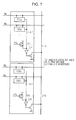
- FIGS. 6A and 6B to FIG. 8 are diagrams of circuit configurations in the past.
- a semiconductor memory device includes a first memory circuits connecting to a first bit line, a second bit line and a word line, a first pre-charge control circuit connecting to a first pre-charge control line, the first bit line and the second bit line and that pre-charges the first bit line and the second bit line on the basis of the input from the first pre-charge control line, and a read control circuit having a first transistor, a second transistor, a third transistor and a fourth transistor, wherein the fourth transistor is brought into conduction on the basis of the input from a charged global-bit-line driver control line, the column having the first bit line and the second bit line is thus selected, and the information held in the memory circuit connecting to the driven word line among the memory circuits is output to the third bit line.
- a semiconductor memory circuit and a control method for reading data according to an embodiment will be described in detail below.
- a semiconductor memory circuit according to a first embodiment includes a read circuit, which is a dynamic circuit having a bit line connecting to a single p-type transistor.
- the read circuit includes a p-type transistor that is located in series between another p-type transistor connecting to the bit line and a power supply and is connected to a read-column selection line.
- the second feature is that the read circuit further includes an n-type transistor connecting to a read-column selection line.
- FIG. 1 is a diagram illustrating a circuit configuration of the semiconductor memory circuit according to the first embodiment.
- FIG. 2 is a diagram for explaining the semiconductor memory circuit according to the first embodiment.
- This semiconductor memory circuit has a circuit configuration as illustrated in FIG. 1 . With reference to FIG. 2 , this semiconductor memory circuit will be described below.
- the semiconductor memory circuit includes a plurality of bit cells 10 that connect to local bit lines 70 and word lines 20 and hold information.
- the semiconductor memory circuit further includes a pre-charge circuit 30 that connects to a local bit line pre-charge line 40 and the local bit lines 70 and pre-charges the local bit lines 70 on the basis of the input from the local bit line pre-charge line 40.
- the semiconductor memory circuit further includes a read circuit 200 as will be described below. That is, the read circuit 200 has a p-type transistor P2 having a source terminal connected to a power supply and a gate terminal connected to a read-column selection line 90.
- the read circuit 200 further has a p-type transistor P1 that has a source terminal connected to the drain terminal of the p-type transistor P2, a gate terminal connected to one of the local bit lines, and a drain terminal connected to a sense out line 80 and, on the basis of the input from the read-column selection line 90 and the potential level of the local bit line 70, charges the sense out line 80.
- the read circuit 200 further has an n-type transistor N1 that has a drain terminal connected to the sense out line 80, a gate terminal connected to the read-column selection line 90 and a source terminal grounded and pre-discharges the global-bit-line driver control line on the basis of a column selection signal.
- the read circuit 200 further has an n-type transistor N2 that has a drain terminal connected to a global bit line, a gate terminal connected to the sense out line 80 and a source terminal grounded.
- the n-type transistor N2 is brought into conduction.
- the column having the corresponding local bit line is selected (which means that when the signal on the read-column selection line 90 is changed to "Lo", the corresponding column is selected thereby), and the information held in the bit cell 10 having the word line 20 driven among the plurality of bit cells 10 is read from a global bit line 110.
- the semiconductor memory circuit according to the first embodiment further includes, as illustrated in FIG. 2 , a write circuit 300 connecting to a write-column-selection line 310 and a write data input line 320.
- a write circuit 300 connecting to a write-column-selection line 310 and a write data input line 320.
- the column having the corresponding local bit line is selected, and the data is written from the write data input line 320 to the bit cell 10 having the word line 20 driven among the plurality of bit cells 10.
- the bit cell 10 may also be referred to as "bit cell”; the word line 20 may also be referred to as “word line”; the pre-charge circuit 30 may also be referred to as "first pre-charge control circuit”; the local bit line pre-charge line 40 may also be referred to as “first pre-charge control line”; the local bit line 70 may also be referred to as “first bit line” or “second bit line”; the sense out line 80 may also be referred to as “global-bit-line driver control line”; the read-column selection line 90 may also be referred to as “column selection line”; the global bit line pre-charge line 100 may also be referred to as “third pre-charge control line,” and the global bit line 110 may also be referred to as "third bit line.”
- the p-type transistor P1 may also be referred to as "second transistor”; the p-type transistor P2 may also be referred to as “first transistor”; the n-type transistor N1 may also be referred to as “third transistor,” and the n-type transistor N2 may also be referred to as "fourth transistor.”
- the write circuit 300 may also be referred to as "writing control circuit”; the write-column-selection line 310 may also be referred to as “write-column-selection line,” and the write data input line 320 may also be referred to as "write data input line.”
- FIG. 3 is a diagram for explaining the semiconductor memory circuit according to the first embodiment.
- FIG. 1 and FIG. 2 illustrate only a single line of the bit cells 10, for simplification.
- the plurality of bit cells is arranged in a semiconductor memory circuit.
- the bit cell 10 holding the data corresponding to the read request in the read circuit 200 is selected. More specifically, as illustrated in FIG. 3 , the word line 20 is driven, and the row connecting to the bit cell 10 holding the data corresponding to the read request is selected thereby. Then, on the basis of the input from the read-column selection line 90, the column connecting to the bit cell holding the data corresponding to the read request is selected.
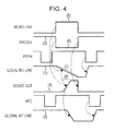
- FIG. 4 is a diagram illustrating signal waveforms according to the first embodiment.
- the illustrated dashed arrow indicates signals that trigger the switching between "Hi" and "Lo" of the signals.
- the local bit line 70 is pre-charged.
- the global bit line 110 is pre-charged. (Refer to (2) in FIG. 4 ).
- the input from the read-column selection line 90 has "Hi". (Refer to (3) in FIG. 4 ).
- the n-type transistor N1 connected to the read-column selection line 90 is turned on, and the sense out line 80 is pre-discharged. As a result, the sense out line 80 is "Lo". (Refer to (4) in FIG. 4 ).
- the word line 20 is "Hi". (Refer to (5) in FIG. 4 ).
- the n-type transistor N1 is turned off. Since the input from the read-column selection line 90 has been changed to have “Lo”, the corresponding column has already been selected.
- the p-type transistor P2 is turned on.
- the local bit line 70 is discharged (which means that, when the internal node of the bit cell relating to the local bit line 70 is "Lo”, the local bit line 70 is discharged, and when it is "Hi", the local bit line 70 is not discharged).
- the p-type transistor P1 is turned on.
- both of the p-type transistors P1 and P2 are turned on, charges are thus loaded from the power supply, and the sense out line 80 is charged. (Refer to (8) in FIG. 4 ).
- the sense out line 80 having "Hi” turns on the n-type transistor N2.
- the global bit line 110 is discharged to "Lo".
- "Lo" is output to the I/O circuit 400 as the reading result from the bit cell 10.
- the reading operation in the read circuit 200 will be organized conceptually. (1): The entire row driven by a word line is read. (2): In the row, the column required by a read-column selection signal is only selected (where the column has been already selected at that time). (3): As a result, the sense out is charged. (4): The sense out charged in (3) turns on the n-type transistor N2, and, as a result, the data in the memory/holding circuit selected by the word line and read-column selection signal is read (where the n-type transistor N2 is a circuit for transmitting the result read in the local region to the global region).
- the semiconductor memory circuit according to the first embodiment includes the read circuit having a dynamic configuration connecting a bit line to the p-type transistor P1, the speed of discharging from the local bit line 70 may be increased. As a result, the reading speed by the read circuit 200 may be increased.
- the semiconductor memory circuit according to the first embodiment includes the read circuit internally having the p-type transistor P2 connected in series to between a p-type transistor P1 connected to the local bit line 70 and the power supply and connecting to the read-column selection signal. Since the p-type transistor P2 may implement the column selection of a bit cell, the number of global bit line to be charged or discharged may be reduced. As a result, the power consumption may be reduced.
- the n-type transistor N1 for pre-discharging the sense out line 80 is connected to a read-column selection signal.
- one signal line may be required for column selection and pre-discharging the sense out line 80.
- the size of the circuit may be reduced.
- a semiconductor memory circuit and a control method for writing/reading data according to another embodiment will be described below.
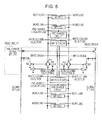
- FIG. 5 is a diagram illustrating a configuration of a semiconductor memory circuit according to the second embodiment.
- the components of the semiconductor memory circuit illustrated in FIG. 1 are not always physically required to be arranged as in the illustrated configuration.
- the concrete forms of the distribution and integration of the components of the semiconductor memory circuit illustrated in FIG. 1 are not limited to the illustrated one, but all or a part of the components may be functionally or physically distributed and/or integrated in arbitrary units in accordance with the loads and/or the usages, within the range required for achieving the object of the embodiment.
- a control method for reading data in the semiconductor memory circuit including a reading control step of performing reading control including, on the basis of the input from the pre-charged sense out line 80, bringing the n-type transistor N2 into conduction, selecting the column having the corresponding local bit line, and outputting the information held in the bit cell 10 having the word line 20 driven among the plurality of bit cells 10 to the global bit line 110.
Landscapes
- Engineering & Computer Science (AREA)
- Microelectronics & Electronic Packaging (AREA)
- Computer Hardware Design (AREA)
- Dram (AREA)
- Static Random-Access Memory (AREA)
- Read Only Memory (AREA)
Abstract
Description
- The embodiment discussed herein are related to semiconductor memory circuit and control method for reading data.
- Hitherto, in order to store various data in a semiconductor integrated circuit, a semiconductor memory circuit such as an SRAM (static random access memory) and a DRAM (dynamic random access memory) have been used.
- [Patent Document 1] Japanese Laid-open Patent Publication No.
2006-331568 - [Non patent Document 2] J. Davis, D. Plass, P. Bunce, Y. Chanl, A. Pelella, R. Joshi, A. Chen, W. Huott, T. Knips, P. Patel, K. Lo, E. Fluhr "A 5.6 GHz 64 kB Dual-Read Data Cache for the POWER6TM Processor" IEEE International Solid-State Circuits Conference, 2006.
- The semiconductor memory circuit has adopted a dynamic circuit in which a single p-type MOS transistor connects to a single bit line. The adoption of the dynamic circuit may reduce the load capacity of the bit line more than a static circuit because only one transistor connects to the bit line and thus may increase the operation speed. Also, since the dynamic circuit may be configured by a lower number of transistors, which may reduce the circuit area.
- The semiconductor memory circuit in the past having a column selection circuit in the local bit line as illustrated in
FIG. 6A has a lower discharge speed of the local bit line, resulting in a decrease in reading speed. - As illustrated in
FIGS. 6A and 6B andFIG. 7 , the addition of a local read circuit configured by two or more transistors such as an inverter and a NAND to the end of the local bit line may reduce the discharge speed of the local bit line. As a result, the reading speed of the semiconductor memory circuit may decrease. - As illustrated in
FIG. 7 andFIG. 8 , the column selection in global reading instead of column selection in local reading using a local read circuit (hereinafter also referred to as "local region") may possibly include charging/discharging in the global bit line for all columns, which may increase the power consumption. - In
FIG. 8 , the reading speed is increased by a pre-discharge dynamic circuit having the end of the local bit line connecting to one p-type transistor. (Refer to (A) inFIG. 8 ). However, since, as described above, the column selection is not performed in the local region, the power consumption disadvantageously increases. For example, the addition of a column selection circuit to the circuit illustrated inFIG. 8 may also necessarily increase the number of transistors. Both of a pre-discharge signal and column selection signal may be required to input to the local region, which may also require the wiring area there for. For these reasons, building the column selection circuit into the circuit illustrated inFIG. 8 increases the size of circuit.FIGS. 6A and 6B toFIG. 8 are diagrams of circuit configurations in the past. - According to an aspect of embodiments, a semiconductor memory device includes a first memory circuits connecting to a first bit line, a second bit line and a word line, a first pre-charge control circuit connecting to a first pre-charge control line, the first bit line and the second bit line and that pre-charges the first bit line and the second bit line on the basis of the input from the first pre-charge control line, and a read control circuit having a first transistor, a second transistor, a third transistor and a fourth transistor, wherein the fourth transistor is brought into conduction on the basis of the input from a charged global-bit-line driver control line, the column having the first bit line and the second bit line is thus selected, and the information held in the memory circuit connecting to the driven word line among the memory circuits is output to the third bit line.
- Preferred features of the present invention will now be described, purely by way of example, with reference to the accompanying drawings, in which:-
-
-
FIG. 1 is a diagram illustrating a circuit configuration of a semiconductor memory circuit according to a first embodiment; -
FIG. 2 is a diagram for explaining the semiconductor memory circuit according to the first embodiment; -
FIG. 3 is a diagram for explaining the semiconductor memory circuit according to the first embodiment; -
FIG. 4 is a diagram illustrating signal waveforms according to the first embodiment; -
FIG. 5 is a diagram illustrating a circuit configuration of a semiconductor memory circuit according to a second embodiment; -
FIGs 6A and 6B are diagrams of circuit configurations in the past; -
FIG. 7 is a diagram of circuit configuration in the past; and -
FIG. 8 is a diagram of circuit configuration in the past. - A semiconductor memory circuit and a control method for reading data according to an embodiment will be described in detail below.
A semiconductor memory circuit according to a first embodiment includes a read circuit, which is a dynamic circuit having a bit line connecting to a single p-type transistor. There are two essential features of the semiconductor memory circuit according to the first embodiment. The first feature is that the read circuit includes a p-type transistor that is located in series between another p-type transistor connecting to the bit line and a power supply and is connected to a read-column selection line. The second feature is that the read circuit further includes an n-type transistor connecting to a read-column selection line. The semiconductor memory circuit according to the first embodiment will be described more specifically below. -
FIG. 1 is a diagram illustrating a circuit configuration of the semiconductor memory circuit according to the first embodiment.FIG. 2 is a diagram for explaining the semiconductor memory circuit according to the first embodiment. This semiconductor memory circuit has a circuit configuration as illustrated inFIG. 1 . With reference toFIG. 2 , this semiconductor memory circuit will be described below. - As illustrated in
FIG. 2 , the semiconductor memory circuit according to the first embodiment includes a plurality ofbit cells 10 that connect tolocal bit lines 70 andword lines 20 and hold information. - The semiconductor memory circuit further includes a
pre-charge circuit 30 that connects to a local bit line pre-chargeline 40 and thelocal bit lines 70 and pre-charges thelocal bit lines 70 on the basis of the input from the local bit line pre-chargeline 40. - The semiconductor memory circuit further includes a
read circuit 200 as will be described below. That is, theread circuit 200 has a p-type transistor P2 having a source terminal connected to a power supply and a gate terminal connected to a read-column selection line 90. - The
read circuit 200 further has a p-type transistor P1 that has a source terminal connected to the drain terminal of the p-type transistor P2, a gate terminal connected to one of the local bit lines, and a drain terminal connected to a sense outline 80 and, on the basis of the input from the read-column selection line 90 and the potential level of thelocal bit line 70, charges the sense outline 80. Theread circuit 200 further has an n-type transistor N1 that has a drain terminal connected to the sense outline 80, a gate terminal connected to the read-column selection line 90 and a source terminal grounded and pre-discharges the global-bit-line driver control line on the basis of a column selection signal. Theread circuit 200 further has an n-type transistor N2 that has a drain terminal connected to a global bit line, a gate terminal connected to the sense outline 80 and a source terminal grounded. - In the
read circuit 200, on the basis of the input from the charged sense outline 80, the n-type transistor N2 is brought into conduction. Thus, the column having the corresponding local bit line is selected (which means that when the signal on the read-column selection line 90 is changed to "Lo", the corresponding column is selected thereby), and the information held in thebit cell 10 having theword line 20 driven among the plurality ofbit cells 10 is read from aglobal bit line 110. - The semiconductor memory circuit according to the first embodiment further includes, as illustrated in
FIG. 2 , awrite circuit 300 connecting to a write-column-selection line 310 and a write data input line 320. On the basis of the input from the write-column-selection line 310, the column having the corresponding local bit line is selected, and the data is written from the write data input line 320 to thebit cell 10 having theword line 20 driven among the plurality ofbit cells 10. - According to an embodiment, the
bit cell 10 may also be referred to as "bit cell"; theword line 20 may also be referred to as "word line"; thepre-charge circuit 30 may also be referred to as "first pre-charge control circuit"; the local bit line pre-chargeline 40 may also be referred to as "first pre-charge control line"; thelocal bit line 70 may also be referred to as "first bit line" or "second bit line"; the sense outline 80 may also be referred to as "global-bit-line driver control line"; the read-column selection line 90 may also be referred to as "column selection line"; the global bit line pre-chargeline 100 may also be referred to as "third pre-charge control line," and theglobal bit line 110 may also be referred to as "third bit line." - According to an embodiment, the p-type transistor P1 may also be referred to as "second transistor"; the p-type transistor P2 may also be referred to as "first transistor"; the n-type transistor N1 may also be referred to as "third transistor," and the n-type transistor N2 may also be referred to as "fourth transistor."
- According to an embodiment, the
write circuit 300 may also be referred to as "writing control circuit"; the write-column-selection line 310 may also be referred to as "write-column-selection line," and the write data input line 320 may also be referred to as "write data input line." - With reference to
FIG. 3 , a bit-cell selecting method in theread circuit 200 will be described below.FIG. 3 is a diagram for explaining the semiconductor memory circuit according to the first embodiment.FIG. 1 andFIG. 2 illustrate only a single line of thebit cells 10, for simplification. Generally, as illustrated inFIG. 3 , the plurality of bit cells is arranged in a semiconductor memory circuit. - For example, in response to a read request from a host, not depicted, the
bit cell 10 holding the data corresponding to the read request in theread circuit 200 is selected. More specifically, as illustrated inFIG. 3 , theword line 20 is driven, and the row connecting to thebit cell 10 holding the data corresponding to the read request is selected thereby. Then, on the basis of the input from the read-column selection line 90, the column connecting to the bit cell holding the data corresponding to the read request is selected. - Next, with reference to
FIG. 4 , a reading operation routine in theread circuit 200 will be described.FIG. 4 is a diagram illustrating signal waveforms according to the first embodiment. The illustrated dashed arrow indicates signals that trigger the switching between "Hi" and "Lo" of the signals. In response to a read request and then on the basis of the input from the local bit line pre-charge line, thelocal bit line 70 is pre-charged. (Refer to (1) inFIG. 4 ). Next, on the basis of the input from the global bit linepre-charge line 100, theglobal bit line 110 is pre-charged. (Refer to (2) inFIG. 4 ). - As illustrated in
FIG. 4 , during the pre-charge on thelocal bit line 70 andglobal bit line 110, the input from the read-column selection line 90 has "Hi". (Refer to (3) inFIG. 4 ). Thus, the n-type transistor N1 connected to the read-column selection line 90 is turned on, and the sense outline 80 is pre-discharged. As a result, the sense outline 80 is "Lo". (Refer to (4) inFIG. 4 ). - Then, the
word line 20 is "Hi". (Refer to (5) inFIG. 4 ). When the input from the read-column selection line 90 is "Lo" (as in (6) inFIG. 4 ), the n-type transistor N1 is turned off. Since the input from the read-column selection line 90 has been changed to have "Lo", the corresponding column has already been selected. On the other hand, when the input from the read-column selection line 90 is "Lo" (as in (6) inFIG. 4 ), the p-type transistor P2 is turned on. Conversely, when theword line 20 is "Hi", thelocal bit line 70 is discharged (which means that, when the internal node of the bit cell relating to thelocal bit line 70 is "Lo", thelocal bit line 70 is discharged, and when it is "Hi", thelocal bit line 70 is not discharged). (Refer to (7) inFIG. 4 ). Thus, the p-type transistor P1 is turned on. When both of the p-type transistors P1 and P2 are turned on, charges are thus loaded from the power supply, and the sense outline 80 is charged. (Refer to (8) inFIG. 4 ). - The sense out
line 80 having "Hi" turns on the n-type transistor N2. Thus, theglobal bit line 110 is discharged to "Lo". After theglobal bit line 110 is discharged, "Lo" is output to the I/O circuit 400 as the reading result from thebit cell 10. - The reading operation in the
read circuit 200 will be organized conceptually. (1): The entire row driven by a word line is read. (2): In the row, the column required by a read-column selection signal is only selected (where the column has been already selected at that time). (3): As a result, the sense out is charged. (4): The sense out charged in (3) turns on the n-type transistor N2, and, as a result, the data in the memory/holding circuit selected by the word line and read-column selection signal is read (where the n-type transistor N2 is a circuit for transmitting the result read in the local region to the global region). - As described above, since the semiconductor memory circuit according to the first embodiment includes the read circuit having a dynamic configuration connecting a bit line to the p-type transistor P1, the speed of discharging from the
local bit line 70 may be increased. As a result, the reading speed by theread circuit 200 may be increased. - A semiconductor memory circuit in the past has shorter local bit lines as a measure against the variations among the performance for manufacturing transistors. However, the increase in number of divisions of bit lines increases the size of the layout in the direction of the bit lines. Thus, the amount of amount of charges charge to be loaded or unloaded to or from a global bit line increases. As a result, the power consumption increases. On the other hand, the semiconductor memory circuit according to the first embodiment includes the read circuit internally having the p-type transistor P2 connected in series to between a p-type transistor P1 connected to the
local bit line 70 and the power supply and connecting to the read-column selection signal. Since the p-type transistor P2 may implement the column selection of a bit cell, the number of global bit line to be charged or discharged may be reduced. As a result, the power consumption may be reduced. - Within the
read circuit 200, the n-type transistor N1 for pre-discharging the sense outline 80 is connected to a read-column selection signal. Thus, one signal line may be required for column selection and pre-discharging the sense outline 80. Thus, the size of the circuit may be reduced. - A semiconductor memory circuit and a control method for writing/reading data according to another embodiment will be described below.
- For example, as illustrated in
FIG. 5 , the semiconductor memory circuit according to the first embodiment is applicable to a multiport semiconductor memory circuit.FIG. 5 is a diagram illustrating a configuration of a semiconductor memory circuit according to the second embodiment. - The components of the semiconductor memory circuit illustrated in
FIG. 1 are not always physically required to be arranged as in the illustrated configuration. In other words, the concrete forms of the distribution and integration of the components of the semiconductor memory circuit illustrated inFIG. 1 are not limited to the illustrated one, but all or a part of the components may be functionally or physically distributed and/or integrated in arbitrary units in accordance with the loads and/or the usages, within the range required for achieving the object of the embodiment. - The semiconductor memory circuit according to the first embodiment may implement the control method for reading data as follows:
- There may be provided a control method for reading data in the semiconductor memory circuit, the method including a reading control step of performing reading control including, on the basis of the input from the pre-charged sense out
line 80, bringing the n-type transistor N2 into conduction, selecting the column having the corresponding local bit line, and outputting the information held in thebit cell 10 having theword line 20 driven among the plurality ofbit cells 10 to theglobal bit line 110.
Claims (10)
- A semiconductor memory device comprising:a first plurality of memory circuits that connect to a first bit line, a second bit line, and a word line, and that hold information;a first pre-charge control circuit that connects to a first pre-charge control line, the first bit line, and the second bit line and that pre-charges the first bit line and the second bit line on the basis of the input from the first pre-charge control line; anda read control circuit having a first transistor that has a source terminal connected to a power supply and a gate terminal connected to a read-column selection line; a second transistor that has a source terminal connected to a drain terminal of the first transistor, a gate terminal connected to the first bit line, and a drain terminal connected to a global-bit-line driver control line and that charges the global-bit-line driver control line on the basis of the input from the read-column selection line and the potential level of the first bit line; a third transistor that has a drain terminal connected to the global-bit-line driver control line, a gate terminal connected to the read-column selection line, and a source terminal grounded and that pre-discharges the global-bit-line driver control line on the basis of column selection signal; and a fourth transistor that has a drain terminal connected to a third bit line, a gate terminal connected to the global-bit-line driver control line, and a source terminal grounded, wherein the fourth transistor is brought into conduction on the basis of the input from the charged global-bit-line driver control line, the column having the first bit line and the second bit line is thus selected, and the information held in the memory circuit connecting to the driven word line among the first plurality of memory circuits is output to the third bit line.
- The semiconductor memory device according to claim 1, further comprising:a second plurality of memory circuits that connect to a fourth bit line, a fifth bit line, and a word line and that hold information;a first pre-charge control circuit that connects to a second pre-charge control line, the fourth bit line, and the fifth bit line and that pre-charges the fourth bit line and the fifth bit line on the basis of the input from the second pre-charge control line; anda fifth transistor that has a source terminal connected to the drain terminal of the first transistor, a gate terminal connected to the fourth bit line, and a drain terminal connected to a global-bit-line driver control line and that charges the global-bit-line driver control line on the basis of the input from the read-column selection line and the potential level of the fourth bit line.
- The semiconductor memory device according to claim 1 or 2, further comprising:a sixth transistor that has a source terminal connected to the power supply, a gate terminal connected to a third pre-charge control line, and a source terminal connected to the third bit line, wherein the third bit line is pre-charged on the basis of the input from the third pre-charge control line.
- The semiconductor memory device according to claim 1 or 2, further comprising:a sixth transistor that has a source terminal connected to the power supply, a gate terminal connected to a third pre-charge control line, and a source terminal connected to the third bit line, wherein the third bit line is pre-charged on the basis of the input from the third pre-charge control line.
- The semiconductor memory device according to any of claims 1 to 4, further comprising:a control circuit that writes data connecting to a write-column-selection line and a write data input line, wherein:a column having the second bit line and the first bit line is selected on the basis of the input from the write-column-selection line, and data from the write data input line is written to a memory circuit connecting to the driven word line among the first plurality of memory circuits and the second plurality of memory circuits.
- The semiconductor memory device according to claim 2, or any of claims 3 to 5 when read as appended to claim 2, further comprising:a control circuit that writes data connecting to a write-column-selection line and a write data input line, wherein:a column having the second bit line and the first bit line is selected on the basis of the input from the write-column-selection line, and data from the write data input line is written to a memory circuit connecting to the driven word line among the first plurality of memory circuits and the second plurality of memory circuits.
- A semiconductor memory device comprising:a plurality of memory circuits that connect to a first bit line, a second bit line, and a word line and that hold information;a pre-charge control circuit that connects to a first pre-charge control line, the first bit line, and the second bit line and that pre-charges the first bit line and the second bit line on the basis of the input from the first pre-charge control line; anda first read control circuit having a first transistor that has a source terminal connected to a power supply and a gate terminal connected to a read-column selection line; a second transistor that has a source terminal connected to a drain terminal of the first transistor, a gate terminal connected to the first bit line, and a drain terminal connected to a first global-bit-line driver control line and that charges the first global-bit-line driver control line on the basis of the input from the read-column selection line and the potential level of the first bit line; a third transistor that has a drain terminal connected to the global-bit-line driver control line, a gate terminal connected to the read-column selection line, and a source terminal grounded; and a fourth transistor that has a drain terminal connected to a third bit line, a gate terminal connected to the first global-bit-line driver control line, and a source terminal grounded, wherein the column having the first bit line and the second bit line is thus selected on the basis of the input from the pre-charged first global-bit-line driver control line, the fourth transistor is brought into conduction, and the information held in the memory circuit connecting to the driven word line among the plurality of memory circuits is output to the third bit line; anda second read control circuit having a fifth transistor that has a source terminal connected to a power supply and a gate terminal connected to a read-column selection line; and a sixth transistor that has a source terminal connected to a drain terminal of the fifth transistor, a gate terminal connected to the second bit line, and a drain terminal connected to a second global-bit-line driver control line and, that charges the second global-bit-line driver control line on the basis of the input from the second read-column selection line and the potential level of the second bit line; a seventh transistor that has a drain terminal connected to the global-bit-line driver control line, a gate terminal connected to the second read-column selection line, and a source terminal grounded and that pre-discharges the global-bit-line driver control line on the basis of column selection signal; and an eighth transistor that has a drain terminal connected to a fourth bit line, a gate terminal connected to the second global-bit-line driver control line, and a source terminal grounded, wherein the eighth transistor is brought into conduction on the basis of the input from the pre-charged second global-bit-line driver control line, the column having the first bit line and the second bit line is thus selected, and the information held in the memory circuit connecting to the driven word line among the plurality of memory circuits is output to the fourth bit line.
- A control method for reading data in a semiconductor memory device, the semiconductor memory device having:a first plurality of memory circuits that connect to a first bit line, a second bit line, and a word line and that hold information;a first pre-charge control circuit that connects to a first pre-charge control line, the first bit line, and the second bit line and that pre-charges the first bit line and the second bit line on the basis of the input from the first pre-charge control line; anda read control circuit having a first transistor that has a source terminal connected to a power supply and a gate terminal connected to a read-column selection line, a second transistor that has a source terminal connected to a drain terminal of the first transistor, a gate terminal connected to the first bit line, and a drain terminal connected to a global-bit-line driver control line and that charges the global-bit-line driver control line on the basis of the input from the read-column selection line and the potential level of the first bit line; a third transistor that has a drain terminal connected to the global-bit-line driver control line, a gate terminal connected to the read-column selection line, and a source terminal grounded and that pre-discharges the global-bit-line driver control line on the basis of column selection signal; and a fourth transistor that has a drain terminal connected to a third bit line, a gate terminal connected to the global-bit-line driver control line, and a source terminal grounded, the control method for reading data comprising :selecting the column having the first bit line and the second bit line, by bringing the fourth transistor into conduction on the basis of the input from the charged global-bit-line driver control line; andoutputting the information held in the memory circuit connecting to the driven word line among the first plurality of memory circuits to the third bit line.
- A control method for writing data in a semiconductor memory device, the semiconductor memory device having:a first plurality of memory circuits that connect to a first bit line, a second bit line, and a word line and that hold information; anda control circuit that writes data connecting to a write-column-selection line and a write data input line, the control method for writing data comprising:selecting the column having the first bit line and the second bit line on the basis of the input from the write-column-selection line; andwriting data from the write data input line to a memory circuit connecting to the driven word line among the first plurality of memory circuits.
- A control method for reading data in a semiconductor memory device, the semiconductor memory device having:a plurality of memory circuits that connect to a first bit line, a second bit line, and a word line and that hold information;a pre-charge control circuit that connects to a first pre-charge control line, the first bit line, and the second bit line and that pre-charges the first bit line and the second bit line on the basis of the input from the first pre-charge control line; anda first read control circuit having a first transistor that has a source terminal connected to a power supply and a gate terminal connected to a read-column selection line; a second transistor that has a source terminal connected to a drain terminal of the first transistor, a gate terminal connected to the first bit line, and a drain terminal connected to a first global-bit-line driver control line and that charges the first global-bit-line driver control line on the basis of the input from the read-column selection line and the potential level of the first bit line; a third transistor that has a drain terminal connected to the global-bit-line driver control line, a gate terminal connected to the read-column selection line, and a source terminal grounded; and a fourth transistor that has a drain terminal connected to a third bit line, a gate terminal connected to the first global-bit-line driver control line, and a source terminal grounded, wherein the fourth transistor is brought into conduction on the basis of the input from the charged first global-bit-line driver control line, the column having the first bit line and the second bit line is thus selected, and the information held in a memory circuit connecting to the driven word line among the plurality of memory circuits is output to the third bit line; anda second read control circuit having a fifth transistor that has a source terminal connected to a power supply and a gate terminal connected to a read-column selection line; and a sixth transistor that has a source terminal connected to a drain terminal of the fifth transistor, a gate terminal connected to the second bit line, and a drain terminal connected to a second global-bit-line driver control line and, on the basis of the input from the second read-column selection line and the potential level of the second bit line, that charges the second global-bit-line driver control line; a seventh transistor that has a drain terminal connected to the global-bit-line driver control line, a gate terminal connected to the second read-column selection line, and a source terminal grounded; and an eighth transistor that has a drain terminal connected to a fourth bit line, a gate terminal connected to the second global-bit-line driver control line, and a source terminal grounded, wherein the eighth transistor is brought into conduction on the basis of the input from the charged second global-bit-line driver control line, the column having the first bit line and the second bit line is thus selected, and the information held in the memory circuit connecting to the driven word line among the plurality of memory circuits is output to the fourth bit line, the control method for reading data comprising:selecting the column having the first bit line and the second bit line by bringing the fourth transistor into conduction on the basis of the input from the charged first global-bit-line driver control line;reading the information held in the memory circuit connecting to the driven word line among the plurality of memory circuits from the third bit line;selecting the column having the first bit line and the second bit line by bringing the eighth transistor into conduction on the basis of the input from the charged second global-bit-line driver control line; andreading the information held in the memory circuit connecting to the driven word line among the plurality of memory circuits to the fourth bit line.
Applications Claiming Priority (1)
| Application Number | Priority Date | Filing Date | Title |
|---|---|---|---|
| JP2009014755A JP2010170641A (en) | 2009-01-26 | 2009-01-26 | Semiconductor memory circuit device and read control method |
Publications (3)
| Publication Number | Publication Date |
|---|---|
| EP2211352A2 true EP2211352A2 (en) | 2010-07-28 |
| EP2211352A3 EP2211352A3 (en) | 2010-12-15 |
| EP2211352B1 EP2211352B1 (en) | 2012-06-20 |
Family
ID=42194821
Family Applications (1)
| Application Number | Title | Priority Date | Filing Date |
|---|---|---|---|
| EP10151066A Not-in-force EP2211352B1 (en) | 2009-01-26 | 2010-01-19 | Semiconductor memory circuit and control method for reading data |
Country Status (5)
| Country | Link |
|---|---|
| US (2) | US8335120B2 (en) |
| EP (1) | EP2211352B1 (en) |
| JP (1) | JP2010170641A (en) |
| KR (1) | KR101054322B1 (en) |
| CN (1) | CN101789261B (en) |
Cited By (1)
| Publication number | Priority date | Publication date | Assignee | Title |
|---|---|---|---|---|
| WO2021228953A1 (en) | 2020-05-12 | 2021-11-18 | Xenergic | Precharge circuitry for memory |
Families Citing this family (13)
| Publication number | Priority date | Publication date | Assignee | Title |
|---|---|---|---|---|
| US8488396B2 (en) * | 2010-02-04 | 2013-07-16 | Taiwan Semiconductor Manufacturing Company, Ltd. | Dual rail static random access memory |
| WO2012124063A1 (en) * | 2011-03-15 | 2012-09-20 | 富士通株式会社 | Semiconductor recording device and method for controlling semiconductor recording device |
| JP5760829B2 (en) * | 2011-08-09 | 2015-08-12 | 富士通セミコンダクター株式会社 | Static RAM |
| US8570791B2 (en) * | 2011-10-05 | 2013-10-29 | Taiwan Semiconductor Manufacturing Co., Ltd. | Circuit and method of word line suppression |
| WO2013099014A1 (en) * | 2011-12-28 | 2013-07-04 | 富士通株式会社 | Semiconductor memory device and control method of a semiconductor memory device |
| US9153302B2 (en) * | 2012-01-31 | 2015-10-06 | Taiwan Semiconductor Manufacturing Company, Ltd. | Memory and method of operating the same |
| US20140092672A1 (en) * | 2012-09-28 | 2014-04-03 | International Business Machines Corporation | Power management domino sram bit line discharge circuit |
| US9007857B2 (en) * | 2012-10-18 | 2015-04-14 | International Business Machines Corporation | SRAM global precharge, discharge, and sense |
| CN104978999A (en) * | 2014-04-03 | 2015-10-14 | 晶宏半导体股份有限公司 | Bit line multiplexer with precharge |
| US9208859B1 (en) * | 2014-08-22 | 2015-12-08 | Globalfoundries Inc. | Low power static random access memory (SRAM) read data path |
| CN105957552B (en) * | 2016-04-21 | 2018-12-14 | 华为技术有限公司 | memory |
| JP2019164856A (en) | 2018-03-19 | 2019-09-26 | 株式会社東芝 | Semiconductor storage device |
| US20240412766A1 (en) * | 2023-06-08 | 2024-12-12 | Taiwan Semiconductor Manufacturing Company, Ltd. | Pre-Charger Circuit of Memory Device and Methods For Operating The Same |
Citations (1)
| Publication number | Priority date | Publication date | Assignee | Title |
|---|---|---|---|---|
| JP2006331568A (en) | 2005-05-27 | 2006-12-07 | Nec Electronics Corp | External clock synchronous semiconductor storage device and its control method |
Family Cites Families (13)
| Publication number | Priority date | Publication date | Assignee | Title |
|---|---|---|---|---|
| KR100356795B1 (en) * | 1999-12-23 | 2002-10-19 | 주식회사 하이닉스반도체 | Sram having write driver circuit |
| JP2002100188A (en) * | 2000-09-25 | 2002-04-05 | Mitsubishi Electric Corp | Semiconductor storage device |
| KR100380347B1 (en) * | 2000-11-21 | 2003-04-11 | 삼성전자주식회사 | Semiconductor memory device and data read method thereof |
| JP2003223788A (en) * | 2002-01-29 | 2003-08-08 | Hitachi Ltd | Semiconductor integrated circuit device |
| JP2004079099A (en) * | 2002-08-20 | 2004-03-11 | Fujitsu Ltd | Semiconductor memory |
| JP4005535B2 (en) * | 2003-07-02 | 2007-11-07 | 松下電器産業株式会社 | Semiconductor memory device |
| WO2005041203A1 (en) * | 2003-10-27 | 2005-05-06 | Nec Corporation | Semiconductor storage device |
| KR100583959B1 (en) * | 2004-01-07 | 2006-05-26 | 삼성전자주식회사 | Semiconductor memory device and data writing and reading method thereof |
| KR100555568B1 (en) * | 2004-08-03 | 2006-03-03 | 삼성전자주식회사 | Semiconductor memory device with local sense amplification circuit capable of on / off control |
| JP4912016B2 (en) * | 2005-05-23 | 2012-04-04 | ルネサスエレクトロニクス株式会社 | Semiconductor memory device |
| JP2008176910A (en) * | 2006-12-21 | 2008-07-31 | Matsushita Electric Ind Co Ltd | Semiconductor memory device |
| US7499312B2 (en) * | 2007-01-05 | 2009-03-03 | International Business Machines Corporation | Fast, stable, SRAM cell using seven devices and hierarchical bit/sense line |
| JP5298644B2 (en) * | 2008-05-30 | 2013-09-25 | 富士通株式会社 | Memory circuit and control method |
-
2009
- 2009-01-26 JP JP2009014755A patent/JP2010170641A/en active Pending
-
2010
- 2010-01-12 US US12/685,854 patent/US8335120B2/en not_active Expired - Fee Related
- 2010-01-18 KR KR1020100004229A patent/KR101054322B1/en not_active Expired - Fee Related
- 2010-01-19 EP EP10151066A patent/EP2211352B1/en not_active Not-in-force
- 2010-01-20 CN CN2010100042805A patent/CN101789261B/en not_active Expired - Fee Related
-
2012
- 2012-09-24 US US13/625,461 patent/US20130077424A1/en not_active Abandoned
Patent Citations (1)
| Publication number | Priority date | Publication date | Assignee | Title |
|---|---|---|---|---|
| JP2006331568A (en) | 2005-05-27 | 2006-12-07 | Nec Electronics Corp | External clock synchronous semiconductor storage device and its control method |
Non-Patent Citations (2)
| Title |
|---|
| J. DAVIS; D. PLASS; P. BUNCE; Y. CHANL; A. PELELLA; R. JOSHI; A. CHEN; W. HUOTT; T. KNIPS; P. PATEL: "A 5.6 GHz 64 kB Dual-Read Data Cache for the POWER6TM Processor", IEEE INTERNATIONAL SOLID-STATE CIRCUITS CONFERENCE, 2006 |
| KEVIN ZHANG; KEN HOSE; VIVEK DE; BORYS SENYK: "The Scaling of Data Sensing Schemes for High Speed Cache Design in Sub-0. 18 pm Technologies", SYMPOSIUM ON VLS1 CIRCUITS DIGEST OF TECHNICAL PAPERS, 2000, pages 226 - 227 |
Cited By (2)
| Publication number | Priority date | Publication date | Assignee | Title |
|---|---|---|---|---|
| WO2021228953A1 (en) | 2020-05-12 | 2021-11-18 | Xenergic | Precharge circuitry for memory |
| US12374374B2 (en) | 2020-05-12 | 2025-07-29 | Xenergic Ab | Precharge circuitry for memory |
Also Published As
| Publication number | Publication date |
|---|---|
| CN101789261B (en) | 2013-03-27 |
| EP2211352B1 (en) | 2012-06-20 |
| KR101054322B1 (en) | 2011-08-05 |
| CN101789261A (en) | 2010-07-28 |
| KR20100087250A (en) | 2010-08-04 |
| US20100188912A1 (en) | 2010-07-29 |
| JP2010170641A (en) | 2010-08-05 |
| US20130077424A1 (en) | 2013-03-28 |
| EP2211352A3 (en) | 2010-12-15 |
| US8335120B2 (en) | 2012-12-18 |
Similar Documents
| Publication | Publication Date | Title |
|---|---|---|
| EP2211352B1 (en) | Semiconductor memory circuit and control method for reading data | |
| US7693004B2 (en) | Semiconductor memory device | |
| JP5328386B2 (en) | Semiconductor integrated circuit device and operation method thereof | |
| JP4171201B2 (en) | Semiconductor memory device | |
| US9466359B2 (en) | Static random access memory and driving method thereof | |
| US6515887B2 (en) | Semiconductor memory device | |
| US8456923B2 (en) | Register file circuits with P-type evaluation | |
| US20090080271A1 (en) | Memory Cell, Memory Device, Device and Method of Accessing a Memory Cell | |
| CN100463076C (en) | semiconductor storage device | |
| EP4246520A1 (en) | Sensing amplification circuit and data readout method | |
| US9064555B2 (en) | Secondary bit line equalizer | |
| JP2002124086A (en) | Read data path for dynamic random access memory | |
| US20130208547A1 (en) | Apparatuses and methods for line charge sharing | |
| US7697314B2 (en) | Data line layout and line driving method in semiconductor memory device | |
| US6154394A (en) | Data input-output circuit and semiconductor data storage device provided therewith | |
| US7755962B2 (en) | Semiconductor memory devices, memory systems and computing systems including the same | |
| US6747886B1 (en) | Content addressable memory with shifted enable signal | |
| KR100712662B1 (en) | Memory structure of display device and memory writing method for the same | |
| US7095673B2 (en) | Semiconductor memory device capable of operating at high speed | |
| JP2002184186A (en) | Data transmitting and receiving method and its device | |
| US20180182444A1 (en) | Semiconductor memory | |
| US20250006257A1 (en) | Memory device and data latching method | |
| US20250391460A1 (en) | Negative voltage generator and memory device including the same | |
| US8553483B2 (en) | Semiconductor memory device | |
| US6667912B1 (en) | Timing scheme for semiconductor memory devices |
Legal Events
| Date | Code | Title | Description |
|---|---|---|---|
| PUAI | Public reference made under article 153(3) epc to a published international application that has entered the european phase |
Free format text: ORIGINAL CODE: 0009012 |
|
| AK | Designated contracting states |
Kind code of ref document: A2 Designated state(s): AT BE BG CH CY CZ DE DK EE ES FI FR GB GR HR HU IE IS IT LI LT LU LV MC MK MT NL NO PL PT RO SE SI SK SM TR |
|
| PUAL | Search report despatched |
Free format text: ORIGINAL CODE: 0009013 |
|
| AK | Designated contracting states |
Kind code of ref document: A3 Designated state(s): AT BE BG CH CY CZ DE DK EE ES FI FR GB GR HR HU IE IS IT LI LT LU LV MC MK MT NL NO PL PT RO SE SI SK SM TR |
|
| 17P | Request for examination filed |
Effective date: 20110610 |
|
| GRAP | Despatch of communication of intention to grant a patent |
Free format text: ORIGINAL CODE: EPIDOSNIGR1 |
|
| RIN1 | Information on inventor provided before grant (corrected) |
Inventor name: SHINOHARA, KENSUKE |
|
| GRAS | Grant fee paid |
Free format text: ORIGINAL CODE: EPIDOSNIGR3 |
|
| GRAA | (expected) grant |
Free format text: ORIGINAL CODE: 0009210 |
|
| AK | Designated contracting states |
Kind code of ref document: B1 Designated state(s): AT BE BG CH CY CZ DE DK EE ES FI FR GB GR HR HU IE IS IT LI LT LU LV MC MK MT NL NO PL PT RO SE SI SK SM TR |
|
| REG | Reference to a national code |
Ref country code: GB Ref legal event code: FG4D |
|
| REG | Reference to a national code |
Ref country code: CH Ref legal event code: EP |
|
| REG | Reference to a national code |
Ref country code: AT Ref legal event code: REF Ref document number: 563445 Country of ref document: AT Kind code of ref document: T Effective date: 20120715 |
|
| REG | Reference to a national code |
Ref country code: IE Ref legal event code: FG4D |
|
| REG | Reference to a national code |
Ref country code: DE Ref legal event code: R096 Ref document number: 602010001880 Country of ref document: DE Effective date: 20120816 |
|
| PG25 | Lapsed in a contracting state [announced via postgrant information from national office to epo] |
Ref country code: NO Free format text: LAPSE BECAUSE OF FAILURE TO SUBMIT A TRANSLATION OF THE DESCRIPTION OR TO PAY THE FEE WITHIN THE PRESCRIBED TIME-LIMIT Effective date: 20120920 Ref country code: FI Free format text: LAPSE BECAUSE OF FAILURE TO SUBMIT A TRANSLATION OF THE DESCRIPTION OR TO PAY THE FEE WITHIN THE PRESCRIBED TIME-LIMIT Effective date: 20120620 Ref country code: SE Free format text: LAPSE BECAUSE OF FAILURE TO SUBMIT A TRANSLATION OF THE DESCRIPTION OR TO PAY THE FEE WITHIN THE PRESCRIBED TIME-LIMIT Effective date: 20120620 Ref country code: LT Free format text: LAPSE BECAUSE OF FAILURE TO SUBMIT A TRANSLATION OF THE DESCRIPTION OR TO PAY THE FEE WITHIN THE PRESCRIBED TIME-LIMIT Effective date: 20120620 |
|
| REG | Reference to a national code |
Ref country code: NL Ref legal event code: VDEP Effective date: 20120620 |
|
| REG | Reference to a national code |
Ref country code: AT Ref legal event code: MK05 Ref document number: 563445 Country of ref document: AT Kind code of ref document: T Effective date: 20120620 |
|
| REG | Reference to a national code |
Ref country code: LT Ref legal event code: MG4D Effective date: 20120620 |
|
| PG25 | Lapsed in a contracting state [announced via postgrant information from national office to epo] |
Ref country code: LV Free format text: LAPSE BECAUSE OF FAILURE TO SUBMIT A TRANSLATION OF THE DESCRIPTION OR TO PAY THE FEE WITHIN THE PRESCRIBED TIME-LIMIT Effective date: 20120620 Ref country code: HR Free format text: LAPSE BECAUSE OF FAILURE TO SUBMIT A TRANSLATION OF THE DESCRIPTION OR TO PAY THE FEE WITHIN THE PRESCRIBED TIME-LIMIT Effective date: 20120620 Ref country code: GR Free format text: LAPSE BECAUSE OF FAILURE TO SUBMIT A TRANSLATION OF THE DESCRIPTION OR TO PAY THE FEE WITHIN THE PRESCRIBED TIME-LIMIT Effective date: 20120921 Ref country code: SI Free format text: LAPSE BECAUSE OF FAILURE TO SUBMIT A TRANSLATION OF THE DESCRIPTION OR TO PAY THE FEE WITHIN THE PRESCRIBED TIME-LIMIT Effective date: 20120620 |
|
| PG25 | Lapsed in a contracting state [announced via postgrant information from national office to epo] |
Ref country code: BE Free format text: LAPSE BECAUSE OF FAILURE TO SUBMIT A TRANSLATION OF THE DESCRIPTION OR TO PAY THE FEE WITHIN THE PRESCRIBED TIME-LIMIT Effective date: 20120620 Ref country code: CZ Free format text: LAPSE BECAUSE OF FAILURE TO SUBMIT A TRANSLATION OF THE DESCRIPTION OR TO PAY THE FEE WITHIN THE PRESCRIBED TIME-LIMIT Effective date: 20120620 Ref country code: CY Free format text: LAPSE BECAUSE OF FAILURE TO SUBMIT A TRANSLATION OF THE DESCRIPTION OR TO PAY THE FEE WITHIN THE PRESCRIBED TIME-LIMIT Effective date: 20120620 Ref country code: IS Free format text: LAPSE BECAUSE OF FAILURE TO SUBMIT A TRANSLATION OF THE DESCRIPTION OR TO PAY THE FEE WITHIN THE PRESCRIBED TIME-LIMIT Effective date: 20121020 Ref country code: AT Free format text: LAPSE BECAUSE OF FAILURE TO SUBMIT A TRANSLATION OF THE DESCRIPTION OR TO PAY THE FEE WITHIN THE PRESCRIBED TIME-LIMIT Effective date: 20120620 Ref country code: SK Free format text: LAPSE BECAUSE OF FAILURE TO SUBMIT A TRANSLATION OF THE DESCRIPTION OR TO PAY THE FEE WITHIN THE PRESCRIBED TIME-LIMIT Effective date: 20120620 Ref country code: EE Free format text: LAPSE BECAUSE OF FAILURE TO SUBMIT A TRANSLATION OF THE DESCRIPTION OR TO PAY THE FEE WITHIN THE PRESCRIBED TIME-LIMIT Effective date: 20120620 Ref country code: RO Free format text: LAPSE BECAUSE OF FAILURE TO SUBMIT A TRANSLATION OF THE DESCRIPTION OR TO PAY THE FEE WITHIN THE PRESCRIBED TIME-LIMIT Effective date: 20120620 |
|
| PGFP | Annual fee paid to national office [announced via postgrant information from national office to epo] |
Ref country code: FR Payment date: 20121012 Year of fee payment: 4 |
|
| PG25 | Lapsed in a contracting state [announced via postgrant information from national office to epo] |
Ref country code: PT Free format text: LAPSE BECAUSE OF FAILURE TO SUBMIT A TRANSLATION OF THE DESCRIPTION OR TO PAY THE FEE WITHIN THE PRESCRIBED TIME-LIMIT Effective date: 20121022 Ref country code: IT Free format text: LAPSE BECAUSE OF FAILURE TO SUBMIT A TRANSLATION OF THE DESCRIPTION OR TO PAY THE FEE WITHIN THE PRESCRIBED TIME-LIMIT Effective date: 20120620 Ref country code: PL Free format text: LAPSE BECAUSE OF FAILURE TO SUBMIT A TRANSLATION OF THE DESCRIPTION OR TO PAY THE FEE WITHIN THE PRESCRIBED TIME-LIMIT Effective date: 20120620 |
|
| PG25 | Lapsed in a contracting state [announced via postgrant information from national office to epo] |
Ref country code: NL Free format text: LAPSE BECAUSE OF FAILURE TO SUBMIT A TRANSLATION OF THE DESCRIPTION OR TO PAY THE FEE WITHIN THE PRESCRIBED TIME-LIMIT Effective date: 20120620 |
|
| PLBE | No opposition filed within time limit |
Free format text: ORIGINAL CODE: 0009261 |
|
| STAA | Information on the status of an ep patent application or granted ep patent |
Free format text: STATUS: NO OPPOSITION FILED WITHIN TIME LIMIT |
|
| PG25 | Lapsed in a contracting state [announced via postgrant information from national office to epo] |
Ref country code: DK Free format text: LAPSE BECAUSE OF FAILURE TO SUBMIT A TRANSLATION OF THE DESCRIPTION OR TO PAY THE FEE WITHIN THE PRESCRIBED TIME-LIMIT Effective date: 20120620 Ref country code: ES Free format text: LAPSE BECAUSE OF FAILURE TO SUBMIT A TRANSLATION OF THE DESCRIPTION OR TO PAY THE FEE WITHIN THE PRESCRIBED TIME-LIMIT Effective date: 20121001 |
|
| PGFP | Annual fee paid to national office [announced via postgrant information from national office to epo] |
Ref country code: DE Payment date: 20121102 Year of fee payment: 4 |
|
| 26N | No opposition filed |
Effective date: 20130321 |
|
| REG | Reference to a national code |
Ref country code: DE Ref legal event code: R097 Ref document number: 602010001880 Country of ref document: DE Effective date: 20130321 |
|
| PG25 | Lapsed in a contracting state [announced via postgrant information from national office to epo] |
Ref country code: BG Free format text: LAPSE BECAUSE OF FAILURE TO SUBMIT A TRANSLATION OF THE DESCRIPTION OR TO PAY THE FEE WITHIN THE PRESCRIBED TIME-LIMIT Effective date: 20120920 |
|
| PG25 | Lapsed in a contracting state [announced via postgrant information from national office to epo] |
Ref country code: MC Free format text: LAPSE BECAUSE OF NON-PAYMENT OF DUE FEES Effective date: 20130131 |
|
| REG | Reference to a national code |
Ref country code: IE Ref legal event code: MM4A |
|
| PG25 | Lapsed in a contracting state [announced via postgrant information from national office to epo] |
Ref country code: IE Free format text: LAPSE BECAUSE OF NON-PAYMENT OF DUE FEES Effective date: 20130119 |
|
| PG25 | Lapsed in a contracting state [announced via postgrant information from national office to epo] |
Ref country code: MT Free format text: LAPSE BECAUSE OF FAILURE TO SUBMIT A TRANSLATION OF THE DESCRIPTION OR TO PAY THE FEE WITHIN THE PRESCRIBED TIME-LIMIT Effective date: 20120620 |
|
| REG | Reference to a national code |
Ref country code: DE Ref legal event code: R119 Ref document number: 602010001880 Country of ref document: DE |
|
| REG | Reference to a national code |
Ref country code: CH Ref legal event code: PL |
|
| GBPC | Gb: european patent ceased through non-payment of renewal fee |
Effective date: 20140119 |
|
| REG | Reference to a national code |
Ref country code: DE Ref legal event code: R119 Ref document number: 602010001880 Country of ref document: DE Effective date: 20140801 |
|
| PG25 | Lapsed in a contracting state [announced via postgrant information from national office to epo] |
Ref country code: DE Free format text: LAPSE BECAUSE OF NON-PAYMENT OF DUE FEES Effective date: 20140801 Ref country code: LI Free format text: LAPSE BECAUSE OF NON-PAYMENT OF DUE FEES Effective date: 20140131 Ref country code: CH Free format text: LAPSE BECAUSE OF NON-PAYMENT OF DUE FEES Effective date: 20140131 |
|
| REG | Reference to a national code |
Ref country code: FR Ref legal event code: ST Effective date: 20140930 |
|
| PG25 | Lapsed in a contracting state [announced via postgrant information from national office to epo] |
Ref country code: GB Free format text: LAPSE BECAUSE OF NON-PAYMENT OF DUE FEES Effective date: 20140119 Ref country code: FR Free format text: LAPSE BECAUSE OF NON-PAYMENT OF DUE FEES Effective date: 20140131 |
|
| PG25 | Lapsed in a contracting state [announced via postgrant information from national office to epo] |
Ref country code: SM Free format text: LAPSE BECAUSE OF FAILURE TO SUBMIT A TRANSLATION OF THE DESCRIPTION OR TO PAY THE FEE WITHIN THE PRESCRIBED TIME-LIMIT Effective date: 20120620 |
|
| PG25 | Lapsed in a contracting state [announced via postgrant information from national office to epo] |
Ref country code: TR Free format text: LAPSE BECAUSE OF FAILURE TO SUBMIT A TRANSLATION OF THE DESCRIPTION OR TO PAY THE FEE WITHIN THE PRESCRIBED TIME-LIMIT Effective date: 20120620 |
|
| PG25 | Lapsed in a contracting state [announced via postgrant information from national office to epo] |
Ref country code: HU Free format text: LAPSE BECAUSE OF FAILURE TO SUBMIT A TRANSLATION OF THE DESCRIPTION OR TO PAY THE FEE WITHIN THE PRESCRIBED TIME-LIMIT; INVALID AB INITIO Effective date: 20100119 Ref country code: LU Free format text: LAPSE BECAUSE OF NON-PAYMENT OF DUE FEES Effective date: 20130119 Ref country code: MK Free format text: LAPSE BECAUSE OF FAILURE TO SUBMIT A TRANSLATION OF THE DESCRIPTION OR TO PAY THE FEE WITHIN THE PRESCRIBED TIME-LIMIT Effective date: 20120620 |